EP3192157B1 - Compensation de l'effet de pompe de charge pour transformateur de séparation à haute fréquence dans des alimentations électriques de dispositif d'éclairage. - Google Patents
Compensation de l'effet de pompe de charge pour transformateur de séparation à haute fréquence dans des alimentations électriques de dispositif d'éclairage. Download PDFInfo
- Publication number
- EP3192157B1 EP3192157B1 EP15774982.1A EP15774982A EP3192157B1 EP 3192157 B1 EP3192157 B1 EP 3192157B1 EP 15774982 A EP15774982 A EP 15774982A EP 3192157 B1 EP3192157 B1 EP 3192157B1
- Authority
- EP
- European Patent Office
- Prior art keywords
- rectifier
- isolation transformer
- output terminals
- input terminals
- diode
- Prior art date
- Legal status (The legal status is an assumption and is not a legal conclusion. Google has not performed a legal analysis and makes no representation as to the accuracy of the status listed.)
- Active
Links
Images
Classifications
-
- H—ELECTRICITY
- H02—GENERATION; CONVERSION OR DISTRIBUTION OF ELECTRIC POWER
- H02M—APPARATUS FOR CONVERSION BETWEEN AC AND AC, BETWEEN AC AND DC, OR BETWEEN DC AND DC, AND FOR USE WITH MAINS OR SIMILAR POWER SUPPLY SYSTEMS; CONVERSION OF DC OR AC INPUT POWER INTO SURGE OUTPUT POWER; CONTROL OR REGULATION THEREOF
- H02M1/00—Details of apparatus for conversion
- H02M1/44—Circuits or arrangements for compensating for electromagnetic interference in converters or inverters
-
- H—ELECTRICITY
- H02—GENERATION; CONVERSION OR DISTRIBUTION OF ELECTRIC POWER
- H02M—APPARATUS FOR CONVERSION BETWEEN AC AND AC, BETWEEN AC AND DC, OR BETWEEN DC AND DC, AND FOR USE WITH MAINS OR SIMILAR POWER SUPPLY SYSTEMS; CONVERSION OF DC OR AC INPUT POWER INTO SURGE OUTPUT POWER; CONTROL OR REGULATION THEREOF
- H02M1/00—Details of apparatus for conversion
- H02M1/14—Arrangements for reducing ripples from DC input or output
-
- H—ELECTRICITY
- H02—GENERATION; CONVERSION OR DISTRIBUTION OF ELECTRIC POWER
- H02M—APPARATUS FOR CONVERSION BETWEEN AC AND AC, BETWEEN AC AND DC, OR BETWEEN DC AND DC, AND FOR USE WITH MAINS OR SIMILAR POWER SUPPLY SYSTEMS; CONVERSION OF DC OR AC INPUT POWER INTO SURGE OUTPUT POWER; CONTROL OR REGULATION THEREOF
- H02M1/00—Details of apparatus for conversion
- H02M1/32—Means for protecting converters other than automatic disconnection
- H02M1/34—Snubber circuits
-
- H—ELECTRICITY
- H02—GENERATION; CONVERSION OR DISTRIBUTION OF ELECTRIC POWER
- H02M—APPARATUS FOR CONVERSION BETWEEN AC AND AC, BETWEEN AC AND DC, OR BETWEEN DC AND DC, AND FOR USE WITH MAINS OR SIMILAR POWER SUPPLY SYSTEMS; CONVERSION OF DC OR AC INPUT POWER INTO SURGE OUTPUT POWER; CONTROL OR REGULATION THEREOF
- H02M1/00—Details of apparatus for conversion
- H02M1/32—Means for protecting converters other than automatic disconnection
- H02M1/34—Snubber circuits
- H02M1/346—Passive non-dissipative snubbers
-
- Y—GENERAL TAGGING OF NEW TECHNOLOGICAL DEVELOPMENTS; GENERAL TAGGING OF CROSS-SECTIONAL TECHNOLOGIES SPANNING OVER SEVERAL SECTIONS OF THE IPC; TECHNICAL SUBJECTS COVERED BY FORMER USPC CROSS-REFERENCE ART COLLECTIONS [XRACs] AND DIGESTS
- Y02—TECHNOLOGIES OR APPLICATIONS FOR MITIGATION OR ADAPTATION AGAINST CLIMATE CHANGE
- Y02B—CLIMATE CHANGE MITIGATION TECHNOLOGIES RELATED TO BUILDINGS, e.g. HOUSING, HOUSE APPLIANCES OR RELATED END-USER APPLICATIONS
- Y02B70/00—Technologies for an efficient end-user side electric power management and consumption
- Y02B70/10—Technologies improving the efficiency by using switched-mode power supplies [SMPS], i.e. efficient power electronics conversion e.g. power factor correction or reduction of losses in power supplies or efficient standby modes
Definitions
- the present invention is directed generally to power supplies for lighting devices (e.g., light emitting diode (LED) lighting devices) and other switching mode power supplies where the input is isolated from the output by a high frequency isolation transformer. More particularly, various inventive methods and apparatus disclosed herein relate to devices and methods of charge pump effect compensation for a high frequency isolation transformer in power supplies for lighting devices (e.g., LED lighting devices) and other switching mode power supplies.
- lighting devices e.g., light emitting diode (LED) lighting devices
- LED lighting devices light emitting diode
- the input is isolated from the output by a high frequency isolation transformer.
- This isolation transformer receives on its primary side high frequency (e.g., 40-100 kHz) AC electrical power, for example AC electrical power generated by an inverter, and outputs the AC electrical power to a rectifier on its secondary side.
- a low-ripple DC output from the rectifier is obtained by providing a filter or smoothing capacitor across the rectifier's output.
- Stray capacitance exists between the primary and secondary windings of an isolation transformer. This stray capacitance is distributed in a way that depends on the isolation transformer construction (e.g., how the isolation transformer is wound).
- this stray capacitance can produce a charge pump effect which leads to an undesired increase in the output voltage of the rectifier when the output of the rectifier is unloaded or lightly loaded.
- This high output voltage caused by this charge pump effect may be a violation of maximum output voltage specification for the power supply.
- the sensed peak voltage will no longer be proportional to the actual output voltage since the voltage across the secondary winding is less than the output voltage due to the charge pump effect.
- a traditional solution to this problem is using a dummy load at the output (i.e., output of the rectifier) which is large enough so that voltage drop across this dummy load caused by the charge pump current is less than the required no-load (open circuit) output voltage.
- This approach causes a lot of wasted power dissipation and can impose substantial thermal stress on the dummy load.
- DIANBO FU ET AL "A 700kHz High-Efficiency High-Power-Density Three-Level Parallel Resonant DC-DC Converter for High-Voltage Charging Applications", Applied Power Electronics Conference, APEC 2007-Twenty Second Annual IEEE, published 2007-02-01, pages 962 - 968, ISBN 978-1-4244-0713-2 ; ISBN 1-4244-0713-3 discloses a variable-frequency zero-voltage-switching (ZVS) three-level parallel resonant converter, which is able to utilize the parasitic components of the high-turns-ratio transformer. Voltage stress of primary switches is half of input voltage. Low voltage MOSFETs with better performance can be applied.
- ZVS variable-frequency zero-voltage-switching
- Zero-current-switching is achieved for rectifier diodes. Magnetic integration technique is applied. Only one magnetic component is required in this converter.
- the power factor concept of resonant converters is proposed and analyzed.
- a novel constant power factor control scheme is proposed. Based on this control strategy, the circulating energy of resonant converters is considerably reduced. High efficiency can be obtained for high-voltage high-power charging applications.
- the operation principle of the converter is analyzed and verified on a 700kHz, 3.7kW prototype. The power density of 72W/inch is achieved with over 88% efficiency.
- the present invention provides three alternative apparatuses for supplying power to a light emitting diode, LED, load, according to the claims 1, 10 and 17. Preferred embodiments are defined in the dependent claims.
- an apparatus for supplying power to a light emitting diode (LED) load comprises: an isolation transformer, a rectifier, and first and second capacitors.
- the isolation transformer has a pair of input terminals configured to receive AC electrical power, and also has a pair of output terminals, and the isolation transformer provides DC isolation between the input terminals at a primary side thereof and the output terminals at a secondary side thereof.
- the rectifier has a pair of input terminals and a pair of output terminals. The input terminals of the rectifier are connected to the output terminals of the isolation transformer and the output terminals of the rectifier are connected across the LED load.
- the rectifier comprises: a first diode connected from a first one of the input terminals of the rectifier to a first one of the output terminals of the rectifier, a second diode connected from a second one of the input terminals of the rectifier to the first one of the output terminals of the rectifier, a third diode connected from a second one of the output terminals of the rectifier to the first one of the input terminals of the rectifier, and a fourth diode connected from the second one of the output terminals of the rectifier to the second one of the input terminals of the rectifier.
- the first capacitance of the first capacitor is approximately the same as a second capacitance of the second capacitor, and either: the first capacitor is connected across the first diode and the second capacitor is connected across the second diode, or the first capacitor is connected across the third diode and the second capacitor is connected across the fourth diode.
- an apparatus for supplying power to an LED load comprises: an isolation transformer, a rectifier, and a compensation capacitor.
- the isolation transformer has a pair of input terminals configured to receive AC electrical power, and also has a pair of output terminals.
- the isolation transformer provides DC isolation between the input terminals at a primary side thereof and the output terminals at a secondary side thereof.
- the isolation transformer has a parasitic capacitance between one of its input terminals and one of its output terminals.
- the rectifier has a pair of input terminals and a pair of output terminals. The input terminals of the rectifier are connected to the output terminals of the isolation transformer and the output terminals of the rectifier are connected across the LED load.
- the rectifier comprises a plurality of diodes connected in a diode bridge.
- the compensation capacitor is connected across one of the diodes of the diode bridge, and the capacitance of the compensation capacitor is about the same as the parasitic capacitance.
- an apparatus for supplying power to an output includes an isolation transformer and a rectifier.
- the isolation transformer has a parasitic capacitance between one of its input terminals and one of its output terminals.
- the rectifier has a pair of input terminals and a pair of output terminals. The input terminals of the rectifier are connected to the output terminals of the isolation transformer and the output terminals of the rectifier are connected across the output of the apparatus.
- the rectifier includes a plurality of diodes connected in a bridge.
- the apparatus also includes a compensation device for compensating for an increase in an output voltage across the output of the apparatus due to a charge pump effect of the parasitic capacitance.
- the compensation device includes at least one compensation capacitor connected across one of the diodes of the bridge.
- the term "LED” should be understood to include any electroluminescent diode or other type of carrier injection/junction-based system that is capable of generating radiation in response to an electric signal.
- the term LED includes, but is not limited to, various semiconductor-based structures that emit light in response to current, light emitting polymers, organic light emitting diodes (OLEDs), electroluminescent strips, and the like.
- the term LED refers to light emitting diodes of all types (including semi-conductor and organic light emitting diodes) that may be configured to generate radiation in one or more of the infrared spectrum, ultraviolet spectrum, and various portions of the visible spectrum (generally including radiation wavelengths from approximately 400 nanometers to approximately 700 nanometers).
- LEDs include, but are not limited to, various types of infrared LEDs, ultraviolet LEDs, red LEDs, blue LEDs, green LEDs, yellow LEDs, amber LEDs, orange LEDs, and white LEDs (discussed further below). It also should be appreciated that LEDs may be configured and/or controlled to generate radiation having various bandwidths (e.g., full widths at half maximum, or FWHM) for a given spectrum (e.g., narrow bandwidth, broad bandwidth), and a variety of dominant wavelengths within a given general color categorization.
- bandwidths e.g., full widths at half maximum, or FWHM
- an LED configured to generate essentially white light may include a number of dies which respectively emit different spectra of electroluminescence that, in combination, mix to form essentially white light.
- a white light LED may be associated with a phosphor material that converts electroluminescence having a first spectrum to a different second spectrum.
- electroluminescence having a relatively short wavelength and narrow bandwidth spectrum "pumps" the phosphor material, which in turn radiates longer wavelength radiation having a somewhat broader spectrum.
- an LED does not limit the physical and/or electrical package type of an LED.
- an LED may refer to a single light emitting device having multiple dies that are configured to respectively emit different spectra of radiation (e.g., that may or may not be individually controllable).
- an LED may be associated with a phosphor that is considered as an integral part of the LED (e.g., some types of white LEDs).
- the term LED may refer to packaged LEDs, non-packaged LEDs, surface mount LEDs, chip-on-board LEDs, T-package mount LEDs, radial package LEDs, power package LEDs, LEDs including some type of encasement and/or optical element (e.g., a diffusing lens), etc.
- light source should be understood to refer to any one or more of a variety of radiation sources, including, but not limited to, LED-based sources (including one or more LEDs as defined above), incandescent sources (e.g., filament lamps, halogen lamps), fluorescent sources, phosphorescent sources, high-intensity discharge sources (e.g., sodium vapor, mercury vapor, and metal halide lamps), lasers, other types of electroluminescent sources, pyro-luminescent sources (e.g., flames), candle-luminescent sources (e.g., gas mantles, carbon arc radiation sources), photo-luminescent sources (e.g., gaseous discharge sources), cathode luminescent sources using electronic satiation, galvano-luminescent sources, crystallo-luminescent sources, kine-luminescent sources, thermo-luminescent sources, triboluminescent sources, sonoluminescent sources, radioluminescent sources, and luminescent polymers.
- LED-based sources including one or more
- a given light source may be configured to generate electromagnetic radiation within the visible spectrum, outside the visible spectrum, or a combination of both.
- a light source may include as an integral component one or more filters (e.g., color filters), lenses, or other optical components.
- filters e.g., color filters
- light sources may be configured for a variety of applications, including, but not limited to, indication, display, and/or illumination.
- An "illumination source” is a light source that is particularly configured to generate radiation having a sufficient intensity to effectively illuminate an interior or exterior space.
- sufficient intensity refers to sufficient radiant power in the visible spectrum generated in the space or environment (the unit “lumens” often is employed to represent the total light output from a light source in all directions, in terms of radiant power or "luminous flux”) to provide ambient illumination (i.e., light that may be perceived indirectly and that may be, for example, reflected off of one or more of a variety of intervening surfaces before being perceived in whole or in part).
- spectrum should be understood to refer to any one or more frequencies (or wavelengths) of radiation produced by one or more light sources. Accordingly, the term “spectrum” refers to frequencies (or wavelengths) not only in the visible range, but also frequencies (or wavelengths) in the infrared, ultraviolet, and other areas of the overall electromagnetic spectrum. Also, a given spectrum may have a relatively narrow bandwidth (e.g., a FWHM having essentially few frequency or wavelength components) or a relatively wide bandwidth (several frequency or wavelength components having various relative strengths). It should also be appreciated that a given spectrum may be the result of a mixing of two or more other spectra (e.g., mixing radiation respectively emitted from multiple light sources).
- color is used interchangeably with the term “spectrum.”
- the term “color” generally is used to refer primarily to a property of radiation that is perceivable by an observer (although this usage is not intended to limit the scope of this term). Accordingly, the terms “different colors” implicitly refer to multiple spectra having different wavelength components and/or bandwidths. It also should be appreciated that the term “color” may be used in connection with both white and non-white light.
- color temperature generally is used herein in connection with white light, although this usage is not intended to limit the scope of this term.
- Color temperature essentially refers to a particular color content or shade (e.g., reddish, bluish) of white light.
- the color temperature of a given radiation sample conventionally is characterized according to the temperature in degrees Kelvin (K) of a black body radiator that radiates essentially the same spectrum as the radiation sample in question.
- Black body radiator color temperatures generally fall within a range of from approximately 700 degrees K (typically considered the first visible to the human eye) to over 10,000 degrees K; white light generally is perceived at color temperatures above 1500-2000 degrees K.
- Lower color temperatures generally indicate white light having a more significant red component or a "warmer feel,” while higher color temperatures generally indicate white light having a more significant blue component or a "cooler feel.”
- fire has a color temperature of approximately 1,800 degrees K
- a conventional incandescent bulb has a color temperature of approximately 2848 degrees K
- early morning daylight has a color temperature of approximately 3,000 degrees K
- overcast midday skies have a color temperature of approximately 10,000 degrees K.
- a color image viewed under white light having a color temperature of approximately 3,000 degree K has a relatively reddish tone
- the same color image viewed under white light having a color temperature of approximately 10,000 degrees K has a relatively bluish tone.
- light fixture is used herein to refer to an implementation or arrangement of one or more lighting units in a particular form factor, assembly, or package.
- lighting unit is used herein to refer to an apparatus including one or more light sources of same or different types.
- a given lighting unit may have any one of a variety of mounting arrangements for the light source(s), enclosure/housing arrangements and shapes, and/or electrical and mechanical connection configurations. Additionally, a given lighting unit optionally may be associated with (e.g., include, be coupled to and/or packaged together with) various other components (e.g., control circuitry) relating to the operation of the light source(s).
- LED-based lighting unit refers to a lighting unit that includes one or more LED-based light sources as discussed above, alone or in combination with other non LED-based light sources.
- a “multi-channel” lighting unit refers to an LED-based or non LED-based lighting unit that includes at least two light sources configured to respectively generate different spectrums of radiation, wherein each different source spectrum may be referred to as a "channel" of the multi-channel lighting unit.
- controller is used herein generally to describe various apparatus relating to the operation of one or more light sources.
- a controller can be implemented in numerous ways (e.g., such as with dedicated hardware) to perform various functions discussed herein.
- a "processor” is one example of a controller which employs one or more microprocessors that may be programmed using software (e.g., microcode) to perform various functions discussed herein.
- a controller may be implemented with or without employing a processor, and also may be implemented as a combination of dedicated hardware to perform some functions and a processor (e.g., one or more programmed microprocessors and associated circuitry) to perform other functions. Examples of controller components that may be employed in various embodiments of the present disclosure include, but are not limited to, conventional microprocessors, application specific integrated circuits (ASICs), and field-programmable gate arrays (FPGAs).
- ASICs application specific integrated circuits
- FPGAs field-programmable gate arrays
- a processor or controller may be associated with one or more storage media (generically referred to herein as "memory,” e.g., volatile and non-volatile computer memory such as RAM, PROM, EPROM, and EEPROM, floppy disks, compact disks, optical disks, magnetic tape, etc.).
- the storage media may be encoded with one or more programs that, when executed on one or more processors and/or controllers, perform at least some of the functions discussed herein.
- Various storage media may be fixed within a processor or controller or may be transportable, such that the one or more programs stored thereon can be loaded into a processor or controller so as to implement various aspects of the present invention discussed herein.
- program or “computer program” are used herein in a generic sense to refer to any type of computer code (e.g., software or microcode) that can be employed to program one or more processors or controllers.
- approximately means within +/-10 percent of a nominal value. More specifically, when two values are said to be approximately the same, it is understood to mean that they are within ten percent of each other. Similarly, when a first value is said to be “approximately the same” as a second value, it mean that the first value is within +/- 10 percent of the second value.
- stray capacitance of an isolation transformer of a power supply for a lighting device can produce a charge pump effect which leads to an undesired increase in the output voltage of the rectifier when the output of the rectifier is unloaded or lightly loaded.
- This high output voltage caused by this charge pump effect may be a violation of maximum output voltage specification for the power supply.
- the sensed peak voltage will no longer be proportional to the actual output voltage since the voltage across the secondary winding is less than the output voltage due to the charge pump effect.
- Applicants have recognized and appreciated that it would be beneficial to compensate for an increase in an output voltage across the output of a power supply for a lighting device (e.g., an LED lighting device) or other switching mode power supply due to a charge pump effect of a parasitic capacitance of an isolation transformer of the power supply.
- various embodiments and implementations of the present invention are directed to methods and apparatus for compensating for an increase in an output voltage across the output of a power supply for a lighting device (e.g., an LED lighting device) or other switching mode power supply due to a charge pump effect of a parasitic capacitance of the isolation transformer.
- a lighting device e.g., an LED lighting device
- other switching mode power supply due to a charge pump effect of a parasitic capacitance of the isolation transformer.
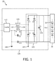
- FIG. 1 illustrates an example of an apparatus 10 which includes an isolating power supply 100 supplying power to a light emitting diode (LED) load 20.
- LED light emitting diode
- isolated power supply is understood to mean a power supply which is configured to receive electrical power at an input side thereof and to supply electrical power (e.g., to an LED load) at an output side thereof, and which provides galvanic isolation between the input side and the output side in the absence of parasitic effects, for example for safety reasons.
- apparatus 10 may comprise a lighting unit, including for example a lighting fixture.
- Isolating power supply 100 includes an inverter 110, an isolation transformer 120, a rectifier 130, and a filter or smoothing capacitor (Co) 135.
- inverter 110 may be replaced by another AC electrical power source, or may be eliminated - in which case isolating power supply 100 receives AC electrical power from an external source or supply.
- Isolation transformer 120 includes at least a first or primary winding 122 at a primary or input side thereof and a second or secondary winding 124 at a secondary or output side thereof.
- isolation transformer 120 may include additional auxiliary windings for example for sensing one or more current or voltages of isolating power supply 100.
- Rectifier 130 is a full wave rectifier configured as a diode bridge. Rectifier 130 has a pair of input terminals and a pair of output terminals, wherein the input terminals of the rectifier are connected to the output terminals of isolation transformer 120 and the output terminals of the rectifier are connected across LED load 20.
- the rectifier comprises: a first diode D1 connected from a first one of the input terminals of rectifier 130 to a first one of the output terminals of rectifier 130, a second diode D2 connected from a second one of the input terminals of rectifier 130 to the first one of the output terminals of rectifier 130, a third diode D3 connected from a second one of the output terminals of rectifier 130 to the first one of the input terminals of rectifier 130, and a fourth diode D4 connected from the second one of the output terminals of rectifier 130 to the second one of the input terminals of rectifier 130.
- LED load 20 includes a plurality of LEDs 22 connected in one or more strings.
- LEDs 22 may include any desired combination of white and/or colored LEDs to produce a desired colored light of a desired intensity.
- the color temperature may be selected to have a desired value by appropriate choices of the various LEDs which are employed.
- LED load 20 may be replaced by a different load, including for example other lighting devices besides LEDs.
- apparatus 10 may include a controller having one or more processors for controlling the electrical power which is supplied to LED load 20 to produce a desired lighting effect.
- apparatus 10 may also include one or more current and/or voltage sensors for sensing appropriate voltage(s) and/or current(s) in apparatus 10 to provide feedback for such a controller.
- a processor may be provided external to apparatus 10.
- inverter 110 receives at its input DC electrical power and outputs high frequency AC electrical power to the input of isolation transformer 120.
- the DC electrical power received by inverter 110 has a voltage of about 460V and AC electrical power output by inverter has a voltage regulated at a certain level according to output requirements.
- the frequency of the high frequency AC electrical power is at least 10 kHz. In some embodiments, the frequency of the high frequency AC electrical power is between approximately 40 kHz and approximately 100 kHz.
- Isolation transformer 120 provides galvanic isolation between the input side thereof at primary winding 122 and the secondary side thereof at secondary winding 124. More specifically, isolation transformer 120 provides galvanic isolation between the output of inverter 110 and the rectifier 130 and LED load 20.
- apparatus 100 may further include one or more safety capacitors between primary ground 102 and earth ground, and one or more additional safety capacitors between secondary ground 104 and earth ground.
- primary ground 102 may be directly tied to secondary ground 104 with one or more safety capacitors. These safety capacitors provide electromagnetic noise reduction for apparatus 10. The capacitance formed by these safety capacitors is represented by Cp-s between primary ground 102 and secondary ground 104, as shown in FIG. 1 .
- a stray capacitance exists between the primary and secondary windings 122 and 124 of isolation transformer 120.
- This stray capacitance is distributed in a way depending on the construction of isolation transformer 120 (e.g., how isolation transformer 120 is wound).
- This distributed stray capacitance can be represented as a single capacitance Cp as shown in FIG. 1 .
- This stray capacitance Cp can be connected between any two pins of isolation transformer 120 across the primary and secondary windings 122 and 124 depending on the way isolation transformer 120 is constructed (e.g., how isolation transformer 120 is wound), for example, 1S to 2S, 1F to 2F, etc. It should be understood that the connection of Cp from 1F to 2S which is illustrated in FIG. 1 is only one representative connection.
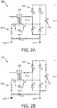
- Parasitic capacitances Cp and CP-s together with other circuit components form a charge pump and boost the output voltage Vout across smoothing capacitor 135 and the output of rectifier 130 when the isolating power supply 100 is open loaded (LED load 20 missing or open circuited, e.g., due to a component failure) or lightly loaded, as will be explained below with respect to FIGS. 2A, 2B and 3 , where it is assumed that the output of rectifier 130 is lightly loaded.
- FIG. 2A illustrates a circuit 200 which is a portion of an example of isolating power supply 100 with annotations or arrows 205 illustrating a current path during a charging interval of a charge pump created by the parasitic capacitances Cp and Cp-s.
- Reference numbers and characters in FIG. 2A that are the same as in FIG. 1 designate the same elements and features, a description of which will not be repeated.
- the charging interval represents one half of a period of the AC electrical power which is supplied to circuit 200 (e.g., by inverter 110).
- FIG. 2B illustrates the behavior of circuit 200 of isolating power supply 100 with annotations or arrows 205 illustrating a current path during a discharging interval of a charge pump effect created by parasitic capacitances Cp and Cp-s.
- Reference numbers and characters in FIG. 2B that are the same as in FIG. 1 designate the same elements and features, a description of which will not be repeated.
- the discharging interval represents one half of a period of the AC electrical power which is supplied to circuit 200 (e.g., by inverter 110).
- Cp is fully discharged only when the load is greater than a required minimum load for eliminating the charge pump effect, as given in equation 1 below.
- the voltage across Cp is positive and in the same direction as the voltage across secondary transformer winding 124.
- the peak voltage across secondary transformer winding 124 is still V2_pk due to the symmetry of the transformer voltage in a switching cycle. Therefore the total voltage seen by smoothing capacitor 135 is (V2_pk + Vcp), and the peak is larger than V2_pk. This results in an output voltage Vout which is greater than V2_pk. As explained above, this is undesirable.
- I min _ Ioad V 2 _ pk ⁇ Cp ⁇ Fsw , where Fsw is the switching frequency of the circuit;
- the output voltage Vout will be higher than V2_pk.
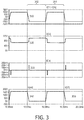
- FIG. 3 illustrates simulated examples of voltage and current waveforms for circuit 120 during a charging interval 302 and a discharging interval 304 of the charge pump effect created by parasitic capacitances Cp and Cp-s, as illustrated in FIGS. 2A and 2B .
- the input AC voltage provided to primary winding 122 is 100V in magnitude and 50 kHz in frequency.
- isolation transformer 120 has a 1:1 turns ratio between primary winding 122 and secondary winding 124.
- FIG. 3 shows five waveforms 310, 320, 330, 340 and 350, stacked vertically and synchronized in time.
- the horizontal axis (x-axis) represents time and the vertical axis (y-axis) represents voltage or current, depending on the waveform.
- x-axis represents time
- y-axis represents voltage or current, depending on the waveform.
- the first waveform 310 shows V2_pk, which is a reflected voltage of primary winding 122.
- V2_pk is a reflected voltage of primary winding 122.
- the second waveform 320 shows Vcp, the voltage across parasitic capacitance Cp. Note the lower voltage of the voltage pulses during a discharge interval 304 is not zero but about 65V. This is because parasitic capacitance Cp is not completely discharged during discharging interval 304. Parasitic capacitance Cp can only be discharged to LED load 20 during discharging interval 304. When LED load 20 is missing, open, or too light (not a low enough impedance to dump all the charge which built up in parasitic capacitance Cp in charging interval 302), a DC voltage remains across parasitic capacitance Cp at the end of discharging interval 304. This DC voltage added to the V2_pk to make the output voltage Vout greater than V2_pk during the discharging cycle.
- the third waveform 330 shows the charging and discharging current through parasitic capacitance Cp. Positive pulses represent the charging current, and negative pulses represent the discharging current. At steady state, the charging current is equal to the discharging current. Note: the DC voltage across parasitic capacitance Cp is charged up during the transient time when circuit 200 has not reached steady state yet.
- the fourth waveform 340 shows the voltage across D3, which is the sum of the V2_pk (100V) and Vcp during discharging interval 304. Due to the non-zero Vcp (about 65V), this voltage is about 165V during discharging interval 304, and as a result Vout (shown in fifth waveform 350) remains at about 165V during the entire switching period of the AC electrical power, much higher than V2_pk (100V).
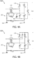
- FIG. 4A illustrates an example embodiment of a circuit 400A of an isolating power supply which includes a compensation element for compensating for an increase in an output voltage due to a charge pump effect created by parasitic capacitances.
- Reference numbers and characters in FIG. 4A that are the same as in FIG. 1 designate the same elements and features, a description of which will not be repeated.
- Circuit 400A includes a compensation capacitor 410 which is connected across diode D3 (in parallel with diode D3) of rectifier 130.
- FIG. 4A illustrates the behavior of a circuit 400A with annotations or arrows 205 illustrating a current path during a discharging interval of a charge pump effect created by parasitic capacitances Cp and Cp-s.
- the charge which has built up in parasitic capacitance Cp during the charging interval is dumped to compensation capacitor 410 and as a result no charge is transferred to smoothing capacitor 135. Accordingly, the voltage across smoothing capacitor 135 is equal to the peak voltage of winding 2 (V2_pk).
- the capacitance of compensation capacitor 410 is about the same as the parasitic capacitance Cp. In some embodiments, the capacitance of compensation capacitor 410 is approximately the same as the parasitic capacitance Cp. In some embodiments, the capacitance of compensation capacitor 410 equals the parasitic capacitance Cp, within a component tolerance value of compensation capacitor 410.
- compensation capacitor 410 can be connected across diode D1 (in parallel with diode D1).
- FIG. 4B illustrates such an alternative circuit 400B where capacitor 410 is connected across diode D1.
- the same reference numbers and characters are employed as in FIG. 4A .
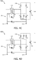
- FIGS. 4C and 4D illustrate alternative circuits 400C and 400D, where capacitor 410 is connected across diode D4 in FIG. 4C and connected across diode D2 in FIG. 4D .
- FIGS. 4C and 4D the same reference numbers and characters are employed as in FIG. 4A .
- the compensation means is a compensation capacitor which is connected across one of the diodes of rectifier 130: (1) the capacitance of the compensation capacitor should be reasonably close to the parasitic capacitance Cp; and (2) the compensation capacitor needs to be provided on a particular "leg" of rectifier 130 depending on the construction/configuration of isolation transformer 120.
- the parasitic capacitance Cp may be unknown and/or may vary significantly from isolation transformer 120 to isolation transformer 120, or from circuit to circuit. Accordingly, it may be difficult in some cases to insure that the capacitance of the compensation capacitor is reasonably close to the parasitic capacitance Cp.
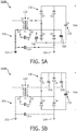
- FIGS. 5A and 5B illustrate additional embodiments which use a compensation capacitor on each leg of rectifier 130.
- FIG. 5A illustrates a circuit 500A of an isolating power supply which includes compensation elements for compensating for an increase in an output voltage due to a charge pump effect created by parasitic capacitances.
- Reference numbers and characters in FIG. 5 that are the same as in FIG. 1 designate the same elements and features, a description of which will not be repeated.
- Circuit 500A includes as compensation means a first compensation capacitor 510 which is connected across diode D3 (in parallel with diode D3) of rectifier 130 and a second compensation capacitor 520 which is connected across diode D4 (in parallel with diode D4) of rectifier 130.
- first and second compensation capacitors 510 and 520 should be close to each other and much greater than parasitic capacitance Cp.
- the charge in parasitic capacitance Cp is absorbed by the larger capacitance C3 or C4, depending on the way the stray capacitance Cp is connected across the various terminals of isolation transformer 120, according to the configuration/construction of isolation transformer 120 (e.g., how isolation transformer 120 is wound).
- the output voltage Vout is close to the peak voltage V2_pk of secondary winding 124.
- the capacitance of first compensation capacitor 510 is about the same as the capacitance of second compensation capacitor 520. In some embodiments, the capacitance of first compensation capacitor 510 is approximately the same as the capacitance of second compensation capacitor 520. In some embodiments, the capacitance of first compensation capacitor 510 equals the capacitance of second compensation capacitor 520, within a component tolerance value of first and second compensation capacitors 510 and 520.
- the capacitance of first compensation capacitor 510 and the capacitance of second compensation capacitor 520 are each at least twice the parasitic capacitance Cp. In some embodiments, the capacitance of first compensation capacitor 510 and the capacitance of second compensation capacitor 520 are each at least approximately ten times the parasitic capacitance Cp.
- first compensation capacitor 510 can be connected across diode D1 (in parallel with diode D1) and second compensation capacitor 520 can be connected across diode D2 (in parallel with diode D2).
- circuit 500A which includes as compensation means first and second compensation capacitors 510 and 520 has an advantage that it will compensate for a charge pump effect caused by parasitic capacitance regardless of how isolation transformer 120 is configured or constructed. Furthermore, it is not necessary to know and precisely match the value of parasitic capacitance Cp - all that is needed is that the capacitance values of first and second compensation capacitors 510 and 520 should be close (preferably equal) to each other and much greater than parasitic capacitance Cp.
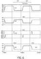
- FIG. 6 illustrates simulated examples of voltage and current waveforms for the example embodiments of an isolating power supply with compensation means for compensating for an increase in an output voltage due to a charge pump effect created by parasitic capacitances which are illustrated in FIGS. 4 and 5 .
- FIG. 6 shows five waveforms 310, 620, 630, 640 and 650, stacked vertically and synchronized in time.
- the horizontal axis (x-axis) represents time and the vertical axis (y-axis) represents voltage or current, depending on the waveform.
- x-axis represents time
- y-axis represents voltage or current, depending on the waveform.
- the first waveform 310 shows V2_pk (the same as in FIG. 3 )
- the second waveform 620 shows Vcp
- the third waveform 630 shows the charging and discharging current through parasitic capacitance Cp
- the fourth waveform 640 shows the voltage across diode D3
- the fifth waveform 650 shows the output voltage Vout.
- the bottom level of the voltage VCP during discharge interval 304 is zero. This is because all the charge in parasitic capacitance Cp is dumped to first compensation capacitor 510 during discharging interval 304.
- the voltage across diode D3 is now equal to V2_pk during discharging interval 304 because the voltage across parasitic capacitance Cp is completely discharged to zero.
- the fifth waveform 650, Vout follows V2_pk at 100V. Accordingly, an increase in the output voltage caused by a charge pump effect of the parasitic capacitor Cp is compensated, and the output voltage is not increased.
- the required minimum load current for eliminating the charge pump effect is directly proportional to output voltage Vout, the switching frequency, and the stray capacitance Cp of the isolation transformer.
- the output voltage Vout typically is determined by design requirements and cannot be changed, but the other two factors can be used to a certain extent to improve this charge pump effect.
- the isolation transformer can be constructed to minimize the stray capacitance Cp.
- the switching frequency can be set as low as possible. However, limit for these two design optimizations does exist due to other design constrains such as transformer size and power losses requirements.
- isolation transformer 120 is connected in a circuit. To minimize the charge pump effect, primary and secondary windings 122 and 124 of isolation transformer 120 should be connected in such a way that the total voltage produced by these two windings in the charging path is at the minimum. From this standpoint, the worst connection of isolation transformer 120 occurs where the voltages from both primary and secondary windings reinforce each other.
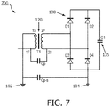
- FIG. 7 illustrates a circuit 700 of an isolating power supply.
- Reference numbers and characters in FIG. 7 that are the same as in FIG. 1 designate the same elements and features, a description of which will not be repeated.
- a difference between circuit 700 and circuit 200 is the way that isolation transformer 120 is connected on the primary side in circuit 700.
- the voltages from both primary and secondary windings 122 and 124 of isolation transformer 120 reinforce each other.
- the charge pump effect generated by circuit 700 is worse than that of circuit 200.
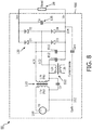
- FIG. 8 illustrates an example of an apparatus 80 which includes an isolating power supply having a circuit 800 with compensation means for compensating for an increase in an output voltage due to a charge pump effect created by parasitic capacitances.
- Reference numbers and characters in FIG. 8 that are the same as in FIG. 1 designate the same elements and features, a description of which will not be repeated.
- circuit 800 of apparatus 800 is similar to circuit 500A, with the following significant differences.
- circuit 800 includes an AC voltage source 118 in lieu of inverter 100. It should be understood that either inverter 110 or AC voltage source 118 could be employed with the circuits of FIGS. 4A-D and 5A-B .
- circuit 800 includes as compensation elements one or both of compensation capacitors 810 and/or 812, as discussed above with respect to FIGS. 4A-D and 5A-B .
- circuit 800 includes a (small) current sense transformer 820 in the secondary AC current path.
- the sensed current should however not include the current generated by first/second compensation capacitor(s) 810 or 812, since this will give a distorted measurement which becomes clearly visible when going to low output currents.
- current sense transformer 820 By placing current sense transformer 820 in the right location one can still have the compensation for parasitic capacitance Cp by the added compensation capacitor(s) 810 and/or 812, and maintain an accurate current measurement.
- current sense transformer 820 has a primary winding connected between one of the output terminals of isolation transformer 120 and one of the input terminals of rectifier 130, and second capacitor 812 is connected between the one of the output terminals of isolation transformer 120 and one of the output terminals of rectifier 130.
Landscapes
- Engineering & Computer Science (AREA)
- Power Engineering (AREA)
- Physics & Mathematics (AREA)
- Electromagnetism (AREA)
- Circuit Arrangement For Electric Light Sources In General (AREA)
- Dc-Dc Converters (AREA)
- Rectifiers (AREA)
Claims (18)
- Appareil (500A, 500B, 800) pour fournir de l'énergie à une charge de diode électroluminescente, DEL (20), l'appareil comprenant :un transformateur d'isolation (120) ayant une paire de bornes d'entrée (1S/1F) configurées pour recevoir de l'énergie électrique en CA et ayant une paire de bornes de sortie (2S/2F), dans lequel le transformateur d'isolation fournit une isolation CC entre les bornes d'entrée sur un côté primaire de celui-ci et les bornes de sortie sur un côté secondaire de celui-ci ;un redresseur (130) ayant une paire de bornes d'entrée et une paire de bornes de sortie, dans lequel les bornes d'entrée du redresseur sont raccordées aux bornes de sortie du transformateur d'isolation et les bornes de sortie du redresseur sont raccordées à travers la charge de DEL et dans lequel le redresseur comprend :une première diode (D1) raccordée à partir d'une première borne d'entrée des bornes d'entrée du redresseur à une première borne de sortie des bornes de sortie du redresseur,une deuxième diode (D2) raccordée à partir d'une seconde borne d'entrée des bornes d'entrée du redresseur à une première borne de sortie des bornes de sortie du redresseur,une troisième diode (D3) raccordée à partir d'une seconde borne de sortie des bornes de sortie du redresseur à une première borne d'entrée des bornes d'entrée du redresseur,une quatrième diode (D4) raccordée à partir d'une seconde borne de sortie des bornes de sortie du redresseur à une seconde borne d'entrée des bornes d'entrée du redresseur ; etdes premier et second condensateurs (510/520, 810/812), dans lequel une première capacité du premier condensateur est approximativement la même qu'une seconde capacité du second condensateur etdans lequel soit :le premier condensateur (510, 810) est raccordé au moyen de la première diode (D1) et le second condensateur (520, 812) est raccordé au moyen de la deuxième diode (D2), soitle premier condensateur (510, 810) est raccordé au moyen de la troisième diode (D3) et le second condensateur (520, 812) est raccordé au moyen de la quatrième diode (D4).
- Appareil (500A, 500B, 800) selon la revendication 1, dans lequel le transformateur d'isolation présente une capacité parasite entre l'une des bornes d'entrée et l'une des bornes de sortie et
dans lequel la première capacité et la seconde capacité font chacune au moins deux fois la capacité parasite. - Appareil (500A, 500B, 800) selon la revendication 1, dans lequel le transformateur d'isolation présente une capacité parasite entre l'une des bornes d'entrée et l'une des bornes de sortie et dans lequel la première capacité et la seconde capacité font chacune au moins approximativement dix fois la capacité parasite.
- Appareil (800) selon la revendication 1, comprenant en outre un transformateur de détection de courant (820) configuré pour détecter un courant sur le côté secondaire du transformateur d'isolation, dans lequel le transformateur de détection de courant présente un enroulement primaire raccordé entre l'une des bornes de sortie du transformateur d'isolation et l'une des bornes d'entrée du redresseur.
- Appareil (500A, 500B, 800) selon la revendication 1, comprenant en outre une alimentation CA (110, 118) raccordée aux bornes d'entrée du transformateur d'isolation et configurée pour fournir l'énergie électrique en CA au transformateur d'isolation.
- Appareil (500A, 500B, 800) selon la revendication 5, dans lequel l'alimentation CA (110, 118) est configurée pour fournir l'énergie électrique en CA à une fréquence d'au moins 10 kHz.
- Appareil (500A, 500B, 800) selon la revendication 5, dans lequel l'alimentation CA (110, 118) est configurée pour fournir l'énergie électrique en CA à une fréquence d'entre approximativement 40 kHz et approximativement 100 kHz
- Appareil (500A, 500B, 800) selon la revendication 5, dans lequel l'alimentation CA comprend un convertisseur continu-alternatif (110).
- Appareil (500A, 500B, 800) selon la revendication 1, comprenant en outre la charge de DEL (20), dans lequel la charge de DEL comprend au moins un chapelet de DEL.
- Appareil (400A, 400B, 400C, 400D) pour fournir de l'énergie à une charge de diode électroluminescente, DEL (20), l'appareil comprenant :un transformateur d'isolation (120) ayant une paire de bornes d'entrée (1S/1F) configurées pour recevoir de l'énergie électrique en CA et ayant une paire de bornes de sortie (2S/2F), dans lequel le transformateur d'isolation présente une capacité parasite (Cp) entre l'une des bornes d'entrée et l'une des bornes de sortie et dans lequel le transformateur d'isolation fournit une isolation CC entre les bornes d'entrée sur un côté primaire de celui-ci et les bornes de sortie sur un côté secondaire de celui-ci ;un redresseur (130) ayant une paire de bornes d'entrée et une paire de bornes de sortie, dans lequel les bornes d'entrée du redresseur sont raccordées aux bornes de sortie du transformateur d'isolation et les bornes de sortie du redresseur sont raccordées à travers la charge de DEL et dans lequel le redresseur comprend une pluralité de diodes (D1/D2/D3/D4) raccordées dans un pont de diode ; etun condensateur de compensation (410) raccordé à travers l'une des diodes du pont de diode,dans lequel une capacité du condensateur de compensation est environ la même que la capacité parasite.
- Appareil (400A, 400B, 400C, 400D) selon la revendication 10, comprenant en outre une alimentation CA (110, 118) raccordée aux bornes d'entrée du transformateur d'isolation et configurée pour fournir l'énergie électrique en CA au transformateur d'isolation.
- Appareil (400A, 400B, 400C, 400D) selon la revendication 11, dans lequel l'alimentation CA (110, 118) est configurée pour fournir l'énergie électrique en CA à une fréquence d'au moins 10 kHz.
- Appareil (400A, 400B, 400C, 400D) selon la revendication 11, dans lequel l'alimentation CA (110, 118) est configurée pour fournir l'énergie électrique en CA à une fréquence d'entre approximativement 40 kHz et approximativement 100 kHz
- Appareil (400A, 400B, 400C, 400D) selon la revendication 10, dans lequel le pont de diode comprend :une première diode (D1) raccordée à partir d'une première borne d'entrée des bornes d'entrée du redresseur à une première borne de sortie des bornes de sortie du redresseur,une deuxième diode (D2) raccordée à partir d'une seconde borne d'entrée des bornes d'entrée du redresseur à une première borne de sortie des bornes de sortie du redresseur,une troisième diode (D3) raccordée à partir d'une seconde borne de sortie des bornes de sortie du redresseur à une première borne d'entrée des bornes d'entrée du redresseur,une quatrième diode (D4) raccordée à partir d'une seconde borne de sortie des bornes de sortie du redresseur à une seconde borne d'entrée des bornes d'entrée du redresseur,dans lequel le condensateur de compensation est raccordé à travers l'une des première, deuxième, troisième et quatrième diodes.
- Appareil (400A, 400B, 400C, 400D) selon la revendication 11, dans lequel l'alimentation CA comprend un convertisseur continu-alternatif (110).
- Appareil (400A, 400B, 400C, 400D) selon la revendication 10, comprenant en outre la charge de DEL (20), dans lequel la charge de DEL comprend au moins un chapelet de DEL.
- Appareil (400A, 400B, 400C, 400D, 500A, 500B, 800) pour fournir de l'énergie à une charge de diode électroluminescente, DEL (20), l'appareil comprenant :un transformateur d'isolation (110) ayant une paire de bornes d'entrée (1S/1F) configurées pour recevoir de l'énergie électrique en CA et ayant une paire de bornes de sortie (2S/2F), dans lequel le transformateur d'isolation présente une capacité parasite (Cp) entre l'une des bornes d'entrée et l'une des bornes de sortie et dans lequel le transformateur d'isolation fournit une isolation CC entre les bornes d'entrée sur un côté primaire de celui-ci et les bornes de sortie sur un côté secondaire de celui-ci ;un redresseur (120) ayant une paire de bornes d'entrée et une paire de bornes de sortie, dans lequel les bornes d'entrée du redresseur sont raccordées aux bornes de sortie du transformateur d'isolation et les bornes de sortie du redresseur sont raccordées à travers la sortie de l'appareil et dans lequel le redresseur comprend une pluralité de diodes (D1/D2/D3/D4) raccordées dans un pont de diode ; etun moyen de compensation (410, 510/520, 810/812) pour compenser une augmentation d'une tension de sortie à travers la sortie de l'appareil en raison d'un effet de pompe de charge de la capacité parasite, le moyen de compensation comprenant au moins un condensateur de compensation raccordé à travers l'une des diodes du pont de diode.
- Appareil (500A, 500B, 800) selon la revendication 17, dans lequel le moyen de compensation comprend deux condensateurs de compensation (510/520, 810/812) raccordés chacun à travers une diode correspondante des diodes du pont de diode.
Applications Claiming Priority (2)
| Application Number | Priority Date | Filing Date | Title |
|---|---|---|---|
| US201462049074P | 2014-09-11 | 2014-09-11 | |
| PCT/IB2015/056803 WO2016038523A1 (fr) | 2014-09-11 | 2015-09-06 | Compensation de l'effet de pompe de charge pour transformateur de séparation à haute fréquence dans des alimentations électriques de dispositif d'éclairage. |
Publications (2)
| Publication Number | Publication Date |
|---|---|
| EP3192157A1 EP3192157A1 (fr) | 2017-07-19 |
| EP3192157B1 true EP3192157B1 (fr) | 2021-05-05 |
Family
ID=54251551
Family Applications (1)
| Application Number | Title | Priority Date | Filing Date |
|---|---|---|---|
| EP15774982.1A Active EP3192157B1 (fr) | 2014-09-11 | 2015-09-06 | Compensation de l'effet de pompe de charge pour transformateur de séparation à haute fréquence dans des alimentations électriques de dispositif d'éclairage. |
Country Status (5)
| Country | Link |
|---|---|
| US (1) | US10110118B2 (fr) |
| EP (1) | EP3192157B1 (fr) |
| CN (1) | CN106688170B (fr) |
| ES (1) | ES2881343T3 (fr) |
| WO (1) | WO2016038523A1 (fr) |
Families Citing this family (2)
| Publication number | Priority date | Publication date | Assignee | Title |
|---|---|---|---|---|
| CN110445386A (zh) * | 2019-06-20 | 2019-11-12 | 广东博德新能源技术有限公司 | 一种两级隔离电源 |
| CN111628641B (zh) * | 2020-05-25 | 2022-01-11 | 中国长城科技集团股份有限公司 | 无桥整流电路、漏电流峰值控制方法及可读存储介质 |
Family Cites Families (11)
| Publication number | Priority date | Publication date | Assignee | Title |
|---|---|---|---|---|
| US3562623A (en) | 1968-07-16 | 1971-02-09 | Hughes Aircraft Co | Circuit for reducing stray capacity effects in transformer windings |
| US4541041A (en) | 1983-08-22 | 1985-09-10 | General Electric Company | Full load to no-load control for a voltage fed resonant inverter |
| FR2627644B1 (fr) | 1988-02-24 | 1991-05-03 | Europ Agence Spatiale | Convertisseur continu-continu, sans pertes de commutation, notamment pour alimentation continue haute frequence ou pour amplificateur a tube a ondes progressives |
| FR2658674B1 (fr) | 1990-02-20 | 1992-05-07 | Europ Agence Spatiale | Convertisseur continu-continu a commutation a tension nulle. |
| US5539630A (en) | 1993-11-15 | 1996-07-23 | California Institute Of Technology | Soft-switching converter DC-to-DC isolated with voltage bidirectional switches on the secondary side of an isolation transformer |
| KR19990076761A (ko) * | 1995-12-29 | 1999-10-15 | 맨프래드 메이어 | 에너지 손실이 최소화된 능동 정류기 |
| JP3975653B2 (ja) * | 2000-06-12 | 2007-09-12 | 松下電工株式会社 | 放電灯点灯装置 |
| DE102004050060B4 (de) * | 2004-10-13 | 2018-02-08 | Osram Gmbh | Tiefsetzerschaltung |
| KR101008458B1 (ko) * | 2009-03-23 | 2011-01-14 | 삼성전기주식회사 | Led 구동 회로 |
| JP5440266B2 (ja) * | 2010-03-05 | 2014-03-12 | 富士電機株式会社 | 電力変換装置 |
| EP2421138A1 (fr) * | 2010-08-18 | 2012-02-22 | ABB Oy | Photovoltaïque convertisseur continu/continu isolé |
-
2015
- 2015-09-06 EP EP15774982.1A patent/EP3192157B1/fr active Active
- 2015-09-06 ES ES15774982T patent/ES2881343T3/es active Active
- 2015-09-06 US US15/509,404 patent/US10110118B2/en active Active
- 2015-09-06 WO PCT/IB2015/056803 patent/WO2016038523A1/fr not_active Ceased
- 2015-09-06 CN CN201580048696.8A patent/CN106688170B/zh active Active
Also Published As
| Publication number | Publication date |
|---|---|
| US20170279347A1 (en) | 2017-09-28 |
| US10110118B2 (en) | 2018-10-23 |
| WO2016038523A1 (fr) | 2016-03-17 |
| ES2881343T3 (es) | 2021-11-29 |
| CN106688170B (zh) | 2020-03-13 |
| CN106688170A (zh) | 2017-05-17 |
| EP3192157A1 (fr) | 2017-07-19 |
Similar Documents
| Publication | Publication Date | Title |
|---|---|---|
| US9163815B2 (en) | Power converter device for driving solid state lighting load | |
| EP2656691B1 (fr) | Procédé et appareil pour limiter un dépassement et un sous-dépassement de courant dans un pilote de lumière | |
| US8624513B2 (en) | Multichannel lighting unit and driver for supplying current to light sources in multichannel lighting unit | |
| US9433055B2 (en) | Lighting device and illumination apparatus including same | |
| US10548189B2 (en) | Control of isolated auxiliary power supply and DALI supply for sensor-ready LED drivers | |
| US9265132B2 (en) | Linear driver for reduced perceived light flicker | |
| JP2012134153A (ja) | 蛍光照明システムのための発光ダイオード組込み装置 | |
| EP2850916B1 (fr) | Circuit pilote pour des sources de lumière à l'état solide | |
| EP2609789B1 (fr) | Procédés et appareil de commande de diodes électroluminescentes (del) comprenant des étages de conversion flyback en parallèle | |
| WO2009095890A2 (fr) | Bloc d'alimentation à mode commuté | |
| WO2018041687A1 (fr) | Contrôle d'alimentation électrique auxiliaire isolée et alimentation dali pour circuits de commande de del utilisables avec des capteurs | |
| US10110118B2 (en) | Charge pump effect compensation for high frequency isolation transformer in lighting device power supplies | |
| WO2025096866A1 (fr) | Générateur de lumière blanche ayant une conception modulaire et interchangeable | |
| US11856666B2 (en) | Alternating current source direct driving LED lighting device | |
| FI20245091A1 (en) | Current balancing apparatus, led driving circuit and lightning arrangement |
Legal Events
| Date | Code | Title | Description |
|---|---|---|---|
| STAA | Information on the status of an ep patent application or granted ep patent |
Free format text: STATUS: THE INTERNATIONAL PUBLICATION HAS BEEN MADE |
|
| PUAI | Public reference made under article 153(3) epc to a published international application that has entered the european phase |
Free format text: ORIGINAL CODE: 0009012 |
|
| STAA | Information on the status of an ep patent application or granted ep patent |
Free format text: STATUS: REQUEST FOR EXAMINATION WAS MADE |
|
| 17P | Request for examination filed |
Effective date: 20170411 |
|
| AK | Designated contracting states |
Kind code of ref document: A1 Designated state(s): AL AT BE BG CH CY CZ DE DK EE ES FI FR GB GR HR HU IE IS IT LI LT LU LV MC MK MT NL NO PL PT RO RS SE SI SK SM TR |
|
| AX | Request for extension of the european patent |
Extension state: BA ME |
|
| RIN1 | Information on inventor provided before grant (corrected) |
Inventor name: SONG, ZHIHUA Inventor name: VAN DIJK, BERNHARD CHRISTIAAN Inventor name: ZHENG, SANBAO |
|
| DAV | Request for validation of the european patent (deleted) | ||
| DAX | Request for extension of the european patent (deleted) | ||
| RAP1 | Party data changed (applicant data changed or rights of an application transferred) |
Owner name: PHILIPS LIGHTING HOLDING B.V. |
|
| RAP1 | Party data changed (applicant data changed or rights of an application transferred) |
Owner name: SIGNIFY HOLDING B.V. |
|
| STAA | Information on the status of an ep patent application or granted ep patent |
Free format text: STATUS: EXAMINATION IS IN PROGRESS |
|
| 17Q | First examination report despatched |
Effective date: 20200226 |
|
| GRAP | Despatch of communication of intention to grant a patent |
Free format text: ORIGINAL CODE: EPIDOSNIGR1 |
|
| STAA | Information on the status of an ep patent application or granted ep patent |
Free format text: STATUS: GRANT OF PATENT IS INTENDED |
|
| INTG | Intention to grant announced |
Effective date: 20201204 |
|
| GRAS | Grant fee paid |
Free format text: ORIGINAL CODE: EPIDOSNIGR3 |
|
| GRAA | (expected) grant |
Free format text: ORIGINAL CODE: 0009210 |
|
| STAA | Information on the status of an ep patent application or granted ep patent |
Free format text: STATUS: THE PATENT HAS BEEN GRANTED |
|
| AK | Designated contracting states |
Kind code of ref document: B1 Designated state(s): AL AT BE BG CH CY CZ DE DK EE ES FI FR GB GR HR HU IE IS IT LI LT LU LV MC MK MT NL NO PL PT RO RS SE SI SK SM TR |
|
| REG | Reference to a national code |
Ref country code: GB Ref legal event code: FG4D |
|
| REG | Reference to a national code |
Ref country code: CH Ref legal event code: EP |
|
| REG | Reference to a national code |
Ref country code: AT Ref legal event code: REF Ref document number: 1391079 Country of ref document: AT Kind code of ref document: T Effective date: 20210515 |
|
| REG | Reference to a national code |
Ref country code: DE Ref legal event code: R096 Ref document number: 602015069007 Country of ref document: DE |
|
| REG | Reference to a national code |
Ref country code: IE Ref legal event code: FG4D |
|
| REG | Reference to a national code |
Ref country code: SE Ref legal event code: TRGR |
|
| REG | Reference to a national code |
Ref country code: LT Ref legal event code: MG9D |
|
| REG | Reference to a national code |
Ref country code: AT Ref legal event code: MK05 Ref document number: 1391079 Country of ref document: AT Kind code of ref document: T Effective date: 20210505 |
|
| PG25 | Lapsed in a contracting state [announced via postgrant information from national office to epo] |
Ref country code: AT Free format text: LAPSE BECAUSE OF FAILURE TO SUBMIT A TRANSLATION OF THE DESCRIPTION OR TO PAY THE FEE WITHIN THE PRESCRIBED TIME-LIMIT Effective date: 20210505 Ref country code: BG Free format text: LAPSE BECAUSE OF FAILURE TO SUBMIT A TRANSLATION OF THE DESCRIPTION OR TO PAY THE FEE WITHIN THE PRESCRIBED TIME-LIMIT Effective date: 20210805 Ref country code: HR Free format text: LAPSE BECAUSE OF FAILURE TO SUBMIT A TRANSLATION OF THE DESCRIPTION OR TO PAY THE FEE WITHIN THE PRESCRIBED TIME-LIMIT Effective date: 20210505 Ref country code: LT Free format text: LAPSE BECAUSE OF FAILURE TO SUBMIT A TRANSLATION OF THE DESCRIPTION OR TO PAY THE FEE WITHIN THE PRESCRIBED TIME-LIMIT Effective date: 20210505 Ref country code: FI Free format text: LAPSE BECAUSE OF FAILURE TO SUBMIT A TRANSLATION OF THE DESCRIPTION OR TO PAY THE FEE WITHIN THE PRESCRIBED TIME-LIMIT Effective date: 20210505 |
|
| REG | Reference to a national code |
Ref country code: ES Ref legal event code: FG2A Ref document number: 2881343 Country of ref document: ES Kind code of ref document: T3 Effective date: 20211129 |
|
| PG25 | Lapsed in a contracting state [announced via postgrant information from national office to epo] |
Ref country code: LV Free format text: LAPSE BECAUSE OF FAILURE TO SUBMIT A TRANSLATION OF THE DESCRIPTION OR TO PAY THE FEE WITHIN THE PRESCRIBED TIME-LIMIT Effective date: 20210505 Ref country code: IS Free format text: LAPSE BECAUSE OF FAILURE TO SUBMIT A TRANSLATION OF THE DESCRIPTION OR TO PAY THE FEE WITHIN THE PRESCRIBED TIME-LIMIT Effective date: 20210905 Ref country code: GR Free format text: LAPSE BECAUSE OF FAILURE TO SUBMIT A TRANSLATION OF THE DESCRIPTION OR TO PAY THE FEE WITHIN THE PRESCRIBED TIME-LIMIT Effective date: 20210806 Ref country code: PT Free format text: LAPSE BECAUSE OF FAILURE TO SUBMIT A TRANSLATION OF THE DESCRIPTION OR TO PAY THE FEE WITHIN THE PRESCRIBED TIME-LIMIT Effective date: 20210906 Ref country code: PL Free format text: LAPSE BECAUSE OF FAILURE TO SUBMIT A TRANSLATION OF THE DESCRIPTION OR TO PAY THE FEE WITHIN THE PRESCRIBED TIME-LIMIT Effective date: 20210505 Ref country code: NO Free format text: LAPSE BECAUSE OF FAILURE TO SUBMIT A TRANSLATION OF THE DESCRIPTION OR TO PAY THE FEE WITHIN THE PRESCRIBED TIME-LIMIT Effective date: 20210805 Ref country code: RS Free format text: LAPSE BECAUSE OF FAILURE TO SUBMIT A TRANSLATION OF THE DESCRIPTION OR TO PAY THE FEE WITHIN THE PRESCRIBED TIME-LIMIT Effective date: 20210505 |
|
| REG | Reference to a national code |
Ref country code: NL Ref legal event code: MP Effective date: 20210505 |
|
| PG25 | Lapsed in a contracting state [announced via postgrant information from national office to epo] |
Ref country code: NL Free format text: LAPSE BECAUSE OF FAILURE TO SUBMIT A TRANSLATION OF THE DESCRIPTION OR TO PAY THE FEE WITHIN THE PRESCRIBED TIME-LIMIT Effective date: 20210505 |
|
| PG25 | Lapsed in a contracting state [announced via postgrant information from national office to epo] |
Ref country code: RO Free format text: LAPSE BECAUSE OF FAILURE TO SUBMIT A TRANSLATION OF THE DESCRIPTION OR TO PAY THE FEE WITHIN THE PRESCRIBED TIME-LIMIT Effective date: 20210505 Ref country code: SK Free format text: LAPSE BECAUSE OF FAILURE TO SUBMIT A TRANSLATION OF THE DESCRIPTION OR TO PAY THE FEE WITHIN THE PRESCRIBED TIME-LIMIT Effective date: 20210505 Ref country code: SM Free format text: LAPSE BECAUSE OF FAILURE TO SUBMIT A TRANSLATION OF THE DESCRIPTION OR TO PAY THE FEE WITHIN THE PRESCRIBED TIME-LIMIT Effective date: 20210505 Ref country code: EE Free format text: LAPSE BECAUSE OF FAILURE TO SUBMIT A TRANSLATION OF THE DESCRIPTION OR TO PAY THE FEE WITHIN THE PRESCRIBED TIME-LIMIT Effective date: 20210505 Ref country code: DK Free format text: LAPSE BECAUSE OF FAILURE TO SUBMIT A TRANSLATION OF THE DESCRIPTION OR TO PAY THE FEE WITHIN THE PRESCRIBED TIME-LIMIT Effective date: 20210505 Ref country code: CZ Free format text: LAPSE BECAUSE OF FAILURE TO SUBMIT A TRANSLATION OF THE DESCRIPTION OR TO PAY THE FEE WITHIN THE PRESCRIBED TIME-LIMIT Effective date: 20210505 |
|
| REG | Reference to a national code |
Ref country code: DE Ref legal event code: R097 Ref document number: 602015069007 Country of ref document: DE |
|
| PLBE | No opposition filed within time limit |
Free format text: ORIGINAL CODE: 0009261 |
|
| STAA | Information on the status of an ep patent application or granted ep patent |
Free format text: STATUS: NO OPPOSITION FILED WITHIN TIME LIMIT |
|
| 26N | No opposition filed |
Effective date: 20220208 |
|
| REG | Reference to a national code |
Ref country code: CH Ref legal event code: PL |
|
| REG | Reference to a national code |
Ref country code: BE Ref legal event code: MM Effective date: 20210930 |
|
| PG25 | Lapsed in a contracting state [announced via postgrant information from national office to epo] |
Ref country code: IS Free format text: LAPSE BECAUSE OF FAILURE TO SUBMIT A TRANSLATION OF THE DESCRIPTION OR TO PAY THE FEE WITHIN THE PRESCRIBED TIME-LIMIT Effective date: 20210905 Ref country code: MC Free format text: LAPSE BECAUSE OF FAILURE TO SUBMIT A TRANSLATION OF THE DESCRIPTION OR TO PAY THE FEE WITHIN THE PRESCRIBED TIME-LIMIT Effective date: 20210505 Ref country code: AL Free format text: LAPSE BECAUSE OF FAILURE TO SUBMIT A TRANSLATION OF THE DESCRIPTION OR TO PAY THE FEE WITHIN THE PRESCRIBED TIME-LIMIT Effective date: 20210505 |
|
| PG25 | Lapsed in a contracting state [announced via postgrant information from national office to epo] |
Ref country code: LU Free format text: LAPSE BECAUSE OF NON-PAYMENT OF DUE FEES Effective date: 20210906 Ref country code: IE Free format text: LAPSE BECAUSE OF NON-PAYMENT OF DUE FEES Effective date: 20210906 Ref country code: BE Free format text: LAPSE BECAUSE OF NON-PAYMENT OF DUE FEES Effective date: 20210930 |
|
| PG25 | Lapsed in a contracting state [announced via postgrant information from national office to epo] |
Ref country code: LI Free format text: LAPSE BECAUSE OF NON-PAYMENT OF DUE FEES Effective date: 20210930 Ref country code: CH Free format text: LAPSE BECAUSE OF NON-PAYMENT OF DUE FEES Effective date: 20210930 |
|
| PG25 | Lapsed in a contracting state [announced via postgrant information from national office to epo] |
Ref country code: HU Free format text: LAPSE BECAUSE OF FAILURE TO SUBMIT A TRANSLATION OF THE DESCRIPTION OR TO PAY THE FEE WITHIN THE PRESCRIBED TIME-LIMIT; INVALID AB INITIO Effective date: 20150906 |
|
| P01 | Opt-out of the competence of the unified patent court (upc) registered |
Effective date: 20230425 |
|
| PG25 | Lapsed in a contracting state [announced via postgrant information from national office to epo] |
Ref country code: CY Free format text: LAPSE BECAUSE OF FAILURE TO SUBMIT A TRANSLATION OF THE DESCRIPTION OR TO PAY THE FEE WITHIN THE PRESCRIBED TIME-LIMIT Effective date: 20210505 |
|
| PG25 | Lapsed in a contracting state [announced via postgrant information from national office to epo] |
Ref country code: MK Free format text: LAPSE BECAUSE OF FAILURE TO SUBMIT A TRANSLATION OF THE DESCRIPTION OR TO PAY THE FEE WITHIN THE PRESCRIBED TIME-LIMIT Effective date: 20210505 |
|
| PG25 | Lapsed in a contracting state [announced via postgrant information from national office to epo] |
Ref country code: TR Free format text: LAPSE BECAUSE OF FAILURE TO SUBMIT A TRANSLATION OF THE DESCRIPTION OR TO PAY THE FEE WITHIN THE PRESCRIBED TIME-LIMIT Effective date: 20210505 |
|
| PG25 | Lapsed in a contracting state [announced via postgrant information from national office to epo] |
Ref country code: MT Free format text: LAPSE BECAUSE OF FAILURE TO SUBMIT A TRANSLATION OF THE DESCRIPTION OR TO PAY THE FEE WITHIN THE PRESCRIBED TIME-LIMIT Effective date: 20210505 |
|
| PGFP | Annual fee paid to national office [announced via postgrant information from national office to epo] |
Ref country code: IT Payment date: 20250922 Year of fee payment: 11 |
|
| PGFP | Annual fee paid to national office [announced via postgrant information from national office to epo] |
Ref country code: GB Payment date: 20250923 Year of fee payment: 11 |
|
| PGFP | Annual fee paid to national office [announced via postgrant information from national office to epo] |
Ref country code: FR Payment date: 20250925 Year of fee payment: 11 |
|
| PGFP | Annual fee paid to national office [announced via postgrant information from national office to epo] |
Ref country code: SE Payment date: 20250924 Year of fee payment: 11 |
|
| PGFP | Annual fee paid to national office [announced via postgrant information from national office to epo] |
Ref country code: DE Payment date: 20251126 Year of fee payment: 11 |
|
| PGFP | Annual fee paid to national office [announced via postgrant information from national office to epo] |
Ref country code: ES Payment date: 20251015 Year of fee payment: 11 |