EP3192168B1 - Wien-brücke-oszillatorschaltung - Google Patents
Wien-brücke-oszillatorschaltung Download PDFInfo
- Publication number
- EP3192168B1 EP3192168B1 EP15839315.7A EP15839315A EP3192168B1 EP 3192168 B1 EP3192168 B1 EP 3192168B1 EP 15839315 A EP15839315 A EP 15839315A EP 3192168 B1 EP3192168 B1 EP 3192168B1
- Authority
- EP
- European Patent Office
- Prior art keywords
- circuit
- output
- wien bridge
- input
- coupled
- Prior art date
- Legal status (The legal status is an assumption and is not a legal conclusion. Google has not performed a legal analysis and makes no representation as to the accuracy of the status listed.)
- Active
Links
Images







Classifications
-
- H—ELECTRICITY
- H02—GENERATION; CONVERSION OR DISTRIBUTION OF ELECTRIC POWER
- H02M—APPARATUS FOR CONVERSION BETWEEN AC AND AC, BETWEEN AC AND DC, OR BETWEEN DC AND DC, AND FOR USE WITH MAINS OR SIMILAR POWER SUPPLY SYSTEMS; CONVERSION OF DC OR AC INPUT POWER INTO SURGE OUTPUT POWER; CONTROL OR REGULATION THEREOF
- H02M7/00—Conversion of AC power input into DC power output; Conversion of DC power input into AC power output
- H02M7/42—Conversion of DC power input into AC power output without possibility of reversal
- H02M7/44—Conversion of DC power input into AC power output without possibility of reversal by static converters
- H02M7/48—Conversion of DC power input into AC power output without possibility of reversal by static converters using discharge tubes with control electrode or semiconductor devices with control electrode
- H02M7/53—Conversion of DC power input into AC power output without possibility of reversal by static converters using discharge tubes with control electrode or semiconductor devices with control electrode using devices of a triode or transistor type requiring continuous application of a control signal
- H02M7/537—Conversion of DC power input into AC power output without possibility of reversal by static converters using discharge tubes with control electrode or semiconductor devices with control electrode using devices of a triode or transistor type requiring continuous application of a control signal using semiconductor devices only, e.g. single switched pulse inverters
- H02M7/5387—Conversion of DC power input into AC power output without possibility of reversal by static converters using discharge tubes with control electrode or semiconductor devices with control electrode using devices of a triode or transistor type requiring continuous application of a control signal using semiconductor devices only, e.g. single switched pulse inverters in a bridge configuration
- H02M7/53871—Conversion of DC power input into AC power output without possibility of reversal by static converters using discharge tubes with control electrode or semiconductor devices with control electrode using devices of a triode or transistor type requiring continuous application of a control signal using semiconductor devices only, e.g. single switched pulse inverters in a bridge configuration with automatic control of output voltage or current
-
- H—ELECTRICITY
- H02—GENERATION; CONVERSION OR DISTRIBUTION OF ELECTRIC POWER
- H02M—APPARATUS FOR CONVERSION BETWEEN AC AND AC, BETWEEN AC AND DC, OR BETWEEN DC AND DC, AND FOR USE WITH MAINS OR SIMILAR POWER SUPPLY SYSTEMS; CONVERSION OF DC OR AC INPUT POWER INTO SURGE OUTPUT POWER; CONTROL OR REGULATION THEREOF
- H02M7/00—Conversion of AC power input into DC power output; Conversion of DC power input into AC power output
- H02M7/42—Conversion of DC power input into AC power output without possibility of reversal
- H02M7/44—Conversion of DC power input into AC power output without possibility of reversal by static converters
- H02M7/48—Conversion of DC power input into AC power output without possibility of reversal by static converters using discharge tubes with control electrode or semiconductor devices with control electrode
- H02M7/53—Conversion of DC power input into AC power output without possibility of reversal by static converters using discharge tubes with control electrode or semiconductor devices with control electrode using devices of a triode or transistor type requiring continuous application of a control signal
- H02M7/537—Conversion of DC power input into AC power output without possibility of reversal by static converters using discharge tubes with control electrode or semiconductor devices with control electrode using devices of a triode or transistor type requiring continuous application of a control signal using semiconductor devices only, e.g. single switched pulse inverters
- H02M7/5387—Conversion of DC power input into AC power output without possibility of reversal by static converters using discharge tubes with control electrode or semiconductor devices with control electrode using devices of a triode or transistor type requiring continuous application of a control signal using semiconductor devices only, e.g. single switched pulse inverters in a bridge configuration
-
- H—ELECTRICITY
- H03—ELECTRONIC CIRCUITRY
- H03B—GENERATION OF OSCILLATIONS, DIRECTLY OR BY FREQUENCY-CHANGING, BY CIRCUITS EMPLOYING ACTIVE ELEMENTS WHICH OPERATE IN A NON-SWITCHING MANNER; GENERATION OF NOISE BY SUCH CIRCUITS
- H03B5/00—Generation of oscillations using amplifier with regenerative feedback from output to input
-
- H—ELECTRICITY
- H03—ELECTRONIC CIRCUITRY
- H03B—GENERATION OF OSCILLATIONS, DIRECTLY OR BY FREQUENCY-CHANGING, BY CIRCUITS EMPLOYING ACTIVE ELEMENTS WHICH OPERATE IN A NON-SWITCHING MANNER; GENERATION OF NOISE BY SUCH CIRCUITS
- H03B5/00—Generation of oscillations using amplifier with regenerative feedback from output to input
- H03B5/20—Generation of oscillations using amplifier with regenerative feedback from output to input with frequency-determining element comprising resistance and either capacitance or inductance, e.g. phase-shift oscillator
- H03B5/26—Generation of oscillations using amplifier with regenerative feedback from output to input with frequency-determining element comprising resistance and either capacitance or inductance, e.g. phase-shift oscillator frequency-determining element being part of bridge circuit in closed ring around which signal is transmitted; frequency-determining element being connected via a bridge circuit to such a closed ring, e.g. Wien-Bridge oscillator, parallel-T oscillator
-
- H—ELECTRICITY
- H02—GENERATION; CONVERSION OR DISTRIBUTION OF ELECTRIC POWER
- H02M—APPARATUS FOR CONVERSION BETWEEN AC AND AC, BETWEEN AC AND DC, OR BETWEEN DC AND DC, AND FOR USE WITH MAINS OR SIMILAR POWER SUPPLY SYSTEMS; CONVERSION OF DC OR AC INPUT POWER INTO SURGE OUTPUT POWER; CONTROL OR REGULATION THEREOF
- H02M1/00—Details of apparatus for conversion
- H02M1/0003—Details of control, feedback or regulation circuits
- H02M1/0012—Control circuits using digital or numerical techniques
-
- H—ELECTRICITY
- H02—GENERATION; CONVERSION OR DISTRIBUTION OF ELECTRIC POWER
- H02M—APPARATUS FOR CONVERSION BETWEEN AC AND AC, BETWEEN AC AND DC, OR BETWEEN DC AND DC, AND FOR USE WITH MAINS OR SIMILAR POWER SUPPLY SYSTEMS; CONVERSION OF DC OR AC INPUT POWER INTO SURGE OUTPUT POWER; CONTROL OR REGULATION THEREOF
- H02M1/00—Details of apparatus for conversion
- H02M1/0003—Details of control, feedback or regulation circuits
- H02M1/0025—Arrangements for modifying reference values, feedback values or error values in the control loop of a converter
-
- H—ELECTRICITY
- H02—GENERATION; CONVERSION OR DISTRIBUTION OF ELECTRIC POWER
- H02M—APPARATUS FOR CONVERSION BETWEEN AC AND AC, BETWEEN AC AND DC, OR BETWEEN DC AND DC, AND FOR USE WITH MAINS OR SIMILAR POWER SUPPLY SYSTEMS; CONVERSION OF DC OR AC INPUT POWER INTO SURGE OUTPUT POWER; CONTROL OR REGULATION THEREOF
- H02M1/00—Details of apparatus for conversion
- H02M1/0048—Circuits or arrangements for reducing losses
- H02M1/0054—Transistor switching losses
- H02M1/0058—Transistor switching losses by employing soft switching techniques, i.e. commutation of transistors when applied voltage is zero or when current flow is zero
-
- Y—GENERAL TAGGING OF NEW TECHNOLOGICAL DEVELOPMENTS; GENERAL TAGGING OF CROSS-SECTIONAL TECHNOLOGIES SPANNING OVER SEVERAL SECTIONS OF THE IPC; TECHNICAL SUBJECTS COVERED BY FORMER USPC CROSS-REFERENCE ART COLLECTIONS [XRACs] AND DIGESTS
- Y02—TECHNOLOGIES OR APPLICATIONS FOR MITIGATION OR ADAPTATION AGAINST CLIMATE CHANGE
- Y02B—CLIMATE CHANGE MITIGATION TECHNOLOGIES RELATED TO BUILDINGS, e.g. HOUSING, HOUSE APPLIANCES OR RELATED END-USER APPLICATIONS
- Y02B70/00—Technologies for an efficient end-user side electric power management and consumption
- Y02B70/10—Technologies improving the efficiency by using switched-mode power supplies [SMPS], i.e. efficient power electronics conversion e.g. power factor correction or reduction of losses in power supplies or efficient standby modes
-
- Y—GENERAL TAGGING OF NEW TECHNOLOGICAL DEVELOPMENTS; GENERAL TAGGING OF CROSS-SECTIONAL TECHNOLOGIES SPANNING OVER SEVERAL SECTIONS OF THE IPC; TECHNICAL SUBJECTS COVERED BY FORMER USPC CROSS-REFERENCE ART COLLECTIONS [XRACs] AND DIGESTS
- Y02—TECHNOLOGIES OR APPLICATIONS FOR MITIGATION OR ADAPTATION AGAINST CLIMATE CHANGE
- Y02B—CLIMATE CHANGE MITIGATION TECHNOLOGIES RELATED TO BUILDINGS, e.g. HOUSING, HOUSE APPLIANCES OR RELATED END-USER APPLICATIONS
- Y02B90/00—Enabling technologies or technologies with a potential or indirect contribution to GHG emissions mitigation
- Y02B90/10—Applications of fuel cells in buildings
Definitions
- the present disclosure is directed to oscillators. More specifically, the present disclosure relates to Wien bridge oscillators, such as for providing or simulating a pure sine wave for use in electrical applications, such as power applications.
- a Wien bridge oscillator is a type of electronic oscillator that generates sine waves under a large range of frequencies.
- the Wien bridge oscillator is typically based on a bridge circuit comprising comprises four resistors and two capacitors (see FIG. 1 ).
- the oscillator can operate as a positive gain amplifier combined with a band pass filter that provides positive feedback.
- Wien bridge oscillators may be used as inputs for circuit control and/or voltage reference (e.g., for power inverters).
- the quality of the sine wave produced by conventional Wien bridge oscillators is often subject to noise and distortion, and is not able to effectively simulate or approximate a true (or "pure") sine wave.
- Document D1 (Analytical and Experimental Approaches for the Design of Low-Distortion Wien Bridge Oscillators") relates to the design of Low-Distortion Wien Bridge Oscillators.
- the multiplier circuit may be configured to dynamically control gain in the Wien bridge oscillator circuit.
- An output of the integrator circuit is coupled to a synchronous buck circuit.
- the integrator circuit may be configured to provide a sinusoidal reference signal to the synchronous buck circuit.
- first, second, third, etc. may be used herein to describe various elements, components, regions, layers and/or sections, these elements, components, regions, layers and/or sections should not be limited by these terms. These terms may be only used to distinguish one element, component, region, layer or section from another element, component, region, layer or section. Terms such as “first,” “second,” and other numerical terms when used herein do not imply a sequence or order unless clearly indicated by the context. Thus, a first element, component, region, layer or section discussed below could be termed a second element, component, region, layer or section without departing from the teachings of the exemplary embodiments.
- FIG. 1 a conventional Wien bridge oscillator for forming sine waves over a various range of frequencies.
- the bridge comprises four resistors and two capacitors.
- the oscillator can also be viewed as a positive gain amplifier combined with a band pass filter that provides positive feedback.
- the output of the operational amplifier (A) is fed back to both the inputs (- and +, or inverting and non-inverting) of the amplifier.
- One portion of the feedback signal in FIG. 1 is connected to the inverting input terminal (negative feedback) via the resistor divider network of R1 and R2 which allows the amplifiers voltage gain to be adjusted within narrow limits.
- the other part is fed back to the non-inverting input terminal (positive feedback) via the RC Wien Bridge network.
- the RC network is connected in the positive feedback path of the amplifier and has zero phase shift at just one frequency. Then at the selected resonant frequency (fr), the non-inverting input may be slightly larger than the inverting input, allowing the circuit to oscillate.
- This value, ( Av ⁇ 3 ) is set by the feedback resistor network, R1 and R2 and for a non-inverting amplifier this is given as the ratio 1+(R1/R2). Also, due to the open-loop gain limitations of operational amplifiers, frequencies above 1MHz are unachievable without the use of special high frequency op-amps.
- the Wien bridge oscillator if FIG. 1 is based on a frequency-selective form of a Wheatstone bridge circuit.
- the Wien bridge oscillator is a two-stage RC coupled amplifier circuit that uses a feedback circuit consisting of a series RC circuit connected with a parallel RC of the same component values producing a phase delay or phase advance circuit depending upon the frequency. At the resonant frequency fr the phase shift is 0°.
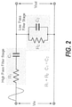
- the conventional RC network may be modeled as a series RC circuit connected to a parallel RC forming basically a High Pass Filter connected to a Low Pass Filter producing a very selective second-order frequency dependant band pass filter at the selected frequency (Fr).
- the reactance of the series capacitor (C1) is very high so it acts like an open circuit and blocks any input signal at V in . Therefore there is no output signal, V out .
- the reactance of the parallel capacitor, (C2) is very low so this parallel connected capacitor acts like a short circuit on the output so again there is no output signal.
- the output voltage reaches a maximum value with the frequency at which this happens being called the resonant frequency, (Fr).
- the magnitude of the output voltage is therefore at its maximum and is equal to one third (1/3) of the input voltage as shown in FIGs. 3A and 3B . It can be seen that at very low frequencies the phase angle between the input and output signals is "positive" (phase advanced), while at very high frequencies the phase angle becomes “negative” (phase delay). In the middle of these two points the circuit is at its resonant frequency, (fr) with the two signals being "in-phase” or 0°.
- the frequency selective RC network forms the basis of the Wien bridge oscillator circuit, where the RC network configured across a non-inverting amplifier as shown in FIG. 1 has a gain of 1+R1/R2.
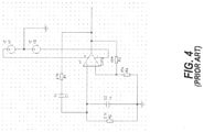
- FIG.4 a conventional Wien bridge oscillator, similar to that disclosed in FIG. 1 is disclosed, where illustrative resistive and capacitive values are shown.
- the Wien bridge oscillator starts oscillation at a gain of 3.13, which in turn saturates at peak voltages. This saturation may be seen in the magnified simulated waveform of FIG. 6 , where it can be seen in greater detail how the op-amp saturates at the peak voltages because the gain is greater than 3.
- a Wien bridge oscillator circuit 700 is disclosed under an illustrative embodiment that may be configured to be more reliable, produces less distortion in the output, and provides greater amplitude stability than conventional Wien bridge oscillators.
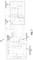
- the circuit 700 may be comprised of a Wien bridge oscillator circuit portion 702, an XY multiplier circuit portion 704, a full-wave rectifier circuit portion 706, an R-C filter circuit portion 708 and an integrator circuit portion 710. It should be appreciated by those skilled in the art that, while the illustration provides specific components and component values (e.g., resistors, capacitors, etc.), any alternate and/or additional components and component values may be used to perform the functions disclosed herein.
- Wien bridge oscillator circuit portion 702 comprises an operational amplifier X4 comprising a parallel RC network portion (e.g., R14, R17, R18, C6) coupled to the non-inverting input of amplifier X4, and to a series RC network portion (e.g., R13, R15, R16, C1), which is configured along a positive feedback path of amplifier X4 as shown in FIG. 7 .
- Wien bridge oscillator circuit 702 also includes a first negative feedback path through resistor R12 and a second negative feedback path via XY multiplier 704.
- XY multiplier 704 may be configured to multiply in a plurality of quadrants (e.g., (X 1 -X 2 )(Y 1 -Y 2 )/10V), divide in a plurality of quadrants (e.g., with a 10V Z/(X 1 -X 2 )), perform transfer functions and square roots in one quadrant (e.g., with a transfer function ⁇ 10 VZ ) .
- XY multiplier 704 is configured to receive Wien bridge oscillator circuit 702 output feedback at input n 1 and to receive a feedback output from integrator X1 of integrator circuit portion 710 at input n 2 .
- An illustrative, non-limiting example of full wave rectifier is shown in FIG. 8 , where a sine wave is provided in V1 , where a negative half-cycle is received via resistor R2 in an inverting (-) input of operational amplifier X1, while the positive half-cycle is passed through resistor R3 to non-inverting input of operational amplifier X2. As the non-inverting input of amplifier X1 is coupled to ground, amplifier X1 produces a positive output that is also coupled to the non-inverting input of operational amplifier X2.
- a differential integrator circuit portion 710 is coupled to the output of the full wave rectifier and the average of the full wave signal is compared to a 2.5 volt reference that may be produced by a programmable shunt regulator U1, whose reference terminal is coupled to a feedback output of integrator X1 via a series-parallel RC circuit (R8, R10, C4, C5) as shown in FIG. 7 .
- the output of the integrator X1 is fed to one input (n 2 ) of the XY multiplier 704.
- the integrator circuit portion 710 may be configured to compare and integrate a difference between the average voltage reference (2.5V) and the feedback average voltage of the full wave rectifier waveform.
- the n 1 input of the XY multiplier is connected to the output of the Wien bridge oscillator circuit portion 702.
- the output of the integrator circuit portion 710 multiplies the output of the Wien bridge oscillator, (e.g., a DC voltage times a sine wave), which may produce a controlled variable amplitude sine wave.
- the amplitude of the output sin wave is controlled because it has to satisfy the requirements of the integrator.
- FIG. 9 an illustrative, simulated output waveform for Wien bridge oscillator circuit 700 is shown. It can be seen from the non-limiting illustration that the peak voltage is controlled at 3.9V, and has no substantial distortion or saturation compared to the illustration of FIG. 6 .
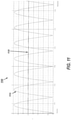
- FIG. 10 shows the sinusoidal voltage 1020 of the Wien bridge oscillator circuit 700 together with the voltage output 1010 of the full wave rectifier 706 which substantially produces a 3.9V peak on every positive and negative peak of the sinusoidal voltage 1020.
- FIG. 11 shows a full wave rectifier voltage output 1110 together with reference voltage of averaged full wave rectifier waveform (2.5V) and average value of the full wave output voltage (1120).
- Wien bridge oscillator Various operational characteristics of the Wien bridge oscillator disclosed herein have many advantageous applications in electronic circuitry. Some non-limiting operational characteristics of the Wien bridge oscillator include the dynamic gain control of the oscillator and the substantially "pure" sinusoidal waveform that is produced. In some illustrative, non-limiting embodiments, the present Wien bridge oscillator may be used as an input for voltage reference in power applications, such as synchronous-buck circuits (e.g., inverters, converters, etc.).
- synchronous-buck circuits e.g., inverters, converters, etc.
- Inverter 1200 comprises a DC source 1201 and a house supply 1202 for providing positive and negative voltages to high frequency switches A-B and low frequency switches C-D, as shown.
- switches A-D are comprised of high frequency switches, such as field effect transistors (FETs). It should be understood by those skilled in the art that other switches or suitable switching mechanisms may be employed, depending on the specific application of the inverter.
- Inverter 1200 may comprise a high frequency switching control (1) comprising controller 1203 and sensing circuit 1204.
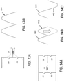
- controller may comprise a current-mode PWM controller (see FIG. 12C ) and sensing circuit 1204 comprises a peak current sense and an output voltage sense (see refs. 1204A-B of FIG. 4C).
- Controller 1203 may be operatively coupled to a gate of each of switches A-D, while sensing circuit 1204 may be coupled to a load line as is shown illustratively in FIG. 12A .
- controller may be a microprocessor running firmware to control switches A-D.
- Controller 1203 may be configured to provide a low frequency sine wave (or other suitable signal) to effect switching control on the synchronous-buck portion of inverter 1200.
- controller 1203 may utilize the Wien bridge oscillator 700 disclosed above.
- Main switching may be realized using synchronous-buck switching portion (2), comprising switches A and B, to invert every half cycle of the frequency of the signal provided by controller 1203. The inverting process thus creates a positive and negative transition of the sine wave signal.
- Low frequency switching stage (3) comprises switches C and D and may be configured to operate as zero voltage switching (ZVS) and zero current switching (ZCS) drives
- the charge on output capacitor 1205 is discharged to zero on every zero crossing of low frequency switching stage (3).
- the configuration of FIG. 12A advantageously discharges energy every half cycle. During this discharge of energy, the zero crossing distortion in the low frequency sine wave is greatly reduced.
- the fabricated switch material for synchronous-buck switching portion (2) e.g., switches A-B
- switches A-B may be different from the fabricated switch material for low frequency switching stage (3) (e.g., switches C-D).
- switches A-B may be fabricated on a Silicon Carbide (SiC) platform, which allows the switches to operate at higher frequencies and deliver higher circuit efficiencies.
- SiC switches have a reduced on state drain to source resistance (R ds(on) ), this improves on-state voltages and allows for higher power applications Since a SiC switch is a majority carrier device, there is no associated storage time to cause current tail issues within the switch.
- the SiC switch enables high voltage switching at higher frequencies (e.g., greater than 50kHz). Additionally, the total gate charge on a SiC switch is a multitude (e.g., 3 times) less than for a comparable silicon switch, resulting in yet further gains in the upper frequency limit and/or reduction of switching loss.
- SiC switches (A-B) in the synchronous-buck switching portion (2) numerous advantages may be achieved, including, but not limited to, improved switching, reduced harmonic distortion, reducing the need for large filters (e.g., inductors) at the output, and improved load step response.
- Gallium Nitride GaN
- GaN Gallium Nitride
- Similar advantages may be realized by using other high-frequency majority-carrier switches, such as Gallium Nitride (GaN), which also has a total gate charge that is a multitude (e.g., one-fifth) less than comparable silicon switches and reduced R ds(on) , allowing switching applications to exceed 2MHz in frequency and facilitating large step down ratios in the synchronous-buck switching portion (2).
- GaN Gallium Nitride
- switches A and B of the synchronous-buck switching portion (2) simultaneously and alternately provide high frequency PWM (x) and high frequency PWM complement (x') for each positive half wave and negative half wave.
- Switches C and D for the low frequency switching stage (3) are configured such that switch C is OFF for each positive half wave and ON for each negative half wave, while switch D is ON for each positive half wave and OFF for each negative half wave.
- FIG. 12C is another exemplary embodiment of a synchronous buck inverter, similar to inverter 1200, wherein high voltage regulator house supply 1202 receives input power (+HV, -HV) from a source (e.g., 1201) and produces output voltage +V for each of the switch drives (A-D Drive) and voltage +VL for current-mode PWM controller 1203, peak current sense 1204A and output voltage sense 1204B.
- Controller 1203 may provide low frequency signals (e.g., sine wave) via low frequency oscillator 1210, which may utilize the Wien bridge oscillator 700 disclosed above. Controller 1203 as illustrated in the embodiment of FIG.
- HF switching portion may activate a high frequency (HF) switching portion and low frequency (LF) switching portion, wherein HF switching portion activates/deactivates switches associated with A DRIVE and B DRIVE of synchronous-buck/buck-synchronous stage 1211 (see section (2) of FIG. 4A).
- LF switching portion may activate/deactivate switches associated with C DRIVE and D DRIVE of inverter stage 1212 (see section (3) of FIG. 4A).
- the PWM controller 1203 may be coupled to a dithering circuit 1214 which may be configured to apply a waveform to a timing circuit of controller 1203 to dither the switching frequency.
- a triangular waveform may be applied to a timing circuit of controller 1203 to cause the frequency to change a certain amount (e.g., ⁇ 10kHz) for a given switching frequency (e.g., 100kHz).
- a triangular waveform (e.g., 2-3V peak) may be applied for ⁇ 8kHz dithering to a timing circuit to cause the frequency to change a certain amount for a given switching frequency.
- the switching frequency dither increases to 108kHz at a peak, and decreases to 92kHz at a zero crossing.
- an inverter performance may be improved by increasing resolution and decreasing harmonic distortion.
- suitable dithering frequency ranges may be used, and are not limited to the specific example.
- conventional synchronous buck converters typically rely on an H-Bridge topology and a single-polar or double-polar switching scheme to produce a steady DC output voltage.
- such configurations are subject to high power losses.
- conventional configurations rely on the load to pull the voltage down to zero, this may further introduce significant harmonic distortions, particularly with small loads.
- the technologies and techniques described herein may be used for a synchronous buck converter to produce a steady DC output voltage.
- the synchronous switches S1 and S2 of the simplified figure may be configured as high frequency switches to have on/off states (an "on" state illustrated as dotted line in the figure) to cause current to flow through inductor L1 (illustrated as dotted line arrows in the figure) to produce a varying rectified sinusoid shown in FIG. 5B.
- low frequency switches may be added to the circuit of FIG. 5A.
- low-frequency switches S3 and S4 are added as shown in the simplified embodiment, and are configured to synchronously switch with switches S1 and S2 to actively pull down voltage to produce waveforms illustrated in FIG. 6B and FIG. 6C.
- the switching of S3 and S4 is configured to "un-fold" or invert a portion 1200 of the rectified signal 1210 (in the direction of the arrow as shown) to produce a sine wave illustrated in FIG. 6C comprising signal 1210 and inverted portion 1220.
- switches S1 and S2 may be fabricated from SiC or GaN (discussed above in connection with FIG. 3A ) to provide further advantageous switching and circuit response properties.
- reduced harmonic distortion may be advantageously achieved. With better control over harmonic distortion, bulky, low-frequency output inductors may be significantly reduced. Moreover, the disclosed configurations are much more responsive to load changes.
Landscapes
- Engineering & Computer Science (AREA)
- Power Engineering (AREA)
- Inverter Devices (AREA)
- Inductance-Capacitance Distribution Constants And Capacitance-Resistance Oscillators (AREA)
Claims (7)
- Oszillatorschaltung (700), umfassend:eine Wien-Brücke-Oszillatorschaltung (702);eine Vollwellengleichrichterschaltung (706), die mit einem Ausgang der Wien-Brücke-Oszillatorschaltung (702) gekoppelt ist;eine Integratorschaltung (710), die mit einem Ausgang der Vollwellengleichrichterschaltung gekoppelt ist; undeine Vervielfacherschaltung (704), umfassend einen ersten Eingang, der mit dem Ausgang der Wien-Brücke-Oszillatorschaltung (702) gekoppelt ist, und einen zweiten Eingang, der mit einem Ausgang der Integratorschaltung (710) gekoppelt ist, wobei die Vervielfacherschaltung (704) dazu konfiguriert ist, ein Signal für einen Eingang der Wien-Brücke-Oszillatorschaltung (702) bereitzustellen,wobei der Vollwellengleichrichter (706) dazu konfiguriert ist, eine Übertragungsfunktion an der Spannung auszuführen, die an einem ersten Eingang, der mit dem Ausgang der Wien-Brücke-Oszillatorschaltung (702) gekoppelt ist, empfangen wird,wobei der Vollwellengleichrichter (706) konfiguriert ist zum Ausführen der Übertragungsfunktion VOUT gemäß
 wobei V(n1) ein an dem ersten Eingang des Vollwellengleichrichters (706) empfangener Spannungsausgang des Wien-Brücke-Oszillators ist,wobei die Oszillatorschaltung ferner eine RC-Schaltung (708) umfasst, die zwischen dem Ausgang der Vollwellengleichrichterschaltung (706) und der Integratorschaltung (710) gekoppelt ist, wobei die Vollwellengleichrichterschaltung (706) Schaltkreise zur Ermöglichung der Übertragungsfunktion an dem Ausgang der Wien-Brücke-Oszillatorschaltung (702) und zur Bereitstellung des Ausgangs für die RC-Schaltung (708) umfasst und in der Vollwellengleichrichterschaltung (706) eine Sinuswelle bereitgestellt wird, eine negative Halbwelle über einen zweiten Widerstand (R2) in dem invertierenden (-) Eingang eines ersten Operationsverstärkers (X1) empfangen wird, während eine positive Halbwelle durch einen dritten Widerstand (R3) zu dem nicht-invertierenden Eingang eines zweiten Operationsverstärkers (X2) geführt wird, und der erste Operationsverstärker (X1) dazu konfiguriert ist, einen positiven Ausgang zu erzeugen, der ebenfalls mit dem nicht-invertierenden Eingang des zweiten Operationsverstärkers (X2) gekoppelt ist, und wobei der nicht-invertierende Eingang des ersten Operationsverstärkers (X1) über einen ersten Widerstand (R1) mit Masse gekoppelt ist, wobei die Wien-Brücke-Oszillatorschaltung (702) einen vierten Operationsverstärker (X4) umfasst, welcher einen zwischen der Masse und dem nicht-invertierenden Eingang des vierten Operationsverstärkers (X4) gekoppelten parallelen RC-Netzwerkabschnitt (R14, R17, R18, C6), einen zwischen dem Ausgangsanschluss und dem nicht-invertierenden Eingangsanschluss des vierten Operationsverstärkers (X4) geschalteten seriellen RC-Netzwerkabschnitt (R13, R15, R16, C1) und einen zwölften Widerstand (R12), der zwischen dem Ausgangsanschluss und dem invertierenden Eingangsanschluss des vierten Operationsverstärkers (X4) geschaltet ist, umfasst, wobei der Ausgang der Vervielfacherschaltung (704) mit dem negativen Eingangsanschluss des vierten Operationsverstärkers (X4) verbunden ist, wobei die RC-Schaltung (708) Widerstände (R6-R7) und Kondensatoren (C2-C3) umfasst, wobei die Integratorschaltung (710), die mit dem Ausgang der Vollwellengleichrichterschaltung (706) gekoppelt ist, dazu konfiguriert ist, den Mittelwert eines Vollwellensignals mit einer 2,5-Volt-Referenz zu vergleichen, die von einem programmierbaren Querregler (U1) erzeugt wird, dessen Referenzanschluss über eine seriellparallele RC-Schaltung (R8, R10, C4, C5) mit dem Ausgangsanschluss des Integrators (710) gekoppelt ist.
 - Oszillatorschaltung nach Anspruch 1, wobei die Vervielfacherschaltung einen XY-Vervielfacher (704) umfasst.
- Oszillatorschaltung nach Anspruch 2, wobei die Vervielfacherschaltung (704) dazu konfiguriert ist, eine Übertragungsfunktion an Spannung auszuführen, die an dem ersten Eingang und dem zweiten Eingang empfangen wird.
- Oszillatorschaltung nach einem der Ansprüche 2-3, wobei die Vervielfacherschaltung konfiguriert ist zum Ausführen der Übertragungsfunktion VOUT gemäß

- Oszillatorschaltung nach einem der Ansprüche 1-4, wobei die Wien-Brücke-Oszillatorschaltung (702) zum Erzeugen eines Signals konfiguriert ist; die Vollwellengleichrichterschaltung (706) zum Gleichrichten des erzeugten Signals konfiguriert ist; die Integratorschaltung (710) zum Integrieren des gleichgerichteten erzeugten Signals konfiguriert ist und die Vervielfacherschaltung (704) zum dynamischen Steuern der Verstärkung in der Wien-Brücke-Oszillatorschaltung konfiguriert ist.
- Oszillatorschaltung nach einem der Ansprüche 1-5, wobei ein Ausgang der Integratorschaltung (710) mit einer synchronen Abwärtsschaltung gekoppelt ist.
- Oszillatorschaltung nach Anspruch 6, wobei die Integratorschaltung (710) dazu konfiguriert ist, für die synchrone Abwärtsschaltung ein sinusförmiges Referenzsignal bereitzustellen.
Applications Claiming Priority (3)
| Application Number | Priority Date | Filing Date | Title |
|---|---|---|---|
| US201462047443P | 2014-09-08 | 2014-09-08 | |
| US14/675,073 US9647608B2 (en) | 2014-09-08 | 2015-03-31 | Wein bridge oscillator |
| PCT/US2015/048989 WO2016040350A1 (en) | 2014-09-08 | 2015-09-08 | Wien bridge oscillator circuit |
Publications (3)
| Publication Number | Publication Date |
|---|---|
| EP3192168A1 EP3192168A1 (de) | 2017-07-19 |
| EP3192168A4 EP3192168A4 (de) | 2018-05-16 |
| EP3192168B1 true EP3192168B1 (de) | 2022-03-16 |
Family
ID=55438447
Family Applications (2)
| Application Number | Title | Priority Date | Filing Date |
|---|---|---|---|
| EP15840810.4A Ceased EP3192160A4 (de) | 2014-09-08 | 2015-09-08 | Synchroner abwärtswechselrichter |
| EP15839315.7A Active EP3192168B1 (de) | 2014-09-08 | 2015-09-08 | Wien-brücke-oszillatorschaltung |
Family Applications Before (1)
| Application Number | Title | Priority Date | Filing Date |
|---|---|---|---|
| EP15840810.4A Ceased EP3192160A4 (de) | 2014-09-08 | 2015-09-08 | Synchroner abwärtswechselrichter |
Country Status (3)
| Country | Link |
|---|---|
| US (6) | US9660580B2 (de) |
| EP (2) | EP3192160A4 (de) |
| WO (2) | WO2016040319A1 (de) |
Families Citing this family (10)
| Publication number | Priority date | Publication date | Assignee | Title |
|---|---|---|---|---|
| US9917515B2 (en) * | 2014-06-24 | 2018-03-13 | Technische Universiteit Eindhoven | Cascadable modular 4-switch extended commutation cell |
| US9660580B2 (en) * | 2014-09-08 | 2017-05-23 | Jabil Circuit, Inc. | Synchronous buck inverter |
| US10050561B2 (en) * | 2016-12-30 | 2018-08-14 | Sunpower Corporation | Three-level inverter switching |
| CN110149069A (zh) * | 2019-04-30 | 2019-08-20 | 国网江苏省电力有限公司电力科学研究院 | 高效率高频逆变电路 |
| CN110879337A (zh) * | 2019-11-06 | 2020-03-13 | 广州供电局有限公司 | 震荡波电压产生电路及电缆局部放电检测装置 |
| US11048361B1 (en) | 2020-04-09 | 2021-06-29 | Alps Alpine Co., Ltd. | Systems and methods to create offset signal using sinewave generator with programmable amplitude and phase |
| CN112202357B (zh) * | 2020-12-09 | 2021-03-09 | 深圳市尚科新能源有限公司 | 一种spwm调制方法 |
| US12430100B2 (en) | 2021-06-01 | 2025-09-30 | Ceremorphic, Inc. | Analog multiplier accumulator with unit element gain balancing |
| US12462150B2 (en) | 2021-10-31 | 2025-11-04 | Ceremorphic, Inc. | Modular analog multiplier-accumulator unit element for multi-layer neural networks |
| CN114123184A (zh) * | 2021-11-25 | 2022-03-01 | 国网四川省电力公司经济技术研究院 | 一种基于逆变器端口能量函数的控制系统及控制方法 |
Family Cites Families (35)
| Publication number | Priority date | Publication date | Assignee | Title |
|---|---|---|---|---|
| US3835418A (en) * | 1972-10-17 | 1974-09-10 | Rfl Ind Inc | Stabilized alternating current source |
| US4131937A (en) * | 1976-05-14 | 1978-12-26 | Electric Power Research Institute, Inc. | Naturally commutated voltage-fed converter for linking a DC source to an AC system |
| US4542353A (en) | 1983-12-05 | 1985-09-17 | General Electric Company | Sine wave generator |
| JPS60200770A (ja) * | 1984-03-23 | 1985-10-11 | Meidensha Electric Mfg Co Ltd | 正弦波インバ−タ |
| JPH04236171A (ja) * | 1991-01-21 | 1992-08-25 | Meidensha Corp | インバータの出力電圧波形歪み抑制法 |
| US5277495A (en) | 1992-04-24 | 1994-01-11 | Halliburton Company | Temperature to frequency converter |
| DE69409968T2 (de) * | 1993-11-30 | 1998-10-29 | Crown International, Inc., Elkhart, Ind. | Schaltnetzteil für einen leistungsverstärker |
| JP2914251B2 (ja) * | 1995-10-31 | 1999-06-28 | 日本電気株式会社 | インバータ装置 |
| US5734258A (en) * | 1996-06-03 | 1998-03-31 | General Electric Company | Bidirectional buck boost converter |
| JP3234909B2 (ja) * | 1996-12-13 | 2001-12-04 | シャープ株式会社 | インバータ制御装置、およびインバータの制御方法 |
| US6144172A (en) | 1999-05-14 | 2000-11-07 | Matsushita Electric Works R&D Laboratory, Inc. | Method and driving circuit for HID lamp electronic ballast |
| US6147886A (en) * | 1999-05-15 | 2000-11-14 | Technical Witts, Inc. | Dual opposed interleaved coupled inductor soft switching converters |
| US6377163B1 (en) | 2000-09-21 | 2002-04-23 | Home Touch Lighting Systems Llc | Power line communication circuit |
| US6593703B2 (en) | 2001-06-15 | 2003-07-15 | Matsushita Electric Works, Ltd. | Apparatus and method for driving a high intensity discharge lamp |
| CA2458654A1 (en) | 2001-08-30 | 2003-03-13 | William L. Stewart | Power management method and system |
| AU2003220665A1 (en) * | 2002-04-03 | 2003-10-20 | International Rectifier Corporation | Synchronous buck converter improvements |
| US6643145B1 (en) | 2002-07-26 | 2003-11-04 | Intersil Americas Inc. | High resolution digital diode emulator for DC-DC converters |
| US8204709B2 (en) | 2005-01-18 | 2012-06-19 | Solar Sentry Corporation | System and method for monitoring photovoltaic power generation systems |
| US7385375B2 (en) * | 2005-02-23 | 2008-06-10 | Coldwatt, Inc. | Control circuit for a depletion mode switch and method of operating the same |
| WO2007041693A2 (en) | 2005-10-04 | 2007-04-12 | Thompson Technology Industries, Inc. | System and method for array and string level monitoring of a grid-connected photovoltaic power system |
| CN100481710C (zh) * | 2006-01-23 | 2009-04-22 | 艾默生网络能源有限公司 | 一种正弦基准电路 |
| JP4783294B2 (ja) | 2006-02-27 | 2011-09-28 | 三菱電機株式会社 | 系統連系用電力変換装置 |
| GB0725316D0 (en) | 2007-12-28 | 2008-02-06 | Nokia Corp | A controller |
| US7929325B2 (en) | 2008-05-27 | 2011-04-19 | General Electric Company | High efficiency, multi-source photovoltaic inverter |
| EP2144356B1 (de) * | 2008-07-09 | 2019-06-26 | Dialog Semiconductor GmbH | Abwärtswandlerschwellenerkennung für einen automatischen Impulsüberspringungsmodus |
| US8378656B2 (en) * | 2008-09-19 | 2013-02-19 | General Electric Company | Quasi-AC, photovoltaic module for unfolder photovoltaic inverter |
| US20120155139A1 (en) | 2009-09-07 | 2012-06-21 | Koninklijke Philips Electronics N.V. | Electrical Energy Conversion Circuit Device |
| US8294418B2 (en) | 2010-02-03 | 2012-10-23 | ConvenientPower, Ltd. | Power transfer device and method |
| US8488350B2 (en) | 2009-09-25 | 2013-07-16 | Astec International Limited | DC-AC inverters |
| US8773102B2 (en) | 2011-01-03 | 2014-07-08 | Eta Semiconductor Inc. | Hysteretic CL power converter |
| CN103001526B (zh) | 2011-09-15 | 2015-09-02 | 南京博兰得电子科技有限公司 | 一种非隔离型逆变器及其控制方法 |
| US9112383B2 (en) | 2011-10-31 | 2015-08-18 | General Electric Company | System and method for Var injection at a distributed power generation source |
| US8988054B2 (en) | 2011-12-27 | 2015-03-24 | St-Ericsson Sa | Single feedback loop for parallel architecture buck converter—LDO regulator |
| US20130229215A1 (en) * | 2012-03-02 | 2013-09-05 | Laurence P. Sadwick | Variable Resistance for Driver Circuit Dithering |
| US9660580B2 (en) * | 2014-09-08 | 2017-05-23 | Jabil Circuit, Inc. | Synchronous buck inverter |
-
2015
- 2015-03-31 US US14/674,993 patent/US9660580B2/en active Active
- 2015-03-31 US US14/675,073 patent/US9647608B2/en active Active
- 2015-09-08 WO PCT/US2015/048934 patent/WO2016040319A1/en not_active Ceased
- 2015-09-08 WO PCT/US2015/048989 patent/WO2016040350A1/en not_active Ceased
- 2015-09-08 EP EP15840810.4A patent/EP3192160A4/de not_active Ceased
- 2015-09-08 EP EP15839315.7A patent/EP3192168B1/de active Active
-
2016
- 2016-08-30 US US15/251,487 patent/US9935580B2/en active Active
-
2017
- 2017-10-04 US US15/724,839 patent/US10840824B2/en active Active
-
2020
- 2020-10-13 US US17/069,459 patent/US11336204B2/en active Active
-
2022
- 2022-05-16 US US17/744,895 patent/US12249927B2/en active Active
Non-Patent Citations (2)
| Title |
|---|
| ANONYMOUS: "Square root - Wikipedia", 23 September 2014 (2014-09-23), pages 1 - 13, XP055798261, Retrieved from the Internet <URL:https://en.wikipedia.org/w/index.php?title=Square_root&oldid=626796579> [retrieved on 20210422] * |
| KUHN KENNETH A: "Precision Diode Rectifiers 1", 21 March 2013 (2013-03-21), pages 1 - 7, XP055798257, Retrieved from the Internet <URL:http://www.kennethkuhn.com/students/ee431/precision_diode_rectifiers.pdf> [retrieved on 20210422] * |
Also Published As
| Publication number | Publication date |
|---|---|
| US11336204B2 (en) | 2022-05-17 |
| US20180097477A1 (en) | 2018-04-05 |
| EP3192160A4 (de) | 2018-03-28 |
| EP3192168A4 (de) | 2018-05-16 |
| EP3192160A1 (de) | 2017-07-19 |
| US9660580B2 (en) | 2017-05-23 |
| US12249927B2 (en) | 2025-03-11 |
| WO2016040350A1 (en) | 2016-03-17 |
| US9647608B2 (en) | 2017-05-09 |
| US10840824B2 (en) | 2020-11-17 |
| US9935580B2 (en) | 2018-04-03 |
| US20220352830A1 (en) | 2022-11-03 |
| US20160072404A1 (en) | 2016-03-10 |
| WO2016040319A1 (en) | 2016-03-17 |
| US20210028723A1 (en) | 2021-01-28 |
| US20160373059A1 (en) | 2016-12-22 |
| US20160072437A1 (en) | 2016-03-10 |
| EP3192168A1 (de) | 2017-07-19 |
Similar Documents
| Publication | Publication Date | Title |
|---|---|---|
| EP3192168B1 (de) | Wien-brücke-oszillatorschaltung | |
| JP6571718B2 (ja) | 高周波電源 | |
| CN107112921B (zh) | 电网耦合逆变器、逆变器装置和用于逆变器装置的运行方法 | |
| EP3379678A1 (de) | Ausgleicherschaltung | |
| CN111884507B (zh) | 一种用于功率变换器的控制电路及其控制方法 | |
| WO2016149322A1 (en) | Midpoint control and gain scheduling for power converters | |
| TWI886613B (zh) | 飛跨電容多電平整流器及其控制方法 | |
| CN107017762A (zh) | 一种直流电容器谐波电流抑制方法 | |
| CN105981280A (zh) | 电力变换装置 | |
| Pantic et al. | Inductive power transfer by means of multiple frequencies in the magnetic link | |
| Zahira et al. | SPWM technique for reducing harmonics in three-phase non-linear load | |
| RU2459342C1 (ru) | Резонансный преобразователь постоянного напряжения в постоянное и переменное и способ управления его выходным напряжением | |
| Shenkman et al. | Improved modification of the single-switch AC-AC converter for induction heating applications | |
| Calinin et al. | Investigation of the possibilities of increasing the frequency converter efficiency based on the phase-shift transformer | |
| JP6397772B2 (ja) | インバータ装置 | |
| JP4815996B2 (ja) | 電力変換装置 | |
| Gerardo et al. | Interconnection and damping passivity-based control applied to a single-phase voltage source inverter | |
| Kanaan et al. | DC load unbalance and mains disturbances effects on a three-phase three-switch three-level boost rectifier | |
| JP6154158B2 (ja) | スイッチングレギュレータ | |
| Ekhtiari et al. | Digitized self-oscillating loop for piezoelectric transformer-based power converters | |
| RU2305890C2 (ru) | Способ управления работой м-фазного регулятора-преобразователя переменно-переменного тока | |
| RU91485U1 (ru) | Трехфазный преобразователь частоты | |
| CN114915159A (zh) | 一种功率因数校正整流器 | |
| SU1150709A1 (ru) | Способ управлени регул тором напр жени | |
| Matias et al. | Steady state analysis of separated dc-link universal power line conditioner |
Legal Events
| Date | Code | Title | Description |
|---|---|---|---|
| STAA | Information on the status of an ep patent application or granted ep patent |
Free format text: STATUS: THE INTERNATIONAL PUBLICATION HAS BEEN MADE |
|
| PUAI | Public reference made under article 153(3) epc to a published international application that has entered the european phase |
Free format text: ORIGINAL CODE: 0009012 |
|
| STAA | Information on the status of an ep patent application or granted ep patent |
Free format text: STATUS: REQUEST FOR EXAMINATION WAS MADE |
|
| 17P | Request for examination filed |
Effective date: 20170405 |
|
| AK | Designated contracting states |
Kind code of ref document: A1 Designated state(s): AL AT BE BG CH CY CZ DE DK EE ES FI FR GB GR HR HU IE IS IT LI LT LU LV MC MK MT NL NO PL PT RO RS SE SI SK SM TR |
|
| AX | Request for extension of the european patent |
Extension state: BA ME |
|
| DAV | Request for validation of the european patent (deleted) | ||
| DAX | Request for extension of the european patent (deleted) | ||
| RAP1 | Party data changed (applicant data changed or rights of an application transferred) |
Owner name: JABIL INC. |
|
| A4 | Supplementary search report drawn up and despatched |
Effective date: 20180413 |
|
| RIC1 | Information provided on ipc code assigned before grant |
Ipc: H02M 7/5387 20070101ALI20180409BHEP Ipc: H02M 1/00 20060101ALI20180409BHEP Ipc: H02M 7/48 20070101ALI20180409BHEP Ipc: H03B 5/22 20060101ALI20180409BHEP Ipc: H03B 5/26 20060101AFI20180409BHEP Ipc: H03B 5/10 20060101ALI20180409BHEP Ipc: H02M 3/158 20060101ALI20180409BHEP |
|
| STAA | Information on the status of an ep patent application or granted ep patent |
Free format text: STATUS: EXAMINATION IS IN PROGRESS |
|
| 17Q | First examination report despatched |
Effective date: 20200226 |
|
| GRAP | Despatch of communication of intention to grant a patent |
Free format text: ORIGINAL CODE: EPIDOSNIGR1 |
|
| STAA | Information on the status of an ep patent application or granted ep patent |
Free format text: STATUS: GRANT OF PATENT IS INTENDED |
|
| INTG | Intention to grant announced |
Effective date: 20211006 |
|
| GRAS | Grant fee paid |
Free format text: ORIGINAL CODE: EPIDOSNIGR3 |
|
| GRAA | (expected) grant |
Free format text: ORIGINAL CODE: 0009210 |
|
| STAA | Information on the status of an ep patent application or granted ep patent |
Free format text: STATUS: THE PATENT HAS BEEN GRANTED |
|
| AK | Designated contracting states |
Kind code of ref document: B1 Designated state(s): AL AT BE BG CH CY CZ DE DK EE ES FI FR GB GR HR HU IE IS IT LI LT LU LV MC MK MT NL NO PL PT RO RS SE SI SK SM TR |
|
| REG | Reference to a national code |
Ref country code: GB Ref legal event code: FG4D |
|
| REG | Reference to a national code |
Ref country code: CH Ref legal event code: EP |
|
| REG | Reference to a national code |
Ref country code: DE Ref legal event code: R096 Ref document number: 602015077615 Country of ref document: DE |
|
| REG | Reference to a national code |
Ref country code: IE Ref legal event code: FG4D |
|
| REG | Reference to a national code |
Ref country code: AT Ref legal event code: REF Ref document number: 1476599 Country of ref document: AT Kind code of ref document: T Effective date: 20220415 |
|
| REG | Reference to a national code |
Ref country code: LT Ref legal event code: MG9D |
|
| REG | Reference to a national code |
Ref country code: NL Ref legal event code: MP Effective date: 20220316 |
|
| PG25 | Lapsed in a contracting state [announced via postgrant information from national office to epo] |
Ref country code: SE Free format text: LAPSE BECAUSE OF FAILURE TO SUBMIT A TRANSLATION OF THE DESCRIPTION OR TO PAY THE FEE WITHIN THE PRESCRIBED TIME-LIMIT Effective date: 20220316 Ref country code: RS Free format text: LAPSE BECAUSE OF FAILURE TO SUBMIT A TRANSLATION OF THE DESCRIPTION OR TO PAY THE FEE WITHIN THE PRESCRIBED TIME-LIMIT Effective date: 20220316 Ref country code: NO Free format text: LAPSE BECAUSE OF FAILURE TO SUBMIT A TRANSLATION OF THE DESCRIPTION OR TO PAY THE FEE WITHIN THE PRESCRIBED TIME-LIMIT Effective date: 20220616 Ref country code: LT Free format text: LAPSE BECAUSE OF FAILURE TO SUBMIT A TRANSLATION OF THE DESCRIPTION OR TO PAY THE FEE WITHIN THE PRESCRIBED TIME-LIMIT Effective date: 20220316 Ref country code: HR Free format text: LAPSE BECAUSE OF FAILURE TO SUBMIT A TRANSLATION OF THE DESCRIPTION OR TO PAY THE FEE WITHIN THE PRESCRIBED TIME-LIMIT Effective date: 20220316 Ref country code: BG Free format text: LAPSE BECAUSE OF FAILURE TO SUBMIT A TRANSLATION OF THE DESCRIPTION OR TO PAY THE FEE WITHIN THE PRESCRIBED TIME-LIMIT Effective date: 20220616 |
|
| REG | Reference to a national code |
Ref country code: AT Ref legal event code: MK05 Ref document number: 1476599 Country of ref document: AT Kind code of ref document: T Effective date: 20220316 |
|
| PG25 | Lapsed in a contracting state [announced via postgrant information from national office to epo] |
Ref country code: LV Free format text: LAPSE BECAUSE OF FAILURE TO SUBMIT A TRANSLATION OF THE DESCRIPTION OR TO PAY THE FEE WITHIN THE PRESCRIBED TIME-LIMIT Effective date: 20220316 Ref country code: GR Free format text: LAPSE BECAUSE OF FAILURE TO SUBMIT A TRANSLATION OF THE DESCRIPTION OR TO PAY THE FEE WITHIN THE PRESCRIBED TIME-LIMIT Effective date: 20220617 Ref country code: FI Free format text: LAPSE BECAUSE OF FAILURE TO SUBMIT A TRANSLATION OF THE DESCRIPTION OR TO PAY THE FEE WITHIN THE PRESCRIBED TIME-LIMIT Effective date: 20220316 |
|
| PG25 | Lapsed in a contracting state [announced via postgrant information from national office to epo] |
Ref country code: NL Free format text: LAPSE BECAUSE OF FAILURE TO SUBMIT A TRANSLATION OF THE DESCRIPTION OR TO PAY THE FEE WITHIN THE PRESCRIBED TIME-LIMIT Effective date: 20220316 |
|
| PG25 | Lapsed in a contracting state [announced via postgrant information from national office to epo] |
Ref country code: SM Free format text: LAPSE BECAUSE OF FAILURE TO SUBMIT A TRANSLATION OF THE DESCRIPTION OR TO PAY THE FEE WITHIN THE PRESCRIBED TIME-LIMIT Effective date: 20220316 Ref country code: SK Free format text: LAPSE BECAUSE OF FAILURE TO SUBMIT A TRANSLATION OF THE DESCRIPTION OR TO PAY THE FEE WITHIN THE PRESCRIBED TIME-LIMIT Effective date: 20220316 Ref country code: RO Free format text: LAPSE BECAUSE OF FAILURE TO SUBMIT A TRANSLATION OF THE DESCRIPTION OR TO PAY THE FEE WITHIN THE PRESCRIBED TIME-LIMIT Effective date: 20220316 Ref country code: PT Free format text: LAPSE BECAUSE OF FAILURE TO SUBMIT A TRANSLATION OF THE DESCRIPTION OR TO PAY THE FEE WITHIN THE PRESCRIBED TIME-LIMIT Effective date: 20220718 Ref country code: ES Free format text: LAPSE BECAUSE OF FAILURE TO SUBMIT A TRANSLATION OF THE DESCRIPTION OR TO PAY THE FEE WITHIN THE PRESCRIBED TIME-LIMIT Effective date: 20220316 Ref country code: EE Free format text: LAPSE BECAUSE OF FAILURE TO SUBMIT A TRANSLATION OF THE DESCRIPTION OR TO PAY THE FEE WITHIN THE PRESCRIBED TIME-LIMIT Effective date: 20220316 Ref country code: CZ Free format text: LAPSE BECAUSE OF FAILURE TO SUBMIT A TRANSLATION OF THE DESCRIPTION OR TO PAY THE FEE WITHIN THE PRESCRIBED TIME-LIMIT Effective date: 20220316 Ref country code: AT Free format text: LAPSE BECAUSE OF FAILURE TO SUBMIT A TRANSLATION OF THE DESCRIPTION OR TO PAY THE FEE WITHIN THE PRESCRIBED TIME-LIMIT Effective date: 20220316 |
|
| PG25 | Lapsed in a contracting state [announced via postgrant information from national office to epo] |
Ref country code: PL Free format text: LAPSE BECAUSE OF FAILURE TO SUBMIT A TRANSLATION OF THE DESCRIPTION OR TO PAY THE FEE WITHIN THE PRESCRIBED TIME-LIMIT Effective date: 20220316 Ref country code: IS Free format text: LAPSE BECAUSE OF FAILURE TO SUBMIT A TRANSLATION OF THE DESCRIPTION OR TO PAY THE FEE WITHIN THE PRESCRIBED TIME-LIMIT Effective date: 20220716 Ref country code: AL Free format text: LAPSE BECAUSE OF FAILURE TO SUBMIT A TRANSLATION OF THE DESCRIPTION OR TO PAY THE FEE WITHIN THE PRESCRIBED TIME-LIMIT Effective date: 20220316 |
|
| REG | Reference to a national code |
Ref country code: DE Ref legal event code: R097 Ref document number: 602015077615 Country of ref document: DE |
|
| PLBE | No opposition filed within time limit |
Free format text: ORIGINAL CODE: 0009261 |
|
| STAA | Information on the status of an ep patent application or granted ep patent |
Free format text: STATUS: NO OPPOSITION FILED WITHIN TIME LIMIT |
|
| PG25 | Lapsed in a contracting state [announced via postgrant information from national office to epo] |
Ref country code: DK Free format text: LAPSE BECAUSE OF FAILURE TO SUBMIT A TRANSLATION OF THE DESCRIPTION OR TO PAY THE FEE WITHIN THE PRESCRIBED TIME-LIMIT Effective date: 20220316 |
|
| 26N | No opposition filed |
Effective date: 20221219 |
|
| PG25 | Lapsed in a contracting state [announced via postgrant information from national office to epo] |
Ref country code: SI Free format text: LAPSE BECAUSE OF FAILURE TO SUBMIT A TRANSLATION OF THE DESCRIPTION OR TO PAY THE FEE WITHIN THE PRESCRIBED TIME-LIMIT Effective date: 20220316 |
|
| PG25 | Lapsed in a contracting state [announced via postgrant information from national office to epo] |
Ref country code: MC Free format text: LAPSE BECAUSE OF FAILURE TO SUBMIT A TRANSLATION OF THE DESCRIPTION OR TO PAY THE FEE WITHIN THE PRESCRIBED TIME-LIMIT Effective date: 20220316 |
|
| REG | Reference to a national code |
Ref country code: CH Ref legal event code: PL |
|
| REG | Reference to a national code |
Ref country code: BE Ref legal event code: MM Effective date: 20220930 |
|
| P01 | Opt-out of the competence of the unified patent court (upc) registered |
Effective date: 20230524 |
|
| PG25 | Lapsed in a contracting state [announced via postgrant information from national office to epo] |
Ref country code: LU Free format text: LAPSE BECAUSE OF NON-PAYMENT OF DUE FEES Effective date: 20220908 |
|
| PG25 | Lapsed in a contracting state [announced via postgrant information from national office to epo] |
Ref country code: LI Free format text: LAPSE BECAUSE OF NON-PAYMENT OF DUE FEES Effective date: 20220930 Ref country code: IT Free format text: LAPSE BECAUSE OF FAILURE TO SUBMIT A TRANSLATION OF THE DESCRIPTION OR TO PAY THE FEE WITHIN THE PRESCRIBED TIME-LIMIT Effective date: 20220316 Ref country code: IE Free format text: LAPSE BECAUSE OF NON-PAYMENT OF DUE FEES Effective date: 20220908 Ref country code: CH Free format text: LAPSE BECAUSE OF NON-PAYMENT OF DUE FEES Effective date: 20220930 |
|
| PG25 | Lapsed in a contracting state [announced via postgrant information from national office to epo] |
Ref country code: BE Free format text: LAPSE BECAUSE OF NON-PAYMENT OF DUE FEES Effective date: 20220930 |
|
| PG25 | Lapsed in a contracting state [announced via postgrant information from national office to epo] |
Ref country code: HU Free format text: LAPSE BECAUSE OF FAILURE TO SUBMIT A TRANSLATION OF THE DESCRIPTION OR TO PAY THE FEE WITHIN THE PRESCRIBED TIME-LIMIT; INVALID AB INITIO Effective date: 20150908 |
|
| PG25 | Lapsed in a contracting state [announced via postgrant information from national office to epo] |
Ref country code: CY Free format text: LAPSE BECAUSE OF FAILURE TO SUBMIT A TRANSLATION OF THE DESCRIPTION OR TO PAY THE FEE WITHIN THE PRESCRIBED TIME-LIMIT Effective date: 20220316 |
|
| PG25 | Lapsed in a contracting state [announced via postgrant information from national office to epo] |
Ref country code: MK Free format text: LAPSE BECAUSE OF FAILURE TO SUBMIT A TRANSLATION OF THE DESCRIPTION OR TO PAY THE FEE WITHIN THE PRESCRIBED TIME-LIMIT Effective date: 20220316 |
|
| PG25 | Lapsed in a contracting state [announced via postgrant information from national office to epo] |
Ref country code: TR Free format text: LAPSE BECAUSE OF FAILURE TO SUBMIT A TRANSLATION OF THE DESCRIPTION OR TO PAY THE FEE WITHIN THE PRESCRIBED TIME-LIMIT Effective date: 20220316 |
|
| PG25 | Lapsed in a contracting state [announced via postgrant information from national office to epo] |
Ref country code: MT Free format text: LAPSE BECAUSE OF FAILURE TO SUBMIT A TRANSLATION OF THE DESCRIPTION OR TO PAY THE FEE WITHIN THE PRESCRIBED TIME-LIMIT Effective date: 20220316 |
|
| PGFP | Annual fee paid to national office [announced via postgrant information from national office to epo] |
Ref country code: DE Payment date: 20250919 Year of fee payment: 11 |
|
| PGFP | Annual fee paid to national office [announced via postgrant information from national office to epo] |
Ref country code: GB Payment date: 20250923 Year of fee payment: 11 |
|
| PGFP | Annual fee paid to national office [announced via postgrant information from national office to epo] |
Ref country code: FR Payment date: 20250924 Year of fee payment: 11 |