EP3196802B1 - Appareil de détection d'empreintes digitales optique - Google Patents
Appareil de détection d'empreintes digitales optique Download PDFInfo
- Publication number
- EP3196802B1 EP3196802B1 EP16825694.9A EP16825694A EP3196802B1 EP 3196802 B1 EP3196802 B1 EP 3196802B1 EP 16825694 A EP16825694 A EP 16825694A EP 3196802 B1 EP3196802 B1 EP 3196802B1
- Authority
- EP
- European Patent Office
- Prior art keywords
- touch panel
- light beam
- detection apparatus
- optical fingerprint
- fingerprint detection
- Prior art date
- Legal status (The legal status is an assumption and is not a legal conclusion. Google has not performed a legal analysis and makes no representation as to the accuracy of the status listed.)
- Not-in-force
Links
Images

Classifications
-
- G—PHYSICS
- G06—COMPUTING OR CALCULATING; COUNTING
- G06V—IMAGE OR VIDEO RECOGNITION OR UNDERSTANDING
- G06V40/00—Recognition of biometric, human-related or animal-related patterns in image or video data
- G06V40/10—Human or animal bodies, e.g. vehicle occupants or pedestrians; Body parts, e.g. hands
- G06V40/12—Fingerprints or palmprints
- G06V40/13—Sensors therefor
- G06V40/1318—Sensors therefor using electro-optical elements or layers, e.g. electroluminescent sensing
-
- G—PHYSICS
- G06—COMPUTING OR CALCULATING; COUNTING
- G06F—ELECTRIC DIGITAL DATA PROCESSING
- G06F3/00—Input arrangements for transferring data to be processed into a form capable of being handled by the computer; Output arrangements for transferring data from processing unit to output unit, e.g. interface arrangements
- G06F3/01—Input arrangements or combined input and output arrangements for interaction between user and computer
- G06F3/03—Arrangements for converting the position or the displacement of a member into a coded form
- G06F3/041—Digitisers, e.g. for touch screens or touch pads, characterised by the transducing means
- G06F3/042—Digitisers, e.g. for touch screens or touch pads, characterised by the transducing means by opto-electronic means
- G06F3/0421—Digitisers, e.g. for touch screens or touch pads, characterised by the transducing means by opto-electronic means by interrupting or reflecting a light beam, e.g. optical touch-screen
-
- G—PHYSICS
- G02—OPTICS
- G02F—OPTICAL DEVICES OR ARRANGEMENTS FOR THE CONTROL OF LIGHT BY MODIFICATION OF THE OPTICAL PROPERTIES OF THE MEDIA OF THE ELEMENTS INVOLVED THEREIN; NON-LINEAR OPTICS; FREQUENCY-CHANGING OF LIGHT; OPTICAL LOGIC ELEMENTS; OPTICAL ANALOGUE/DIGITAL CONVERTERS
- G02F1/00—Devices or arrangements for the control of the intensity, colour, phase, polarisation or direction of light arriving from an independent light source, e.g. switching, gating or modulating; Non-linear optics
- G02F1/01—Devices or arrangements for the control of the intensity, colour, phase, polarisation or direction of light arriving from an independent light source, e.g. switching, gating or modulating; Non-linear optics for the control of the intensity, phase, polarisation or colour
- G02F1/13—Devices or arrangements for the control of the intensity, colour, phase, polarisation or direction of light arriving from an independent light source, e.g. switching, gating or modulating; Non-linear optics for the control of the intensity, phase, polarisation or colour based on liquid crystals, e.g. single liquid crystal display cells
- G02F1/133—Constructional arrangements; Operation of liquid crystal cells; Circuit arrangements
- G02F1/1333—Constructional arrangements; Manufacturing methods
- G02F1/13338—Input devices, e.g. touch panels
-
- G—PHYSICS
- G02—OPTICS
- G02F—OPTICAL DEVICES OR ARRANGEMENTS FOR THE CONTROL OF LIGHT BY MODIFICATION OF THE OPTICAL PROPERTIES OF THE MEDIA OF THE ELEMENTS INVOLVED THEREIN; NON-LINEAR OPTICS; FREQUENCY-CHANGING OF LIGHT; OPTICAL LOGIC ELEMENTS; OPTICAL ANALOGUE/DIGITAL CONVERTERS
- G02F1/00—Devices or arrangements for the control of the intensity, colour, phase, polarisation or direction of light arriving from an independent light source, e.g. switching, gating or modulating; Non-linear optics
- G02F1/01—Devices or arrangements for the control of the intensity, colour, phase, polarisation or direction of light arriving from an independent light source, e.g. switching, gating or modulating; Non-linear optics for the control of the intensity, phase, polarisation or colour
- G02F1/13—Devices or arrangements for the control of the intensity, colour, phase, polarisation or direction of light arriving from an independent light source, e.g. switching, gating or modulating; Non-linear optics for the control of the intensity, phase, polarisation or colour based on liquid crystals, e.g. single liquid crystal display cells
- G02F1/133—Constructional arrangements; Operation of liquid crystal cells; Circuit arrangements
- G02F1/1333—Constructional arrangements; Manufacturing methods
- G02F1/1335—Structural association of cells with optical devices, e.g. polarisers or reflectors
- G02F1/133509—Filters, e.g. light shielding masks
- G02F1/133512—Light shielding layers, e.g. black matrix
-
- G—PHYSICS
- G02—OPTICS
- G02F—OPTICAL DEVICES OR ARRANGEMENTS FOR THE CONTROL OF LIGHT BY MODIFICATION OF THE OPTICAL PROPERTIES OF THE MEDIA OF THE ELEMENTS INVOLVED THEREIN; NON-LINEAR OPTICS; FREQUENCY-CHANGING OF LIGHT; OPTICAL LOGIC ELEMENTS; OPTICAL ANALOGUE/DIGITAL CONVERTERS
- G02F1/00—Devices or arrangements for the control of the intensity, colour, phase, polarisation or direction of light arriving from an independent light source, e.g. switching, gating or modulating; Non-linear optics
- G02F1/01—Devices or arrangements for the control of the intensity, colour, phase, polarisation or direction of light arriving from an independent light source, e.g. switching, gating or modulating; Non-linear optics for the control of the intensity, phase, polarisation or colour
- G02F1/13—Devices or arrangements for the control of the intensity, colour, phase, polarisation or direction of light arriving from an independent light source, e.g. switching, gating or modulating; Non-linear optics for the control of the intensity, phase, polarisation or colour based on liquid crystals, e.g. single liquid crystal display cells
- G02F1/133—Constructional arrangements; Operation of liquid crystal cells; Circuit arrangements
- G02F1/1333—Constructional arrangements; Manufacturing methods
- G02F1/1335—Structural association of cells with optical devices, e.g. polarisers or reflectors
- G02F1/133509—Filters, e.g. light shielding masks
- G02F1/133514—Colour filters
-
- G—PHYSICS
- G02—OPTICS
- G02F—OPTICAL DEVICES OR ARRANGEMENTS FOR THE CONTROL OF LIGHT BY MODIFICATION OF THE OPTICAL PROPERTIES OF THE MEDIA OF THE ELEMENTS INVOLVED THEREIN; NON-LINEAR OPTICS; FREQUENCY-CHANGING OF LIGHT; OPTICAL LOGIC ELEMENTS; OPTICAL ANALOGUE/DIGITAL CONVERTERS
- G02F1/00—Devices or arrangements for the control of the intensity, colour, phase, polarisation or direction of light arriving from an independent light source, e.g. switching, gating or modulating; Non-linear optics
- G02F1/01—Devices or arrangements for the control of the intensity, colour, phase, polarisation or direction of light arriving from an independent light source, e.g. switching, gating or modulating; Non-linear optics for the control of the intensity, phase, polarisation or colour
- G02F1/13—Devices or arrangements for the control of the intensity, colour, phase, polarisation or direction of light arriving from an independent light source, e.g. switching, gating or modulating; Non-linear optics for the control of the intensity, phase, polarisation or colour based on liquid crystals, e.g. single liquid crystal display cells
- G02F1/133—Constructional arrangements; Operation of liquid crystal cells; Circuit arrangements
- G02F1/1333—Constructional arrangements; Manufacturing methods
- G02F1/1335—Structural association of cells with optical devices, e.g. polarisers or reflectors
- G02F1/133528—Polarisers
-
- G—PHYSICS
- G02—OPTICS
- G02F—OPTICAL DEVICES OR ARRANGEMENTS FOR THE CONTROL OF LIGHT BY MODIFICATION OF THE OPTICAL PROPERTIES OF THE MEDIA OF THE ELEMENTS INVOLVED THEREIN; NON-LINEAR OPTICS; FREQUENCY-CHANGING OF LIGHT; OPTICAL LOGIC ELEMENTS; OPTICAL ANALOGUE/DIGITAL CONVERTERS
- G02F1/00—Devices or arrangements for the control of the intensity, colour, phase, polarisation or direction of light arriving from an independent light source, e.g. switching, gating or modulating; Non-linear optics
- G02F1/01—Devices or arrangements for the control of the intensity, colour, phase, polarisation or direction of light arriving from an independent light source, e.g. switching, gating or modulating; Non-linear optics for the control of the intensity, phase, polarisation or colour
- G02F1/13—Devices or arrangements for the control of the intensity, colour, phase, polarisation or direction of light arriving from an independent light source, e.g. switching, gating or modulating; Non-linear optics for the control of the intensity, phase, polarisation or colour based on liquid crystals, e.g. single liquid crystal display cells
- G02F1/133—Constructional arrangements; Operation of liquid crystal cells; Circuit arrangements
- G02F1/136—Liquid crystal cells structurally associated with a semi-conducting layer or substrate, e.g. cells forming part of an integrated circuit
- G02F1/1362—Active matrix addressed cells
- G02F1/1368—Active matrix addressed cells in which the switching element is a three-electrode device
-
- G—PHYSICS
- G06—COMPUTING OR CALCULATING; COUNTING
- G06F—ELECTRIC DIGITAL DATA PROCESSING
- G06F2203/00—Indexing scheme relating to G06F3/00 - G06F3/048
- G06F2203/041—Indexing scheme relating to G06F3/041 - G06F3/045
- G06F2203/04109—FTIR in optical digitiser, i.e. touch detection by frustrating the total internal reflection within an optical waveguide due to changes of optical properties or deformation at the touch location
Definitions
- Embodiments of the present disclosure relate to a field of optical identification, and more particularly, to an optical fingerprint detection apparatus.
- fingerprint identification technology With the development of fingerprint identification technology, it has been widely used in many fields, such as electronic equipment terminals including a mobile phone, a tablet computer, a television and the like, or security protection systems including an access control device, a steel safe and the like. Fingerprint acquisition is implemented mainly through an optical imaging technology, a capacitive imaging technology, an ultrasonic imaging technology or the like. Optical fingerprint identification technology can achieve a relatively large identification range, and has a relatively low cost.
- fingerprint identification is generally carried out in such a manner that fingerprint imaging is achieved through diffuse reflection by using a backlight plate and an optical imaging device. For example, upon illuminating a finger using a backlight as a light source, light ray is diffusely reflected back to an imaging sensor for imaging.
- a fingerprint identification image is formed by means of a difference between intensities of divergent light diffusely reflected from a trough (hereinafter referred to as a valley) and a crest (hereinafter referred to as a ridge) of a finger fingerprint.
- Touch sensitive fingerprint recognition systems are known in the art from e.g WQ2015/005959 A1 , WQ2014/018121 A1 , CN 104 751 121 A and US 2013/285977 A1 .
- an optical fingerprint detection apparatus comprising: a light source for emitting a light beam; a transparent touch panel comprising a first surface and at least one second surface adjacent to the first surface, the first surface being provided with at least one touch area which is to be touched by a finger or a toe, the second surface being configured for receiving the light beam emitted from the light source corresponding to the second surface and angled with respect to the first surface by an angle of less than 90 degrees so as to direct the light beam transmitted through the second surface into the touch panel toward the touch area of the first surface, and the touch area being arranged to totally reflect the light beam toward a side of the touch panel opposite to the first surface when the touch area is not touched by the finger or the toe; and a detection unit located outside of the side of the touch panel opposite to the first surface and configured for receiving the light beam reflected by the touch area and emitted from the touch panel and detecting an intensity distribution of the received light beam, wherein a refractive index of the
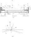
- Fig. 1 shows an optical fingerprint detection apparatus 100 according to an embodiment of the present disclosure.
- the optical fingerprint detection apparatus 100 comprises a light source 10 for emitting a light beam 11, a touch panel 20 and a detection unit 30.
- the touch panel 20 comprises a first surface 21 (an upper surface in Fig. 1 ) and at least one second surface 22 adjacent to the first surface 21.
- the first surface 21 is provided with at least one touch area 23 which is to be touched by a finger or a toe.
- the second surface 22 is configured for receiving the light beam 11 emitted from the light source 10 and angled with respect to the first surface 21 by an angle of less than 90 degrees so as to direct the light beam 11 transmitted through the second surface 22 into the touch panel 20 toward the touch area 23 of the first surface 21.
- the touch area 23 is arranged to totally reflect the light beam 11 toward a side (a lower side of the touch panel 20 in Fig. 1 ) of the touch panel 20 opposite to the first surface 21 when the touch area 23 is not touched by the finger or the toe.
- the detection unit 30 is located outside of the side of the touch panel 20 opposite to the first surface 21, i.e., outside of the lower side of the touch panel 20 (underneath the touch panel 20 in Fig. 1 ), and the detection unit 30 is configured for receiving the light beam 11 reflected by the touch area 23 and emitted from the touch panel 20 and detecting an intensity distribution of the received light beam 11.
- the detection unit 30 is, for example, a photoelectric sensor or any other detection device capable of detecting the optical signal strength.
- a refractive index of the touch panel 20 is greater than a refractive index of air, and the angle between the second surface 22 and the first surface 21 is arranged such that an incidence angle of the light beam 11 at the first surface 21 satisfies a total reflection condition when the first surface 21 is in contact with the air, and does not satisfy the total reflection condition when the first surface 21 is in direct contact with human skin.
- the refractive index of the touch panel 20 is typically, for example, less than the refractive index of the human skin, but this is not necessary, for example, the refractive index of the touch panel 20 is alternatively greater than or equal to the refractive index of the human skin as long as the total reflection condition is not satisfied when the first surface 21 comes into direct contact with the human skin.
- the human fingerprint consists of uneven texture structures having a certain pattern. Therefore, the fingerprint identification refers to reproduction of the uneven texture structures of the fingerprint.
- the raised portion of the fingerprint will be referred to as “ridge” and the recessed portion will be referred to as “valley”.
- Fig. 2 shows a schematic diagram of detecting finger fingerprint using the optical fingerprint detection apparatus according to the embodiment of the present disclosure.
- the "ridge" 81 in the fingerprint will be made in close contact with the touch area 23 and the “valley” 82 in the fingerprint will be kept away from the touch area 23 with a certain gap when the finger 80 presses against the touch area 23 of the first surface 21 of the touch panel 20.
- two kinds of interfaces are formed on the touch area 23.
- a region of the touch area 23 that is in contact with the "ridge” 81 in the fingerprint forms an interface between the finger 80 and the touch panel 20, and a region (including the region corresponding to the "valley” 82 in the fingerprint) of the touch area 23 that is not in contact with the "ridge” 81 in the fingerprint forms an interface between the touch panel 20 and a surrounding ambient media (typically air, but not limited thereto).
- a surrounding ambient media typically air, but not limited thereto.
- the light beam 11 remains totally reflected at the interface between the touch panel 20 and the surrounding ambient medium, while at the interface between the finger 80 and the touch panel 20, the total reflection condition is not satisified due to the relatively large refractive index of the finger 80 (generally about 1.55), in this case, a portion of the light beam cannot be reflected back into the interior of the touch panel 20 (for example, it is refracted into the finger skin (see the light ray C 1 in Fig. 2 ) and absorbed by the finger skin), thereby attenuating reflection strength of the light beam 11.
- an alternately bright and dark pattern will appear in the light beam 11 and has a dark region corresponding to the "ridge” 81 in the fingerprint and a bright region corresponding to the "valley” 82 in the fingerprint.
- the pattern is for example obtained through the detection of the light intensity distribution of the received light beam using the detection unit 30.
- the pattern can reflect the texture distribution characteristics of the fingerprint. By means of this pattern, it facilitates realizing the fingerprint identification.
- the angle between the first surface 21 and the second surface 22 needs to satisfy certain conditions, which are for example derived from geometrical optics principles.
- ⁇ is an angle between the first surface 21 and the second surface 22
- ⁇ ' is a refraction angle of the light beam 11 at the second surface 22
- ⁇ 1 is an incidence angle of the light beam 11 at the touch area 23
- w is a width of the touch area 23
- h is a thickness of the touch panel 20
- n is a medium refraction index of the touch panel 20.
- ⁇ c is a total reflection critical angle of the first surface 21 at the interface between the touch panel 20 and the surrounding ambient medium, the total reflection critical angle being determined by the refractive index of the touch panel 20 and the refractive index of the surrounding ambient medium.
- the refraction angle ⁇ ' of the light beam 11 at the second surface 22 is determined by the incidence angle of the light beam 11 at the second surface 22, the refractive index of the touch panel 20 and the refractive index of the surrounding ambient medium.
- the angle ⁇ between the second surface and the first surface is arranged such that the incidence angle ⁇ 1 of the light beam at the first surface is greater than or equal to the total reflection critical angle ⁇ c when the first surface is in contact with the air, and less than the total reflection critical angle ⁇ c when the first surface is in direct contact with the human skin.
- the range of the angle ⁇ between the first surface 21 and the second surface 22 depends on the refractive index of the touch panel 20, the refractive index of the surrounding ambient medium and the incidence angle of the light beam 11 at the second surface 22.
- the angle ⁇ between the first surface 21 and the second surface 22 may be for example determined according to the above equation (4).
- the range of values of w and h may be for example determined according to the relationship between the width w of the touch area 23 and the thickness h of the touch panel 20 in the above equation (3).
- the incident angle of the light beam 11 at the second surface 22 is, for example, 90°- ⁇ , i.e., the light beam 11 is incident onto the second surface 22 in a horizontal direction, as shown in Fig. 1 .
- the range of the angle ⁇ between the first surface 21 and the second surface 22 is maximized. This is beneficial for design and processing of the touch panel 20.
- the optical fingerprint detection apparatus 100 further comprises a frame 70 disposed around the second surface 22 of the touch panel 20.
- the frame 70 is for example used to hold and fix the touch panel 20.
- the light source 10 is for example arranged on an inner wall of the frame 70. Such an arrangement of the light source 10 facilitates the assembly of the optical fingerprint detection apparatus 100.
- the optical fingerprint detection apparatus 100 for example further comprises a display assembly 40 located between the touch panel 20 and the detection unit 30.
- the detection unit 30 is for example arranged to receive the light beam 11 emitted from the touch panel 20 and transmitted through the display assembly 40.
- the display assembly 40 comprises for example, a polarizer 41, a color filter 42 and a liquid crystal layer 43 in this order.
- the display assembly 40 is for example configured to display the location of the touch area 23, or for example configured to prompt the finger (or toe) when the touch area 23 is effective to be pressed by displaying information. This also facilitates the operation of the optical fingerprint identification.
- the optical fingerprint detection apparatus 100 further comprises a thin film transistor substrate 50, wherein the detection unit 30 is disposed between the liquid crystal layer 43 and the thin film transistor substrate 50.
- the detection unit 30 may be for example integrated with the display assembly 40 and the thin film transistor substrate 50 during fabrication, so as to simplify the process and achieve a compact structure.
- the liquid crystal display assembly is taken as an example to describe the present disclosure in the above examples, it should be understood that the present disclosure is not limited thereto.
- other types of display assemblies such as organic light emitting diode display assemblies
- the display assembly 40 is adhered on the side (the lower surface of the touch panel 20 in Fig. 1 ) of the touch panel 20 opposite to the first surface 21 via an adhesive layer 44, and the adhesive layer 44 is located between the touch panel 20 and the display assembly 40.
- the adhesive layer 44 for example, an OCA optical adhesive
- the adhesive layer 44 has a refractive index substantially equal to that of the touch panel 20, for example, the difference between the refractive index of the adhesive layer 44 and the refractive index of the touch panel 20 is within 1% of the refractive index of the adhesive layer 44 or the refractive index of the touch panel 20.
- the optical fingerprint detection apparatus 100 for example further comprises a light shielding portion 60 formed on a surface (the lower surface of the touch panel 20 in Fig. 1 ) of the touch panel 20 opposite to the first surface 21 and disposed around the display assembly 40 to form a non-display area.
- the light shielding portion 60 is configured to form a non-display area, which is for example used to form a trim, a keypad area, and the like.
- the light shielding portion 60 is for example formed of an ink coating.
- the detection unit 30 for example comprises a first detection portion 31 provided in a display area of the display assembly 40 and a second detection portion 32 provided in the non-display area of the display assembly 40.
- the first detection portion 31 is configured to receive a portion of the light beam 11 transmitted through a side 45 (the lower side of the display assembly 40 in Figs. 1 and 3 ) of the display assembly 40 facing away from the touch panel
- the second detection portion 32 is configured to receive a portion of the light beam 11 transmitted through a periphery 46 of the display assembly 40.
- the detection portions of the detection unit 40 are arranged within the display area and the non-display area of the display assembly 40, respectively, in this way, it increases the area of detection unit 30 receiving the optical signal, thereby increasing the area of the touch panel 23.
- the touch area 23 for example at least partially occupies a region on the first surface 21 corresponding to the light shielding portion 60, which further increases the area of the touch panel 23.
- L is an entire length of the first surface 21;
- L 1 is a width of the non-display area;
- L 2 is a distance from the right edge of the touch area 23 to the left edge of the right non-display area;
- ⁇ is an refraction angle of the light beam 11 at the periphery 46 of the display assembly 40;
- d is a thickness from the first surface 21 of the touch panel 23 to the detection unit 30 (or to the lower surface of the liquid crystal layer 43);
- d1 is a thickness from a position, at which the outermost edge of the light beam 11 exits from the periphery 46 of the display assembly 40,to the first surface 21 of the touch panel 23;
- d2 is a thickness from a position, at which the outermost edge of the light beam 11 exits from the periphery 46 of the display assembly 40, to the detection unit 30 (or to the lower surface of the liquid crystal layer 43);
- s is a width of a fingerprint detection area provided in the non-display area.
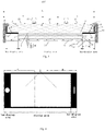
- Fig. 3 is a schematic cross-sectional view of an optical fingerprint detection apparatus 100' according to another embodiment of the present disclosure.
- two light sources 10 for emitting respective light beams 11 are provided.
- the first surface 21 of the touch panel 20 is provided with two touch areas 23 spaced apart from each other, and accordingly, the touch panel 20 is provided with two second surfaces 22 opposite to each other.
- Each of the second surfaces 22 receives the light beam 11 emitted from the corresponding light source 10 and directs it to the corresponding touch area 23, respectively.
- the total area of the touch area 23 on the first surface 21 is maximized.
- the operation principle thereof is the same as that of the foregoing embodiment.
- each of the second surfaces 22 is configured to be angled by an angle of less than 90 degrees with respect to the first surface 21 and to satisfy the total reflection requirement on the corresponding touch area 23.
- each of the touch areas 23 is for example correspondingly provided with a light shielding portion 60, a non-display area and the like.
- the remaining structures are substantially the same as those of the foregoing embodiment, and the detailed description thereof will not be repeated.
- angles between the second surfaces 22 and the first surface 21 are for example the same as or different from each other, so as to accommodate different design needs.
- Fig. 4 is a top view of the optical fingerprint detection apparatus 100' shown in Fig. 3 .
- the optical fingerprint detection apparatus having one or two touch regions is taken as an example to describe the present disclosure in the above embodiments, it should be understood that the present disclosure is not limited thereto.
- the first surface 21 of the optical fingerprint detection apparatus according to the embodiment of the present disclosure may for example have three, four, or more touch areas.
- Fig. 5 is a schematic top view of an optical fingerprint detection device 100" according to a further embodiment of the present disclosure.
- This embodiment differs from the embodiment shown in Fig. 3 only in that the light source 10 is arranged on the second surface 22.
- the light source 10 is arranged on the second surface 22, thereby for example reducing the light energy loss by directly directing the light beam 11 into the touch panel 20.
- such an arrangement also facilitates the incidence of the light beam 11 perpendicular to the second surface 22 to increase the range of the angle between the first surface 21 and the second surface 22.
- the light source 10 is for example affixed to the second surface 22, and the light source 10 is for example a flexible light source.
- n is a medium refractive index of the touch panel 20
- n' is a refractive index of the skin of the finger 80
- ⁇ is a reflectance of the light beam 11 at the interface between the finger 80 and the touch panel 20
- ⁇ 1 is an incidence angle of the light beam 11 on the touch area
- ⁇ 2 is a refraction angle of the light beam 11 at the interface between the finger 80 and the touch panel 20.
- an application of the optical fingerprint detection apparatus in a mobile phone with a 5 inches display screen is taken as an example, providing that a length of the display area is 110mm, a thickness h of the touch panel 20 is 0.55mm, a thickness of the adhesive layer 44 is 0.1mm, a thickness of the polarizer 41 is 0.1mm, a thickness of the color filter 42 is 0.2mm, and a thickness of the liquid crystal layer 43 is 0.003mm, then the thickness d from the first surface 21 of the touch panel 23 to the lower surface of the liquid crystal layer 43 is 0.953mm, the width of the non-display area is equal to 15mm, the entire length L1 of the touch panel 20 is equal to 110+2 ⁇ s, which is equal to 140mm, and the medium refractive index n of the touch panel 20 is equal to 1.5163.
- the width w of the touch area 23 is equal to 53.81mm
- the width s of the fingerprint detection area provided in the non-display area is equal to 14.53mm
- the width of the touch area 23 is for example 53.81mm.
- the touch panel 20 is made of glass, it can be for example derived from the equations (12)-(13) that the reflectance ⁇ of the light beam 11 at the interface between the finger 80 and the touch panel 20 (at the "ridge" 81 of the fingerprint) is equal to 82.1%.
- the reflectance ⁇ of the light beam 11 at the interface between the finger 80 and the touch panel 20 is lower, the difference between the light intensity signals corresponding to the "valley” 82 and the "ridge” 81 of the fingerprint is greater, and the detected fingerprint image is more clear.
- Table 1 ⁇ 2w ⁇ 88.28° 2 ⁇ 53.81mm 82.1% 87° 2 ⁇ 30.86mm 70.9% 85° 2 ⁇ 18.53mm 56.4%
- Table 1 shows exemplary results of the width w (2w refers to the case of two touch areas) of the touch area 23 and the change of the reflectance ⁇ with respect to ⁇ in the embodiment shown in Fig. 3 . It can be seen from Table 1 that the reflectance ⁇ decreases as ⁇ becomes smaller, but the width w of the touch area 23 also becomes small.
- an appropriate value of ⁇ is chosen, for example, according to the actual requirements, such as the desired area of the touch area 23 and the detection performance of the detection unit 30 and so on.
- the angle between the first surface 21 and the second surface 22 may be selected to be less than 88 degrees, less than 87 degrees, or less than 85 degrees, etc.
- the touch panel 20 is for example made of at least one of a variety of completely transparent or partially transparent materials, such as glass, quartz, plastic, resin and the like.
- the total area of the touch area 23 for example accounts for 10%, 30%, 50%, or 70% or more of the area of the first surface 21. This facilitates achieving a large area fingerprint identification area on the display screen.
- the light source 10 is for example a surface light source. This for example allows the light beam 11 emitted from the light source 10 to be a uniform parallel light beam, thereby improving the optical detection effect. But this is not necessary, for example, the light source 10 may also use other types of light sources, such as a LED spot light source.
- the fingerprint "valley” and “ridge” signals obtained by the optical fingerprint detection apparatus may for example be compared and identified by any one of fingerprint identification algorithms in the prior arts.
- the optical fingerprint detection apparatus is not only configured to detect a fingerprint of a finger, but also configured to alternatively detect a skin texture structure of other parts of the human body, such as a toe fingerprint, a dermatoglyph and the like.
- the embodiments of the present disclosure also provide a display device comprising the optical fingerprint detection apparatus 100, 100', 100" according to any one of the above-described embodiments.
- the display device can have an accurate optical fingerprint detection function.
Landscapes
- Engineering & Computer Science (AREA)
- Theoretical Computer Science (AREA)
- Human Computer Interaction (AREA)
- Physics & Mathematics (AREA)
- General Physics & Mathematics (AREA)
- General Engineering & Computer Science (AREA)
- Multimedia (AREA)
- Image Input (AREA)
- Measurement Of The Respiration, Hearing Ability, Form, And Blood Characteristics Of Living Organisms (AREA)
Claims (13)
- Appareil de détection d'empreintes digitales optiques (100,100', 100"), comprenant :une source de lumière (10) pour émettre un faisceau lumineux (11) ;un panneau tactile transparent (20) comprenant une première surface (21) et au moins une seconde surface (22) adjacente à la première surface (21), la première surface (21) étant pourvue d'au moins une zone tactile (23) qui doit être touchée par un doigt ou un orteil, la seconde surface (22) étant conçue pour recevoir le faisceau lumineux (11) émis par la source de lumière (10) et étant en angle par rapport à la première surface (21) d'un angle de moins de 90° de manière à diriger le faisceau lumineux (11) transmis à travers la seconde surface (22) dans le panneau tactile (20) vers la zone tactile (23) de la première surface (21), et la zone tactile (23) étant conçue pour réfléchir totalement le faisceau lumineux (11) vers un côté du panneau tactile (20) opposé à la première surface (21) lorsque la zone tactile (23) n'est pas touchée par le doigt ou l'orteil ; etune unité de détection (30) située à l'extérieur du côté du panneau tactile (20) opposé à la première surface (21) et conçu pour recevoir le faisceau lumineux (11) réfléchi par la zone tactile (23) et émis par le panneau tactile (20) et détectant une répartition d'intensité du faisceau lumineux reçu (11),un indice de réfraction du panneau tactile (20) étant supérieur à un indice de réfraction de l'air, et l'angle entre la seconde surface (22) et la première surface (21) étant conçu pour qu'un angle d'incidence du faisceau lumineux (11) à la première surface (21) satisfasse à une condition de réflexion total lorsque la première surface (21) est en contact avec l'air, et ne satisfasse pas à la condition de réflexion total lorsque la première surface (21) est en contact direct avec la peau humaine,caractérisé en ce quel'appareil de détection d'empreintes digitales optiques (100,100', 100") comprend en outre un cadre (70) disposé autour du panneau tactile (20), la source de lumière (10) correspondant à la seconde surface (22) étant disposée sur une paroi intérieure du cadre (70) ;l'appareil de détection d'empreintes digitales optiques (100,100', 100") comprend en outre un ensemble d'affichage(40) situé entre le panneau tactile (20) et l'unité de détection (30) ; etl'ensemble d'affichage et l'unité de détection se situent dans le cadre (70), et l'unité de détection est conçue pour recevoir le faisceau lumineux émis par le panneau tactile et transmis à travers l'ensemble d'affichage.
- Appareil de détection d'empreintes digitales optiques (100,100', 100") selon la revendication 1, dans lequel le faisceau lumineux (11) est émis perpendiculairement à la seconde surface (22).
- Appareil de détection d'empreintes digitales optiques (100,100', 100") selon la revendication 1, dans lequel l'ensemble d'affichage (40) comprend un polariseur (41), un filtre en couleurs (42), et une couche de cristaux liquides (43) dans cet ordre.
- Appareil de détection d'empreintes digitales optiques (100,100', 100") selon la revendication 3, comprenant en outre un substrat à transistor à film mince (50), l'unité de détection (30) étant disposée entre la couche de cristaux liquides (43) et le substrat à transistor à film mince (50).
- Appareil de détection d'empreintes digitales optiques (100,100', 100") selon la revendication 1, dans lequel l'ensemble d'affichage (40) est collé sur le côté du panneau tactile (20) opposé à la première surface (21) par une couche adhésive (44), et la couche adhésive (44) se trouve entre le panneau tactile (20) et l'ensemble d'affichage (40) et a un indice de réfraction substantiellement égal à celui du panneau tactile (20).
- Appareil de détection d'empreintes digitales optiques (100,100', 100") selon la revendication 1, comprenant en outre une section faisant écran à la lumière (60) formée sur une surface du panneau tactile (20) opposée à la première surface (21) et disposée autour de l'ensemble d'affichage (40) pour former une zone sans affichage.
- Appareil de détection d'empreintes digitales optiques (100,100', 100") selon la revendication 6, dans lequel l'unité de détection (30) comprend une première section de détection (31) prévue dans une zone d'affichage de l'ensemble d'affichage (40) et une seconde section de détection (32) prévue dans la zone sans affichage de l'ensemble d'affichage (40), la première section de détection (31) étant conçue pour recevoir une partie du faisceau lumineux (11) émise depuis un côté de l'ensemble d'affichage (40) détourné du panneau tactile (20), et la seconde section de détection (32) étant configurée pour recevoir une partie du faisceau lumineux (11) émise depuis une périphérie de l'ensemble d'affichage (40).
- Appareil de détection d'empreintes digitales optiques (100,100', 100") selon la revendication 6, dans lequel la zone active (23) occupe au moins partiellement une zone de la première surface (21) correspondant à la section faisant écran à la lumière (60).
- Appareil de détection d'empreintes digitales optiques (100', 100") selon l'une quelconque des revendications 1 à 8, l'appareil de détection d'empreintes digitales optiques (100, 100") comprenant deux sources de lumière (10) dont chacune émet un faisceau lumineux (11), la première surface (21) étant pourvue de deux zones tactiles (23) espacées l'une de l'autre, et le panneau tactile (20) étant pourvu de deux secondes surfaces (22) tournées l'une vers l'autre, les deux secondes surfaces (22) recevant respectivement les faisceaux lumineux (11) émis par les deux sources de lumière (10) et dirigeant respectivement les faisceaux lumineux (11) vers les deux zones tactiles (23).
- Appareil de détection d'empreintes digitales optiques (100,100', 100") selon l'une quelconque des revendications 1 à 8, dans lequel le panneau tactile (20) est composé d'au moins un matériau parmi le verre, le quartz, le plastique et la résine, ou la source lumineuse (10) est une source lumineuse de surface.
- Appareil de détection d'empreintes digitales optiques (100,100', 100") selon l'une quelconque des revendications 1 à 8, dans lequel une zone de la zone tactile (23) occupe 70 % ou plus d'une zone de la première surface (21).
- Appareil de détection d'empreintes digitales optiques (100,100', 100") selon la revendication 1, dans lequel l'angle d'incidence du faisceau lumineux (11) sur la première surface (21) a un angle critique de réflexion total (θc) où la réflexion du faisceau lumineux (11) sur la première surface (21) change entre la condition de réflexion total et une condition de réflexion non totale, l'angle critique de réflexion total (θc) étant déterminé par l'indice de réfraction du panneau tactile (20) et un indice de réfraction d'un fluide ambiant environnant en contact direct avec la première surface (21).
- Appareil de détection d'empreintes digitales optiques (100,100', 100") selon la revendication 12, dans lequel l'angle entre la seconde surface (22) et la première surface (21) est conçu de manière à ce que l'angle d'incidence du faisceau lumineux (11) à la première surface (21) soit supérieur ou égale à l'angle critique de réflexion total (θc) lorsque la première surface (21) est en contact avec l'air, et inférieur à l'angle critique de réflexion total (θc) lorsque la première surface (21) est en contact direct avec la peau humaine.
Applications Claiming Priority (2)
| Application Number | Priority Date | Filing Date | Title |
|---|---|---|---|
| CN201510661890.5A CN105184282B (zh) | 2015-10-14 | 2015-10-14 | 光学指纹检测装置及显示设备 |
| PCT/CN2016/087827 WO2017063384A1 (fr) | 2015-10-14 | 2016-06-30 | Dispositif de détection d'empreintes digitales optique et appareil d'affichage |
Publications (3)
| Publication Number | Publication Date |
|---|---|
| EP3196802A1 EP3196802A1 (fr) | 2017-07-26 |
| EP3196802A4 EP3196802A4 (fr) | 2018-05-30 |
| EP3196802B1 true EP3196802B1 (fr) | 2020-10-28 |
Family
ID=54906348
Family Applications (1)
| Application Number | Title | Priority Date | Filing Date |
|---|---|---|---|
| EP16825694.9A Not-in-force EP3196802B1 (fr) | 2015-10-14 | 2016-06-30 | Appareil de détection d'empreintes digitales optique |
Country Status (4)
| Country | Link |
|---|---|
| US (1) | US9996724B2 (fr) |
| EP (1) | EP3196802B1 (fr) |
| CN (1) | CN105184282B (fr) |
| WO (1) | WO2017063384A1 (fr) |
Families Citing this family (82)
| Publication number | Priority date | Publication date | Assignee | Title |
|---|---|---|---|---|
| US10732771B2 (en) | 2014-11-12 | 2020-08-04 | Shenzhen GOODIX Technology Co., Ltd. | Fingerprint sensors having in-pixel optical sensors |
| US10437974B2 (en) | 2015-06-18 | 2019-10-08 | Shenzhen GOODIX Technology Co., Ltd. | Optical sensing performance of under-screen optical sensor module for on-screen fingerprint sensing |
| KR101928319B1 (ko) | 2015-06-18 | 2018-12-12 | 선전 구딕스 테크놀로지 컴퍼니, 리미티드 | 광 감지 능력을 가지는 다기능 지문 센서 |
| CN107004130B (zh) * | 2015-06-18 | 2020-08-28 | 深圳市汇顶科技股份有限公司 | 用于屏幕上指纹感应的屏幕下光学传感器模块 |
| US10410037B2 (en) | 2015-06-18 | 2019-09-10 | Shenzhen GOODIX Technology Co., Ltd. | Under-screen optical sensor module for on-screen fingerprint sensing implementing imaging lens, extra illumination or optical collimator array |
| US10410033B2 (en) | 2015-06-18 | 2019-09-10 | Shenzhen GOODIX Technology Co., Ltd. | Under-LCD screen optical sensor module for on-screen fingerprint sensing |
| CN105184248B (zh) * | 2015-08-28 | 2019-03-12 | 京东方科技集团股份有限公司 | 一种指纹识别装置及指纹识别系统 |
| CN105184282B (zh) | 2015-10-14 | 2019-04-23 | 京东方科技集团股份有限公司 | 光学指纹检测装置及显示设备 |
| US10438046B2 (en) | 2015-11-02 | 2019-10-08 | Shenzhen GOODIX Technology Co., Ltd. | Multifunction fingerprint sensor having optical sensing against fingerprint spoofing |
| CN106951816A (zh) * | 2016-01-07 | 2017-07-14 | 上海箩箕技术有限公司 | 光学指纹传感器模组 |
| EP3254235B1 (fr) * | 2016-01-31 | 2023-07-12 | Shenzhen Goodix Technology Co., Ltd. | Module de capteur optique de sous-écran permettant la détection d'empreintes digitales sur écran |
| CN105808021B (zh) * | 2016-03-09 | 2021-01-22 | 京东方科技集团股份有限公司 | 光感式触控面板、显示装置和触摸定位方法 |
| CN107341433B (zh) * | 2016-04-28 | 2023-12-26 | 渭南印象认知技术有限公司 | 隐藏式指纹采集器 |
| KR102040651B1 (ko) | 2016-04-29 | 2019-11-06 | 엘지디스플레이 주식회사 | 광학식 이미지 인식 센서 내장형 평판 표시장치 |
| DE102016108634A1 (de) * | 2016-05-10 | 2017-11-16 | Preh Gmbh | Eingabegerät mit Berühr- beziehungsweise Betätigungsverifizierung |
| CN106022276B (zh) * | 2016-05-25 | 2019-06-07 | 京东方科技集团股份有限公司 | 指纹识别器件及其制作方法、显示器件、显示装置 |
| CN105844270B (zh) * | 2016-06-15 | 2019-05-17 | 京东方科技集团股份有限公司 | 指纹识别装置及其制作方法、液晶显示器 |
| CN106095211B (zh) | 2016-06-30 | 2019-06-18 | 京东方科技集团股份有限公司 | 显示面板及其制备方法、显示装置 |
| US20180032778A1 (en) * | 2016-07-29 | 2018-02-01 | Microsoft Technology Licensing, Llc | Display with a touch sensor |
| CN106228144B (zh) * | 2016-08-02 | 2023-10-13 | 京东方科技集团股份有限公司 | 一种指纹识别显示装置 |
| CN106970495A (zh) * | 2016-09-14 | 2017-07-21 | 北京小米移动软件有限公司 | 阵列基板及其制作方法、显示面板、显示装置和电子设备 |
| KR102693504B1 (ko) | 2016-09-26 | 2024-08-12 | 삼성디스플레이 주식회사 | 표시장치 및 그의 구동방법 |
| CN106529487A (zh) * | 2016-11-18 | 2017-03-22 | 上海箩箕技术有限公司 | 光学指纹传感器模组 |
| KR102570180B1 (ko) * | 2016-11-28 | 2023-08-25 | 엘지디스플레이 주식회사 | 지문 센서 일체형 전계 발광 표시장치 |
| KR102136553B1 (ko) | 2016-11-30 | 2020-07-22 | 주식회사 엘지화학 | 디지털 디바이스의 제어 방법 |
| EP3334130B1 (fr) | 2016-12-08 | 2021-06-09 | LG Display Co., Ltd. | Écran plat intégrant un capteur d'imagerie optique |
| KR102440209B1 (ko) * | 2016-12-08 | 2022-09-05 | 엘지디스플레이 주식회사 | 광학식 이미지 인식 센서 내장형 평판 표시장치 |
| CN108229241A (zh) | 2016-12-09 | 2018-06-29 | 上海箩箕技术有限公司 | 显示模组及其使用方法 |
| CN108227973A (zh) * | 2016-12-09 | 2018-06-29 | 上海箩箕技术有限公司 | 显示模组及其使用方法 |
| CN108614982A (zh) * | 2016-12-09 | 2018-10-02 | 上海箩箕技术有限公司 | 显示模组及其使用方法 |
| CN108614983A (zh) * | 2016-12-09 | 2018-10-02 | 上海箩箕技术有限公司 | 显示模组及其使用方法 |
| CN108399351A (zh) * | 2017-02-04 | 2018-08-14 | 上海箩箕技术有限公司 | 指纹成像模组和电子设备 |
| KR102747024B1 (ko) * | 2017-02-07 | 2024-12-30 | 삼성디스플레이 주식회사 | 표시 장치 |
| US10614283B2 (en) | 2017-03-07 | 2020-04-07 | Shenzhen GOODIX Technology Co., Ltd. | Devices with peripheral task bar display zone and under-LCD screen optical sensor module for on-screen fingerprint sensing |
| CN108629256A (zh) * | 2017-03-24 | 2018-10-09 | 上海箩箕技术有限公司 | 指纹成像模组和电子设备 |
| CN106940488B (zh) * | 2017-04-27 | 2019-07-12 | 上海天马微电子有限公司 | 显示面板及显示装置 |
| KR102418802B1 (ko) | 2017-05-02 | 2022-07-11 | 엘지디스플레이 주식회사 | 표시장치 |
| CN107145868A (zh) * | 2017-05-09 | 2017-09-08 | 上海箩箕技术有限公司 | 显示模组 |
| WO2018205124A1 (fr) * | 2017-05-09 | 2018-11-15 | 上海箩箕技术有限公司 | Module d'affichage |
| CN107145869A (zh) * | 2017-05-09 | 2017-09-08 | 上海箩箕技术有限公司 | 显示模组 |
| WO2018205121A1 (fr) * | 2017-05-09 | 2018-11-15 | 上海箩箕技术有限公司 | Module d'affichage |
| CN107273808A (zh) * | 2017-05-19 | 2017-10-20 | 上海箩箕技术有限公司 | 显示模组 |
| CN107247925A (zh) * | 2017-05-19 | 2017-10-13 | 上海箩箕技术有限公司 | 显示模组 |
| CN107480584B (zh) * | 2017-07-05 | 2021-11-26 | 上海交通大学 | 扫描式指纹识别与触控一体屏 |
| KR102389197B1 (ko) * | 2017-08-16 | 2022-04-21 | 엘지디스플레이 주식회사 | 표시장치 |
| CN109426022A (zh) * | 2017-08-31 | 2019-03-05 | 上海箩箕技术有限公司 | 显示模组 |
| CN109426784A (zh) * | 2017-08-31 | 2019-03-05 | 上海箩箕技术有限公司 | 显示模组 |
| CN109426790A (zh) * | 2017-08-31 | 2019-03-05 | 上海箩箕技术有限公司 | 显示模组 |
| KR102460111B1 (ko) * | 2017-09-07 | 2022-10-28 | 엘지디스플레이 주식회사 | 광학식 이미지 인식 센서 내장형 평판 표시장치 |
| CN107644202B (zh) * | 2017-09-08 | 2021-01-08 | 维沃移动通信有限公司 | 一种光学指纹模组及移动终端 |
| KR102462246B1 (ko) | 2017-09-11 | 2022-11-02 | 엘지디스플레이 주식회사 | 표시장치와 이 표시장치를 포함한 모바일 정보 단말기 |
| CN107977627B (zh) * | 2017-11-30 | 2023-12-08 | 北京集创北方科技股份有限公司 | 纹路的光学检测装置、电子设备及纹路的光学检测方法 |
| KR102535177B1 (ko) | 2017-12-21 | 2023-05-23 | 엘지디스플레이 주식회사 | 지문 인식 장치와 이를 포함한 표시장치와 모바일 단말기 |
| CN108108718A (zh) * | 2018-01-05 | 2018-06-01 | 敦捷光电股份有限公司 | 屏内光学指纹辨识的薄膜晶体管面板 |
| CN108091680B (zh) * | 2018-01-05 | 2022-11-08 | 敦泰电子有限公司 | 屏内光学指纹辨识的发光二极管面板 |
| US10303921B1 (en) * | 2018-02-26 | 2019-05-28 | Shenzhen GOODIX Technology Co., Ltd. | On-LCD screen optical fingerprint sensing based on optical imaging with lens-pinhole module and other optical designs |
| CN108615005B (zh) * | 2018-04-20 | 2021-06-08 | Oppo广东移动通信有限公司 | 指纹识别组件、显示装置及电子装置 |
| CN108667963B (zh) | 2018-04-23 | 2019-04-16 | Oppo广东移动通信有限公司 | 电子设备 |
| CN108885697B (zh) | 2018-06-15 | 2021-11-05 | 深圳市汇顶科技股份有限公司 | 屏下生物特征识别装置和电子设备 |
| CN109299708B (zh) * | 2018-11-30 | 2024-05-14 | 上海箩箕技术有限公司 | 光学指纹传感器模组及其形成方法 |
| TWI715322B (zh) * | 2018-12-07 | 2021-01-01 | 鴻海精密工業股份有限公司 | 液晶顯示裝置 |
| CN109726650B (zh) * | 2018-12-17 | 2021-04-16 | Oppo广东移动通信有限公司 | 显示屏、电子设备及指纹处理方法 |
| CN110785771B (zh) * | 2019-01-22 | 2023-09-08 | 深圳市汇顶科技股份有限公司 | 屏下光学指纹识别系统、指纹识别显示装置及电子设备 |
| CN109637376B (zh) * | 2019-01-31 | 2022-02-18 | 厦门天马微电子有限公司 | 显示装置 |
| CN109886177B (zh) * | 2019-02-14 | 2021-08-24 | Oppo广东移动通信有限公司 | 显示屏模组、电子设备及指纹图像处理方法 |
| CN110008869B (zh) * | 2019-03-25 | 2021-04-30 | 厦门天马微电子有限公司 | 显示面板和显示装置 |
| WO2021016851A1 (fr) * | 2019-07-30 | 2021-02-04 | 深圳市汇顶科技股份有限公司 | Composant d'identification d'empreintes digitales, module d'affichage d'identification d'empreintes digitales optique et dispositif électronique |
| CN112307843B (zh) * | 2019-07-31 | 2025-02-07 | 深圳阜时科技有限公司 | 光学检测装置 |
| CN112307838B (zh) * | 2019-07-31 | 2024-11-15 | 深圳阜时科技有限公司 | 光学检测装置 |
| CN110503019A (zh) * | 2019-08-16 | 2019-11-26 | 深圳阜时科技有限公司 | 光学检测装置 |
| CN112307837A (zh) * | 2019-07-31 | 2021-02-02 | 深圳阜时科技有限公司 | 电子产品 |
| CN112307845B (zh) * | 2019-07-31 | 2024-07-19 | 深圳阜时科技有限公司 | 光学检测装置 |
| CN112307836B (zh) * | 2019-07-31 | 2024-12-24 | 深圳阜时科技有限公司 | 光学检测装置和电子产品 |
| CN112307844A (zh) * | 2019-07-31 | 2021-02-02 | 深圳阜时科技有限公司 | 光学检测装置 |
| CN112307835B (zh) * | 2019-07-31 | 2024-07-23 | 深圳阜时科技有限公司 | 光学检测装置 |
| CN111108509B (zh) * | 2019-08-08 | 2023-09-08 | 深圳市汇顶科技股份有限公司 | 指纹检测装置和电子设备 |
| CN110458124B (zh) * | 2019-08-16 | 2024-09-20 | 深圳阜时科技有限公司 | 光学检测装置 |
| CN110945525B (zh) * | 2019-10-31 | 2023-08-22 | 深圳市汇顶科技股份有限公司 | 用于指纹识别的方法、指纹识别装置和电子设备 |
| CN111339820B (zh) * | 2019-12-18 | 2024-07-23 | 深圳阜时科技有限公司 | 一种光学检测装置及电子设备 |
| CN111199190B (zh) * | 2019-12-19 | 2024-08-13 | 深圳阜时科技有限公司 | 光学检测装置 |
| CN119888802A (zh) | 2019-12-26 | 2025-04-25 | 群创光电股份有限公司 | 电子装置 |
| CN111259847B (zh) | 2020-01-21 | 2024-01-26 | 维沃移动通信有限公司 | 一种电子设备 |
Family Cites Families (13)
| Publication number | Priority date | Publication date | Assignee | Title |
|---|---|---|---|---|
| JP2005228191A (ja) * | 2004-02-16 | 2005-08-25 | Nippon Raiton Kk | 指紋画像入力装置 |
| CN101169824B (zh) * | 2006-10-25 | 2011-04-20 | 原相科技股份有限公司 | 指纹辨识装置及方法 |
| CN101276406B (zh) * | 2007-03-29 | 2011-05-04 | 鸿富锦精密工业(深圳)有限公司 | 指纹识别装置及便携式电子装置 |
| CN101814125A (zh) * | 2009-02-25 | 2010-08-25 | 金佶科技有限公司 | 光学指纹识别系统 |
| US9880653B2 (en) * | 2012-04-30 | 2018-01-30 | Corning Incorporated | Pressure-sensing touch system utilizing total-internal reflection |
| WO2014018121A1 (fr) * | 2012-07-26 | 2014-01-30 | Changello Enterprise Llc | Estimation de force assistée par empreinte digitale |
| TW201409324A (zh) * | 2012-08-21 | 2014-03-01 | Wintek Corp | 觸控顯示面板及其光學式觸控面板 |
| WO2015005959A1 (fr) * | 2013-04-01 | 2015-01-15 | Patrick Baudisch | Écran tactile apte à reconnaissance d'empreinte digitale |
| US9880328B2 (en) * | 2013-12-12 | 2018-01-30 | Corning Incorporated | Transparent diffusers for lightguides and luminaires |
| CN104751121B (zh) * | 2015-03-05 | 2019-04-05 | 上海交通大学 | 基于光栅结构的光波导式指纹识别系统 |
| CN105184248B (zh) * | 2015-08-28 | 2019-03-12 | 京东方科技集团股份有限公司 | 一种指纹识别装置及指纹识别系统 |
| CN105184282B (zh) | 2015-10-14 | 2019-04-23 | 京东方科技集团股份有限公司 | 光学指纹检测装置及显示设备 |
| CN205068439U (zh) * | 2015-10-14 | 2016-03-02 | 京东方科技集团股份有限公司 | 光学指纹检测装置及显示设备 |
-
2015
- 2015-10-14 CN CN201510661890.5A patent/CN105184282B/zh not_active Expired - Fee Related
-
2016
- 2016-06-30 US US15/328,192 patent/US9996724B2/en not_active Expired - Fee Related
- 2016-06-30 EP EP16825694.9A patent/EP3196802B1/fr not_active Not-in-force
- 2016-06-30 WO PCT/CN2016/087827 patent/WO2017063384A1/fr not_active Ceased
Non-Patent Citations (1)
| Title |
|---|
| None * |
Also Published As
| Publication number | Publication date |
|---|---|
| CN105184282A (zh) | 2015-12-23 |
| EP3196802A4 (fr) | 2018-05-30 |
| EP3196802A1 (fr) | 2017-07-26 |
| US9996724B2 (en) | 2018-06-12 |
| US20170270340A1 (en) | 2017-09-21 |
| CN105184282B (zh) | 2019-04-23 |
| WO2017063384A1 (fr) | 2017-04-20 |
Similar Documents
| Publication | Publication Date | Title |
|---|---|---|
| US9996724B2 (en) | Optical fingerprint detection apparatus and display device | |
| US9811710B2 (en) | Fingerprint identifying device and fingerprint identifying system | |
| US10628656B2 (en) | Image capture apparatus | |
| CN205068439U (zh) | 光学指纹检测装置及显示设备 | |
| KR102418802B1 (ko) | 표시장치 | |
| US20100053118A1 (en) | Display module | |
| EP3159825A1 (fr) | Appareil d'acquisition d'images, dispositif terminal, dispositif terminal à cristaux liquides et procédé d'acquisition d'images | |
| US10735634B2 (en) | Image capture apparatus | |
| WO2018171178A1 (fr) | Dispositif d'identification d'empreintes digitales, procédé de commande, panneau d'affichage tactile et dispositif d'affichage tactile | |
| KR20170124160A (ko) | 광학식 이미지 인식 센서 내장형 평판 표시장치 | |
| US10956702B2 (en) | Apparatus for recognizing a fingerprint, and display device | |
| US20100259492A1 (en) | Touch panel display with infrared light source | |
| KR20180062202A (ko) | 박막 평판형 광학 이미지 센서 및 광학 이미지 센서 내장형 평판 표시장치 | |
| KR20180068040A (ko) | 광학식 이미지 인식 센서 내장형 평판 표시장치 | |
| CN111414830B (zh) | 指纹检测装置、触控面板和电子设备 | |
| CN108399392A (zh) | 指纹识别结构和显示装置 | |
| US20210064836A1 (en) | Electronic device | |
| CN108540605A (zh) | 指纹识别组件、显示装置及电子装置 | |
| CN108803781B (zh) | 具有光学成像传感器的平板显示器 | |
| CN111767901B (zh) | 显示装置 | |
| US11100309B2 (en) | Fingerprint sensing device | |
| CN210109513U (zh) | 用于lcd屏内指纹识别的背光模组 | |
| CN210573091U (zh) | 纹路识别装置和显示设备 | |
| CN210109371U (zh) | 一种增亮膜 | |
| KR102440209B1 (ko) | 광학식 이미지 인식 센서 내장형 평판 표시장치 |
Legal Events
| Date | Code | Title | Description |
|---|---|---|---|
| STAA | Information on the status of an ep patent application or granted ep patent |
Free format text: STATUS: UNKNOWN |
|
| STAA | Information on the status of an ep patent application or granted ep patent |
Free format text: STATUS: THE INTERNATIONAL PUBLICATION HAS BEEN MADE |
|
| PUAI | Public reference made under article 153(3) epc to a published international application that has entered the european phase |
Free format text: ORIGINAL CODE: 0009012 |
|
| STAA | Information on the status of an ep patent application or granted ep patent |
Free format text: STATUS: REQUEST FOR EXAMINATION WAS MADE |
|
| 17P | Request for examination filed |
Effective date: 20170123 |
|
| AK | Designated contracting states |
Kind code of ref document: A1 Designated state(s): AL AT BE BG CH CY CZ DE DK EE ES FI FR GB GR HR HU IE IS IT LI LT LU LV MC MK MT NL NO PL PT RO RS SE SI SK SM TR |
|
| AX | Request for extension of the european patent |
Extension state: BA ME |
|
| A4 | Supplementary search report drawn up and despatched |
Effective date: 20180502 |
|
| RIC1 | Information provided on ipc code assigned before grant |
Ipc: G02F 1/1333 20060101ALN20180424BHEP Ipc: G06K 9/00 20060101AFI20180424BHEP Ipc: G02F 1/1335 20060101ALN20180424BHEP Ipc: G02F 1/1368 20060101ALN20180424BHEP Ipc: G06F 3/042 20060101ALN20180424BHEP |
|
| STAA | Information on the status of an ep patent application or granted ep patent |
Free format text: STATUS: EXAMINATION IS IN PROGRESS |
|
| 17Q | First examination report despatched |
Effective date: 20190102 |
|
| DAV | Request for validation of the european patent (deleted) | ||
| DAX | Request for extension of the european patent (deleted) | ||
| GRAP | Despatch of communication of intention to grant a patent |
Free format text: ORIGINAL CODE: EPIDOSNIGR1 |
|
| STAA | Information on the status of an ep patent application or granted ep patent |
Free format text: STATUS: GRANT OF PATENT IS INTENDED |
|
| RIC1 | Information provided on ipc code assigned before grant |
Ipc: G06K 9/00 20060101AFI20200506BHEP Ipc: G02F 1/1335 20060101ALN20200506BHEP Ipc: G06F 3/042 20060101ALN20200506BHEP Ipc: G02F 1/1333 20060101ALN20200506BHEP Ipc: G02F 1/1368 20060101ALN20200506BHEP |
|
| INTG | Intention to grant announced |
Effective date: 20200519 |
|
| GRAS | Grant fee paid |
Free format text: ORIGINAL CODE: EPIDOSNIGR3 |
|
| GRAA | (expected) grant |
Free format text: ORIGINAL CODE: 0009210 |
|
| STAA | Information on the status of an ep patent application or granted ep patent |
Free format text: STATUS: THE PATENT HAS BEEN GRANTED |
|
| AK | Designated contracting states |
Kind code of ref document: B1 Designated state(s): AL AT BE BG CH CY CZ DE DK EE ES FI FR GB GR HR HU IE IS IT LI LT LU LV MC MK MT NL NO PL PT RO RS SE SI SK SM TR |
|
| REG | Reference to a national code |
Ref country code: GB Ref legal event code: FG4D |
|
| REG | Reference to a national code |
Ref country code: CH Ref legal event code: EP |
|
| REG | Reference to a national code |
Ref country code: AT Ref legal event code: REF Ref document number: 1328947 Country of ref document: AT Kind code of ref document: T Effective date: 20201115 |
|
| REG | Reference to a national code |
Ref country code: DE Ref legal event code: R096 Ref document number: 602016046838 Country of ref document: DE |
|
| REG | Reference to a national code |
Ref country code: IE Ref legal event code: FG4D |
|
| REG | Reference to a national code |
Ref country code: AT Ref legal event code: MK05 Ref document number: 1328947 Country of ref document: AT Kind code of ref document: T Effective date: 20201028 |
|
| REG | Reference to a national code |
Ref country code: NL Ref legal event code: MP Effective date: 20201028 |
|
| PG25 | Lapsed in a contracting state [announced via postgrant information from national office to epo] |
Ref country code: GR Free format text: LAPSE BECAUSE OF FAILURE TO SUBMIT A TRANSLATION OF THE DESCRIPTION OR TO PAY THE FEE WITHIN THE PRESCRIBED TIME-LIMIT Effective date: 20210129 Ref country code: FI Free format text: LAPSE BECAUSE OF FAILURE TO SUBMIT A TRANSLATION OF THE DESCRIPTION OR TO PAY THE FEE WITHIN THE PRESCRIBED TIME-LIMIT Effective date: 20201028 Ref country code: NO Free format text: LAPSE BECAUSE OF FAILURE TO SUBMIT A TRANSLATION OF THE DESCRIPTION OR TO PAY THE FEE WITHIN THE PRESCRIBED TIME-LIMIT Effective date: 20210128 Ref country code: NL Free format text: LAPSE BECAUSE OF FAILURE TO SUBMIT A TRANSLATION OF THE DESCRIPTION OR TO PAY THE FEE WITHIN THE PRESCRIBED TIME-LIMIT Effective date: 20201028 Ref country code: PT Free format text: LAPSE BECAUSE OF FAILURE TO SUBMIT A TRANSLATION OF THE DESCRIPTION OR TO PAY THE FEE WITHIN THE PRESCRIBED TIME-LIMIT Effective date: 20210301 Ref country code: RS Free format text: LAPSE BECAUSE OF FAILURE TO SUBMIT A TRANSLATION OF THE DESCRIPTION OR TO PAY THE FEE WITHIN THE PRESCRIBED TIME-LIMIT Effective date: 20201028 |
|
| REG | Reference to a national code |
Ref country code: LT Ref legal event code: MG4D |
|
| PG25 | Lapsed in a contracting state [announced via postgrant information from national office to epo] |
Ref country code: ES Free format text: LAPSE BECAUSE OF FAILURE TO SUBMIT A TRANSLATION OF THE DESCRIPTION OR TO PAY THE FEE WITHIN THE PRESCRIBED TIME-LIMIT Effective date: 20201028 Ref country code: AT Free format text: LAPSE BECAUSE OF FAILURE TO SUBMIT A TRANSLATION OF THE DESCRIPTION OR TO PAY THE FEE WITHIN THE PRESCRIBED TIME-LIMIT Effective date: 20201028 Ref country code: IS Free format text: LAPSE BECAUSE OF FAILURE TO SUBMIT A TRANSLATION OF THE DESCRIPTION OR TO PAY THE FEE WITHIN THE PRESCRIBED TIME-LIMIT Effective date: 20210228 Ref country code: PL Free format text: LAPSE BECAUSE OF FAILURE TO SUBMIT A TRANSLATION OF THE DESCRIPTION OR TO PAY THE FEE WITHIN THE PRESCRIBED TIME-LIMIT Effective date: 20201028 Ref country code: LV Free format text: LAPSE BECAUSE OF FAILURE TO SUBMIT A TRANSLATION OF THE DESCRIPTION OR TO PAY THE FEE WITHIN THE PRESCRIBED TIME-LIMIT Effective date: 20201028 Ref country code: BG Free format text: LAPSE BECAUSE OF FAILURE TO SUBMIT A TRANSLATION OF THE DESCRIPTION OR TO PAY THE FEE WITHIN THE PRESCRIBED TIME-LIMIT Effective date: 20210128 Ref country code: SE Free format text: LAPSE BECAUSE OF FAILURE TO SUBMIT A TRANSLATION OF THE DESCRIPTION OR TO PAY THE FEE WITHIN THE PRESCRIBED TIME-LIMIT Effective date: 20201028 |
|
| PG25 | Lapsed in a contracting state [announced via postgrant information from national office to epo] |
Ref country code: HR Free format text: LAPSE BECAUSE OF FAILURE TO SUBMIT A TRANSLATION OF THE DESCRIPTION OR TO PAY THE FEE WITHIN THE PRESCRIBED TIME-LIMIT Effective date: 20201028 |
|
| REG | Reference to a national code |
Ref country code: DE Ref legal event code: R097 Ref document number: 602016046838 Country of ref document: DE |
|
| PG25 | Lapsed in a contracting state [announced via postgrant information from national office to epo] |
Ref country code: LT Free format text: LAPSE BECAUSE OF FAILURE TO SUBMIT A TRANSLATION OF THE DESCRIPTION OR TO PAY THE FEE WITHIN THE PRESCRIBED TIME-LIMIT Effective date: 20201028 Ref country code: SM Free format text: LAPSE BECAUSE OF FAILURE TO SUBMIT A TRANSLATION OF THE DESCRIPTION OR TO PAY THE FEE WITHIN THE PRESCRIBED TIME-LIMIT Effective date: 20201028 Ref country code: CZ Free format text: LAPSE BECAUSE OF FAILURE TO SUBMIT A TRANSLATION OF THE DESCRIPTION OR TO PAY THE FEE WITHIN THE PRESCRIBED TIME-LIMIT Effective date: 20201028 Ref country code: EE Free format text: LAPSE BECAUSE OF FAILURE TO SUBMIT A TRANSLATION OF THE DESCRIPTION OR TO PAY THE FEE WITHIN THE PRESCRIBED TIME-LIMIT Effective date: 20201028 Ref country code: SK Free format text: LAPSE BECAUSE OF FAILURE TO SUBMIT A TRANSLATION OF THE DESCRIPTION OR TO PAY THE FEE WITHIN THE PRESCRIBED TIME-LIMIT Effective date: 20201028 Ref country code: RO Free format text: LAPSE BECAUSE OF FAILURE TO SUBMIT A TRANSLATION OF THE DESCRIPTION OR TO PAY THE FEE WITHIN THE PRESCRIBED TIME-LIMIT Effective date: 20201028 |
|
| PG25 | Lapsed in a contracting state [announced via postgrant information from national office to epo] |
Ref country code: DK Free format text: LAPSE BECAUSE OF FAILURE TO SUBMIT A TRANSLATION OF THE DESCRIPTION OR TO PAY THE FEE WITHIN THE PRESCRIBED TIME-LIMIT Effective date: 20201028 |
|
| PLBE | No opposition filed within time limit |
Free format text: ORIGINAL CODE: 0009261 |
|
| STAA | Information on the status of an ep patent application or granted ep patent |
Free format text: STATUS: NO OPPOSITION FILED WITHIN TIME LIMIT |
|
| 26N | No opposition filed |
Effective date: 20210729 |
|
| PG25 | Lapsed in a contracting state [announced via postgrant information from national office to epo] |
Ref country code: IT Free format text: LAPSE BECAUSE OF FAILURE TO SUBMIT A TRANSLATION OF THE DESCRIPTION OR TO PAY THE FEE WITHIN THE PRESCRIBED TIME-LIMIT Effective date: 20201028 Ref country code: AL Free format text: LAPSE BECAUSE OF FAILURE TO SUBMIT A TRANSLATION OF THE DESCRIPTION OR TO PAY THE FEE WITHIN THE PRESCRIBED TIME-LIMIT Effective date: 20201028 |
|
| REG | Reference to a national code |
Ref country code: DE Ref legal event code: R079 Ref document number: 602016046838 Country of ref document: DE Free format text: PREVIOUS MAIN CLASS: G06K0009000000 Ipc: G06V0010000000 |
|
| PG25 | Lapsed in a contracting state [announced via postgrant information from national office to epo] |
Ref country code: SI Free format text: LAPSE BECAUSE OF FAILURE TO SUBMIT A TRANSLATION OF THE DESCRIPTION OR TO PAY THE FEE WITHIN THE PRESCRIBED TIME-LIMIT Effective date: 20201028 |
|
| PG25 | Lapsed in a contracting state [announced via postgrant information from national office to epo] |
Ref country code: MC Free format text: LAPSE BECAUSE OF FAILURE TO SUBMIT A TRANSLATION OF THE DESCRIPTION OR TO PAY THE FEE WITHIN THE PRESCRIBED TIME-LIMIT Effective date: 20201028 |
|
| REG | Reference to a national code |
Ref country code: CH Ref legal event code: PL |
|
| GBPC | Gb: european patent ceased through non-payment of renewal fee |
Effective date: 20210630 |
|
| REG | Reference to a national code |
Ref country code: BE Ref legal event code: MM Effective date: 20210630 |
|
| PG25 | Lapsed in a contracting state [announced via postgrant information from national office to epo] |
Ref country code: LU Free format text: LAPSE BECAUSE OF NON-PAYMENT OF DUE FEES Effective date: 20210630 |
|
| PG25 | Lapsed in a contracting state [announced via postgrant information from national office to epo] |
Ref country code: LI Free format text: LAPSE BECAUSE OF NON-PAYMENT OF DUE FEES Effective date: 20210630 Ref country code: IE Free format text: LAPSE BECAUSE OF NON-PAYMENT OF DUE FEES Effective date: 20210630 Ref country code: GB Free format text: LAPSE BECAUSE OF NON-PAYMENT OF DUE FEES Effective date: 20210630 Ref country code: CH Free format text: LAPSE BECAUSE OF NON-PAYMENT OF DUE FEES Effective date: 20210630 |
|
| PG25 | Lapsed in a contracting state [announced via postgrant information from national office to epo] |
Ref country code: IS Free format text: LAPSE BECAUSE OF FAILURE TO SUBMIT A TRANSLATION OF THE DESCRIPTION OR TO PAY THE FEE WITHIN THE PRESCRIBED TIME-LIMIT Effective date: 20210228 Ref country code: FR Free format text: LAPSE BECAUSE OF NON-PAYMENT OF DUE FEES Effective date: 20210630 |
|
| PG25 | Lapsed in a contracting state [announced via postgrant information from national office to epo] |
Ref country code: BE Free format text: LAPSE BECAUSE OF NON-PAYMENT OF DUE FEES Effective date: 20210630 |
|
| PG25 | Lapsed in a contracting state [announced via postgrant information from national office to epo] |
Ref country code: HU Free format text: LAPSE BECAUSE OF FAILURE TO SUBMIT A TRANSLATION OF THE DESCRIPTION OR TO PAY THE FEE WITHIN THE PRESCRIBED TIME-LIMIT; INVALID AB INITIO Effective date: 20160630 |
|
| PG25 | Lapsed in a contracting state [announced via postgrant information from national office to epo] |
Ref country code: CY Free format text: LAPSE BECAUSE OF FAILURE TO SUBMIT A TRANSLATION OF THE DESCRIPTION OR TO PAY THE FEE WITHIN THE PRESCRIBED TIME-LIMIT Effective date: 20201028 |
|
| PGFP | Annual fee paid to national office [announced via postgrant information from national office to epo] |
Ref country code: DE Payment date: 20230620 Year of fee payment: 8 |
|
| PG25 | Lapsed in a contracting state [announced via postgrant information from national office to epo] |
Ref country code: MK Free format text: LAPSE BECAUSE OF FAILURE TO SUBMIT A TRANSLATION OF THE DESCRIPTION OR TO PAY THE FEE WITHIN THE PRESCRIBED TIME-LIMIT Effective date: 20201028 |
|
| PG25 | Lapsed in a contracting state [announced via postgrant information from national office to epo] |
Ref country code: TR Free format text: LAPSE BECAUSE OF FAILURE TO SUBMIT A TRANSLATION OF THE DESCRIPTION OR TO PAY THE FEE WITHIN THE PRESCRIBED TIME-LIMIT Effective date: 20201028 |
|
| PG25 | Lapsed in a contracting state [announced via postgrant information from national office to epo] |
Ref country code: MT Free format text: LAPSE BECAUSE OF FAILURE TO SUBMIT A TRANSLATION OF THE DESCRIPTION OR TO PAY THE FEE WITHIN THE PRESCRIBED TIME-LIMIT Effective date: 20201028 |
|
| REG | Reference to a national code |
Ref country code: DE Ref legal event code: R119 Ref document number: 602016046838 Country of ref document: DE |
|
| PG25 | Lapsed in a contracting state [announced via postgrant information from national office to epo] |
Ref country code: DE Free format text: LAPSE BECAUSE OF NON-PAYMENT OF DUE FEES Effective date: 20250101 |