EP3198710B1 - Steuerungsverfahren für aufwärts-abwärts-wandler - Google Patents
Steuerungsverfahren für aufwärts-abwärts-wandler Download PDFInfo
- Publication number
- EP3198710B1 EP3198710B1 EP16810985.8A EP16810985A EP3198710B1 EP 3198710 B1 EP3198710 B1 EP 3198710B1 EP 16810985 A EP16810985 A EP 16810985A EP 3198710 B1 EP3198710 B1 EP 3198710B1
- Authority
- EP
- European Patent Office
- Prior art keywords
- buck
- side switch
- ramp
- boost converter
- boost
- Prior art date
- Legal status (The legal status is an assumption and is not a legal conclusion. Google has not performed a legal analysis and makes no representation as to the accuracy of the status listed.)
- Active
Links
Images




Classifications
-
- H—ELECTRICITY
- H02—GENERATION; CONVERSION OR DISTRIBUTION OF ELECTRIC POWER
- H02M—APPARATUS FOR CONVERSION BETWEEN AC AND AC, BETWEEN AC AND DC, OR BETWEEN DC AND DC, AND FOR USE WITH MAINS OR SIMILAR POWER SUPPLY SYSTEMS; CONVERSION OF DC OR AC INPUT POWER INTO SURGE OUTPUT POWER; CONTROL OR REGULATION THEREOF
- H02M3/00—Conversion of DC power input into DC power output
- H02M3/02—Conversion of DC power input into DC power output without intermediate conversion into AC
- H02M3/04—Conversion of DC power input into DC power output without intermediate conversion into AC by static converters
- H02M3/10—Conversion of DC power input into DC power output without intermediate conversion into AC by static converters using discharge tubes with control electrode or semiconductor devices with control electrode
- H02M3/145—Conversion of DC power input into DC power output without intermediate conversion into AC by static converters using discharge tubes with control electrode or semiconductor devices with control electrode using devices of a triode or transistor type requiring continuous application of a control signal
- H02M3/155—Conversion of DC power input into DC power output without intermediate conversion into AC by static converters using discharge tubes with control electrode or semiconductor devices with control electrode using devices of a triode or transistor type requiring continuous application of a control signal using semiconductor devices only
- H02M3/156—Conversion of DC power input into DC power output without intermediate conversion into AC by static converters using discharge tubes with control electrode or semiconductor devices with control electrode using devices of a triode or transistor type requiring continuous application of a control signal using semiconductor devices only with automatic control of output voltage or current, e.g. switching regulators
- H02M3/158—Conversion of DC power input into DC power output without intermediate conversion into AC by static converters using discharge tubes with control electrode or semiconductor devices with control electrode using devices of a triode or transistor type requiring continuous application of a control signal using semiconductor devices only with automatic control of output voltage or current, e.g. switching regulators including plural semiconductor devices as final control devices for a single load
- H02M3/1582—Buck-boost converters
-
- H—ELECTRICITY
- H02—GENERATION; CONVERSION OR DISTRIBUTION OF ELECTRIC POWER
- H02M—APPARATUS FOR CONVERSION BETWEEN AC AND AC, BETWEEN AC AND DC, OR BETWEEN DC AND DC, AND FOR USE WITH MAINS OR SIMILAR POWER SUPPLY SYSTEMS; CONVERSION OF DC OR AC INPUT POWER INTO SURGE OUTPUT POWER; CONTROL OR REGULATION THEREOF
- H02M1/00—Details of apparatus for conversion
- H02M1/0003—Details of control, feedback or regulation circuits
- H02M1/0025—Arrangements for modifying reference values, feedback values or error values in the control loop of a converter
-
- H—ELECTRICITY
- H02—GENERATION; CONVERSION OR DISTRIBUTION OF ELECTRIC POWER
- H02M—APPARATUS FOR CONVERSION BETWEEN AC AND AC, BETWEEN AC AND DC, OR BETWEEN DC AND DC, AND FOR USE WITH MAINS OR SIMILAR POWER SUPPLY SYSTEMS; CONVERSION OF DC OR AC INPUT POWER INTO SURGE OUTPUT POWER; CONTROL OR REGULATION THEREOF
- H02M1/00—Details of apparatus for conversion
- H02M1/0003—Details of control, feedback or regulation circuits
- H02M1/0032—Control circuits allowing low power mode operation, e.g. in standby mode
-
- H—ELECTRICITY
- H02—GENERATION; CONVERSION OR DISTRIBUTION OF ELECTRIC POWER
- H02M—APPARATUS FOR CONVERSION BETWEEN AC AND AC, BETWEEN AC AND DC, OR BETWEEN DC AND DC, AND FOR USE WITH MAINS OR SIMILAR POWER SUPPLY SYSTEMS; CONVERSION OF DC OR AC INPUT POWER INTO SURGE OUTPUT POWER; CONTROL OR REGULATION THEREOF
- H02M1/00—Details of apparatus for conversion
- H02M1/0048—Circuits or arrangements for reducing losses
- H02M1/0054—Transistor switching losses
- H02M1/0058—Transistor switching losses by employing soft switching techniques, i.e. commutation of transistors when applied voltage is zero or when current flow is zero
-
- Y—GENERAL TAGGING OF NEW TECHNOLOGICAL DEVELOPMENTS; GENERAL TAGGING OF CROSS-SECTIONAL TECHNOLOGIES SPANNING OVER SEVERAL SECTIONS OF THE IPC; TECHNICAL SUBJECTS COVERED BY FORMER USPC CROSS-REFERENCE ART COLLECTIONS [XRACs] AND DIGESTS
- Y02—TECHNOLOGIES OR APPLICATIONS FOR MITIGATION OR ADAPTATION AGAINST CLIMATE CHANGE
- Y02B—CLIMATE CHANGE MITIGATION TECHNOLOGIES RELATED TO BUILDINGS, e.g. HOUSING, HOUSE APPLIANCES OR RELATED END-USER APPLICATIONS
- Y02B70/00—Technologies for an efficient end-user side electric power management and consumption
- Y02B70/10—Technologies improving the efficiency by using switched-mode power supplies [SMPS], i.e. efficient power electronics conversion e.g. power factor correction or reduction of losses in power supplies or efficient standby modes
Definitions
- the present invention relates to a power converter, and, in particular embodiments, to control mechanisms for buck-boost converters.
- a power converter transforms an input voltage into a regulated output voltage and supplies a current required by an external load such as integrated circuits and the like.
- switching power converters can be divided into two categories, namely isolated power converters and non-isolated power converters.
- Isolated power converters can be implemented by using different power topologies, such as flyback converters, forward converters, half bridge converters, full bridge converters, push-pull converters, inductor-inductor-capacitor (LLC) resonant converters and the like.
- non-isolated power converters can be implemented by using different power topologies such as buck converters, boost converters, buck-boost converters, linear regulators, any combinations thereof.
- Buck-boost converters have emerged as an effective power conversion scheme to deliver a tightly regulated output voltage from a wide range input voltage.
- a buck-boost converter can produce an output voltage that is either greater than or less than an input voltage through using different operating modes such as buck and boost conversion modes.
- the buck-boost converter operates in a buck mode when the input voltage is higher than the output voltage, whereas it operates in a boost mode when the input voltage is lower than the output voltage.
- US 2012/032 658 A1 discloses a buck-boost converter that is operable in a buck, a boost, and a buck-boost operation mode. Transitions between these operation modes are controlled by a duty cycle controller according to a duty cycle timer.
- US 2011/089 915 A1 discloses another buck-boost converter where the switching choreography of the transistors in the buck converter portion and in the boost converter portion chiefly depends on the current through an inductor between the two portions.
- US 2009/027 925 A1 discloses a switching power supply where a buck-boost converter is used to correct a power factor of an AC input current.
- An advantage of a preferred embodiment of the present invention is that the efficiency of a buck-boost converter may be improved by employing multiple operating modes.
- FIG. 1 illustrates a schematic diagram of a buck-boost converter in accordance with various embodiments of the present disclosure.
- the buck-boost converter 100 comprises a first high-side switch Q1, a first low-side switch Q2, a second high-side switch Q3, a second low-side switch Q4 and an inductor L1.
- the first high-side switch Q1 and the first low-side switch Q2 are connected in series between the positive terminal and the negative terminal of an input capacitor CIN.
- the second high-side switch Q3 and the second low-side switch Q4 are connected in series between the positive terminal and the negative terminal of an output capacitor Co.
- the inductor L1 is coupled between the common node of the first high-side switch Q1 and the first low-side switch Q2, and the common node of the second high-side switch Q3 and the second low-side switch Q4.
- the buck-boost converter 100 may further comprise a controller 110.
- the controller 110 may detect the input voltage Vin and the output voltage Vo, and generate a plurality of gate drive signals for driving switches Q1, Q2, Q3 and Q4 accordingly.
- the controller 110 may be a PWM controller.
- the controller 110 may be implemented as a digital controller such as a micro-controller, a digital signal processor and/or the like.
- the buck-boost converter 100 may have many variations, alternatives, and modifications.
- the controller 110 may detect other necessary signals such as the input and/or output current of the buck-boost converter 100.
- the buck-boost converter 100 and the controller 110 illustrated herein is limited solely for the purpose of clearly illustrating the inventive aspects of the various embodiments. The present invention is not limited to any particular power topology.
- the buck-boost converter 100 may be divided into two portions, namely a buck converter portion and a boost converter portion.
- the buck converter portion may comprise the first high-side switch Q1 and the first low-side switch Q2.
- the buck converter portion and the inductor L1 may function as a step-down converter.
- the boost converter portion may comprise the second high-side switch Q3 and second low-side switch Q4.
- the boost converter portion and the inductor L1 may function as a step-up converter.
- the buck converter portion, the inductor L1 and the boost converter portion are connected in cascade between the input capacitor CIN and the output capacitor Co.
- the switches may be implemented as n-type metal oxide semiconductor (NMOS) transistors.
- the switches may be implemented as other suitable controllable devices such as metal oxide semiconductor field effect transistor (MOSFET) devices, bipolar junction transistor (BJT) devices, super junction transistor (SJT) devices, insulated gate bipolar transistor (IGBT) devices, gallium nitride (GaN) based power devices and/or the like.
- MOSFET metal oxide semiconductor field effect transistor
- BJT bipolar junction transistor
- SJT super junction transistor
- IGBT insulated gate bipolar transistor
- GaN gallium nitride
- Figure 1 illustrates four switches Q1, Q2, Q3, and Q4, various embodiments of the present disclosure may include other variations, modifications and alternatives.
- the low-side switch Q2 may be replaced by a freewheeling diode and/or the like.
- the high-side switch Q3 may be replaced by a rectifier diode and/or the like.
- the buck-boost converter 100 is configured to operate in three different operating modes, namely a buck operating mode, a boost operating mode and a buck-boost operating mode.
- the detailed operating principles of the first control mechanism will be described below with respect to Figures 2-5 .
- the buck-boost converter 100 is configured to operate in a buck-boost operating mode.
- the buck converter portion includes switches Q1 and Q2.
- Q1 and Q2 are controlled by complementary gate drive signals with appropriate switching dead times in the same manner as in a convention buck converter.
- the boost converter portion includes switches Q3 and Q4.
- Q3 and Q4 are controlled by complementary gate drive signals with appropriate switching dead times in the same manner as in a convention boost converter.
- the buck-boost converter 100 is configured to operate in three different operating modes, namely a buck operating mode, a boost operating mode and a buck-boost operating mode.
- a buck operating mode a buck operating mode
- a boost operating mode a boost operating mode
- a buck-boost operating mode a buck-boost operating mode
- the three control mechanisms described above are based upon boundary current mode (BCM) control.
- BCM boundary current mode
- the BCM control technique may help the buck-boost converter 100 achieve zero voltage switching (ZVS) in different operating modes (e.g., buck operating modes, boost operating modes and buck-boost operating modes).
- ZVS zero voltage switching
- the ZVS operation of the buck-boost converter 100 may reduce the switching losses and improve the efficiency of the buck-boost converter 100.
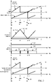
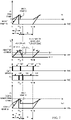
- Figure 2 illustrates timing diagrams associated with a boost operating mode under the first control mechanism in accordance with various embodiments of the present disclosure.
- the horizontal axis of Figure 2 represents intervals of time. There are five vertical axes.
- the first vertical axis Y1 represents the ramps for controlling the buck-boost converter 100.
- the second vertical axis Y2 represents the current flowing through the inductor L1 of the buck-boost converter 100.
- the third vertical axis Y3 represents the gate drive signals of switches Q1 and Q2.
- the fourth vertical axis Y4 represents the gate drive signals of switches Q3 and Q4.
- the fifth vertical axis Y5 represents a corresponding control scheme in the digital domain.
- each new switching cycle starts at the time instant t0.
- both the high-side switch Q1 of the buck converter portion and the low-side switch Q4 of the boost converter portion are turned on.
- a first ramp S1 is employed to control the operation of the buck converter portion and a second ramp S2 is employed to control the operation of the boost converter portion.
- the first ramp S1 starts from t0 and ramps up until at the end of the switching cycle.
- the first ramp S1 is reset at t3.
- t3 is the end of the switching cycle.
- the operation of the high-side switch Q1 is controlled by the first ramp S1.
- the high-side switch Q1 is turned on at t0 and remains on until the peak value of the first ramp S1 is equal to an error amplifier output voltage Vc.
- the error amplifier (not shown) has a first input coupled to the output voltage Vo of the buck-boost converter 100 and a second input connected to a reference voltage.
- the output voltage Vo is greater than the input voltage Vin.
- the intersection point (e.g ., t2) of the first ramp S1 and Vc is far beyond the end of the switching cycle determined by the inductor current. Since the first ramp S1 is reset to zero at t3 and never reaches Vc as indicated by the dashed line portion of S1, the high-side switch Q1 is not turned off and stays always on during the boost operating mode.
- the second ramp S2 includes an offset Vc0, which is a predetermined value.
- Vc0 is a predetermined value.
- the second ramp S2 starts to ramp up from Vc0 and the low-side switch Q4 of the boost converter portion is turned on.
- the low-side switch Q4 of the boost converter portion remains on until the second ramp S2 crosses the error amplifier output voltage Vc.
- the low-side switch Q4 is turned off and the second ramp S2 is reset to Vc0.
- the input voltage Vin of the buck-boost converter 100 is applied to the inductor L1.
- the inductor current ramps up from a negative value to a peak current from t0 to t1.
- the ramp-up slope of the inductor current is equal to the input voltage Vin divided by the inductance of L1.
- the current threshold iLth2 is a predetermined value. Depending on different applications and design needs, iLth2 may vary. In some embodiments, iLth2 is a negative value as shown in Figure 2 . Furthermore, iLth2 may be set to a low enough value to ensure the boost converter portion of the buck-boost converter 100 achieves ZVS at t3 and the buck converter portion of the buck-boost converter 100 achieves ZVS at the beginning of the next switching cycle. It should be noted the ZVS operation shown in Figure 2 is merely an example. There may be alternatives, variations and modifications.
- the ZVS operation can be achieved over different line and load conditions.
- the error amplifier output voltage Vc is implemented as Yn.
- Yn is in a range from 0 to 1.
- the offset Vc0 is implemented as Yn0;
- S1 and S2 are PWM ramp slopes generated by a digital power controller.
- Ts is the switching period of the buck-boost converter 100; ta is equal to Yn divided by S1; the ratio of Vo to Vin is equal to the ratio of ta to tb; tc is equal to the difference of Yn and Yn0 divided by S2.
- Yn is greater than Yn0; ta is equal to t2; tb is equal to the difference of t3 and t1; ta is equal to Ts; the sum of tb and tc is equal to Ts.
- feed-forward control mechanisms may be employed to further improve the performance (e.g ., transient response) of the boost operating mode.
- the input voltage Vin and/or the output voltage Vo may be added into the slopes.
- S1 is equal to k1 divided by Vin where k1 is a first predetermined constant.
- S2 is equal to k2 divided by Vin where k2 is a second predetermined constant.
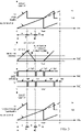
- Figure 3 illustrates timing diagrams associated with a light-load boost operating mode under the first control mechanism in accordance with various examples not falling in the scope of the claim.
- the timing diagrams shown in Figure 3 are similar to those shown in Figure 2 except that the buck-boost converter 100 operates in a light load condition.
- the light load is defined as a load less than 10% of the full load of the buck-boost converter 100. Since the ramp-up current slope and the ramp-down current slope shown in Figure 3 are the same as those shown in Figure 2 , the switching period under the light load condition shown in Figure 3 is shorter in comparison with that shown in Figure 2 in order to achieve a lower average current flowing through the inductor L1. As a result, the effective switching frequency of the buck-boost converter 100 may be relatively high for light load.
- a predetermined minimum switching period Tsmin may be implemented to limit the light load switching frequency.
- the second ramp S2 does not start to ramp until Tsmin.
- it is a delay time td in which Q4 is on and remains the on state until the second ramp S2 reaches the error amplifier output voltage Vc.
- td a delay time in which Q2 and Q4 are both turned on and the inductor current freewheels in a loop formed by L1, Q2 and Q4.
- the delay time td shown in Figure 3 is applicable to the operating mode shown in Figure 2 .
- a delay time may be added at t3.
- both the buck ramp and the boost ramp may not ramp up at t3.
- a new switching period starts at the end of the delay time td.
- control mechanism shown in Figure 3 is similar to that shown in Figure 2 , and hence is not discussed in further detail herein to avoid unnecessary repetition.
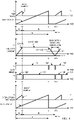
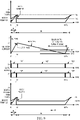
- FIG. 4 illustrates timing diagrams associated with a buck-boost operating mode under the first control mechanism in accordance with various embodiments of the present disclosure.
- Vin 48 V
- Vo 48 V
- the first ramp S1 starts from t0 and ramps up until the first ramp S1 reaches the error amplifier output voltage Vc at t2.
- the first ramp S1 is reset at t2 and starts to ramp up at the beginning of the next cycle at t3.
- the operation of the high-side switch Q1 is controlled by the first ramp S1.
- the high-side switch Q1 is turned on at t0 and remains on until the peak value of the first ramp S1 is equal to the error amplifier output voltage Vc at t2.
- the low-side switch Q2 is turned on at t2 and remains on until the end of the cycle at t3.
- the second ramp S2 includes the offset Vc0.
- the second ramp S2 starts to ramp up and the low-side switch Q4 of the boost converter portion is turned on.
- the low-side switch Q4 of the boost converter portion remains on until the peak value of the second ramp S2 is equal to the error amplifier output voltage Vc.
- the low-side switch Q4 is turned off and the second ramp S2 is reset to Vc0.
- the high-side switch Q3 is turned on and remains on until the end of the cycle at t3. It should be noted that there is a dead time between the turn-off of Q4 and the turn-on of Q3.
- the inductor current ramps up from a negative value to a peak current from t0 to t1.
- the ramp-up slope of the inductor current is equal to the input voltage Vin divided by the inductance of L1.
- Q4 is turned off and Q3 is turned on. Since both Q1 and Q3 are on, the voltage difference between Vo and Vin is applied to the inductor L1. Since the input voltage of the buck-boost converter 100 is approximately equal to the output voltage of the buck-boost converter 100, the inductor current remains relatively flat during the period from t1 to t2 as shown in Figure 4 .
- the buck stage of the buck-boost converter 100 may not achieve zero voltage switching if Q1 is turned off within the non-ZVS turn-off zone shown in Figure 4 .
- the range of the non-ZVS turn-off zone is determined by a current threshold iLth1, which is a predetermined value.
- a delay time td may be added as shown in Figure 4 .
- the delay time td may be added at t3.
- both the buck ramp and the boost ramp may not ramp up at t3.
- the buck ramp and the boost ramp may start at the end of the delay time td.
- td may vary.
- a variable td may help the buck-boost converter 100 achieve a fixed switching frequency.
- control mechanism shown in Figure 4 is similar to that shown in Figure 2 except that Ts is greater than ta as shown in Figure 4 .
- the detailed operating principle of the buck-boost operating mode in the digital control domain is not discussed herein to avoid repetition.
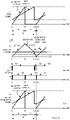
- FIG. 5 illustrates timing diagrams associated with a buck operating mode under the first control mechanism in accordance with various examples not falling in the scope of the claim.
- Vin 60 V
- Vo 8 V
- each new switching cycle starts at the time instant t0.
- the high-side switch Q1 of the buck converter portion is turned on.
- a first ramp S1 is employed to control the operation of the buck converter portion and a second ramp S2 is employed to control the operation of the boost converter portion.
- the second ramp S2 is a horizontal line with no slope since this ramp is constantly being reset to Vc0.
- the Y1-axis value of the horizontal line is equal to Vc0.
- the first ramp S1 starts from t0 and ramps up until it is reset at t2.
- the operation of the high-side switch Q1 is controlled by the first ramp S1.
- the high-side switch Q1 is turned on at t0 and remains on until the peak value of the first ramp S1 is equal to an error amplifier output voltage Vc.
- Q1 is turned off and Q2 is turned on as shown in Figure 5 .
- Vc0 is greater than Vc.
- the second ramp S2 never reaches Vc during the buck operating mode. Since the second ramp S2 never reaches Vc, the low side-switch Q4 of the boost converter portion is never on and the high-side switch Q3 of the boost converter portion stays always on during the buck operating mode.
- the inductor current ramps up from a negative value to a peak current from t0 to t2.
- the ramp-up slope of the inductor current is equal to the difference of the input voltage Vin and the output voltage Vo divided by the inductance of L1.
- a delay time td may be added as shown in Figure 5 .
- the delay time td may be added at t3.
- the buck ramp may not ramp up at t3. Instead, the buck ramp may start at the end of the delay time td.
- control mechanism shown in Figure 5 is similar to that shown in Figure 2 except that Yn0 is greater than Yn; Ts is greater than ta; Ts is equal to tb; tc is equal to zero.
- Yn0 is greater than Yn
- Ts is greater than ta
- Ts is equal to tb
- tc is equal to zero.
- the detailed operating principle of the buck operating mode in the digital control domain is not discussed herein to avoid repetition.
- t3 can be the turn-off time of the high-side switch Q3 of the boost converter portion and/or the turn-off time of the low-side switch Q2 of the buck converter portion, or the turn-off time of the high-side switch Q1 of the buck converter portion.
- the delay time td is inserted between t3 and the beginning of the following switching cycle.
- td is set to zero.
- t3 is the end of the switching period.
- the minimum switching period is greater than t3.
- td is employed to ensure the actual switching period is greater than the minimum switching period.
- the minimum switching period is a predetermined value and may vary depending on different applications and design needs.
- the switching frequency of the buck-boost converter 100 may vary depending on different line and load conditions.
- the delay time td may also be employed to achieve a fixed switching frequency under different line and load conditions.
- the transition between the buck operating mode and the buck-boost operating mode, and the transition between the boost operating mode and the buck-boost operating mode, are automatically controlled by the control loop which determines Vc, and a smooth transition can be achieved by setting appropriate values for ramps S1, S2 and Vc0.
- the operating mode transitions can be determined by comparing the input voltage Vin and the output voltage Vo. For example, according to a predetermined lookup table, the buck-boost converter 100 should enter a buck-boost operating mode when the ratio of the input voltage Vin to the output voltage Vo is equal to a value in the lookup table. At the same time, the control loop's output indicates the buck-boost converter 100 should enter a buck operating mode.
- the control scheme based upon the lookup table overrides the control scheme based upon the control loop.
- Figure 6 illustrates timing diagrams associated with a buck-boost operating mode under the second control mechanism when the output voltage is greater than the input voltage in accordance with various embodiments of the present disclosure.
- the horizontal axis of Figure 6 represents intervals of time. There are five vertical axes.
- the first vertical axis Y1 represents the ramps for controlling the buck-boost converter 100.
- the second vertical axis Y2 represents the current flowing through the inductor L1 of the buck-boost converter 100.
- the third vertical axis Y3 represents the gate drive signals of switches Q1 and Q2.
- the fourth vertical axis Y4 represents the gate drive signals of switches Q3 and Q4.
- the fifth vertical axis Y5 represents a corresponding control scheme in the digital domain.
- each new switching cycle starts at the time instant t0.
- both the high-side switch Q1 of the buck converter portion and the low-side switch Q4 of the boost converter portion are turned on.
- a first ramp S1 is employed to control the operation of the buck converter portion and a second ramp S2 is employed to control the operation of the boost converter portion.
- the first ramp S1 includes an offset Vc0, which is a predetermined value.
- the first ramp S1 starts from t0 and ramps up until the first ramp S1 reaches the error amplifier output voltage Vc at t2.
- the first ramp S1 is reset at t2 and starts to ramp up at the beginning of the next cycle.
- the operation of the high-side switch Q1 is controlled by the first ramp S1.
- the high side switch Q1 is turned on at t0 and remains on until the peak value of the first ramp S1 is equal to the error amplifier output voltage Vc at t2.
- the low-side switch Q2 is turned on at t2 and remains on until the end of the switching period at t3.
- the second ramp S2 does not include an offset and starts from zero as shown in figure 6 .
- the second ramp S2 starts to ramp up and the low-side switch Q4 of the boost converter portion is turned on.
- the low-side switch Q4 of the boost converter portion remains on until the peak value of the second ramp S2 is equal to the error amplifier output voltage Vc.
- the low-side switch Q4 is turned off and the second ramp S2 is reset to zero.
- the high-side switch Q3 is turned on and remains on until the end of the cycle at t3.
- the input voltage Vin is applied to the inductor L1.
- the inductor current ramps up from a negative value to a peak current from t0 to t1.
- the slope of the inductor current is equal to the input voltage Vin divided by the inductance of L1.
- a delay time td may be added as shown in Figure 6 .
- the delay time td may be added at t3.
- both the buck ramp and the boost ramp may not ramp up at t3. Instead, the buck ramp and the boost ramp may start at the end of the delay time td.
- control mechanism shown in Figure 6 is similar to that shown in Figure 4 except that tc is equal to Yn divided by S2 and ta is equal the difference of Yn and Yn0 divided by S1.
- Figure 6 illustrates a non-ZVS turn-off zone for Q1.
- the non-ZVS turn-off zone for Q1 shown in Figure 6 is similar to that shown in Figure 4 , and hence is not discussed herein to avoid repetition.
- Figure 7 illustrates timing diagrams associated with a light-load buck-boost operating mode under the second control mechanism when the output voltage is greater than the input voltage in accordance with various examples not falling in the scope of the claim.
- the timing diagrams shown in Figure 7 are similar to those shown in Figure 6 except that the buck-boost converter 100 operates in a light load condition. Since the inductor current ramp-up slope and the inductor current ramp-down slope are the same as those shown in Figure 6 , the switching period under the light load condition is short in comparison with that shown in Figure 6 in order to achieve a lower average current flowing through the inductor L1. As a result, the effective switching frequency of the buck-boost converter 100 is relatively high.
- a minimum switching period Tsmin may be employed. As shown in Figure 7 , the second ramp S2 does not start to ramp until Tsmin. During the period from t3 to Tsmin, it is a delay time td in which Q2 and Q4 are on and remain the on state until the end of the switching cycle.
- control mechanism shown in Figure 7 is similar to that shown in Figure 4 , and hence is not discussed herein to avoid repetition.
- the non-ZVS turn-off zone for Q1 shown in Figure 7 is similar to that shown in Figure 4 , and hence is not discussed herein to avoid repetition.
- FIG. 8 illustrates timing diagrams associated with a buck-boost operating mode under the second control mechanism when the output voltage is approximately equal to the input voltage in accordance with various embodiments of the present disclosure.
- each new switching cycle starts at the time instant t0.
- both the high-side switch Q1 of the buck converter portion and the low-side switch Q4 of the boost converter portion are turned on.
- the first ramp S1 ramps up from Vc0 until the first ramp S1 reaches the error amplifier output voltage Vc at t2.
- the first ramp S1 is reset at t2 and starts to ramp up at the beginning of the next cycle at t3.
- the operation of the high-side switch Q1 is controlled by the first ramp S1.
- the high-side switch Q1 is turned on at t0 and remains on until the peak value of the first ramp S1 is equal to an error amplifier output voltage Vc at t2.
- the low-side switch Q2 is turned on at t2 and remains on until the end of the cycle at t3.
- the second ramp S2 does not include an offset and starts from zero as shown in figure 8 .
- the second ramp S2 starts to ramp up and the low-side switch Q4 of the boost converter portion is turned on.
- the low-side switch Q4 of the boost converter portion remains on until the peak value of the second ramp S2 is equal to the error amplifier output voltage Vc.
- the low-side switch Q4 is turned off and the second ramp S2 is reset to zero.
- the high-side switch Q3 is turned on and remains on until the end of the cycle at t3.
- the input voltage Vin is applied to the inductor L1.
- the inductor current ramps up from a negative value to a peak current from t0 to t1.
- the slope of the inductor current is equal to the input voltage Vin divided by the inductance of L1.
- a delay time td may be added as shown in Figure 8 .
- the delay time td may be added at t3.
- both the buck ramp and the boost ramp may not ramp up at t3. Instead, the buck ramp and the boost ramp may start at the end of the delay time td.
- control mechanism shown in Figure 8 is similar to that shown in Figure 4 , and hence is not discussed herein to avoid repetition.
- the non-ZVS turn-off zone for Q1 shown in Figure 8 is similar to that shown in Figure 4 , and hence is not discussed herein to avoid repetition.
- FIG. 9 illustrates timing diagrams associated with a buck-boost operating mode under the second control mechanism when the input voltage is greater than the output voltage in accordance with various embodiments of the present disclosure.
- each new switching cycle starts at the time instant t0.
- both the high-side switch Q1 of the buck converter portion and the low-side switch Q4 of the boost converter are turned on.
- the first ramp S1 ramps up from Vc0 until the first ramp S1 reaches the error amplifier output voltage Vc at t2.
- the first ramp S1 is reset to Vc0 at t2 and starts to ramp up at the beginning of the next cycle.
- the operation of the high-side switch Q1 is controlled by the first ramp S1.
- the high-side switch Q1 is turned on at t0 and remains on until the peak value of the first ramp S1 is equal to the error amplifier output voltage Vc at t2.
- the low-side switch Q2 is turned on at t2 and remains on until the end of the cycle at t3.
- the second ramp S2 does not include an offset and starts from zero as shown in Figure 9 .
- the second ramp S2 starts to ramp up and the low-side switch Q4 of the boost converter portion is turned on.
- the low-side switch Q4 of the boost converter remains on until the peak value of the second ramp S2 is equal to the error amplifier output voltage Vc.
- the low-side switch Q4 is turned off and the second ramp S2 is reset to zero.
- the high side switch Q3 is turned on and remains on until the end of the cycle at t3.
- the input voltage Vin is applied to the inductor L1.
- the inductor current ramps up from a negative value to a peak current from t0 to t1.
- the slope of the inductor current is equal to the input voltage Vin divided by the inductance of L1.
- a delay time td may be added as shown in Figure 9 .
- the delay time td may be added at t3.
- both the buck ramp and the boost ramp may not ramp up at t3. Instead, the buck ramp and the boost ramp may start at the end of the delay time td.
- control mechanism shown in Figure 9 is similar to that shown in Figure 4 , and hence is not discussed herein to avoid repetition.
- the non-ZVS turn-off zone for Q1 shown in Figure 9 is similar to that shown in Figure 4 , and hence is not discussed herein to avoid repetition.
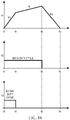
- Figure 10 illustrates timing diagrams associated with the third control mechanism in accordance with various embodiments of the present disclosure.
- the first vertical axis Y1 represents three operating phases of the buck-boost converter 100.
- the second vertical axis Y2 represents the duty cycle of the buck converter portion of the buck-boost converter 100.
- the third vertical axis Y3 represents the boost converter portion of the buck-boost converter 100.
- both the high-side switch Q1 of the buck converter portion and the low-side switch Q4 of the boost converter portion are turned on.
- the slope of the inductor current is equal to the input voltage Vin divided by the inductance of L1.
- both the high-side switch Q1 of the buck converter portion and the high-side switch Q3 of the boost converter portion are turned on.
- the slope of the inductor current is equal to the difference of the input voltage Vin and output voltage Vo divided by the inductance of L1.
- both the low-side switch Q2 of the buck converter portion and the high-side switch Q3 of the boost converter portion are turned on.
- the slope of the inductor current is equal to the output voltage Vo divided by the inductance of L1.
- the turning point of the first phase P1 and the second phase P2 is t1.
- the turning point of the second phase P2 and the third phase P3 is t2.
- the duty cycle of the buck converter portion is equal to t2 divided by Ts where Ts is the switching period of the buck-boost converter 100.
- the duty cycle of the boost converter portion is equal to t1 divided by Ts. Ts is determined by the inductor current crossing a predetermined threshold (e.g., iLth2).
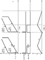
- Figure 11 illustrates timing diagrams associated with a buck operating mode under the third control mechanism shown in Figure 10 in accordance with various examples not in the scope of the claim.
- the boost converter portion operates in a fixed duty cycle mode.
- the time of the first phase P1 is equal to the minimum on-time of the low-side switch Q4 of the boost converter portion.
- the minimum on-time Tmin_on of the low-side switch Q4 is equal to 100 ns.
- the duty cycle of the buck converter portion is determined by the intersection point of a buck ramp S1 and an error amplifier output voltage Vc. As shown in Figure 11 , when the buck ramp S1 reaches Vc, the turn-on of Q1 of the buck converter portion terminates.
- the duty cycle of the buck converter portion is adjustable through varying the error amplifier output voltage Vc as shown in Figure 11 .
- Figure 12 illustrates timing diagrams associated with a buck-boost operating mode under the third control mechanism shown in Figure 10 in accordance with various examples not within the scope of the claim.
- the duty cycle of the boost converter portion is determined by the intersection point of a boost ramp S2 and the error amplifier output voltage Vc. As shown in Figure 12 , when the boost ramp S2 reaches Vc, the turn-on of the low-side switch Q4 of the boost converter portion terminates.
- the duty cycle of the boost converter portion is adjustable through varying the error amplifier output voltage Vc as shown in Figure 12 .
- the duty cycle of the buck converter portion is determined by a buck ramp S1 and the error amplifier output voltage Vc. As shown in Figure 12 , when the buck ramp S1 reaches Vc, the turn-on of the high-side switch Q1 of the buck converter portion terminates.
- Figure 13 illustrates timing diagrams associated with a boost operating mode under the third control mechanism shown in Figure 10 in accordance with various examples not within the scope of the claim.
- the duty cycle of the boost converter portion is determined by a boost ramp S2 and the error amplifier output voltage Vc. As shown in Figure 13 , when the boost ramp S2 reaches Vc, the turn-on of the low-side switch Q3 of the boost converter portion terminates.
- the duty cycle of the boost converter portion is adjustable through varying the error amplifier output voltage Vc as shown in Figure 13 .
- the buck ramp S1 never reaches the error amplifier output voltage Vc before the switching cycle ends. Therefore, as shown in Figure 13 , the high-side switch Q1 of the buck converter portion is always on.
- the error amplifier output voltage Vc shown in Figures 11-13 is implemented as Yn.
- Yn is in a range from 0 to 1.
- Ts is the switching cycle of the buck-boost converter 100.
- a mode selection threshold Yth is predetermined. In some embodiments, the mode selection threshold Yth is set to 0.4.
- the buck-boost converter 100 when Yn is in a range from 0 to Yth, the buck-boost converter 100 operates in the buck operating mode as shown in Figure 11 .
- the time of the first phase P1 is equal to the minimum on-time Tmin_on of the low-side switch Q4 of the boost converter portion.
- the buck-boost converter 100 When Yn is in a range from Yth to 1, the buck-boost converter 100 operates in the buck-boost operating mode shown in Figure 12 .
- the total time of P1 and P2 is a fixed value.
- P1 Ton _ min + k 2 ⁇ Yn ⁇ Yth ⁇ T s max where k2 is a predetermined constant and Ton_min is the minimum on-time of the low-side switch Q4 of the boost converter portion.
- the buck-boost converter 100 When Yn goes even higher in the range from Yth to 1, the buck-boost converter 100 will move into the boost operating mode shown in Figure 13 .
- the output voltage Vo of the buck-boost converter 100 is much greater than the input voltage Vin of the buck-boost converter 100, the current flowing through the inductor L1 drops much quicker to the negative current threshold and a new switching cycle begins before the second phase P2 finishes.
- the third phase P3 does not exist as shown in Figure 13 .
- the buck-boost converter 100 operates in the boost operating mode.
- the buck-boost converter 100 operates in the buck-boost operating mode.
- the buck converter portion operates at a duty defined by Equation (2).
Landscapes
- Engineering & Computer Science (AREA)
- Power Engineering (AREA)
- Dc-Dc Converters (AREA)
Claims (1)
- Verfahren, das Folgendes umfasst:Erzeugen eines ersten Rampensignals (S1) zum Steuern eines Abwärtswandlerteils eines Abwärts-/Aufwärtswandlers (100), wobei der Abwärts-/Aufwärtswandler (100) Folgendes umfasst:einen ersten "High-Side"-Schalter (Q1) und einen ersten "Low-Side"-Schalter (Q2), die über einen Eingangskondensator (CIN) in Reihe geschaltet sind;einen zweiten "High-Side"-Schalter (Q3) und einen zweiten "Low-Side"-Schalter (Q4), die über einen Ausgangskondensator (Co) in Reihe geschaltet sind; undeine Spule (L1), die zwischen einen gemeinsamen Knoten des ersten "High-Side"-Schalters (Q1) und des ersten "Low-Side"-Schalters (Q2) und einen gemeinsamen Knoten des zweiten "High-Side"-Schalters (Q3) und des zweiten "Low-Side"-Schalters (Q4) gekoppelt ist;Erzeugen eines zweiten Rampensignals (S2) zum Steuern eines Aufwärtswandlerteils des Abwärts-/Aufwärtswandlers (100);Vergleichen des ersten Rampensignals (S1) und des zweiten Rampensignals (S2) mit einem Steuersignal;Steuern eines Zustands des ersten "High-Side"-Schalters (Q1) unter Nutzung des Vergleichs des ersten Rampensignals (S1) mit dem Steuersignal und eines Zustands des zweiten "Low-Side"-Schalters (Q4) unter Nutzung des Vergleichs des zweiten Rampensignals (S2) mit dem Steuersignal;Vergleichen eines durch die Spule (L1) fließenden Stroms mit einem Stromschwellenwert; undBeenden eines Schaltzyklus basierend auf dem Vergleich des durch die Spule (L1) fließenden Stroms mit dem Stromschwellenwert;Addieren eines Offsets zum ersten Rampensignal (S1) oder zum zweiten Rampensignal (S2);dadurch gekennzeichnet, dass das Verfahren ferner Folgendes umfasst:
als Reaktion darauf, dass eine abzugebende Ausgangsspannung (Vo) ungefähr gleich einer Eingangsspannung (Vin) des Abwärts-/Aufwärtswandlers (100) ist:Abschalten des zweiten "Low-Side"-Schalters (Q4), Einschalten des zweiten "High-Side"-Schalters (Q3) und Zurücksetzen des zweiten Rampensignals (S2) auf seinen Ausgangswert, wenn das zweite Rampensignal (S2) gleich dem Steuersignal ist;Abschalten des ersten "High-Side"-Schalters (Q1), Einschalten des ersten "Low-Side"-Schalters (Q2) und Zurücksetzen des ersten Rampensignals (S1) auf seinen Ausgangswert, wenn das erste Rampensignal (S1) gleich dem Steuersignal ist;Abschalten des ersten "Low-Side"-Schalters (Q2) und des zweiten "High-Side"-Schalters (Q3) und Einschalten des ersten "High-Side"-Schalters (Q1) und des zweiten "Low-Side"-Schalters (Q4), wenn der durch die Spule (L1) fließende Strom gleich dem Stromschwellenwert ist, wodurch der Schaltzyklus beendet wird.
Applications Claiming Priority (2)
| Application Number | Priority Date | Filing Date | Title |
|---|---|---|---|
| US14/739,827 US10177661B2 (en) | 2015-06-15 | 2015-06-15 | Control method for buck-boost power converters |
| PCT/CN2016/085746 WO2016202244A1 (en) | 2015-06-15 | 2016-06-14 | Control method for buck-boost power converters |
Publications (3)
| Publication Number | Publication Date |
|---|---|
| EP3198710A1 EP3198710A1 (de) | 2017-08-02 |
| EP3198710A4 EP3198710A4 (de) | 2017-10-25 |
| EP3198710B1 true EP3198710B1 (de) | 2022-05-25 |
Family
ID=57517340
Family Applications (1)
| Application Number | Title | Priority Date | Filing Date |
|---|---|---|---|
| EP16810985.8A Active EP3198710B1 (de) | 2015-06-15 | 2016-06-14 | Steuerungsverfahren für aufwärts-abwärts-wandler |
Country Status (4)
| Country | Link |
|---|---|
| US (2) | US10177661B2 (de) |
| EP (1) | EP3198710B1 (de) |
| CN (1) | CN107534387B (de) |
| WO (1) | WO2016202244A1 (de) |
Families Citing this family (29)
| Publication number | Priority date | Publication date | Assignee | Title |
|---|---|---|---|---|
| US10454371B1 (en) * | 2015-05-08 | 2019-10-22 | Maxim Integrated Products, Inc. | High efficiency buck-boost systems and methods |
| US10141845B2 (en) | 2016-04-13 | 2018-11-27 | Texas Instruments Incorporated | DC-DC converter and control circuit with low-power clocked comparator referenced to switching node for zero voltage switching |
| US10177658B2 (en) | 2016-04-14 | 2019-01-08 | Texas Instruments Incorporated | Methods and apparatus for adaptive timing for zero voltage transition power converters |
| US10141846B2 (en) | 2016-04-15 | 2018-11-27 | Texas Instruments Incorporated | Methods and apparatus for adaptive timing for zero voltage transition power converters |
| US20170373600A1 (en) * | 2016-06-23 | 2017-12-28 | Cirrus Logic International Semiconductor Ltd. | Multi-mode switching power converter |
| US10826325B2 (en) * | 2018-02-21 | 2020-11-03 | X2 Power Technologies Limited | Hybrid control apparatus and method |
| US10644600B2 (en) * | 2018-03-25 | 2020-05-05 | Richtek Technology Corporation | Constant-time buck-boost switching regulator and control circuit and control method thereof |
| IT201800008221A1 (it) * | 2018-08-29 | 2020-02-29 | St Microelectronics Srl | Convertitore elettronico, circuito integrato e procedimento di funzionamento di un convertitore elettronico corrispondenti |
| US10840797B2 (en) | 2018-11-26 | 2020-11-17 | Texas Instruments Incorporated | Load release detection circuit |
| US10958173B2 (en) * | 2018-12-26 | 2021-03-23 | Texas Instruments Incorporated | Fixed frequency buck-boost power converter control |
| KR102199760B1 (ko) * | 2019-02-26 | 2021-01-07 | 효성중공업 주식회사 | 직류 컨버터 장치 |
| WO2020243891A1 (en) * | 2019-06-04 | 2020-12-10 | Abb Schweiz Ag | Apparatus and method for power conversion |
| CN110071557A (zh) * | 2019-06-12 | 2019-07-30 | 海矽微(厦门)电子有限公司 | 一种电池充电架构 |
| IT201900014715A1 (it) | 2019-08-13 | 2021-02-13 | St Microelectronics Srl | Dispositivo di controllo per regolatore di tensione a commutazione e metodo di controllo |
| DE102019212351A1 (de) * | 2019-08-19 | 2021-02-25 | Robert Bosch Gmbh | Batteriesystem für ein Kraftfahrzeug, Verfahren zum Betreiben eines Batteriesystems und Kraftfahrzeug |
| US11342846B2 (en) | 2019-09-20 | 2022-05-24 | Texas Instruments Incorporated | Digital control for voltage converter |
| CN110768528B (zh) * | 2019-11-13 | 2020-11-10 | 清华大学 | 一种用于非反向Buck-Boost电路工作模式平滑切换的控制方法 |
| EP3905498A1 (de) * | 2020-04-28 | 2021-11-03 | Siemens Aktiengesellschaft | Verfahren zum regeln eines tief-hochsetzstellers |
| CN111969877B (zh) * | 2020-06-23 | 2021-07-02 | 湖南大学 | 一种半桥逆变器的控制方法及装置 |
| CN113938008B (zh) * | 2020-06-29 | 2023-12-22 | 中兴通讯股份有限公司 | 双向dc变换器及其控制方法、控制模块、存储介质 |
| US11522458B2 (en) * | 2020-09-02 | 2022-12-06 | Cypress Semiconductor Corporation | Bootstrap voltage refresh for buck-boost converter |
| CN112583279B (zh) * | 2020-12-15 | 2022-03-01 | 武汉葆源新能科技有限公司 | 一种适用于双向隔离型dcdc变换器的控制方法及系统 |
| US11682972B2 (en) * | 2021-02-04 | 2023-06-20 | Analog Devices, Inc. | Peak current mode control for buck-boost regulators |
| CN112994452B (zh) * | 2021-04-26 | 2021-08-03 | 上海南芯半导体科技有限公司 | 一种带有模式切换的升降压变换器控制电路 |
| US11770072B2 (en) * | 2021-10-26 | 2023-09-26 | Allegro Microsystems, Llc | Commonly controlled buck-boost converter |
| CN116032120A (zh) * | 2021-10-27 | 2023-04-28 | 北京大瞬科技有限公司 | 直流/直流转换器及用于直流/直流转换器的控制方法 |
| CN114221543B (zh) * | 2021-11-25 | 2024-05-24 | 西安领充创享新能源科技有限公司 | H桥四开关电路的控制方法及双向充放电装置 |
| CN115065244B (zh) * | 2022-07-05 | 2025-11-04 | 上海杰瑞兆新信息科技有限公司 | 四开关升降压变换器的控制电路及优化方法 |
| TWI876730B (zh) * | 2023-12-01 | 2025-03-11 | 立錡科技股份有限公司 | 可防突波的切換式轉換電路 |
Family Cites Families (26)
| Publication number | Priority date | Publication date | Assignee | Title |
|---|---|---|---|---|
| US6166527A (en) * | 2000-03-27 | 2000-12-26 | Linear Technology Corporation | Control circuit and method for maintaining high efficiency in a buck-boost switching regulator |
| US6329801B1 (en) * | 2000-04-24 | 2001-12-11 | Volterra Semiconductor Corporation | Switching regulator control system and method |
| US6984967B2 (en) * | 2003-10-29 | 2006-01-10 | Allegro Microsystems, Inc. | Multi-mode switching regulator |
| JP4381327B2 (ja) * | 2005-03-02 | 2009-12-09 | 富士通マイクロエレクトロニクス株式会社 | Dc−dcコンバータ、dc−dcコンバータ制御装置、電源装置、電子装置及びdc−dcコンバータ制御方法 |
| US7157888B2 (en) * | 2005-06-06 | 2007-01-02 | Aimtron Technology Corp. | Light loading control circuit for a buck-boost voltage converter |
| US7528587B2 (en) * | 2005-12-27 | 2009-05-05 | Linear Technology Corporation | Switched converter with variable peak current and variable off-time control |
| US7518346B2 (en) * | 2006-03-03 | 2009-04-14 | Texas Instruments Deutschland Gmbh | Buck-boost DC/DC converter with overlap control using ramp shift signal |
| US7453247B2 (en) * | 2006-06-30 | 2008-11-18 | Analog Devices, Inc. | DC to DC voltage converter |
| US8319483B2 (en) * | 2007-08-06 | 2012-11-27 | Solaredge Technologies Ltd. | Digital average input current control in power converter |
| JP2009027895A (ja) | 2007-07-24 | 2009-02-05 | Hitachi Ltd | スイッチング電源 |
| US8143865B2 (en) * | 2008-08-22 | 2012-03-27 | Active-Semi, Inc. | Average current mode controlled converter having a buck mode, a boost mode, and a partial four-switch mode |
| EP2189870A1 (de) | 2008-11-25 | 2010-05-26 | St Microelectronics S.A. | Spannungsschaltregler |
| KR101585958B1 (ko) * | 2008-12-29 | 2016-01-18 | 주식회사 동부하이텍 | 기준전압 발생회로 |
| CN101944850B (zh) | 2009-07-06 | 2013-07-31 | 立锜科技股份有限公司 | 升降压切换式电源电路与其控制电路与方法 |
| US8773084B2 (en) * | 2009-08-24 | 2014-07-08 | Micrel, Inc. | Buck-boost converter using timers for mode transition control |
| TWI422127B (zh) * | 2009-09-29 | 2014-01-01 | Richtek Technology Corp | 升降壓式電源轉換器的控制電路及方法 |
| US8330435B2 (en) | 2009-10-15 | 2012-12-11 | Intersil Americas Inc. | Hysteretic controlled buck-boost converter |
| US9035626B2 (en) * | 2010-08-18 | 2015-05-19 | Volterra Semiconductor Corporation | Switching circuits for extracting power from an electric power source and associated methods |
| US8334683B2 (en) * | 2010-08-24 | 2012-12-18 | Intersil Americas Inc. | System and method for current limiting a DC-DC converter |
| US8957644B2 (en) | 2010-08-25 | 2015-02-17 | Futurewei Technologies, Inc. | High efficiency high power density power architecture based on buck-boost regulators with a pass-through band |
| TWI404309B (zh) * | 2010-12-09 | 2013-08-01 | Richtek Technology Corp | 切換式升降壓轉換器控制電路及方法 |
| EP2466740B1 (de) * | 2010-12-14 | 2020-02-05 | Dialog Semiconductor GmbH | Schaltung eines Hochleistungs-Tief-Hochsetzsperrwandlers und Steuerungsverfahren dafür |
| CN102694469A (zh) | 2012-05-21 | 2012-09-26 | 成都芯源系统有限公司 | 直流-直流电压转换器 |
| US8841895B2 (en) * | 2012-06-04 | 2014-09-23 | Texas Instruments Deutschland Gmbh | Electronic device for average current mode DC-DC conversion |
| US9362828B2 (en) * | 2013-02-06 | 2016-06-07 | Microsemi Corporation | Hysteretic current mode control converter with low, medium and high current thresholds |
| CN103280971B (zh) * | 2013-05-28 | 2016-01-13 | 成都芯源系统有限公司 | 升降压变换器及其控制器和控制方法 |
-
2015
- 2015-06-15 US US14/739,827 patent/US10177661B2/en active Active
-
2016
- 2016-06-14 EP EP16810985.8A patent/EP3198710B1/de active Active
- 2016-06-14 WO PCT/CN2016/085746 patent/WO2016202244A1/en not_active Ceased
- 2016-06-14 CN CN201680021583.3A patent/CN107534387B/zh active Active
-
2018
- 2018-12-07 US US16/212,943 patent/US10554130B2/en active Active
Also Published As
| Publication number | Publication date |
|---|---|
| WO2016202244A1 (en) | 2016-12-22 |
| EP3198710A1 (de) | 2017-08-02 |
| US20160365790A1 (en) | 2016-12-15 |
| CN107534387B (zh) | 2020-05-08 |
| EP3198710A4 (de) | 2017-10-25 |
| US10554130B2 (en) | 2020-02-04 |
| US10177661B2 (en) | 2019-01-08 |
| CN107534387A (zh) | 2018-01-02 |
| US20190123650A1 (en) | 2019-04-25 |
Similar Documents
| Publication | Publication Date | Title |
|---|---|---|
| EP3198710B1 (de) | Steuerungsverfahren für aufwärts-abwärts-wandler | |
| US11870350B2 (en) | Switched-mode power controller with multi-mode startup | |
| CN111835216B (zh) | 防止开关变换器的整流器中电流反向的控制方法与系统 | |
| US9614447B2 (en) | Control circuits and methods for active-clamp flyback power converters | |
| US9906147B2 (en) | Adaptive dead time control apparatus and method for switching power converters | |
| JP6634089B2 (ja) | ソフトスイッチングフライバックコンバータ | |
| EP2421137B1 (de) | Schaltnetzteileinheit | |
| US9705413B2 (en) | Multi-mode operation and control of a resonant converter | |
| US9431896B2 (en) | Apparatus and method for zero voltage switching in bridgeless totem pole power factor correction converter | |
| US7385833B2 (en) | Snubber circuit for a power converter | |
| US10476372B2 (en) | Buck-boost power converter and method of operation thereof | |
| US10158290B2 (en) | Semi-resonant and resonant converters and method of control | |
| US9793810B2 (en) | Control method for zero voltage switching buck-boost power converters | |
| US9935547B2 (en) | System and method for a switched-mode power supply | |
| EP3393027A1 (de) | Sanftschaltung für hochfrequente leistungsumwandlung | |
| JPWO2016139745A1 (ja) | 電力変換器 | |
| EP3509203A1 (de) | Umrichter mit nullspannungsschaltung | |
| US20080259649A1 (en) | Switched mode power supply comprising a rectifier circuit | |
| US8503195B1 (en) | System and method for zero volt switching of half bridge converters during startup and short circuit conditions | |
| EP2532083B1 (de) | Stromwandler | |
| US11075582B2 (en) | Switching converter | |
| EP4131758A1 (de) | Resonanzwandlersystem mit sanftem anlauf und ausgangsspannungsregelung sowie steuerverfahren dafür | |
| Yahaya et al. | Experimental analysis of a new zero-voltage switching synchronous rectifier buck converter | |
| EP1983639A1 (de) | Schaltnetzteil mit Gleichrichterschaltung |
Legal Events
| Date | Code | Title | Description |
|---|---|---|---|
| STAA | Information on the status of an ep patent application or granted ep patent |
Free format text: STATUS: THE INTERNATIONAL PUBLICATION HAS BEEN MADE |
|
| PUAI | Public reference made under article 153(3) epc to a published international application that has entered the european phase |
Free format text: ORIGINAL CODE: 0009012 |
|
| STAA | Information on the status of an ep patent application or granted ep patent |
Free format text: STATUS: REQUEST FOR EXAMINATION WAS MADE |
|
| 17P | Request for examination filed |
Effective date: 20170426 |
|
| AK | Designated contracting states |
Kind code of ref document: A1 Designated state(s): AL AT BE BG CH CY CZ DE DK EE ES FI FR GB GR HR HU IE IS IT LI LT LU LV MC MK MT NL NO PL PT RO RS SE SI SK SM TR |
|
| AX | Request for extension of the european patent |
Extension state: BA ME |
|
| A4 | Supplementary search report drawn up and despatched |
Effective date: 20170927 |
|
| RIC1 | Information provided on ipc code assigned before grant |
Ipc: H02M 1/00 20070101ALN20170921BHEP Ipc: H02M 3/158 20060101AFI20170921BHEP |
|
| RIN1 | Information on inventor provided before grant (corrected) |
Inventor name: YE, LIMING Inventor name: CHEN, DAOSHEN Inventor name: FU, DIANBO Inventor name: DAI, HEPING Inventor name: HUANG, JINBO |
|
| DAV | Request for validation of the european patent (deleted) | ||
| DAX | Request for extension of the european patent (deleted) | ||
| STAA | Information on the status of an ep patent application or granted ep patent |
Free format text: STATUS: EXAMINATION IS IN PROGRESS |
|
| 17Q | First examination report despatched |
Effective date: 20190902 |
|
| RAP1 | Party data changed (applicant data changed or rights of an application transferred) |
Owner name: HUAWEI DIGITAL POWER TECHNOLOGIES CO., LTD. |
|
| REG | Reference to a national code |
Ref country code: DE Ref legal event code: R079 Ref document number: 602016072406 Country of ref document: DE Free format text: PREVIOUS MAIN CLASS: H02M0003155000 Ipc: H02M0003158000 |
|
| GRAP | Despatch of communication of intention to grant a patent |
Free format text: ORIGINAL CODE: EPIDOSNIGR1 |
|
| STAA | Information on the status of an ep patent application or granted ep patent |
Free format text: STATUS: GRANT OF PATENT IS INTENDED |
|
| RIC1 | Information provided on ipc code assigned before grant |
Ipc: H02M 1/00 20060101ALN20211218BHEP Ipc: H02M 3/158 20060101AFI20211218BHEP |
|
| RIC1 | Information provided on ipc code assigned before grant |
Ipc: H02M 1/00 20060101ALN20220110BHEP Ipc: H02M 3/158 20060101AFI20220110BHEP |
|
| INTG | Intention to grant announced |
Effective date: 20220124 |
|
| GRAS | Grant fee paid |
Free format text: ORIGINAL CODE: EPIDOSNIGR3 |
|
| GRAA | (expected) grant |
Free format text: ORIGINAL CODE: 0009210 |
|
| STAA | Information on the status of an ep patent application or granted ep patent |
Free format text: STATUS: THE PATENT HAS BEEN GRANTED |
|
| AK | Designated contracting states |
Kind code of ref document: B1 Designated state(s): AL AT BE BG CH CY CZ DE DK EE ES FI FR GB GR HR HU IE IS IT LI LT LU LV MC MK MT NL NO PL PT RO RS SE SI SK SM TR |
|
| REG | Reference to a national code |
Ref country code: GB Ref legal event code: FG4D |
|
| REG | Reference to a national code |
Ref country code: CH Ref legal event code: EP |
|
| REG | Reference to a national code |
Ref country code: AT Ref legal event code: REF Ref document number: 1494643 Country of ref document: AT Kind code of ref document: T Effective date: 20220615 Ref country code: DE Ref legal event code: R096 Ref document number: 602016072406 Country of ref document: DE |
|
| REG | Reference to a national code |
Ref country code: IE Ref legal event code: FG4D |
|
| REG | Reference to a national code |
Ref country code: LT Ref legal event code: MG9D |
|
| REG | Reference to a national code |
Ref country code: NL Ref legal event code: MP Effective date: 20220525 |
|
| REG | Reference to a national code |
Ref country code: AT Ref legal event code: MK05 Ref document number: 1494643 Country of ref document: AT Kind code of ref document: T Effective date: 20220525 |
|
| PG25 | Lapsed in a contracting state [announced via postgrant information from national office to epo] |
Ref country code: SE Free format text: LAPSE BECAUSE OF FAILURE TO SUBMIT A TRANSLATION OF THE DESCRIPTION OR TO PAY THE FEE WITHIN THE PRESCRIBED TIME-LIMIT Effective date: 20220525 Ref country code: PT Free format text: LAPSE BECAUSE OF FAILURE TO SUBMIT A TRANSLATION OF THE DESCRIPTION OR TO PAY THE FEE WITHIN THE PRESCRIBED TIME-LIMIT Effective date: 20220926 Ref country code: NO Free format text: LAPSE BECAUSE OF FAILURE TO SUBMIT A TRANSLATION OF THE DESCRIPTION OR TO PAY THE FEE WITHIN THE PRESCRIBED TIME-LIMIT Effective date: 20220825 Ref country code: NL Free format text: LAPSE BECAUSE OF FAILURE TO SUBMIT A TRANSLATION OF THE DESCRIPTION OR TO PAY THE FEE WITHIN THE PRESCRIBED TIME-LIMIT Effective date: 20220525 Ref country code: LT Free format text: LAPSE BECAUSE OF FAILURE TO SUBMIT A TRANSLATION OF THE DESCRIPTION OR TO PAY THE FEE WITHIN THE PRESCRIBED TIME-LIMIT Effective date: 20220525 Ref country code: HR Free format text: LAPSE BECAUSE OF FAILURE TO SUBMIT A TRANSLATION OF THE DESCRIPTION OR TO PAY THE FEE WITHIN THE PRESCRIBED TIME-LIMIT Effective date: 20220525 Ref country code: GR Free format text: LAPSE BECAUSE OF FAILURE TO SUBMIT A TRANSLATION OF THE DESCRIPTION OR TO PAY THE FEE WITHIN THE PRESCRIBED TIME-LIMIT Effective date: 20220826 Ref country code: FI Free format text: LAPSE BECAUSE OF FAILURE TO SUBMIT A TRANSLATION OF THE DESCRIPTION OR TO PAY THE FEE WITHIN THE PRESCRIBED TIME-LIMIT Effective date: 20220525 Ref country code: ES Free format text: LAPSE BECAUSE OF FAILURE TO SUBMIT A TRANSLATION OF THE DESCRIPTION OR TO PAY THE FEE WITHIN THE PRESCRIBED TIME-LIMIT Effective date: 20220525 Ref country code: BG Free format text: LAPSE BECAUSE OF FAILURE TO SUBMIT A TRANSLATION OF THE DESCRIPTION OR TO PAY THE FEE WITHIN THE PRESCRIBED TIME-LIMIT Effective date: 20220825 Ref country code: AT Free format text: LAPSE BECAUSE OF FAILURE TO SUBMIT A TRANSLATION OF THE DESCRIPTION OR TO PAY THE FEE WITHIN THE PRESCRIBED TIME-LIMIT Effective date: 20220525 |
|
| PG25 | Lapsed in a contracting state [announced via postgrant information from national office to epo] |
Ref country code: RS Free format text: LAPSE BECAUSE OF FAILURE TO SUBMIT A TRANSLATION OF THE DESCRIPTION OR TO PAY THE FEE WITHIN THE PRESCRIBED TIME-LIMIT Effective date: 20220525 Ref country code: PL Free format text: LAPSE BECAUSE OF FAILURE TO SUBMIT A TRANSLATION OF THE DESCRIPTION OR TO PAY THE FEE WITHIN THE PRESCRIBED TIME-LIMIT Effective date: 20220525 Ref country code: LV Free format text: LAPSE BECAUSE OF FAILURE TO SUBMIT A TRANSLATION OF THE DESCRIPTION OR TO PAY THE FEE WITHIN THE PRESCRIBED TIME-LIMIT Effective date: 20220525 Ref country code: IS Free format text: LAPSE BECAUSE OF FAILURE TO SUBMIT A TRANSLATION OF THE DESCRIPTION OR TO PAY THE FEE WITHIN THE PRESCRIBED TIME-LIMIT Effective date: 20220925 |
|
| PG25 | Lapsed in a contracting state [announced via postgrant information from national office to epo] |
Ref country code: SM Free format text: LAPSE BECAUSE OF FAILURE TO SUBMIT A TRANSLATION OF THE DESCRIPTION OR TO PAY THE FEE WITHIN THE PRESCRIBED TIME-LIMIT Effective date: 20220525 Ref country code: SK Free format text: LAPSE BECAUSE OF FAILURE TO SUBMIT A TRANSLATION OF THE DESCRIPTION OR TO PAY THE FEE WITHIN THE PRESCRIBED TIME-LIMIT Effective date: 20220525 Ref country code: RO Free format text: LAPSE BECAUSE OF FAILURE TO SUBMIT A TRANSLATION OF THE DESCRIPTION OR TO PAY THE FEE WITHIN THE PRESCRIBED TIME-LIMIT Effective date: 20220525 Ref country code: EE Free format text: LAPSE BECAUSE OF FAILURE TO SUBMIT A TRANSLATION OF THE DESCRIPTION OR TO PAY THE FEE WITHIN THE PRESCRIBED TIME-LIMIT Effective date: 20220525 Ref country code: DK Free format text: LAPSE BECAUSE OF FAILURE TO SUBMIT A TRANSLATION OF THE DESCRIPTION OR TO PAY THE FEE WITHIN THE PRESCRIBED TIME-LIMIT Effective date: 20220525 Ref country code: CZ Free format text: LAPSE BECAUSE OF FAILURE TO SUBMIT A TRANSLATION OF THE DESCRIPTION OR TO PAY THE FEE WITHIN THE PRESCRIBED TIME-LIMIT Effective date: 20220525 |
|
| REG | Reference to a national code |
Ref country code: CH Ref legal event code: PL |
|
| REG | Reference to a national code |
Ref country code: BE Ref legal event code: MM Effective date: 20220630 |
|
| PG25 | Lapsed in a contracting state [announced via postgrant information from national office to epo] |
Ref country code: MC Free format text: LAPSE BECAUSE OF FAILURE TO SUBMIT A TRANSLATION OF THE DESCRIPTION OR TO PAY THE FEE WITHIN THE PRESCRIBED TIME-LIMIT Effective date: 20220525 |
|
| REG | Reference to a national code |
Ref country code: DE Ref legal event code: R097 Ref document number: 602016072406 Country of ref document: DE |
|
| PG25 | Lapsed in a contracting state [announced via postgrant information from national office to epo] |
Ref country code: AL Free format text: LAPSE BECAUSE OF FAILURE TO SUBMIT A TRANSLATION OF THE DESCRIPTION OR TO PAY THE FEE WITHIN THE PRESCRIBED TIME-LIMIT Effective date: 20220525 |
|
| PLBE | No opposition filed within time limit |
Free format text: ORIGINAL CODE: 0009261 |
|
| STAA | Information on the status of an ep patent application or granted ep patent |
Free format text: STATUS: NO OPPOSITION FILED WITHIN TIME LIMIT |
|
| GBPC | Gb: european patent ceased through non-payment of renewal fee |
Effective date: 20220825 |
|
| PG25 | Lapsed in a contracting state [announced via postgrant information from national office to epo] |
Ref country code: LU Free format text: LAPSE BECAUSE OF NON-PAYMENT OF DUE FEES Effective date: 20220614 Ref country code: LI Free format text: LAPSE BECAUSE OF NON-PAYMENT OF DUE FEES Effective date: 20220630 Ref country code: IE Free format text: LAPSE BECAUSE OF NON-PAYMENT OF DUE FEES Effective date: 20220614 Ref country code: FR Free format text: LAPSE BECAUSE OF NON-PAYMENT OF DUE FEES Effective date: 20220725 Ref country code: CH Free format text: LAPSE BECAUSE OF NON-PAYMENT OF DUE FEES Effective date: 20220630 |
|
| 26N | No opposition filed |
Effective date: 20230228 |
|
| PG25 | Lapsed in a contracting state [announced via postgrant information from national office to epo] |
Ref country code: SI Free format text: LAPSE BECAUSE OF FAILURE TO SUBMIT A TRANSLATION OF THE DESCRIPTION OR TO PAY THE FEE WITHIN THE PRESCRIBED TIME-LIMIT Effective date: 20220525 Ref country code: BE Free format text: LAPSE BECAUSE OF NON-PAYMENT OF DUE FEES Effective date: 20220630 |
|
| P01 | Opt-out of the competence of the unified patent court (upc) registered |
Effective date: 20230524 |
|
| PG25 | Lapsed in a contracting state [announced via postgrant information from national office to epo] |
Ref country code: GB Free format text: LAPSE BECAUSE OF NON-PAYMENT OF DUE FEES Effective date: 20220825 |
|
| PG25 | Lapsed in a contracting state [announced via postgrant information from national office to epo] |
Ref country code: IT Free format text: LAPSE BECAUSE OF FAILURE TO SUBMIT A TRANSLATION OF THE DESCRIPTION OR TO PAY THE FEE WITHIN THE PRESCRIBED TIME-LIMIT Effective date: 20220525 |
|
| PG25 | Lapsed in a contracting state [announced via postgrant information from national office to epo] |
Ref country code: HU Free format text: LAPSE BECAUSE OF FAILURE TO SUBMIT A TRANSLATION OF THE DESCRIPTION OR TO PAY THE FEE WITHIN THE PRESCRIBED TIME-LIMIT; INVALID AB INITIO Effective date: 20160614 |
|
| PG25 | Lapsed in a contracting state [announced via postgrant information from national office to epo] |
Ref country code: MK Free format text: LAPSE BECAUSE OF FAILURE TO SUBMIT A TRANSLATION OF THE DESCRIPTION OR TO PAY THE FEE WITHIN THE PRESCRIBED TIME-LIMIT Effective date: 20220525 Ref country code: CY Free format text: LAPSE BECAUSE OF FAILURE TO SUBMIT A TRANSLATION OF THE DESCRIPTION OR TO PAY THE FEE WITHIN THE PRESCRIBED TIME-LIMIT Effective date: 20220525 |
|
| PG25 | Lapsed in a contracting state [announced via postgrant information from national office to epo] |
Ref country code: MT Free format text: LAPSE BECAUSE OF FAILURE TO SUBMIT A TRANSLATION OF THE DESCRIPTION OR TO PAY THE FEE WITHIN THE PRESCRIBED TIME-LIMIT Effective date: 20220525 |
|
| PG25 | Lapsed in a contracting state [announced via postgrant information from national office to epo] |
Ref country code: BG Free format text: LAPSE BECAUSE OF FAILURE TO SUBMIT A TRANSLATION OF THE DESCRIPTION OR TO PAY THE FEE WITHIN THE PRESCRIBED TIME-LIMIT Effective date: 20220525 |
|
| PG25 | Lapsed in a contracting state [announced via postgrant information from national office to epo] |
Ref country code: BG Free format text: LAPSE BECAUSE OF FAILURE TO SUBMIT A TRANSLATION OF THE DESCRIPTION OR TO PAY THE FEE WITHIN THE PRESCRIBED TIME-LIMIT Effective date: 20220525 |
|
| PGFP | Annual fee paid to national office [announced via postgrant information from national office to epo] |
Ref country code: DE Payment date: 20250429 Year of fee payment: 10 |
|
| PG25 | Lapsed in a contracting state [announced via postgrant information from national office to epo] |
Ref country code: TR Free format text: LAPSE BECAUSE OF FAILURE TO SUBMIT A TRANSLATION OF THE DESCRIPTION OR TO PAY THE FEE WITHIN THE PRESCRIBED TIME-LIMIT Effective date: 20220525 |