EP3198712B1 - Transformateur de tension continue électronique - Google Patents
Transformateur de tension continue électronique Download PDFInfo
- Publication number
- EP3198712B1 EP3198712B1 EP15843123.9A EP15843123A EP3198712B1 EP 3198712 B1 EP3198712 B1 EP 3198712B1 EP 15843123 A EP15843123 A EP 15843123A EP 3198712 B1 EP3198712 B1 EP 3198712B1
- Authority
- EP
- European Patent Office
- Prior art keywords
- input
- output
- voltage
- windings
- power
- Prior art date
- Legal status (The legal status is an assumption and is not a legal conclusion. Google has not performed a legal analysis and makes no representation as to the accuracy of the status listed.)
- Active
Links
Images
Classifications
-
- H—ELECTRICITY
- H01—ELECTRIC ELEMENTS
- H01F—MAGNETS; INDUCTANCES; TRANSFORMERS; SELECTION OF MATERIALS FOR THEIR MAGNETIC PROPERTIES
- H01F38/00—Adaptations of transformers or inductances for specific applications or functions
- H01F38/14—Inductive couplings
-
- H—ELECTRICITY
- H02—GENERATION; CONVERSION OR DISTRIBUTION OF ELECTRIC POWER
- H02M—APPARATUS FOR CONVERSION BETWEEN AC AND AC, BETWEEN AC AND DC, OR BETWEEN DC AND DC, AND FOR USE WITH MAINS OR SIMILAR POWER SUPPLY SYSTEMS; CONVERSION OF DC OR AC INPUT POWER INTO SURGE OUTPUT POWER; CONTROL OR REGULATION THEREOF
- H02M3/00—Conversion of DC power input into DC power output
- H02M3/02—Conversion of DC power input into DC power output without intermediate conversion into AC
- H02M3/04—Conversion of DC power input into DC power output without intermediate conversion into AC by static converters
- H02M3/10—Conversion of DC power input into DC power output without intermediate conversion into AC by static converters using discharge tubes with control electrode or semiconductor devices with control electrode
- H02M3/145—Conversion of DC power input into DC power output without intermediate conversion into AC by static converters using discharge tubes with control electrode or semiconductor devices with control electrode using devices of a triode or transistor type requiring continuous application of a control signal
- H02M3/155—Conversion of DC power input into DC power output without intermediate conversion into AC by static converters using discharge tubes with control electrode or semiconductor devices with control electrode using devices of a triode or transistor type requiring continuous application of a control signal using semiconductor devices only
- H02M3/156—Conversion of DC power input into DC power output without intermediate conversion into AC by static converters using discharge tubes with control electrode or semiconductor devices with control electrode using devices of a triode or transistor type requiring continuous application of a control signal using semiconductor devices only with automatic control of output voltage or current, e.g. switching regulators
- H02M3/158—Conversion of DC power input into DC power output without intermediate conversion into AC by static converters using discharge tubes with control electrode or semiconductor devices with control electrode using devices of a triode or transistor type requiring continuous application of a control signal using semiconductor devices only with automatic control of output voltage or current, e.g. switching regulators including plural semiconductor devices as final control devices for a single load
-
- H—ELECTRICITY
- H02—GENERATION; CONVERSION OR DISTRIBUTION OF ELECTRIC POWER
- H02M—APPARATUS FOR CONVERSION BETWEEN AC AND AC, BETWEEN AC AND DC, OR BETWEEN DC AND DC, AND FOR USE WITH MAINS OR SIMILAR POWER SUPPLY SYSTEMS; CONVERSION OF DC OR AC INPUT POWER INTO SURGE OUTPUT POWER; CONTROL OR REGULATION THEREOF
- H02M1/00—Details of apparatus for conversion
- H02M1/12—Arrangements for reducing harmonics from AC input or output
-
- H—ELECTRICITY
- H02—GENERATION; CONVERSION OR DISTRIBUTION OF ELECTRIC POWER
- H02M—APPARATUS FOR CONVERSION BETWEEN AC AND AC, BETWEEN AC AND DC, OR BETWEEN DC AND DC, AND FOR USE WITH MAINS OR SIMILAR POWER SUPPLY SYSTEMS; CONVERSION OF DC OR AC INPUT POWER INTO SURGE OUTPUT POWER; CONTROL OR REGULATION THEREOF
- H02M3/00—Conversion of DC power input into DC power output
- H02M3/02—Conversion of DC power input into DC power output without intermediate conversion into AC
- H02M3/04—Conversion of DC power input into DC power output without intermediate conversion into AC by static converters
- H02M3/10—Conversion of DC power input into DC power output without intermediate conversion into AC by static converters using discharge tubes with control electrode or semiconductor devices with control electrode
- H02M3/145—Conversion of DC power input into DC power output without intermediate conversion into AC by static converters using discharge tubes with control electrode or semiconductor devices with control electrode using devices of a triode or transistor type requiring continuous application of a control signal
- H02M3/155—Conversion of DC power input into DC power output without intermediate conversion into AC by static converters using discharge tubes with control electrode or semiconductor devices with control electrode using devices of a triode or transistor type requiring continuous application of a control signal using semiconductor devices only
- H02M3/156—Conversion of DC power input into DC power output without intermediate conversion into AC by static converters using discharge tubes with control electrode or semiconductor devices with control electrode using devices of a triode or transistor type requiring continuous application of a control signal using semiconductor devices only with automatic control of output voltage or current, e.g. switching regulators
- H02M3/158—Conversion of DC power input into DC power output without intermediate conversion into AC by static converters using discharge tubes with control electrode or semiconductor devices with control electrode using devices of a triode or transistor type requiring continuous application of a control signal using semiconductor devices only with automatic control of output voltage or current, e.g. switching regulators including plural semiconductor devices as final control devices for a single load
- H02M3/1582—Buck-boost converters
-
- H—ELECTRICITY
- H02—GENERATION; CONVERSION OR DISTRIBUTION OF ELECTRIC POWER
- H02M—APPARATUS FOR CONVERSION BETWEEN AC AND AC, BETWEEN AC AND DC, OR BETWEEN DC AND DC, AND FOR USE WITH MAINS OR SIMILAR POWER SUPPLY SYSTEMS; CONVERSION OF DC OR AC INPUT POWER INTO SURGE OUTPUT POWER; CONTROL OR REGULATION THEREOF
- H02M3/00—Conversion of DC power input into DC power output
- H02M3/22—Conversion of DC power input into DC power output with intermediate conversion into AC
- H02M3/24—Conversion of DC power input into DC power output with intermediate conversion into AC by static converters
-
- H—ELECTRICITY
- H02—GENERATION; CONVERSION OR DISTRIBUTION OF ELECTRIC POWER
- H02M—APPARATUS FOR CONVERSION BETWEEN AC AND AC, BETWEEN AC AND DC, OR BETWEEN DC AND DC, AND FOR USE WITH MAINS OR SIMILAR POWER SUPPLY SYSTEMS; CONVERSION OF DC OR AC INPUT POWER INTO SURGE OUTPUT POWER; CONTROL OR REGULATION THEREOF
- H02M1/00—Details of apparatus for conversion
- H02M1/0064—Magnetic structures combining different functions, e.g. storage, filtering or transformation
-
- H—ELECTRICITY
- H02—GENERATION; CONVERSION OR DISTRIBUTION OF ELECTRIC POWER
- H02M—APPARATUS FOR CONVERSION BETWEEN AC AND AC, BETWEEN AC AND DC, OR BETWEEN DC AND DC, AND FOR USE WITH MAINS OR SIMILAR POWER SUPPLY SYSTEMS; CONVERSION OF DC OR AC INPUT POWER INTO SURGE OUTPUT POWER; CONTROL OR REGULATION THEREOF
- H02M1/00—Details of apparatus for conversion
- H02M1/44—Circuits or arrangements for compensating for electromagnetic interference in converters or inverters
Definitions
- the present invention relates generally to an electronic direct voltage transformer (EDVT) circuit and more particularly to a circuit for transferring direct voltage (commonly referred to as DC) power from a source to a load using magnetic storage coupling .
- EDVT electronic direct voltage transformer
- the invention provides an electronic direct voltage, DC, transformer circuit according to claim 1. Preferred embodiments are defined in the dependent claims.
- an electronic direct current (DC) transformer circuit comprising an input node adapted to receive an input direct current (DC) power source having an input voltage
- the magnetic storage coupling unit comprising: a first set of windings coupled to a first bi-directional AC switch, the first bi-directional AC switch for receiving an input charging current associated with the input voltage; a second set of windings located in series with the first set of windings, the first and second set of winding sharing a common core; a second bi-directional AC switch connected at one end between the first and second set of windings and at another end to a common ground or common input output connection, the first and second bidirectional AC switches having a convenient switching frequency and switching between on and off in alternating modes; and an output node connected to the second set of windings, the output node adapted to provide an output DC power the output power having an output voltage with an amplitude based on the input voltage and at least one of: a winding ratio of the first and second set of windings,
- the output node voltage is higher than the equivalent transfer constant voltage, power will flow from the load to the source, as would be expected from a true bi-directional transfer circuit.
- the output voltage will be a function of the variable pulse duty cycle and not the load level current as in classical converter circuits.
- the switching frequency of the system can be chosen to minimize circuit elements such as the inductor and capacitors and other parameters such acoustic switching noise by operating above the audible frequency range. It is noted that the energy is stored in the inductor system and the capacitors are simple frequency low pass filters and not energy storage capacitors such as used in classical DC power converter systems.
- the input DC power and the output DC power can be a a smooth non fluctuating DC voltage.
- the input can be a varying level voltage source and the system will faithfully transform the varying input shape to the load using constant on/off pulse rates thereby providing a fixed transfer function not dependent on the load current.
- the output can be maintained at a constant level by varying the pulse width and affecting the system transfer constant.
- the circuit can further comprising a capacitor located between the second set of windings and the common ground, the capacitor configured to suppress high frequency components as a result of the switching frequency selected of the output signal at the output node.
- the output voltage signal can be further dependent upon a turns ratio of the first set of windings relative to the second set of windings such that varying at least one of the turns ratio and the duty cycle directly varies the output voltage signal amplitude.
- the circuit can provide a predefined constant ratio of voltage transfer from the input node to the output node.
- the circuit can comprise a second capacitor located between the first bi-directional switch and the common ground, the second capacitor configured to suppress high frequency current components at the input node.
- the circuit can further comprise an input inductor located between the input node and the first bi-directional switch and an input capacitor located between the input node and the common ground, the input inductor cooperating with the input capacitor to provide additional suppression of high frequency components at the input node.
- the input and output powers, voltages and currents have limited frequency content of the switching frequency components generated by the switching frequency .
- first duration where the first bi-directional AC switch is on and the second bi-directional switch is off, a current is permitted to flow from the first and second sets of windings to the load, the first and second sets of windings being magnetically charged for the first duration that the first bi-directional AC switch is closed.
- second duration where the second bidirectional AC switch is on and the first bi-directional switch is off, the current ceases to flow at the first set of windings and the current at the load point is maintained by the second set of windings as it magnetically discharges.
- the magnetic storage unit can be configured to maintain a constant output voltage ratio to the supply input voltage for the load during the switching operation of the first and the second bidirectional AC switch.
- the output voltage can be varied proportionally based on at least one of a turns ratio of the first set of windings relative to the second set of windings and the duty cycle.
- the inductor can be charged from the load side by providing a voltage power source at the load node that is higher than the system transfer constant. In this case, power will flow from the load to the source.
- the first and second switches can be operated at only certain durations such that only a portion of the input voltage waveform is transferred to the load.
- feedback can be used to control the duty cycle of the first and second bi-directional AC switches to provide a more stable output with respect to variations of input voltage.
- the present invention relates generally to an electronic direct voltage transformer (EDVT) circuit and more particularly to a circuit for transferring direct voltage (commonly referred to as DC) power from a source to a load using magnetic storage coupling and similarly allow power to flow from the load side to the input side when higher than transfer voltages are present at the load side.
- EDVT electronic direct voltage transformer
- ESWT electronic sine wave transformer
- the magnetic storage coupling unit causes an input AC power and voltage to be transferred to the output (e.g. to a load) at a same operating frequency as the input power and voltage while using magnetic energy storage via a central storage core and a coupled number of sets of windings that are controlled by one or more switches.
- an input DC power supply provides an input supply voltage to a magnetic storage coupling unit.
- the magnetic storage coupling unit as will be described, is implemented in the form of a common core with one or more sets of windings and at least two bi-directional AC switches (e.g. a first and a second bidirectional switch) that are alternately turned on and off and supply high frequency magnetic pulses to the common core windings (shown having inductance Lc, Ld) and to the load.
- At least one of the switches is coupled to a first one of the sets of windings in series, while another one of the switches is coupled between the sets of windings and a common ground.
- the first and second switch are switched in opposite modes ( i.e. the first switch is on and the second switch is off, and vice versa) at the switching frequency In this manner, the first and second sets of windings (e.g. taken in combination) only see short charging pulses and also short discharging pulses between charging pulses.
- both the first and second sets of windings collectively get charged and store energy therein.
- L refers to the inductance of the first and second sets of windings taken together and I is the magnetic charging current flowing therethrough.
- the magnetic storage coupling unit can allow the output voltage provided to the load to directly follow the shape of the input supply voltage
- the amplitude of the output voltage supplied to the load is a function of a voltage constant Kv and the input voltage supply amplitude.
- the relation is valid at the switching frequency which is essentially instantaneous at the power delivery switching frequency of the input power and by extension is valid for the complete input waveform or any portion thereof, including truncating or re-starting of the switching at any part of the input waveform.
- the voltage constant Kv is further dependent on the turns ratio (a measure of the ratio of the number of turns of the sets of windings relative to one another) and the duty cycle. That is, since the turns ratio is fixed, the output voltage can be controlled by the duty cycle of the switching frequency of the first and second switches. Therefore, the voltage change between the input and output happens at the magnetic storage unit. The net result is that energy is stored at the set of windings and discharged to the load ( or from the load to the source) within the normal storage law of 1 ⁇ 2 LI ⁇ 2.
- the end function of the EDVT is the somewhat the same as a conventional magnetic power transformer with an input winding and an output winding with the notable difference that the input/output values are DC.
- the following comparisons to AC voltage transformers is provided for relative reference only. Conventional AC transformers cannot transfer DC voltage.
- one of the differences of the EDVT circuit presented herein for relative reference only to existing transformer circuits is that in known transformer circuits having windings without the use of switching as proposed herein, the full voltage and current for each half cycle needs to be supported inductively by the transformer, this commonly referred to as the magnetizing inductance.
- the inductance e.g.
- first and second sets of windings located in series are charged for short pulses at a time (during the high switching frequency) and similarly discharge magnetically for short pulses.
- existing transformer circuits can have a typical weight of around 100 lbs to accommodate the large magnetizing inductance, whereas the EDVT circuit presented herein has a significantly smaller size (e.g. 1 lb)
- the EDVT circuit uses magnetic storage and is inherently bi-polar. That is, the energy can be stored in both polarities without any changes. This is not possible with conventional transformers.
- a conventional transformer can be represented with an input leakage inductance, mutual inductance and output leakage inductance. All with the appropriate turns ratio applied. That is, the mutual inductance of the sets of windings in the circuit is the controlling element. At maximum working voltage the core flux is below saturation (i.e. typically 15 kGauss). The ampere-turns resulting from the applied voltage (at 50/60/400 Hertz) is such that the flux created by the volt-sec (area under one half sine) divided by the core area is less than saturation point of the core material.
- a typical multi-KVA transformer measures at 1 Henry with a weight of approx.
- the ESWT circuit of Figures 1A-1E charges and discharges the magnetic flux storage element with only sufficient flux to cover one high frequency cycle (kilohertz) to ferrite saturation levels that are typically 3 kGauss.
- the voltage transfer ratio works for sine waves and non-sinusoidal waveforms as well as DC waveforms.
- the magnetic storage unit 100 presented in Figures 1A-1E weighs only 1 lb. Therefore there is material saving, cost and increased flexibility as well as decreased complexity of DC to DC transformation.
- the instantaneous and electronically variable nature of the transformer circuit of Figures 1A-1E allows control without any mechanical wear items.
- the first and second switches of the magnetic storage unit have a switching frequency that can many kilohertz
- the switching frequency is in the kHz range and typically is much greater than 100 times the base power frequency of normal AC power transformation, which is in the hertz range. This also means that there are no harmonics below the kHz range switching frequency. In this manner, power harmonics of the output power, provided at the output of the magnetic circuit that is being supplied to the load is minimized and for all practical purposes the power harmonics are non existent
- the inductance sizes in the magnetic circuit and any capacitors used in the electronic direct voltage transformer circuit for suppressing high frequencies above the hertz range are minimized.
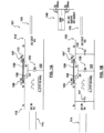
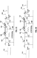
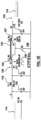
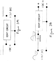
- FIG. 1A-1E shown are exemplary embodiments of an electronic direct voltage transformer circuit illustrated generally by reference numerals 101-105 according to alternate embodiments.
- the electronic direct voltage transformer circuit 101 comprises an input node 110, an output node 112 and a magnetic storage unit 100 coupled electrically between the input node 110 and the output node 112 connected to a load.
- the input node 110 is located at the source side for receiving an input DC (direct voltage) power source having an input supply voltage 114.
- the magnetic storage unit 100 then serves to transform or transfer power from the source side to the load using high frequency magnetic energy storage or charged from the load and discharged to the source when the load voltage is higher than the equivalent voltage transfer dictated by the transfer constant Kv.
- Magnetic storage unit 100 comprises a common core 130 having one or more sets of windings (e.g.
- the magnetic storage unit 100 further comprises two or more switches (e.g. a first switch 108 and a second switch 109).
- the first and second switches 108-109 are AC bidirectional switches, illustrated generally at 140, that are switched on, alternately, that is opposite to one another and have a switching frequency in a kilohertz range.
- the first set of windings 106 and second set of windings 107 are magnetically coupled together by common core 130.
- the second set of windings 107 is located in series aiding or series opposing connection with the first set of windings 106 within a common magnetic path.
- the first switch 108 is directly connected to the first set of windings 106 (and can be located on either side of first set of windings 106 as illustrated in the difference between FIGS. 1A and 1C ).
- the second switch 109 is connected between the two set of windings 106, 107 and the common ground.
- the output node 112 is then connected to the second set of windings 107 such that the output node provides an output DC power, and an output DC voltage 116. Further the amplitude or magnitude of the output voltage 116 is based on one or more of: a winding ratio between first and second sets of windings 106,107, a polarity of the first and second set of windings 106, 107 and the duty cycle of the switching frequency of the first and second switches 108, 109.
- the magnetic storage unit 100 is configured to receive the input power and transfer it to the output node 112 such that the first and second set of windings 106, 107 provide magnetic storage of energy in a continuous fashion therein even while the first and second switches 108 and 109 are being alternately and in an opposing manner being switched on and off.
- the switch 108 and 109 duty cycle is set at a predefined number the set of windings 106, 107 are coupled together and each have a predefined number of windings.
- Nd refers to the number of windings to produce the inductance Ld of second set of windings 107
- Nc refers to the additional turns to produce the inductance Lc (referring to the combination of the first and second set of windings 106, 107). That is, Nc+Nd produces the inductance Lc+Ld.
- the inductance is proportional to the number of turns squared.
- the following describes the general mode of operation of the magnetic storage unit referred to in each of Figures 1A-1E .
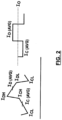
- the first mode of operation when the first switch 108 is switched on (and second switch 109 is switched off), the line current flows through the first and second sets of windings 106, 107 (storage node 113) to the load at output node 112.
- the output current Io is equivalent to the input current Is which is equivalent to the current flowing through the set of windings Ic and Id.
- the current flowing through the sets of windings 106, 107 supports the load current (Io) plus the magnetic charging current.
- the combination of both sets of windings 106, 107 (storage node 113) preferably supports the desired peak output current Io plus the peak charging current and the current flowing through the second set of windings 107 similarly must support the peak limits of the discharge current. That is, the magnetic energy flux (known as BH) load of the common core 130 of storage node 113 preferably does not reach saturation with the peak ampere-turns mentioned above.
- BH magnetic energy flux
- the input supply voltage 114 is preferably a DC waveform
- the output voltage 116 at output node 112 is also a DC waveform
- the switching frequency of switches within the magnetic storage unit 100 is in the kilohertz range (e.g. 20kHz). That is, as will be described, the magnetic storage unit 100, facilitates transforming a power DCvoltage input to a power DCvoltage output at the load by transforming or transferring the input energy using magnetic energy storage as the transfer medium.
- Kv is a predefined constant that is dependent on the turns ratio between the first and second sets of windings 106, 107 (e.g. specifically on the number of turns Nc of the first set of windings 106 relative to the number of turns Nd of the second set of windings 107). That is, K v is a function of the turns constant K i and the charge/ discharge ratio K x as defined below.
- the charge/discharge ratio is dependent upon delta-tc, the time to switch from the first switch 108 being switched on to the second switch 109 being switched on and delta-td which is the discharge time when the second switch 109 is on (first switch 108 is off).
- a constant duty cycle will yield a constant output voltage 116 relative to the input voltage 114 and thereby transform an inputDC waveform to an outputDC waveform.
- the first switch 108 is switched off and the second switch 107 is switched on, now all the current flows through the second set of windings 107 only, and the current instantly increases from Ich to Idh to maintain the conservation of energy in the magnetic field. That is, the current magnitude increases by the turns ratio difference.
- Nc of set of windings 106 is equivalent to Nd of set of windings 107 then the current flowing through the second set of windings 107 increases to Idh (e.g. doubles in value compared to the current just before switch 108 is turned off in this case).
- the current through the storage node 113 slowly decreases from Idh to Idl, the relation being shown above. Further, the current instantly decreases at the end of the discharge time interval when the second switch 109 is turned off and the first switch 108 is turned back on, from Idl to Icl.
- the input sine wave shape e.g. input supply voltage 114
- the input sine wave shape of voltage 114 is converted at the fixed transfer ratio (e.g. determined as mentioned earlier by the Kv constant) to
- the current ripple magnitude in the storage element 113 is a function of V s , the inductance values and the duty cycle.
- ⁇ I c ⁇ I d K i
- I c ( avg ) ,I d ( avg ) are a function of the load current, duty cycle and the number of turns of the storage set of windings.
- an electronic direct voltage transformer 102, 103 according to alternate embodiments where an input capacitor 117 located between the first switch 108 and/or the first set of windings 106 and the common ground.
- the input capacitor 117 is configured for cooperating with both the first and second sets of windings 106, 107 to suppress the high frequency current components in the kilohertz range from the input supply side of the EDVT circuit 102, 103 respectively.
- an output capacitor 118 located between the second set of windings 107 and the common ground (e.g.
- the output capacitor 118 configured for cooperating with the first and second sets of windings 106, 107 to suppress the high frequency components in the kilohertz range (e.g. generated by the high frequency switching rate of the first and second switches 108, 109) of the output power/voltage at the output node.
- an input inductor 119 located between the input node and the first switch 108 and a filtering capacitor 120 located between the input node and the common ground.
- the input inductor 119 cooperating with the input capacitor 120 to provide additional suppression of high frequency components from the input signal (e.g. 114) provided to the magnetic storage unit 100.
- Figure 1E provides some exemplary values for the components to filter the appropriate frequencies in a line frequency embodiment.
- the input and output powers, voltages and currents have no harmonic content below the switching frequency , including the absence of the kilohertz high frequency component.
- the first and second switches 108, 109) are operated at only certain portions of input waveform of the input supply voltage 114 such that only a portion of the input voltage 114 waveform is transferred to the load as output voltage 116.
- the output can be a power source (e.g. 114) and can be a DC voltage and the switches 108, 109 duty cycles are modulated at regular repeating variations so as to produce varying output voltages 116 which are selected from linear sinusoid voltages or non-linear output voltages to the input 114.
- DC power can be transferred to an alternating voltage (AC) power line.
- AC alternating voltage
- ripple currents are not affected by the load current Io. That is, when the load is disconnected such as to cause a zero load current, there will only be the ripple current component above and below zero at the high frequency.
- the output voltage 116 will still be defined by the ratio to the input voltage 114 defined above.
- a feedback circuit can be used to monitor output waveform 116 that is used to alter the duty cycle of the switches 108,109 to provide a more stable output voltage with respect to the input voltage or provide a more stable input voltage when charged from the load and discharged to the source when the load voltage is higher than the equivalent voltage transfer dictated by the transfer constant Kv.
- the present invention provides improved flexibility for the electronic direct voltage transformer circuits by allowing electronic timing switching controls of the output voltage provided to a load and allowing an DC input power to be supplied as an output DC power or in reverse when charged from the load and discharged to the source when the load voltage is higher than the equivalent voltage transfer dictated by the transfer constant Kv such that the amplitude is dependent upon the turns ratio between the sets of windings and the duty cycle of the switches used in the magnetic storage unit 100 described herein. Therefore there is material saving, cost and increased flexibility.
- the electronics variable nature of the transformer circuit 101-105 allows control of output voltage, power and current without any mechanical wear items and at increased efficiencies.
Landscapes
- Engineering & Computer Science (AREA)
- Power Engineering (AREA)
- Dc-Dc Converters (AREA)
- Details Of Television Scanning (AREA)
Claims (19)
- Un circuit de transformateur électronique de tension en courant continu, CC, comprenant :un noeud d'entrée (110) adapté pour recevoir une puissance CC d'entrée depuis une source de puissance à tension en courant continu ;une unité de couplage de stockage magnétique (100) comprenant :un premier ensemble d'enroulements (106) couplé à un premier commutateur CA bidirectionnel (108), le premier commutateur CA bidirectionnel (108) étant configuré pour recevoir un courant de charge d'entrée associé à une tension d'entrée (114) ;un deuxième ensemble d'enroulements (107) électriquement en série avec le premier ensemble d'enroulements (106), les premier et deuxième ensembles d'enroulements (106, 107) étant configurés pour partager un noyau commun (130) ; un deuxième commutateur CA bidirectionnel (109) connecté avec une extrémité directement entre les premier et deuxième ensembles d'enroulements (106, 107) et avec une autre extrémité à une terre commune, les premier et deuxième commutateurs CA bidirectionnels (108, 109) étant configurés pour avoir une fréquence de commutation dans la plage du kilohertz et pour commuter entre activé et désactivé dans des modes alternatifs ; etun noeud de sortie (112) connecté au deuxième ensemble d'enroulements (107), le noeud de sortie (112) étant adapté pour fournir une puissance CC de sortie, l'puissance CC de sortie étant adaptée pour avoir une tension de sortie Vo (116) avec une amplitude sur la base de la tension d'entrée (114) Vs , où Vo = KvVs et Kv est une constante de transfert prédéfinie qui est proportionnelle à un cycle de service D des premier et deuxièmes commutateurs CA bidirectionnels (108, 109),de sorte que
 dans lequel l'unité de couplage de stockage magnétique (100) est configurée pour transférer une puissance CC de la source de puissance à tension en courant continu au noeud de sortie (112) au moyen d'un couplage de stockage magnétique fourni par les premier et deuxième ensembles d'enroulements (106, 107) de façon à recevoir une puissance CC d'entrée et transférer une tension en courant continu en tant que puissance CC d'entrée du noeud d'entrée (110) au noeud de sortie (112) en fournissant la puissance CC de sortie de sorte que le premier ensemble d'enroulements (106) et le deuxième ensemble d'enroulements (107) sont configurés pour fournir un stockage magnétique d'énergie sur la base de chacun des premier (108) et deuxième (109) commutateur CA bidirectionnel étant configuré de façon à être commuté en continu ;
dans lequel, lorsqu'une charge de sortie est zéro, la tension de sortie est configurée pour rester proportionnelle à la tension d'entrée par ledit Vo = KvVs. - Le circuit selon la revendication 1, dans lequel le noeud d'entrée (110) est configuré pour être la source de puissance et la charge de sortie est configurée pour être un absorbeur de puissance.
- Le circuit selon la revendication 2 comprenant en outre un condensateur (118) situé entre le deuxième ensemble d'enroulements (107) et la terre commune, le condensateur (118) étant configuré pour supprimer des composants à fréquence élevée dans la plage du kilohertz de la tension de sortie au niveau du noeud de sortie (112).
- Le circuit selon la revendication 2, dans lequel la tension de sortie (116) est en outre configurée pour être dépendante d'un rapport de tours du premier ensemble d'enroulements (106) au deuxième ensemble d'enroulements (107) de sorte que la variation d'au moins un parmi le rapport de tours et le cycle de service fait varier directement l'amplitude de signal de tension de sortie.
- Le circuit selon la revendication 2 étant configuré pour fournir un rapport constant prédéfini de la tension de sortie à la tension d'entrée du noeud d'entrée (110) au noeud de sortie (112), indépendamment de la forme d'onde d'entrée, une forme d'onde d'entrée étant convertie au rapport de transfert prédéfini en charge de sortie.
- Le circuit selon la revendication 2 étant en outre configuré pour fournir une distorsion harmonique de puissance proche de zéro à la fois dans la puissance CC d'entrée et la puissance CC de sortie avec un cycle de service fixe.
- Le circuit selon la revendication 2 étant en outre configuré pour fournir une correction harmonique pour des charges de sortie non linéaires lorsque le cycle de service est configuré pour être modulé de façon incrémentielle de façon à corriger des fluctuations anticipées desdites charges de sortie non linéaires.
- Le circuit selon la revendication 3 comprenant en outre un deuxième condensateur (117) situé entre le premier commutateur bidirectionnel (108) et la terre commune, le deuxième condensateur (117) étant configuré pour supprimer les composantes de courant à haute fréquence au niveau du noeud d'entrée (110).
- Le circuit selon la revendication 8 comprenant en outre un inducteur d'entrée (119) situé entre le noeud d'entrée (110) et le premier commutateur CA bidirectionnel (108) et un condensateur d'entrée (120) situé entre le noeud d'entrée (110) et la terre commune, l'inducteur d'entrée (119) étant configuré pour coopérer avec le condensateur d'entrée (120) pour fournir une suppression supplémentaire des composantes à haute fréquence au niveau du noeud d'entrée (110).
- Le circuit selon la revendication 9 dans lequel la puissance CC d'entrée et la puissance CC de sortie sont configurées pour avoir un contenu harmonique limité autre qu'un contenu de fréquence de l'ordre du hertz de puissance de base et une composante de haute fréquence de l'ordre du kilohertz générée par la fréquence de commutation a un contenu de fréquence limité.
- Le circuit selon la revendication 2, dans lequel, pendant une première durée où le premier commutateur CA bidirectionnel (108) est configuré pour être activé et le deuxième commutateur CA bidirectionnel (109) est configuré pour être désactivé ; un courant peut circuler depuis les premier et deuxième ensembles d'enroulements (106, 107) vers la charge de sortie, les premier et deuxième ensembles d'enroulements (106, 107) étant configurés pour être chargés magnétiquement pendant la première durée durant laquelle le premier commutateur CA bidirectionnel (108) est fermé.
- Le circuit selon la revendication 11, dans lequel, pendant une deuxième durée où le deuxième commutateur CA bidirectionnel (109) est activé et le premier commutateur CA bidirectionnel (108) est désactivé, le courant est configuré pour arrêter de circuler au niveau du premier ensemble d'enroulements (106) et le courant au niveau de la charge de sortie est maintenu par le deuxième ensemble d'enroulements (107) lorsqu'il se décharge magnétiquement.
- Le circuit selon la revendication 12, dans lequel l'unité de couplage de stockage magnétique (100) est configurée pour maintenir un rapport constant de la tension de sortie à la tension d'entrée (114) pour la charge de sortie pendant l'opération de commutation des premier et deuxième commutateurs CA bidirectionnels (108, 109).
- Le circuit selon la revendication 13, dans lequel la tension de sortie (116) est configurée pour être modulée proportionnellement sur la base d'au moins l'un parmi un rapport de tours du premier ensemble d'enroulements (106) au deuxième ensemble d'enroulements (107) et le cycle de service.
- Le circuit selon la revendication 2 étant configuré de sorte que les premier et deuxièmes commutateurs CA bidirectionnels (108, 109) sont actionnés à seulement certaines durées d'une forme d'onde de tension d'entrée de sorte que seulement une partie de la forme d'onde de tension d'entrée est à la charge de sortie.
- Le circuit selon la revendication 2 dans lequel la puissance CC d'entrée est configurée pour être basée sur une tension CC et les cycles de service des premier et deuxième commutateurs CA bidirectionnels (108, 109) sont modulés à des fréquences de l'ordre du hertz régulièrement répétées avec des variations de cycle de service.
- Le circuit selon la revendication 2 étant configuré pour utiliser une rétroaction pour contrôler le cycle de service des premier et deuxième commutateurs CA bidirectionnels (108, 109) pour fournir une sortie plus stable vis-à-vis des variations de la tension d'entrée (114) ou inversement lors de la charge depuis la charge de sortie et de la décharge vers la source de puissance à tension en courant continu lorsque la tension de charge de sortie est supérieure à un transfert de tension équivalent dépendant de la constante de transfert prédéfinie Kv.
- Le circuit selon la revendication 2 dans lequel la puissance est configurée pour circuler depuis un côté de charge vers un côté d'entrée lorsque la tension de charge de sortie est supérieure à une tension transformée régie par la constante de transfert prédéfinie Kv.
- Le circuit selon la revendication 2 dans lequel la puissance est configurée pour circuler depuis un côté charge vers un côté d'entrée lorsque la tension de charge de sortie est supérieure à une tension transformée régie par la constante de transfert prédéfinie Kv et la tension d'entrée est une tension en courant continu.
Applications Claiming Priority (2)
| Application Number | Priority Date | Filing Date | Title |
|---|---|---|---|
| US201462054063P | 2014-09-23 | 2014-09-23 | |
| PCT/CA2015/000494 WO2016044915A1 (fr) | 2014-09-23 | 2015-09-18 | Transformateur de tension continue électronique |
Publications (3)
| Publication Number | Publication Date |
|---|---|
| EP3198712A1 EP3198712A1 (fr) | 2017-08-02 |
| EP3198712A4 EP3198712A4 (fr) | 2018-04-25 |
| EP3198712B1 true EP3198712B1 (fr) | 2023-10-18 |
Family
ID=55579981
Family Applications (1)
| Application Number | Title | Priority Date | Filing Date |
|---|---|---|---|
| EP15843123.9A Active EP3198712B1 (fr) | 2014-09-23 | 2015-09-18 | Transformateur de tension continue électronique |
Country Status (6)
| Country | Link |
|---|---|
| US (1) | US10096423B2 (fr) |
| EP (1) | EP3198712B1 (fr) |
| JP (1) | JP6789929B2 (fr) |
| CA (1) | CA2962079C (fr) |
| ES (1) | ES2967266T3 (fr) |
| WO (1) | WO2016044915A1 (fr) |
Citations (2)
| Publication number | Priority date | Publication date | Assignee | Title |
|---|---|---|---|---|
| US20020185993A1 (en) * | 2001-06-07 | 2002-12-12 | Philips Electronics North America Corporation. | Active clamp step-down converter with power switch voltage clamping function |
| EP2662970A2 (fr) * | 2012-05-09 | 2013-11-13 | Steca Elektronik GmbH | Agencement de circuit |
Family Cites Families (25)
| Publication number | Priority date | Publication date | Assignee | Title |
|---|---|---|---|---|
| US4504896A (en) * | 1981-03-18 | 1985-03-12 | Rca Corporation | Switching dc-to-dc converters |
| US4577268A (en) * | 1982-12-20 | 1986-03-18 | Rca Corporation | Switching dc-to-dc converters |
| US5321348A (en) * | 1991-03-08 | 1994-06-14 | Vlt Corporation | Boost switching power conversion |
| US5432431A (en) * | 1992-05-21 | 1995-07-11 | Vlt Corporation | Boost switching power conversion using saturable inductors |
| US5747972A (en) * | 1995-01-11 | 1998-05-05 | Microplanet Ltd. | Method and apparatus for electronic power control |
| US6442047B1 (en) * | 1999-10-08 | 2002-08-27 | Lambda Electronics, Inc. | Power conversion apparatus and methods with reduced current and voltage switching |
| US6400579B2 (en) * | 2000-03-24 | 2002-06-04 | Slobodan Cuk | Lossless switching DC to DC converter with DC transformer |
| US6784644B2 (en) * | 2001-02-22 | 2004-08-31 | Virginia Tech Intellectual Properties, Inc. | Multiphase clamp coupled-buck converter and magnetic integration |
| US6798670B2 (en) * | 2001-04-02 | 2004-09-28 | International Rectifier Corporation | DC-DC converter |
| US6975098B2 (en) * | 2002-01-31 | 2005-12-13 | Vlt, Inc. | Factorized power architecture with point of load sine amplitude converters |
| US6822427B2 (en) * | 2002-05-01 | 2004-11-23 | Technical Witts, Inc. | Circuits and circuit elements for high efficiency power conversion |
| US6771518B2 (en) * | 2002-08-26 | 2004-08-03 | Potentia Semiconductor, Inc. | DC converters |
| US6714426B1 (en) * | 2002-11-04 | 2004-03-30 | Semtech Corporation | Multiple-phase, multi-module power supply system for high frequency operation |
| US8324872B2 (en) * | 2004-03-26 | 2012-12-04 | Marvell World Trade, Ltd. | Voltage regulator with coupled inductors having high coefficient of coupling |
| US7161331B2 (en) * | 2005-04-11 | 2007-01-09 | Yuan Ze University | Boost converter utilizing bi-directional magnetic energy transfer of coupling inductor |
| JP4692154B2 (ja) * | 2005-08-25 | 2011-06-01 | サンケン電気株式会社 | Dc/dcコンバータ |
| JP2007209061A (ja) * | 2006-01-31 | 2007-08-16 | Mitsumi Electric Co Ltd | 電源装置 |
| US7382113B2 (en) * | 2006-03-17 | 2008-06-03 | Yuan Ze University | High-efficiency high-voltage difference ratio bi-directional converter |
| JP5191042B2 (ja) * | 2008-04-16 | 2013-04-24 | サンケン電気株式会社 | 双方向dc−dcコンバータ |
| JP2012124974A (ja) * | 2009-04-02 | 2012-06-28 | Mitsubishi Electric Corp | Dc/dcコンバータ |
| US8803361B2 (en) * | 2011-01-19 | 2014-08-12 | Schneider Electric It Corporation | Apparatus and method for providing uninterruptible power |
| US8773085B2 (en) * | 2011-03-22 | 2014-07-08 | Ledillion Technologies Inc. | Apparatus and method for efficient DC-to-DC conversion through wide voltage swings |
| WO2012128768A1 (fr) * | 2011-03-24 | 2012-09-27 | Polar Semiconductor, Inc. | Alimentation électrique sans pont et à commutateur en série |
| JP5934000B2 (ja) * | 2012-03-16 | 2016-06-15 | サンケン電気株式会社 | 双方向dc−dcコンバータ |
| US9059634B2 (en) * | 2013-03-22 | 2015-06-16 | Vito Rinaldi | Electronic sine wave transformer |
-
2015
- 2015-09-18 EP EP15843123.9A patent/EP3198712B1/fr active Active
- 2015-09-18 JP JP2017515775A patent/JP6789929B2/ja active Active
- 2015-09-18 WO PCT/CA2015/000494 patent/WO2016044915A1/fr not_active Ceased
- 2015-09-18 CA CA2962079A patent/CA2962079C/fr active Active
- 2015-09-18 ES ES15843123T patent/ES2967266T3/es active Active
-
2017
- 2017-03-23 US US15/466,938 patent/US10096423B2/en active Active
Patent Citations (2)
| Publication number | Priority date | Publication date | Assignee | Title |
|---|---|---|---|---|
| US20020185993A1 (en) * | 2001-06-07 | 2002-12-12 | Philips Electronics North America Corporation. | Active clamp step-down converter with power switch voltage clamping function |
| EP2662970A2 (fr) * | 2012-05-09 | 2013-11-13 | Steca Elektronik GmbH | Agencement de circuit |
Also Published As
| Publication number | Publication date |
|---|---|
| ES2967266T3 (es) | 2024-04-29 |
| CA2962079C (fr) | 2021-11-02 |
| US10096423B2 (en) | 2018-10-09 |
| JP6789929B2 (ja) | 2020-11-25 |
| US20170194093A1 (en) | 2017-07-06 |
| EP3198712A1 (fr) | 2017-08-02 |
| CA2962079A1 (fr) | 2016-03-31 |
| EP3198712A4 (fr) | 2018-04-25 |
| WO2016044915A1 (fr) | 2016-03-31 |
| JP2017529824A (ja) | 2017-10-05 |
Similar Documents
| Publication | Publication Date | Title |
|---|---|---|
| CN101626197B (zh) | 功率因数校正的效率改进 | |
| US7830686B2 (en) | Isolated high power bi-directional DC-DC converter | |
| US8466662B2 (en) | Power transfer between independent power ports utilizing a single transformer | |
| EP2487783A2 (fr) | Onduleur de puissance et amplificateur de puissance à commutation à ultra-haute efficacité | |
| JPH0586147B2 (fr) | ||
| JP5552149B2 (ja) | コンバータ及び双方向コンバータ | |
| EP2156542A2 (fr) | Modèle prédictif pour un convertisseur de puissance à commutation par paliers et topologie d'onduleur inductif | |
| CN102664528A (zh) | 一种开关电源 | |
| EP2976831B1 (fr) | Transformateur électronique d'ondes sinusoïdales | |
| JP5130542B2 (ja) | 降圧型スイッチングdc/dcコンバータ | |
| JP2014239579A (ja) | Dc/dcコンバータおよびバッテリ充放電装置 | |
| US8675375B2 (en) | System and method for input voltage transient response control | |
| JP6482009B2 (ja) | 多入力コンバータ及び双方向コンバータ | |
| US5771168A (en) | Power factor correction apparatus | |
| JP5535290B2 (ja) | 双方向コンバータ | |
| EP3198712B1 (fr) | Transformateur de tension continue électronique | |
| US11881777B2 (en) | DC pulse power supply device | |
| EP1844539B1 (fr) | Procede et convertisseur pour convertir une tension en courant continu en une sortie de courant alternatif a trois phases | |
| JP6347389B2 (ja) | 非接触給電装置、非接触受電装置、及び非接触給電システム | |
| RU177680U1 (ru) | Многофункциональный импульсный преобразователь | |
| RU2558808C2 (ru) | Вентильный выпрямитель для дуговой сварки |
Legal Events
| Date | Code | Title | Description |
|---|---|---|---|
| STAA | Information on the status of an ep patent application or granted ep patent |
Free format text: STATUS: THE INTERNATIONAL PUBLICATION HAS BEEN MADE |
|
| PUAI | Public reference made under article 153(3) epc to a published international application that has entered the european phase |
Free format text: ORIGINAL CODE: 0009012 |
|
| STAA | Information on the status of an ep patent application or granted ep patent |
Free format text: STATUS: REQUEST FOR EXAMINATION WAS MADE |
|
| 17P | Request for examination filed |
Effective date: 20170411 |
|
| AK | Designated contracting states |
Kind code of ref document: A1 Designated state(s): AL AT BE BG CH CY CZ DE DK EE ES FI FR GB GR HR HU IE IS IT LI LT LU LV MC MK MT NL NO PL PT RO RS SE SI SK SM TR |
|
| AX | Request for extension of the european patent |
Extension state: BA ME |
|
| DAV | Request for validation of the european patent (deleted) | ||
| DAX | Request for extension of the european patent (deleted) | ||
| A4 | Supplementary search report drawn up and despatched |
Effective date: 20180322 |
|
| RIC1 | Information provided on ipc code assigned before grant |
Ipc: H02M 1/088 20060101ALI20180316BHEP Ipc: H02M 3/158 20060101AFI20180316BHEP |
|
| STAA | Information on the status of an ep patent application or granted ep patent |
Free format text: STATUS: EXAMINATION IS IN PROGRESS |
|
| 17Q | First examination report despatched |
Effective date: 20200124 |
|
| REG | Reference to a national code |
Ref country code: DE Ref legal event code: R079 Free format text: PREVIOUS MAIN CLASS: H02M0003158000 Ipc: H02M0001120000 Ref country code: DE Ref legal event code: R079 Ref document number: 602015086160 Country of ref document: DE Free format text: PREVIOUS MAIN CLASS: H02M0003158000 Ipc: H02M0001120000 |
|
| GRAP | Despatch of communication of intention to grant a patent |
Free format text: ORIGINAL CODE: EPIDOSNIGR1 |
|
| STAA | Information on the status of an ep patent application or granted ep patent |
Free format text: STATUS: GRANT OF PATENT IS INTENDED |
|
| RIC1 | Information provided on ipc code assigned before grant |
Ipc: H02M 3/158 20060101ALI20230320BHEP Ipc: H02M 1/12 20060101AFI20230320BHEP |
|
| INTG | Intention to grant announced |
Effective date: 20230412 |
|
| GRAS | Grant fee paid |
Free format text: ORIGINAL CODE: EPIDOSNIGR3 |
|
| GRAA | (expected) grant |
Free format text: ORIGINAL CODE: 0009210 |
|
| STAA | Information on the status of an ep patent application or granted ep patent |
Free format text: STATUS: THE PATENT HAS BEEN GRANTED |
|
| RAP3 | Party data changed (applicant data changed or rights of an application transferred) |
Owner name: RINALDI, VITO |
|
| RIN1 | Information on inventor provided before grant (corrected) |
Inventor name: RINALDI, VITO |
|
| AK | Designated contracting states |
Kind code of ref document: B1 Designated state(s): AL AT BE BG CH CY CZ DE DK EE ES FI FR GB GR HR HU IE IS IT LI LT LU LV MC MK MT NL NO PL PT RO RS SE SI SK SM TR |
|
| REG | Reference to a national code |
Ref country code: GB Ref legal event code: FG4D |
|
| REG | Reference to a national code |
Ref country code: CH Ref legal event code: EP |
|
| REG | Reference to a national code |
Ref country code: DE Ref legal event code: R096 Ref document number: 602015086160 Country of ref document: DE |
|
| REG | Reference to a national code |
Ref country code: IE Ref legal event code: FG4D |
|
| REG | Reference to a national code |
Ref country code: LT Ref legal event code: MG9D |
|
| REG | Reference to a national code |
Ref country code: NL Ref legal event code: MP Effective date: 20231018 |
|
| REG | Reference to a national code |
Ref country code: AT Ref legal event code: MK05 Ref document number: 1623353 Country of ref document: AT Kind code of ref document: T Effective date: 20231018 |
|
| PG25 | Lapsed in a contracting state [announced via postgrant information from national office to epo] |
Ref country code: NL Free format text: LAPSE BECAUSE OF FAILURE TO SUBMIT A TRANSLATION OF THE DESCRIPTION OR TO PAY THE FEE WITHIN THE PRESCRIBED TIME-LIMIT Effective date: 20231018 |
|
| PG25 | Lapsed in a contracting state [announced via postgrant information from national office to epo] |
Ref country code: GR Free format text: LAPSE BECAUSE OF FAILURE TO SUBMIT A TRANSLATION OF THE DESCRIPTION OR TO PAY THE FEE WITHIN THE PRESCRIBED TIME-LIMIT Effective date: 20240119 |
|
| PG25 | Lapsed in a contracting state [announced via postgrant information from national office to epo] |
Ref country code: IS Free format text: LAPSE BECAUSE OF FAILURE TO SUBMIT A TRANSLATION OF THE DESCRIPTION OR TO PAY THE FEE WITHIN THE PRESCRIBED TIME-LIMIT Effective date: 20240218 |
|
| PG25 | Lapsed in a contracting state [announced via postgrant information from national office to epo] |
Ref country code: LT Free format text: LAPSE BECAUSE OF FAILURE TO SUBMIT A TRANSLATION OF THE DESCRIPTION OR TO PAY THE FEE WITHIN THE PRESCRIBED TIME-LIMIT Effective date: 20231018 |
|
| PG25 | Lapsed in a contracting state [announced via postgrant information from national office to epo] |
Ref country code: AT Free format text: LAPSE BECAUSE OF FAILURE TO SUBMIT A TRANSLATION OF THE DESCRIPTION OR TO PAY THE FEE WITHIN THE PRESCRIBED TIME-LIMIT Effective date: 20231018 |
|
| REG | Reference to a national code |
Ref country code: ES Ref legal event code: FG2A Ref document number: 2967266 Country of ref document: ES Kind code of ref document: T3 Effective date: 20240429 |
|
| PG25 | Lapsed in a contracting state [announced via postgrant information from national office to epo] |
Ref country code: LT Free format text: LAPSE BECAUSE OF FAILURE TO SUBMIT A TRANSLATION OF THE DESCRIPTION OR TO PAY THE FEE WITHIN THE PRESCRIBED TIME-LIMIT Effective date: 20231018 Ref country code: IS Free format text: LAPSE BECAUSE OF FAILURE TO SUBMIT A TRANSLATION OF THE DESCRIPTION OR TO PAY THE FEE WITHIN THE PRESCRIBED TIME-LIMIT Effective date: 20240218 Ref country code: GR Free format text: LAPSE BECAUSE OF FAILURE TO SUBMIT A TRANSLATION OF THE DESCRIPTION OR TO PAY THE FEE WITHIN THE PRESCRIBED TIME-LIMIT Effective date: 20240119 Ref country code: BG Free format text: LAPSE BECAUSE OF FAILURE TO SUBMIT A TRANSLATION OF THE DESCRIPTION OR TO PAY THE FEE WITHIN THE PRESCRIBED TIME-LIMIT Effective date: 20240118 Ref country code: AT Free format text: LAPSE BECAUSE OF FAILURE TO SUBMIT A TRANSLATION OF THE DESCRIPTION OR TO PAY THE FEE WITHIN THE PRESCRIBED TIME-LIMIT Effective date: 20231018 Ref country code: PT Free format text: LAPSE BECAUSE OF FAILURE TO SUBMIT A TRANSLATION OF THE DESCRIPTION OR TO PAY THE FEE WITHIN THE PRESCRIBED TIME-LIMIT Effective date: 20240219 |
|
| PG25 | Lapsed in a contracting state [announced via postgrant information from national office to epo] |
Ref country code: SE Free format text: LAPSE BECAUSE OF FAILURE TO SUBMIT A TRANSLATION OF THE DESCRIPTION OR TO PAY THE FEE WITHIN THE PRESCRIBED TIME-LIMIT Effective date: 20231018 Ref country code: RS Free format text: LAPSE BECAUSE OF FAILURE TO SUBMIT A TRANSLATION OF THE DESCRIPTION OR TO PAY THE FEE WITHIN THE PRESCRIBED TIME-LIMIT Effective date: 20231018 Ref country code: PL Free format text: LAPSE BECAUSE OF FAILURE TO SUBMIT A TRANSLATION OF THE DESCRIPTION OR TO PAY THE FEE WITHIN THE PRESCRIBED TIME-LIMIT Effective date: 20231018 Ref country code: NO Free format text: LAPSE BECAUSE OF FAILURE TO SUBMIT A TRANSLATION OF THE DESCRIPTION OR TO PAY THE FEE WITHIN THE PRESCRIBED TIME-LIMIT Effective date: 20240118 Ref country code: LV Free format text: LAPSE BECAUSE OF FAILURE TO SUBMIT A TRANSLATION OF THE DESCRIPTION OR TO PAY THE FEE WITHIN THE PRESCRIBED TIME-LIMIT Effective date: 20231018 Ref country code: HR Free format text: LAPSE BECAUSE OF FAILURE TO SUBMIT A TRANSLATION OF THE DESCRIPTION OR TO PAY THE FEE WITHIN THE PRESCRIBED TIME-LIMIT Effective date: 20231018 |
|
| PG25 | Lapsed in a contracting state [announced via postgrant information from national office to epo] |
Ref country code: DK Free format text: LAPSE BECAUSE OF FAILURE TO SUBMIT A TRANSLATION OF THE DESCRIPTION OR TO PAY THE FEE WITHIN THE PRESCRIBED TIME-LIMIT Effective date: 20231018 |
|
| REG | Reference to a national code |
Ref country code: DE Ref legal event code: R097 Ref document number: 602015086160 Country of ref document: DE |
|
| PG25 | Lapsed in a contracting state [announced via postgrant information from national office to epo] |
Ref country code: CZ Free format text: LAPSE BECAUSE OF FAILURE TO SUBMIT A TRANSLATION OF THE DESCRIPTION OR TO PAY THE FEE WITHIN THE PRESCRIBED TIME-LIMIT Effective date: 20231018 |
|
| PG25 | Lapsed in a contracting state [announced via postgrant information from national office to epo] |
Ref country code: SK Free format text: LAPSE BECAUSE OF FAILURE TO SUBMIT A TRANSLATION OF THE DESCRIPTION OR TO PAY THE FEE WITHIN THE PRESCRIBED TIME-LIMIT Effective date: 20231018 |
|
| PG25 | Lapsed in a contracting state [announced via postgrant information from national office to epo] |
Ref country code: SM Free format text: LAPSE BECAUSE OF FAILURE TO SUBMIT A TRANSLATION OF THE DESCRIPTION OR TO PAY THE FEE WITHIN THE PRESCRIBED TIME-LIMIT Effective date: 20231018 Ref country code: SK Free format text: LAPSE BECAUSE OF FAILURE TO SUBMIT A TRANSLATION OF THE DESCRIPTION OR TO PAY THE FEE WITHIN THE PRESCRIBED TIME-LIMIT Effective date: 20231018 Ref country code: RO Free format text: LAPSE BECAUSE OF FAILURE TO SUBMIT A TRANSLATION OF THE DESCRIPTION OR TO PAY THE FEE WITHIN THE PRESCRIBED TIME-LIMIT Effective date: 20231018 Ref country code: EE Free format text: LAPSE BECAUSE OF FAILURE TO SUBMIT A TRANSLATION OF THE DESCRIPTION OR TO PAY THE FEE WITHIN THE PRESCRIBED TIME-LIMIT Effective date: 20231018 Ref country code: DK Free format text: LAPSE BECAUSE OF FAILURE TO SUBMIT A TRANSLATION OF THE DESCRIPTION OR TO PAY THE FEE WITHIN THE PRESCRIBED TIME-LIMIT Effective date: 20231018 Ref country code: CZ Free format text: LAPSE BECAUSE OF FAILURE TO SUBMIT A TRANSLATION OF THE DESCRIPTION OR TO PAY THE FEE WITHIN THE PRESCRIBED TIME-LIMIT Effective date: 20231018 |
|
| PLBE | No opposition filed within time limit |
Free format text: ORIGINAL CODE: 0009261 |
|
| STAA | Information on the status of an ep patent application or granted ep patent |
Free format text: STATUS: NO OPPOSITION FILED WITHIN TIME LIMIT |
|
| 26N | No opposition filed |
Effective date: 20240719 |
|
| PG25 | Lapsed in a contracting state [announced via postgrant information from national office to epo] |
Ref country code: SI Free format text: LAPSE BECAUSE OF FAILURE TO SUBMIT A TRANSLATION OF THE DESCRIPTION OR TO PAY THE FEE WITHIN THE PRESCRIBED TIME-LIMIT Effective date: 20231018 |
|
| PG25 | Lapsed in a contracting state [announced via postgrant information from national office to epo] |
Ref country code: SI Free format text: LAPSE BECAUSE OF FAILURE TO SUBMIT A TRANSLATION OF THE DESCRIPTION OR TO PAY THE FEE WITHIN THE PRESCRIBED TIME-LIMIT Effective date: 20231018 |
|
| PG25 | Lapsed in a contracting state [announced via postgrant information from national office to epo] |
Ref country code: MC Free format text: LAPSE BECAUSE OF FAILURE TO SUBMIT A TRANSLATION OF THE DESCRIPTION OR TO PAY THE FEE WITHIN THE PRESCRIBED TIME-LIMIT Effective date: 20231018 |
|
| REG | Reference to a national code |
Ref country code: CH Ref legal event code: PL |
|
| PG25 | Lapsed in a contracting state [announced via postgrant information from national office to epo] |
Ref country code: LU Free format text: LAPSE BECAUSE OF NON-PAYMENT OF DUE FEES Effective date: 20240918 |
|
| REG | Reference to a national code |
Ref country code: BE Ref legal event code: MM Effective date: 20240930 |
|
| PG25 | Lapsed in a contracting state [announced via postgrant information from national office to epo] |
Ref country code: BE Free format text: LAPSE BECAUSE OF NON-PAYMENT OF DUE FEES Effective date: 20240930 |
|
| PG25 | Lapsed in a contracting state [announced via postgrant information from national office to epo] |
Ref country code: CH Free format text: LAPSE BECAUSE OF NON-PAYMENT OF DUE FEES Effective date: 20240930 |
|
| PG25 | Lapsed in a contracting state [announced via postgrant information from national office to epo] |
Ref country code: IE Free format text: LAPSE BECAUSE OF NON-PAYMENT OF DUE FEES Effective date: 20240918 |
|
| PG25 | Lapsed in a contracting state [announced via postgrant information from national office to epo] |
Ref country code: FI Free format text: LAPSE BECAUSE OF FAILURE TO SUBMIT A TRANSLATION OF THE DESCRIPTION OR TO PAY THE FEE WITHIN THE PRESCRIBED TIME-LIMIT Effective date: 20231019 |
|
| PGFP | Annual fee paid to national office [announced via postgrant information from national office to epo] |
Ref country code: DE Payment date: 20250813 Year of fee payment: 11 |
|
| PGFP | Annual fee paid to national office [announced via postgrant information from national office to epo] |
Ref country code: IT Payment date: 20250825 Year of fee payment: 11 |
|
| PGFP | Annual fee paid to national office [announced via postgrant information from national office to epo] |
Ref country code: GB Payment date: 20250814 Year of fee payment: 11 |
|
| PGFP | Annual fee paid to national office [announced via postgrant information from national office to epo] |
Ref country code: FR Payment date: 20250808 Year of fee payment: 11 |
|
| PG25 | Lapsed in a contracting state [announced via postgrant information from national office to epo] |
Ref country code: CY Free format text: LAPSE BECAUSE OF FAILURE TO SUBMIT A TRANSLATION OF THE DESCRIPTION OR TO PAY THE FEE WITHIN THE PRESCRIBED TIME-LIMIT; INVALID AB INITIO Effective date: 20150918 |
|
| PGFP | Annual fee paid to national office [announced via postgrant information from national office to epo] |
Ref country code: ES Payment date: 20251017 Year of fee payment: 11 |
|
| PG25 | Lapsed in a contracting state [announced via postgrant information from national office to epo] |
Ref country code: HU Free format text: LAPSE BECAUSE OF FAILURE TO SUBMIT A TRANSLATION OF THE DESCRIPTION OR TO PAY THE FEE WITHIN THE PRESCRIBED TIME-LIMIT; INVALID AB INITIO Effective date: 20150918 |