EP3199662A1 - Cible de pulvérisation cathodique et procédé de fabrication de celle-ci - Google Patents
Cible de pulvérisation cathodique et procédé de fabrication de celle-ci Download PDFInfo
- Publication number
- EP3199662A1 EP3199662A1 EP15845101.3A EP15845101A EP3199662A1 EP 3199662 A1 EP3199662 A1 EP 3199662A1 EP 15845101 A EP15845101 A EP 15845101A EP 3199662 A1 EP3199662 A1 EP 3199662A1
- Authority
- EP
- European Patent Office
- Prior art keywords
- phase
- sputtering target
- phases
- alloy
- raw material
- Prior art date
- Legal status (The legal status is an assumption and is not a legal conclusion. Google has not performed a legal analysis and makes no representation as to the accuracy of the status listed.)
- Withdrawn
Links
Images



Classifications
-
- C—CHEMISTRY; METALLURGY
- C23—COATING METALLIC MATERIAL; COATING MATERIAL WITH METALLIC MATERIAL; CHEMICAL SURFACE TREATMENT; DIFFUSION TREATMENT OF METALLIC MATERIAL; COATING BY VACUUM EVAPORATION, BY SPUTTERING, BY ION IMPLANTATION OR BY CHEMICAL VAPOUR DEPOSITION, IN GENERAL; INHIBITING CORROSION OF METALLIC MATERIAL OR INCRUSTATION IN GENERAL
- C23C—COATING METALLIC MATERIAL; COATING MATERIAL WITH METALLIC MATERIAL; SURFACE TREATMENT OF METALLIC MATERIAL BY DIFFUSION INTO THE SURFACE, BY CHEMICAL CONVERSION OR SUBSTITUTION; COATING BY VACUUM EVAPORATION, BY SPUTTERING, BY ION IMPLANTATION OR BY CHEMICAL VAPOUR DEPOSITION, IN GENERAL
- C23C14/00—Coating by vacuum evaporation, by sputtering or by ion implantation of the coating forming material
- C23C14/22—Coating by vacuum evaporation, by sputtering or by ion implantation of the coating forming material characterised by the process of coating
- C23C14/34—Sputtering
- C23C14/3407—Cathode assembly for sputtering apparatus, e.g. Target
- C23C14/3414—Metallurgical or chemical aspects of target preparation, e.g. casting, powder metallurgy
-
- B—PERFORMING OPERATIONS; TRANSPORTING
- B22—CASTING; POWDER METALLURGY
- B22F—WORKING METALLIC POWDER; MANUFACTURE OF ARTICLES FROM METALLIC POWDER; MAKING METALLIC POWDER; APPARATUS OR DEVICES SPECIALLY ADAPTED FOR METALLIC POWDER
- B22F1/00—Metallic powder; Treatment of metallic powder, e.g. to facilitate working or to improve properties
- B22F1/09—Mixtures of metallic powders
-
- B—PERFORMING OPERATIONS; TRANSPORTING
- B22—CASTING; POWDER METALLURGY
- B22F—WORKING METALLIC POWDER; MANUFACTURE OF ARTICLES FROM METALLIC POWDER; MAKING METALLIC POWDER; APPARATUS OR DEVICES SPECIALLY ADAPTED FOR METALLIC POWDER
- B22F3/00—Manufacture of workpieces or articles from metallic powder characterised by the manner of compacting or sintering; Apparatus specially adapted therefor ; Presses and furnaces
- B22F3/10—Sintering only
- B22F3/1003—Use of special medium during sintering, e.g. sintering aid
- B22F3/1007—Atmosphere
-
- B—PERFORMING OPERATIONS; TRANSPORTING
- B22—CASTING; POWDER METALLURGY
- B22F—WORKING METALLIC POWDER; MANUFACTURE OF ARTICLES FROM METALLIC POWDER; MAKING METALLIC POWDER; APPARATUS OR DEVICES SPECIALLY ADAPTED FOR METALLIC POWDER
- B22F9/00—Making metallic powder or suspensions thereof
- B22F9/02—Making metallic powder or suspensions thereof using physical processes
- B22F9/06—Making metallic powder or suspensions thereof using physical processes starting from liquid material
- B22F9/08—Making metallic powder or suspensions thereof using physical processes starting from liquid material by casting, e.g. through sieves or in water, by atomising or spraying
- B22F9/082—Making metallic powder or suspensions thereof using physical processes starting from liquid material by casting, e.g. through sieves or in water, by atomising or spraying atomising using a fluid
-
- C—CHEMISTRY; METALLURGY
- C22—METALLURGY; FERROUS OR NON-FERROUS ALLOYS; TREATMENT OF ALLOYS OR NON-FERROUS METALS
- C22C—ALLOYS
- C22C28/00—Alloys based on a metal not provided for in groups C22C5/00 - C22C27/00
-
- C—CHEMISTRY; METALLURGY
- C22—METALLURGY; FERROUS OR NON-FERROUS ALLOYS; TREATMENT OF ALLOYS OR NON-FERROUS METALS
- C22C—ALLOYS
- C22C9/00—Alloys based on copper
-
- C—CHEMISTRY; METALLURGY
- C23—COATING METALLIC MATERIAL; COATING MATERIAL WITH METALLIC MATERIAL; CHEMICAL SURFACE TREATMENT; DIFFUSION TREATMENT OF METALLIC MATERIAL; COATING BY VACUUM EVAPORATION, BY SPUTTERING, BY ION IMPLANTATION OR BY CHEMICAL VAPOUR DEPOSITION, IN GENERAL; INHIBITING CORROSION OF METALLIC MATERIAL OR INCRUSTATION IN GENERAL
- C23C—COATING METALLIC MATERIAL; COATING MATERIAL WITH METALLIC MATERIAL; SURFACE TREATMENT OF METALLIC MATERIAL BY DIFFUSION INTO THE SURFACE, BY CHEMICAL CONVERSION OR SUBSTITUTION; COATING BY VACUUM EVAPORATION, BY SPUTTERING, BY ION IMPLANTATION OR BY CHEMICAL VAPOUR DEPOSITION, IN GENERAL
- C23C14/00—Coating by vacuum evaporation, by sputtering or by ion implantation of the coating forming material
- C23C14/06—Coating by vacuum evaporation, by sputtering or by ion implantation of the coating forming material characterised by the coating material
- C23C14/0623—Sulfides, selenides or tellurides
-
- C—CHEMISTRY; METALLURGY
- C23—COATING METALLIC MATERIAL; COATING MATERIAL WITH METALLIC MATERIAL; CHEMICAL SURFACE TREATMENT; DIFFUSION TREATMENT OF METALLIC MATERIAL; COATING BY VACUUM EVAPORATION, BY SPUTTERING, BY ION IMPLANTATION OR BY CHEMICAL VAPOUR DEPOSITION, IN GENERAL; INHIBITING CORROSION OF METALLIC MATERIAL OR INCRUSTATION IN GENERAL
- C23C—COATING METALLIC MATERIAL; COATING MATERIAL WITH METALLIC MATERIAL; SURFACE TREATMENT OF METALLIC MATERIAL BY DIFFUSION INTO THE SURFACE, BY CHEMICAL CONVERSION OR SUBSTITUTION; COATING BY VACUUM EVAPORATION, BY SPUTTERING, BY ION IMPLANTATION OR BY CHEMICAL VAPOUR DEPOSITION, IN GENERAL
- C23C14/00—Coating by vacuum evaporation, by sputtering or by ion implantation of the coating forming material
- C23C14/06—Coating by vacuum evaporation, by sputtering or by ion implantation of the coating forming material characterised by the coating material
- C23C14/14—Metallic material, boron or silicon
-
- H—ELECTRICITY
- H01—ELECTRIC ELEMENTS
- H01J—ELECTRIC DISCHARGE TUBES OR DISCHARGE LAMPS
- H01J37/00—Discharge tubes with provision for introducing objects or material to be exposed to the discharge, e.g. for the purpose of examination or processing thereof
- H01J37/32—Gas-filled discharge tubes
- H01J37/34—Gas-filled discharge tubes operating with cathodic sputtering
- H01J37/3411—Constructional aspects of the reactor
- H01J37/3414—Targets
- H01J37/3426—Material
-
- B—PERFORMING OPERATIONS; TRANSPORTING
- B22—CASTING; POWDER METALLURGY
- B22F—WORKING METALLIC POWDER; MANUFACTURE OF ARTICLES FROM METALLIC POWDER; MAKING METALLIC POWDER; APPARATUS OR DEVICES SPECIALLY ADAPTED FOR METALLIC POWDER
- B22F2201/00—Treatment under specific atmosphere
- B22F2201/01—Reducing atmosphere
-
- B—PERFORMING OPERATIONS; TRANSPORTING
- B22—CASTING; POWDER METALLURGY
- B22F—WORKING METALLIC POWDER; MANUFACTURE OF ARTICLES FROM METALLIC POWDER; MAKING METALLIC POWDER; APPARATUS OR DEVICES SPECIALLY ADAPTED FOR METALLIC POWDER
- B22F2301/00—Metallic composition of the powder or its coating
- B22F2301/10—Copper
-
- B—PERFORMING OPERATIONS; TRANSPORTING
- B22—CASTING; POWDER METALLURGY
- B22F—WORKING METALLIC POWDER; MANUFACTURE OF ARTICLES FROM METALLIC POWDER; MAKING METALLIC POWDER; APPARATUS OR DEVICES SPECIALLY ADAPTED FOR METALLIC POWDER
- B22F2998/00—Supplementary information concerning processes or compositions relating to powder metallurgy
- B22F2998/10—Processes characterised by the sequence of their steps
-
- B—PERFORMING OPERATIONS; TRANSPORTING
- B22—CASTING; POWDER METALLURGY
- B22F—WORKING METALLIC POWDER; MANUFACTURE OF ARTICLES FROM METALLIC POWDER; MAKING METALLIC POWDER; APPARATUS OR DEVICES SPECIALLY ADAPTED FOR METALLIC POWDER
- B22F2999/00—Aspects linked to processes or compositions used in powder metallurgy
Definitions
- the present invention relates to a sputtering target, which is used in the formation of a Cu-In-Ga-Se compound film (hereinafter, abbreviated as the CIGS film, occasionally) for forming the light-absorbing layer of the CIGS thin-film solar cell, and a method of producing the sputtering target.
- a sputtering target which is used in the formation of a Cu-In-Ga-Se compound film (hereinafter, abbreviated as the CIGS film, occasionally) for forming the light-absorbing layer of the CIGS thin-film solar cell, and a method of producing the sputtering target.
- This thin-film solar cell using the compound semiconductor film has a basic structure, in which a Mo electrode layer, which becomes the plus electrode, is formed on a soda-lime glass substrate; a light-absorbing layer made of the CIGS film is formed on the Mo electrode layer; a buffer layer, which is made of ZnS, CdS, or the like, is formed on the light-absorbing layer; and a transparent electrode layer, which becomes the minus electrode, is formed on the buffer layer.
- a sputtering method which is suitable for deposition on the substrate with large area.
- the selenization method is adopted.
- an In film is sputtering-deposited by using an In sputtering target.
- a binary Cu-Ga alloy film is sputtering-deposited on the In film by using a binary Cu-Ga alloy sputtering target.
- the CIGS film is formed by heat treating the obtained laminated precursor film, which is made of the In film and the binary Cu-Ga alloy film, in an Se atmosphere.
- the order of forming the In film and the binary Cu-Ga alloy film is interchangeable.
- the Cu-Ln-Ga-Se compound film is formed by: sputter-depositing the Cu-Ga alloy in the thickness of about 500 nm; forming the laminated film, in which the Ln film having the thickness of about 500 nm is sputtered on the film; by heating the laminated film at 500°C in H 2 Se gas; and by having Se diffuse into the Cu-Ga-In.
- the Cu-Ga alloy sputtering target is essential for this selenization method for the CIGS solar cell using the light-absorbing layer of the Cu-In-Ga-Se compound film (CIGS film) to be produced.
- the band gap changes depending on the ratio between In and Ga for the light absorption wavelength to change in the chalcopyrite-based CIGS film.
- the light absorption wavelength shifts to the low wavelength side when the Ga ratio is high.
- the thin-film solar cell with a Cu-Ga-Se 2 compound film free of In is highly expected on application as the top cell in the tandem structure of the CIGS thin-film solar cell. Therefore, there is demand for a Cu-Ga alloy sputtering target containing Ga at high concentration in order to deposit the Cu-Ga-Se 2 compound film.
- Patent Literature 2 Patent Literature 2
- Patent Literature 3 Patent Literature 3
- a sputtering target which is made of Cu-Ga alloy including multiple phases; and includes 40 weight% or more and 60 weight% or less of Ga and the Cu balance containing inevitable impurities, is disclosed in PTL 2.
- the multiple phases include a segregation phase containing 80 weight% or more of Ga.
- a Cu-Ga alloy sputtering target which is constituted from a Cu-Ga alloy material with the average composition of: 32 weight% or more and 45 weight% or less of Ga; the balance Cu; inevitable impurities; and inevitable pores, is disclosed in PTL 3.
- the Cu-Ga alloy phase including 65 weight% or more of gallium includes at least one phase among the ⁇ 1 phase; the ⁇ 2 phase; and the ⁇ 3 phase.
- the Cu-Ga alloy of the Cu-Ga alloy sputtering target disclosed in PTL 2 is produced by rapidly solidifying the melted raw material after melting the raw material.
- the Cu-Ga alloy (including ⁇ 3 phase and ⁇ phase), which includes the segregation phase containing 80 weight% or more of Ga, is produced by passing through the steps of: melting the mixture, which is made of 40 weight% or more and 60 weight% or less of Ga and the Cu balance containing inevitable impurities, by heating in the melting furnace; cooling the melted mixture to 254°C for the ⁇ 3 phase of the Cu-Ga alloy to be solidified and formed in the melted mixture; and then, heat treating the water-cooled mold or crucible at a temperature of 200°C or more and less than 254°C after the temperature in the step of cooling reached to 245°C for the ⁇ phase of the Cu-Ga alloy to be precipitated between the ⁇ 3 phases.
- the Cu-Ga alloy sputtering target disclosed in PTL 2 has a technical problem described below. Ga is contained in high concentration and the segregation phase including 80 weight% or more of Ga having poor workability exists in the Cu-Ga alloy sputtering target disclosed in PTL 2. Thus, cracking originated from the segregation phase is likely to occur during machining the sputtering target. In addition, there is the same technical problem in the sputtering target in which alkaline metal such as Na and the like is added to the Cu-Ga alloy.
- the Cu-Ga alloy material in which the ratio of the volume of the region including copper at less than 47 weight% to the entire volume of the Cu-Ga alloy material is 2% or less, is proposed in order to reduce the segregation phase as described in PTL 2 or the like.
- the part excluding the region including copper at less than 47 weight% becomes the region including gallium at 32 weight% to 53 weight% or less.
- the ⁇ phase which shows brittleness when the gallium content is 32 weight% or more, becomes the main phase.
- the present invention is made under the circumstances described above.
- the purpose of the present invention is to provide a Cu-Ga alloy sputtering target, which is unlikely to be cracked during machining even if it includes Ga at a high concentration, and a method of producing the Cu-Ga alloy sputtering target.
- the present invention includes the following aspects in order to solve the above-described problems.
- the sputtering target of the present invention coarsening of the crystal grains of the ⁇ phase can be suppressed; and occurrence of cracking during machining the target can be reduced, in the Cu-Ga alloy sintered material, since the sintered material, which has the component composition including: 30.0-67.0 atomic% of Ga; and the Cu balance containing inevitable impurities, has the structure in which ⁇ phases made of Cu-Ga alloy are dispersed in the matrix of ⁇ phases made of Cu-Ga alloy.
- the average grain size of the ⁇ phases is 5.0-50.0 ⁇ m. More preferably, the ratio of the intensity of the main peak among diffraction peaks attributed to the ⁇ phases to the intensity of the main peak among diffraction peaks attributed to the ⁇ phases (0 phase intensity/ ⁇ phase intensity) is 0.01-10.0. Diffraction peaks attributed to the ⁇ phases and the ⁇ phases are obtained from the X-ray diffraction (XRD) patterns.
- the Cu-Ga alloy sputtering target of the aspect of the present invention including high concentration Ga, cracking is unlikely to occur; and the yield in the target production can be improved.
- the high Ga concentration-containing light-absorbing layer of the CIGS thin-film solar cell can be deposited; and the usage of the sputtering target can contribute to improvement of the photoelectric conversion efficiency in the light-absorbing layer.
- solar cells having high power generation efficiency can be produced.
- the sputtering target of the present embodiment has a component composition including: 30.0-67.0 atomic% of Ga; and the Cu balance containing inevitable impurities.
- the sputtering target is a sintered material having a structure in which ⁇ phases made of Cu-Ga alloy are dispersed in a matrix of the ⁇ phases made of Cu-Ga alloy.
- the structure in which ⁇ phases made of Cu-Ga alloy are dispersed in a matrix of the ⁇ phases made of Cu-Ga alloy means that ⁇ phases and ⁇ phases precipitated during sintering coexist in the sintered material; it is in the state where one phase of the ⁇ phase and the ⁇ phase surrounds the other phase; and it is in the state where each phase is dispersed without being agglomerated on the macro level.
- the reason for setting the Ga content to the range of 30.0-67.0 atomic% in the present embodiment is that if the Ga content were less than 30.0 atomic%, the ⁇ phase would almost disappear. In this case, the structure practically becomes a single phase of the ⁇ phase; and the workability of the target deteriorates drastically. On the other hand, if the Ga content exceeded 67.0 atomic%, the pure Ga (melting point is 29.6°C) would be formed even though the ⁇ phase is present. In this case, melting out of Ga occurs by heat in cutting work of the target; and cracking of the target occurs originated from the melted-out Ga.
- the ⁇ phase in the present embodiment includes ⁇ and ⁇ 1- ⁇ 3 in the phase diagram shown in FIG. 1 .
- the structure of the sputtering target is explained in reference to FIGS. 2 and 3 by taking the sputtering target of the present embodiment, which is the sputtering target made of the Cu-Ga alloy sintered material, for the representative example.
- the sputtering target made of the Cu-Ga alloy sintered material was obtained by hot press sintering the atomized powder made of the Cu-Ga alloy having the Ga content of 50.0 atomic% by retaining the powder under the pressure of 50 MPa at the sintering temperature of 165°C for 2 hours, while the Ar gas flew at 10 L/min.
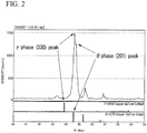
- FIG. 2 is an X-ray diffraction (XRD) pattern obtained by performing the analysis by the X-ray diffraction (XRD) on the above-described sputtering target.
- FIG. 3 is a photograph of the compositional image (COMPO image) obtained by performing the electron probe micro analysis (EPMA) on the above-described sputtering target.
- XRD X-ray diffraction
- EPMA electron probe micro analysis
- both of the diffraction peak attributed to the ⁇ phases of the Cu-Ga alloy (Cu 9 Ga 4 phase) and the diffraction peak attributed to the ⁇ phase of the Cu-Ga alloy (CuGa 2 phase) were observed in the above-described sputtering target.
- the ratio of the intensity of the main peak among diffraction peaks attributed to the ⁇ phases to the intensity of the main peak among diffraction peaks attributed to the ⁇ phases ( ⁇ phase intensity/ ⁇ phase intensity, referred as " ⁇ phase ratio", occasionally) was 0.80.
- the two phases to the ⁇ phase and the 0 phase exist in the state where they were dispersed each other in the sputtering target.
- the whitest part indicates the region having a relatively high Ga content in the photograph of the COMPO image shown in FIG. 3 .
- the light gray area and the dark gray area indicate the ⁇ phase and the ⁇ phase, respectively.
- the above-described sputtering target had the crystal structure in which the ⁇ phases with a relatively high Ga content exist in the matrix of the ⁇ phases. Even in the case where Na or K was added to the sputtering target, the crystal structure of the sputtering target had the two-phase-coexisting structure of the ⁇ phase and the ⁇ phase.
- the reason for the two phases of the ⁇ phase and the ⁇ phase to coexist in the crystal structure of the sputtering target is that the ratio of the intensity of the main peak among diffraction peaks attributed to the ⁇ phases to the intensity of the main peak among diffraction peaks attributed to the ⁇ phases, both of which are obtained from the X-ray diffraction (XRD) pattern of the raw material Cu-Ga alloy powder, is 0.01 to 10.0.
- the ⁇ phase in the raw material Cu-Ga alloy powder is low, specifically in the case where the ⁇ phase ratio is 0.5 or less, by setting the sintering temperature at 254°C or more, the liquid phase of the ⁇ phase appears from the Cu-Ga alloy powder during sintering.
- the sintering target made of the sintered material with a high density can be obtained even in the powder sintering by the low temperature hot pressing.
- the ⁇ phases precipitate around 254°C.
- the liquid phase does not precipitate form the ⁇ phase.
- the ⁇ phases in the raw material Cu-Ga alloy are retained. If the sintering temperature were set to 254°C or more in this setup instead, it would become hard to retain the shape of the sintered material since too much liquid phase is formed from the ⁇ phase.
- the ⁇ phase ratio exceeds 0.5
- the component composition of the mixed raw material powder includes 30.0-42.6 atomic% of Ga and the Cu balance containing inevitable impurities, Ga diffuses from the Cu-Ga alloy raw material powder made of the ⁇ phase to the Cu-Ga alloy raw material powder made of the ⁇ phase.
- the precipitation of the liquid phase of Ga can be suppressed; and the sintered material can be obtained even in sintering at 254C or more.
- mixing ratio of the Cu-Ga alloy material powder, in which the ⁇ phase ratio exceeds 0.5 is 30% or less. If the mixing ratio exceeded 30%, it would be hard to retain the shape of the sintered material due to the excessive amount of the liquid phase from the ⁇ phase even if Ga diffuses from the Cu-Ga alloy raw material powder made of the ⁇ phase to the Cu-Ga alloy raw material powder made of the ⁇ phase.
- the advantage of the two phases of the ⁇ phase and the ⁇ phase being coexisting is that coarsening of the crystal grains of the ⁇ phase is suppressed by the existence of the ⁇ phase; and it becomes hard for the sputtering target to be cracked during machining of the sputtering target by miniaturization of the average crystal grain size in the target structure.
- the Cu-Ga alloy sputtering target was obtained by hot press sintering the atomized powder made of the Cu-Ga alloy having the Ga content of 33.0 atomic% by retaining the powder under the pressure of 60 MPa at the sintering temperature of 700°C for 2 hours, while the Ar gas flew at 10 L/min.
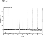
- the obtained sputtering target was subjected to the analysis by the X-ray diffraction (XRD). The measurement results are shown on the XRD pattern in FIG. 4 .
- the electron probe micro analysis was performed on the sputtering target and the obtained photograph of the compositional image (COMPO image) is shown in FIG. 5 .
- the XRD pattern in FIG. 4 only the diffraction peaks attributed to the ⁇ phases of the Cu-Ga alloy are observed.
- the entire image is in gray; and there is almost no parches of dark and light gray spots.
- the black spots in the image are pores. Because of these, it is demonstrated that the main phase of the matrix is formed from the single phase of the ⁇ phase; and there is no ⁇ phase including relatively high content of Ga, in sintered material of this sputtering target based on this comparative example.
- the average crystal grain size of the ⁇ phases is 5.0-50.0 ⁇ m; the average crystal grain size of the ⁇ phase is 5.0-100.0 ⁇ m; and the ratio of the intensity of the main peak among diffraction peaks attributed to the ⁇ phases to the intensity of the main peak among diffraction peaks attributed to the ⁇ phases (0 phase intensity/ ⁇ phase intensity), both of which are obtained from the X-ray diffraction (XRD) pattern, is in the range of 0.01-10.0, in the sputtering target of the present embodiment.
- the average crystal grain size of the ⁇ phases exceeds 50.0 ⁇ m and the average crystal grain size of the ⁇ phase exceeds 100.0 ⁇ m in the sputtering target of the present embodiment, chipping (cracking, fracturing, and the like) is likely to occur during machining after sputtering target production.
- the ⁇ phase ratio which expresses that the ⁇ phase and the ⁇ phase coexist in the sputtering target, is set in the range of 0.01-10.0, coarsening of the ⁇ phases is suppressed by the existence of the ⁇ phase.
- the sputtering target is unlikely to be cracked during machining of the sputtering target.
- 0.05-15 atomic % of Na may be included in the sputtering target in order to improve the photoelectric conversion efficiency since the sputtering target of the present embodiment can be utilized for formation of the CIGS film, which becomes the light-absorbing layer of the solar cell.
- the Na may be included at least in one form of Na compounds of sodium fluoride, sodium sulfide, and sodium selenide.
- 0.05-15 atomic% of K may be included in the sputtering target instead of Na; and the K may be included at least in one form of K compounds of potassium fluoride, potassium chloride, potassium bromide, potassium iodide, potassium sulfide, potassium selenide, and potassium niobate.
- Na and K may be included at the same time. In this case, the total of Na and K is set to 0.05-15 atomic%.
- the method of producing the sputtering target of the present embodiment is a method for producing the sputtering target of the present embodiment.
- the method includes the step of producing a sintered material by sintering a powder, which is a Cu-Ga alloy powder including 40.0-67.0 atomic% of Ga and the Cu balance containing inevitable impurities; and a ratio of an intensity of a main peak among diffraction peaks attributed to ⁇ phases to an intensity of a main peak among diffraction peaks attributed to ⁇ phases ( ⁇ phase intensity/ ⁇ phase intensity), both of which are obtained from an X-ray diffraction (XRD) pattern, is 0.01-10.0, in non-oxidizing atmosphere or reducing atmosphere: at a sintering temperature of 254°C or more and 450°C or less in a case where the ratio of main peaks is 0.5 or less; or at a sintering temperature lower than 254°C in a case where the ratio of main peaks is more than 0.5.
- Adjustment of the crystal grain size in the sintered material is made easier by using the Cu-Ga alloy powder in the method of producing the sputtering target.
- the structure, in which the ⁇ phases of the Cu-Ga alloy are dispersed in the matrix of the ⁇ phases of the Cu-Ga alloy, is obtained in the sintered material; and the average crystal grain size of the ⁇ phases is set to 50.0 ⁇ m or less, because: the ratio of the intensity of the main peak among diffraction peaks attributed to ⁇ phases to the intensity of the main peak among diffraction peaks attributed to ⁇ phases ( ⁇ phase intensity/ ⁇ phase intensity), both of which are obtained from an X-ray diffraction (XRD) pattern, is 0.01-10.0; and the sintering temperature for obtaining the sintered material related to the sputtering target is set in the range of 150-450°C.
- the other method of producing the sputtering target of the present embodiment is a method for producing the above-described sputtering target.
- the structure, in which the ⁇ phases of the Cu-Ga alloy are dispersed in the matrix of the ⁇ phases of the Cu-Ga alloy, is obtained; and the average crystal grain size of the ⁇ phases is set to 50.0 ⁇ m or less, even in the composition containing 30.0-42.6 atomic% of Ga in the sintered material.
- the procedure for producing the Cu-Ga binary sputtering target of the present embodiment includes the steps of: producing the raw material powder by the gas atomizing method after weighting Cu metal cramps and Ga metal cramps in predetermined amounts as alloy powders and melting each of them in a crucible; mixing the raw material powders and if necessary the Na compound raw material powder and the K compound material powder in non-oxidizing atmosphere; sintering the raw material powder at a low temperature in non-oxidizing atmosphere or reducing atmosphere; and cutting the surface of the sintered material obtained in the step of sintering.
- a carbon crucible is filled with each of Cu metal cramps and Ga metal cramps in predetermined composition ratios; and the Cu-Ga alloy atomized powder, which is the raw material powder, is prepared by the gas atomized method by Ar gas.
- the non-oxidizing atmosphere is atmosphere free of oxygen, such as Ar atmosphere, vacuum atmosphere, and the like.
- the reducing atmosphere is atmosphere including reducing gas such as H 2 , CO, and the like.
- the sputtering target having the diameter of 50 mm and the thickness of 6 mm is produced by machining the surface part and outer periphery part of the obtained sintered material on a lathe.
- the sputtering target after machining is bonded on the backing plate made of Cu, sus (stainless), or other metal (for example, Mo) by using In as solder to be used in sputtering.
- the entire target is sealed in vacuum packing or inert gas replacement packing in order to avoid oxidation and moisture absorption.
- the sputtering target produced as described above is installed on the DC magnetron sputtering apparatus using Ar gas as sputter gas.
- a pulse DC power supply applying pulse voltage or a DC power supply without pulse can be used.
- the ⁇ phases are dispersed in the matrix of the ⁇ phases of the sintered material of Cu-Ga alloy in the present embodiment.
- the reason why the two phases of the ⁇ phase and the ⁇ phase coexist is that the ratio of the intensity of the main peak among diffraction peaks attributed to 8 phases to the intensity of the main peak among diffraction peaks attributed to ⁇ phases ( ⁇ phase intensity/ ⁇ phase intensity), both of which are obtained from an X-ray diffraction (XRD) pattern, is 0.01-10.0.
- the ⁇ phase in the raw material Cu-Ga alloy powder is low, specifically in the case where the ⁇ phase ratio is 0.5 or less, by setting the sintering temperature at 254°C or more, the liquid phase of the ⁇ phase appears from the Cu-Ga alloy powder during sintering.
- sintering becomes so called the liquid phase sintering; and the sintered material is densified easily. Therefore, the sintered material with a high density can be obtained even in the powder sintering by the low temperature hot pressing.
- the ⁇ phases precipitate around 254°C.
- the ⁇ phase in the raw material Cu-Ga alloy powder is high, specifically, in the case where the ⁇ phase ratio exceeds 0.5, by setting the sintering temperature at less than 254°C, the liquid phase does not precipitate form the ⁇ phase. Thus, the ⁇ phases in the raw material Cu-Ga alloy are retained. If the sintering temperature were set to 254°C or more in this setup instead, it would become hard to retain the shape of the sintered material since too much liquid phase is formed from the ⁇ phase. Based on the phase diagram of the Cu-Ga alloy in " Binary Alloy Phase Diagrams (2nd. Editi on)", it is foreseen that the phase separation occurs certainly in the case where the atomic ratio of Ga is 42.6% or more.
- the advantage of the two phases being coexisting is that coarsening of the crystal grains of the ⁇ phases is suppressed by the existence of the ⁇ phase; and the average grain size in the target structure becomes small, making it hard for the sputtering target to be cracked during machining of the sputtering target.
- the Cu metal cramps and the Ga metal cramps both of which had the purity of 4N grade (purity: 99.99%), were prepared. They were weighted for the total weight to be 1200g with the component compositions shown in Table 1.
- the raw material powder A and the raw material powder B were prepared by the gas atomizing method by Ar gas. These raw material powders were sieved through 125 ⁇ m to be classified.
- the gas atomizing condition was: 1000-1200°C of the temperature in melting; 28kgf/cm 2 of the ejection gas pressure; and 1.5 mm of the nozzle diameter.
- the mixing conditions by the rocking mixer were: 72 rpm of the rotation speed; and 30 minutes of the mixing time.
- the raw material powders were obtained: by weighting the raw material powder A and the Na additives shown in Table 2 in the mixing ratios of the raw material powder A and the Na additives shown in Table 1 and 2, respectively; and then by them by a rocking mixer.
- the raw material powders were obtained: by weighting the raw material powders A and B in the mixing ratios shown in Table 1; by mixing them by the rocking mixer to obtain the mixture; by adding the Na additives shown in Table 2 to the mixture in the mixing ratios shown in Table 2; and then by mixing them by the rocking mixer.
- the Na additives the Na compound powders having the purity of 3N (purity: 99.9%) were used.
- the raw material powder were obtained: by weighting the raw material powders A and the K additives shown in Table 2 in the mixing ratios of the raw material powder A and the K additives shown in Table 1 and 2, respectively; and by mixing them by the rocking mixer.
- Example 17 the raw material powder was obtained: by weighting the raw material powder A, the raw material powder B, and the K additive in the mixing ratios of the raw material powders A, B, and the K additive shown in Table 1 and 2, respectively; and then by mixing them by the rocking mixer.
- Example 18 the raw material powder was obtained: by weighting the raw material powder A, the Na and K additives shown in Table 2 in the mixing ratios of the raw material powder A and the Na and K additives shown in Table 1 and 2, respectively; and then by mixing them by the rocking mixer.
- Example 14 was a representative example in the case where the K compound was added instead of the Na compound.
- the raw material powder in Example 14 was obtained by mixing the Cu-Ga raw material powder obtained in advance and the K compound in the mixing ratio shown in Table 2 in mixing by the rocking mixer.
- the Na compound (NaF) and the K compound (KCl) were prepared and mixed with the Cu-Ga raw material powder obtained in advance.
- Comparative Example 1 the Ga content in the raw material powder A was less compared to the case in Examples of the present invention; and the ⁇ phase ratio was low. In addition, hot pressing was performed at a high temperature beyond the temperature range in the method of producing the sputtering target of the present invention. In Comparative Example 2, the Ga content in the raw material powder A was excessive compared to the case in Examples of the present invention; and the ⁇ phase was absent. In Comparative Example 3, although the raw material powders A and B were used, the mixing ratio of the raw material powder B was excessive; and the Ga content in the Cu-Ga alloy raw material powder was less compared to the case in Examples of the present invention. In Comparative Example 4, although the raw material powders A and B were used, the mixing ratio of the raw material powder A was excessive.
- Hot pressing Ar 160 1 1 55 Ex. 6
- Hot pressing Ar 160 2 60
- HIP Vacuum 340 1 45 Ex. 9
- Hot pressing Vacuum 160 1 60
- 10 HIP Vacuum 350 3 60
- Hot pressing Vacuum 340 2 30
- 12 Hot pressing Vacuum 350 2 35
- Hot pressing Vacuum 340 2 35
- 14 Hot pressing Vacuum 160 2 60
- Hot pressing Ar 160 2 55 Ex. 16
- Hot pressing Ar 450 2 50
- Hot pressing Vacuum 160 3 60
- Hot pressing Ar 160 2 55
- Hot pressing Ar 160 1 60
- Hot pressing Vacuum 150 2 60
- Hot pressing Ar 160 1.5 55
- Hot pressing Vacuum 165 2 60 C.
- Hot pressing Ar 700 2 60 C.
- Hot pressing Vacuum 380 I 60 C.
- Hot pressing Vacuum 400 1 60
- the sample surfaces cut out from the sputtering targets were polished to mirror surface, and subjected to etching by the etching solution made of nitric acid and pure water.
- five compositional images (COMPO images) were taken in the magnification range of 50-1000 times, in which the crystal grain boundaries were distinguished in EPMA.
- obtained images were converted to binary images by converting the taken images to black and white images by using a commercially available image processing software such as WinRoof (manufactured by Mitani Co.) and the like, and using a threshold value.
- the maximum circumcircles were drawn on arbitrary selected 20 crystal grains of the ⁇ phase (or the ⁇ phase) in the image obtained by showing the ⁇ phase (or the ⁇ phase) in black.
- the average of the diameter in the image was defined as the average crystal grain size in the image.
- the average value of the averages from five images was defined as the average crystal grain size.
- the XRD patterns were measured after wet-polishing the sputter surfaces of the sputtering targets by the SiC-Paper (grit 180) and drying.
- the apparatus and measurement conditions used in this analysis are shown below.
- the ⁇ phase ratio was obtained from the intensities of the ⁇ phase (102) plane and the ⁇ phase (330) plane in the diffraction peak graph (for example, FIG. 2 ) obtained in the above-described conditions. Specifically, the ⁇ phase ratio was obtained from the intensity ratio by using the formula shown below.
- ⁇ phase ratio I obs ⁇ phase / I obs ⁇ phase I obs ( ⁇ phase) was the measure peak intensity of the ⁇ phase (102) plane and I obs ( ⁇ phase) was the measure peak intensity of the ⁇ phase (330) plane.
- the produced sputtering targets were machined on a lathe. Then, existence or non-existence of chipping (cracking or fracturing) was measured. In addition, the target surface roughness (Ra: arithmetic average roughness) after machining was measured.
- the conditions for machining on the lathe were that: 100 rpm of the rotation speed; 0.7 mm of the depth of cut; and 0.097 mm/rev of the feed.
- the insert commercially available inserts made of cemented carbide material were used.
- the target surface roughness (Ra: arithmetic average roughness) after machining was measured by the surface roughness measuring instrument (Model: Surf Test SV-3000H4, manufactured by Mitsutoyo Co. Ltd.) after machining the produced sputtering targets on a lathe.
- the surface roughness measuring instrument Model: Surf Test SV-3000H4, manufactured by Mitsutoyo Co. Ltd.
- measurement was performed using a needle with the stylus tip radius curvature of 2 ⁇ m and the stylus tip angle of 60° on a straight line orthogonal to the processing mark lines according to JIS B 0651:2001
- Comparative Example 1 which was the case where the raw material powder A was the raw material powder, the Ga component was less; and hot pressing was performed in an excessively high temperature deviated from the temperature range in the method of producing the sputtering target of the present invention. Therefore, the ⁇ phase was not formed; the structure of the target became the single phase of the ⁇ phase; and chipping occurred in cutting.
- Comparative Example 2 the Ga content was extensive deviating from the composition range of the sputtering target and the method of producing the sputtering target of the present invention. Thus Ga was melted out in machining; and cracking of the target occurred.
- Comparative Example 3 the mixing ratio of the raw material powder B made of the single phase of the ⁇ phase was extensive.
- the Ga content was in the range of 30.0-67.0 atomic%; the both of the diffraction peaks attributed to the ⁇ and ⁇ phases of the Cu-Ga alloy were observed when it was sintered at the temperature of 150-400°C; and the ratio of the intensity of the main peak among diffraction peaks attributed to the ⁇ phases to the intensity of the main peak among diffraction peaks attributed to the ⁇ phases (the ⁇ phase ratio) was in the range of 0.01-10.0 in the sputtering target of the present invention.
- the ⁇ phase ratio was in the range of 0.01-10.0 in the sputtering target of the present invention.
- the surface roughness is set to 1.5 ⁇ m or less in the sputtering target of the present invention.
- the electrical resistance is set to 1 ⁇ 10 -4 ⁇ cm or less in the sputtering target of the present invention.
- the content of metal-based impurities is set to 0.1 atomic% or less in the sputtering target of the present invention.
- the transverse strength is set to 150 MPa or more in the sputtering target of the present invention.
- the sputtering targets in the embodiments of the present invention and Examples of the present invention are in flat-plate shape. However, it can be a sputtering target in a cylindrical shape.
- a highly workable sputtering target for forming the CIGS thin film can be provided, and it is useful for producing high-performance solar cells efficiently.
Landscapes
- Chemical & Material Sciences (AREA)
- Engineering & Computer Science (AREA)
- Mechanical Engineering (AREA)
- Organic Chemistry (AREA)
- Materials Engineering (AREA)
- Metallurgy (AREA)
- Chemical Kinetics & Catalysis (AREA)
- Physics & Mathematics (AREA)
- Plasma & Fusion (AREA)
- Analytical Chemistry (AREA)
- Manufacturing & Machinery (AREA)
- Physical Vapour Deposition (AREA)
- Powder Metallurgy (AREA)
Applications Claiming Priority (3)
| Application Number | Priority Date | Filing Date | Title |
|---|---|---|---|
| JP2014192151 | 2014-09-22 | ||
| JP2015181053A JP6634750B2 (ja) | 2014-09-22 | 2015-09-14 | スパッタリングターゲット及びその製造方法 |
| PCT/JP2015/076515 WO2016047556A1 (fr) | 2014-09-22 | 2015-09-17 | Cible de pulvérisation cathodique et procédé de fabrication de celle-ci |
Publications (2)
| Publication Number | Publication Date |
|---|---|
| EP3199662A1 true EP3199662A1 (fr) | 2017-08-02 |
| EP3199662A4 EP3199662A4 (fr) | 2018-05-02 |
Family
ID=55805085
Family Applications (1)
| Application Number | Title | Priority Date | Filing Date |
|---|---|---|---|
| EP15845101.3A Withdrawn EP3199662A4 (fr) | 2014-09-22 | 2015-09-17 | Cible de pulvérisation cathodique et procédé de fabrication de celle-ci |
Country Status (5)
| Country | Link |
|---|---|
| US (1) | US20170298499A1 (fr) |
| EP (1) | EP3199662A4 (fr) |
| JP (1) | JP6634750B2 (fr) |
| CN (1) | CN106471150B (fr) |
| TW (1) | TW201628738A (fr) |
Families Citing this family (4)
| Publication number | Priority date | Publication date | Assignee | Title |
|---|---|---|---|---|
| JP5973041B2 (ja) * | 2014-08-28 | 2016-08-17 | 三菱マテリアル株式会社 | Cu−Gaスパッタリングターゲット及びCu−Gaスパッタリングターゲットの製造方法 |
| JP2019112671A (ja) * | 2017-12-22 | 2019-07-11 | 三菱マテリアル株式会社 | Cu−Ga合金スパッタリングターゲット、及び、Cu−Ga合金スパッタリングターゲットの製造方法 |
| JP6531816B1 (ja) * | 2017-12-22 | 2019-06-19 | 三菱マテリアル株式会社 | Cu−Ga合金スパッタリングターゲット、及び、Cu−Ga合金スパッタリングターゲットの製造方法 |
| KR102861247B1 (ko) * | 2021-11-22 | 2025-09-19 | 컨템포러리 엠퍼렉스 테크놀로지 (홍콩) 리미티드 | 기판 표면에 정공 수송층을 형성하는 방법, 정공 수송층, 태양전지 및 그 제조방법, 광전지 어셈블리 |
Family Cites Families (13)
| Publication number | Priority date | Publication date | Assignee | Title |
|---|---|---|---|---|
| JP4811660B2 (ja) * | 2006-11-30 | 2011-11-09 | 三菱マテリアル株式会社 | 高Ga含有Cu−Ga二元系合金スパッタリングターゲットおよびその製造方法 |
| JP4793504B2 (ja) * | 2009-11-06 | 2011-10-12 | 三菱マテリアル株式会社 | スパッタリングターゲット及びその製造方法 |
| JP5501774B2 (ja) * | 2010-01-20 | 2014-05-28 | 山陽特殊製鋼株式会社 | 高強度を有するCu−Ga系スパッタリングターゲット材 |
| JP2012017481A (ja) * | 2010-07-06 | 2012-01-26 | Mitsui Mining & Smelting Co Ltd | Cu−Ga合金およびCu−Ga合金スパッタリングターゲット |
| WO2012098722A1 (fr) * | 2011-01-17 | 2012-07-26 | Jx日鉱日石金属株式会社 | Cible d'alliage de cuivre-gallium et procédé de fabrication de cette dernière ainsi que couche absorbant la lumière formée à partir du film d'alliage de cuivre-gallium et cellule solaire au cigs qui utilise la couche absorbant la lumière |
| JP5617723B2 (ja) * | 2011-03-25 | 2014-11-05 | 住友金属鉱山株式会社 | Cu−Ga合金スパッタリングターゲット |
| JP5725610B2 (ja) * | 2011-04-29 | 2015-05-27 | 三菱マテリアル株式会社 | スパッタリングターゲット及びその製造方法 |
| JP2013142175A (ja) * | 2012-01-11 | 2013-07-22 | Sumitomo Metal Mining Co Ltd | Cu−Ga合金スパッタリングターゲット及びその製造方法 |
| JP5999357B2 (ja) * | 2012-02-24 | 2016-09-28 | 三菱マテリアル株式会社 | スパッタリングターゲット及びその製造方法 |
| JP5907428B2 (ja) * | 2012-07-23 | 2016-04-26 | 三菱マテリアル株式会社 | スパッタリングターゲット及びその製造方法 |
| WO2015042622A1 (fr) * | 2013-09-27 | 2015-04-02 | Plansee Se | Cible de pulvérisation cathodique cuivre-gallium |
| JP6028714B2 (ja) * | 2013-10-30 | 2016-11-16 | 住友金属鉱山株式会社 | Cu−Ga合金スパッタリングターゲットの製造方法 |
| JP5973041B2 (ja) * | 2014-08-28 | 2016-08-17 | 三菱マテリアル株式会社 | Cu−Gaスパッタリングターゲット及びCu−Gaスパッタリングターゲットの製造方法 |
-
2015
- 2015-09-14 JP JP2015181053A patent/JP6634750B2/ja not_active Expired - Fee Related
- 2015-09-17 EP EP15845101.3A patent/EP3199662A4/fr not_active Withdrawn
- 2015-09-17 US US15/511,753 patent/US20170298499A1/en not_active Abandoned
- 2015-09-17 TW TW104130824A patent/TW201628738A/zh unknown
- 2015-09-17 CN CN201580033520.5A patent/CN106471150B/zh not_active Expired - Fee Related
Also Published As
| Publication number | Publication date |
|---|---|
| CN106471150A (zh) | 2017-03-01 |
| CN106471150B (zh) | 2020-01-17 |
| JP6634750B2 (ja) | 2020-01-22 |
| US20170298499A1 (en) | 2017-10-19 |
| EP3199662A4 (fr) | 2018-05-02 |
| TW201628738A (zh) | 2016-08-16 |
| JP2016065309A (ja) | 2016-04-28 |
Similar Documents
| Publication | Publication Date | Title |
|---|---|---|
| EP2703519B1 (fr) | Cible de pulvérisation cathodique et son procédé de production | |
| EP2402482B1 (fr) | Cible de pulvérisation et son procédé de production | |
| EP2960355B1 (fr) | Cible de pulvérisation et procédé de production de celle-ci | |
| EP3141630B1 (fr) | Cible de pulvérisation et son procédé de production | |
| EP3369842B1 (fr) | Cible de pulvérisation cathodique et procédé de production correspondant | |
| EP3199662A1 (fr) | Cible de pulvérisation cathodique et procédé de fabrication de celle-ci | |
| CN106170581B (zh) | Cu-Ga合金溅射靶及其制造方法 | |
| EP3029171A1 (fr) | Cible de pulvérisation en alliage cu-ga et son procédé de production | |
| EP3101153B1 (fr) | Cible de pulvérisation en alliage cu-ga et son procédé de production | |
| TWI653348B (zh) | Cu-Ga濺鍍靶及Cu-Ga濺鍍靶之製造方法 | |
| EP2700735A1 (fr) | Cible de pulvérisation et son procédé de fabrication | |
| JP6311912B2 (ja) | Cu−Ga二元系スパッタリングターゲット及びその製造方法 | |
| JP6176535B2 (ja) | スパッタリングターゲット及びその製造方法 | |
| EP3056586B1 (fr) | Cible de pulvérisation et son procédé de production | |
| JP6376439B2 (ja) | スパッタリングターゲット及びその製造方法 | |
| WO2016047556A1 (fr) | Cible de pulvérisation cathodique et procédé de fabrication de celle-ci | |
| EP3730670A1 (fr) | Cible de pulvérisation en alliage cu-ga, et procédé de fabrication d'une cible de pulvérisation en alliage cu-ga |
Legal Events
| Date | Code | Title | Description |
|---|---|---|---|
| STAA | Information on the status of an ep patent application or granted ep patent |
Free format text: STATUS: THE INTERNATIONAL PUBLICATION HAS BEEN MADE |
|
| PUAI | Public reference made under article 153(3) epc to a published international application that has entered the european phase |
Free format text: ORIGINAL CODE: 0009012 |
|
| STAA | Information on the status of an ep patent application or granted ep patent |
Free format text: STATUS: REQUEST FOR EXAMINATION WAS MADE |
|
| 17P | Request for examination filed |
Effective date: 20170328 |
|
| AK | Designated contracting states |
Kind code of ref document: A1 Designated state(s): AL AT BE BG CH CY CZ DE DK EE ES FI FR GB GR HR HU IE IS IT LI LT LU LV MC MK MT NL NO PL PT RO RS SE SI SK SM TR |
|
| AX | Request for extension of the european patent |
Extension state: BA ME |
|
| DAV | Request for validation of the european patent (deleted) | ||
| DAX | Request for extension of the european patent (deleted) | ||
| A4 | Supplementary search report drawn up and despatched |
Effective date: 20180406 |
|
| RIC1 | Information provided on ipc code assigned before grant |
Ipc: C23C 14/34 20060101AFI20180329BHEP Ipc: C22C 9/00 20060101ALI20180329BHEP Ipc: C22C 32/00 20060101ALI20180329BHEP Ipc: C22C 1/04 20060101ALI20180329BHEP Ipc: B22F 1/00 20060101ALI20180329BHEP Ipc: C22C 28/00 20060101ALI20180329BHEP |
|
| RAP1 | Party data changed (applicant data changed or rights of an application transferred) |
Owner name: MITSUBISHI MATERIALS CORPORATION |
|
| RIC1 | Information provided on ipc code assigned before grant |
Ipc: C23C 14/34 20060101AFI20210512BHEP Ipc: B22F 1/00 20060101ALI20210512BHEP Ipc: C22C 9/00 20060101ALI20210512BHEP Ipc: C22C 28/00 20060101ALI20210512BHEP Ipc: C22C 32/00 20060101ALI20210512BHEP Ipc: C22C 1/04 20060101ALI20210512BHEP Ipc: B22F 9/08 20060101ALI20210512BHEP Ipc: H01J 37/34 20060101ALI20210512BHEP Ipc: C23C 14/06 20060101ALI20210512BHEP |
|
| STAA | Information on the status of an ep patent application or granted ep patent |
Free format text: STATUS: EXAMINATION IS IN PROGRESS |
|
| 17Q | First examination report despatched |
Effective date: 20211004 |
|
| STAA | Information on the status of an ep patent application or granted ep patent |
Free format text: STATUS: THE APPLICATION HAS BEEN WITHDRAWN |
|
| 18W | Application withdrawn |
Effective date: 20211112 |