EP3199664A1 - Composition de pérovskite multi-solvants - Google Patents
Composition de pérovskite multi-solvants Download PDFInfo
- Publication number
- EP3199664A1 EP3199664A1 EP16153479.7A EP16153479A EP3199664A1 EP 3199664 A1 EP3199664 A1 EP 3199664A1 EP 16153479 A EP16153479 A EP 16153479A EP 3199664 A1 EP3199664 A1 EP 3199664A1
- Authority
- EP
- European Patent Office
- Prior art keywords
- solvents
- mixture
- vol
- polar aprotic
- perovskite
- Prior art date
- Legal status (The legal status is an assumption and is not a legal conclusion. Google has not performed a legal analysis and makes no representation as to the accuracy of the status listed.)
- Withdrawn
Links
Images


Classifications
-
- C—CHEMISTRY; METALLURGY
- C23—COATING METALLIC MATERIAL; COATING MATERIAL WITH METALLIC MATERIAL; CHEMICAL SURFACE TREATMENT; DIFFUSION TREATMENT OF METALLIC MATERIAL; COATING BY VACUUM EVAPORATION, BY SPUTTERING, BY ION IMPLANTATION OR BY CHEMICAL VAPOUR DEPOSITION, IN GENERAL; INHIBITING CORROSION OF METALLIC MATERIAL OR INCRUSTATION IN GENERAL
- C23C—COATING METALLIC MATERIAL; COATING MATERIAL WITH METALLIC MATERIAL; SURFACE TREATMENT OF METALLIC MATERIAL BY DIFFUSION INTO THE SURFACE, BY CHEMICAL CONVERSION OR SUBSTITUTION; COATING BY VACUUM EVAPORATION, BY SPUTTERING, BY ION IMPLANTATION OR BY CHEMICAL VAPOUR DEPOSITION, IN GENERAL
- C23C18/00—Chemical coating by decomposition of either liquid compounds or solutions of the coating forming compounds, without leaving reaction products of surface material in the coating; Contact plating
- C23C18/02—Chemical coating by decomposition of either liquid compounds or solutions of the coating forming compounds, without leaving reaction products of surface material in the coating; Contact plating by thermal decomposition
- C23C18/12—Chemical coating by decomposition of either liquid compounds or solutions of the coating forming compounds, without leaving reaction products of surface material in the coating; Contact plating by thermal decomposition characterised by the deposition of inorganic material other than metallic material
- C23C18/1204—Chemical coating by decomposition of either liquid compounds or solutions of the coating forming compounds, without leaving reaction products of surface material in the coating; Contact plating by thermal decomposition characterised by the deposition of inorganic material other than metallic material inorganic material, e.g. non-oxide and non-metallic such as sulfides, nitrides based compounds
- C23C18/1208—Oxides, e.g. ceramics
- C23C18/1216—Metal oxides
-
- C—CHEMISTRY; METALLURGY
- C01—INORGANIC CHEMISTRY
- C01B—NON-METALLIC ELEMENTS; COMPOUNDS THEREOF; METALLOIDS OR COMPOUNDS THEREOF NOT COVERED BY SUBCLASS C01C
- C01B13/00—Oxygen; Ozone; Oxides or hydroxides in general
- C01B13/14—Methods for preparing oxides or hydroxides in general
- C01B13/18—Methods for preparing oxides or hydroxides in general by thermal decomposition of compounds, e.g. of salts or hydroxides
-
- C—CHEMISTRY; METALLURGY
- C07—ORGANIC CHEMISTRY
- C07F—ACYCLIC, CARBOCYCLIC OR HETEROCYCLIC COMPOUNDS CONTAINING ELEMENTS OTHER THAN CARBON, HYDROGEN, HALOGEN, OXYGEN, NITROGEN, SULFUR, SELENIUM OR TELLURIUM
- C07F7/00—Compounds containing elements of Groups 4 or 14 of the Periodic Table
- C07F7/24—Lead compounds
-
- C—CHEMISTRY; METALLURGY
- C09—DYES; PAINTS; POLISHES; NATURAL RESINS; ADHESIVES; COMPOSITIONS NOT OTHERWISE PROVIDED FOR; APPLICATIONS OF MATERIALS NOT OTHERWISE PROVIDED FOR
- C09D—COATING COMPOSITIONS, e.g. PAINTS, VARNISHES OR LACQUERS; FILLING PASTES; CHEMICAL PAINT OR INK REMOVERS; INKS; CORRECTING FLUIDS; WOODSTAINS; PASTES OR SOLIDS FOR COLOURING OR PRINTING; USE OF MATERIALS THEREFOR
- C09D5/00—Coating compositions, e.g. paints, varnishes or lacquers, characterised by their physical nature or the effects produced; Filling pastes
- C09D5/24—Electrically-conducting paints
-
- C—CHEMISTRY; METALLURGY
- C23—COATING METALLIC MATERIAL; COATING MATERIAL WITH METALLIC MATERIAL; CHEMICAL SURFACE TREATMENT; DIFFUSION TREATMENT OF METALLIC MATERIAL; COATING BY VACUUM EVAPORATION, BY SPUTTERING, BY ION IMPLANTATION OR BY CHEMICAL VAPOUR DEPOSITION, IN GENERAL; INHIBITING CORROSION OF METALLIC MATERIAL OR INCRUSTATION IN GENERAL
- C23C—COATING METALLIC MATERIAL; COATING MATERIAL WITH METALLIC MATERIAL; SURFACE TREATMENT OF METALLIC MATERIAL BY DIFFUSION INTO THE SURFACE, BY CHEMICAL CONVERSION OR SUBSTITUTION; COATING BY VACUUM EVAPORATION, BY SPUTTERING, BY ION IMPLANTATION OR BY CHEMICAL VAPOUR DEPOSITION, IN GENERAL
- C23C18/00—Chemical coating by decomposition of either liquid compounds or solutions of the coating forming compounds, without leaving reaction products of surface material in the coating; Contact plating
- C23C18/02—Chemical coating by decomposition of either liquid compounds or solutions of the coating forming compounds, without leaving reaction products of surface material in the coating; Contact plating by thermal decomposition
- C23C18/12—Chemical coating by decomposition of either liquid compounds or solutions of the coating forming compounds, without leaving reaction products of surface material in the coating; Contact plating by thermal decomposition characterised by the deposition of inorganic material other than metallic material
-
- C—CHEMISTRY; METALLURGY
- C30—CRYSTAL GROWTH
- C30B—SINGLE-CRYSTAL GROWTH; UNIDIRECTIONAL SOLIDIFICATION OF EUTECTIC MATERIAL OR UNIDIRECTIONAL DEMIXING OF EUTECTOID MATERIAL; REFINING BY ZONE-MELTING OF MATERIAL; PRODUCTION OF A HOMOGENEOUS POLYCRYSTALLINE MATERIAL WITH DEFINED STRUCTURE; SINGLE CRYSTALS OR HOMOGENEOUS POLYCRYSTALLINE MATERIAL WITH DEFINED STRUCTURE; AFTER-TREATMENT OF SINGLE CRYSTALS OR A HOMOGENEOUS POLYCRYSTALLINE MATERIAL WITH DEFINED STRUCTURE; APPARATUS THEREFOR
- C30B28/00—Production of homogeneous polycrystalline material with defined structure
-
- H—ELECTRICITY
- H01—ELECTRIC ELEMENTS
- H01G—CAPACITORS; CAPACITORS, RECTIFIERS, DETECTORS, SWITCHING DEVICES, LIGHT-SENSITIVE OR TEMPERATURE-SENSITIVE DEVICES OF THE ELECTROLYTIC TYPE
- H01G9/00—Electrolytic capacitors, rectifiers, detectors, switching devices, light-sensitive or temperature-sensitive devices; Processes of their manufacture
- H01G9/0029—Processes of manufacture
- H01G9/0036—Formation of the solid electrolyte layer
-
- H—ELECTRICITY
- H01—ELECTRIC ELEMENTS
- H01G—CAPACITORS; CAPACITORS, RECTIFIERS, DETECTORS, SWITCHING DEVICES, LIGHT-SENSITIVE OR TEMPERATURE-SENSITIVE DEVICES OF THE ELECTROLYTIC TYPE
- H01G9/00—Electrolytic capacitors, rectifiers, detectors, switching devices, light-sensitive or temperature-sensitive devices; Processes of their manufacture
- H01G9/20—Light-sensitive devices
- H01G9/2004—Light-sensitive devices characterised by the electrolyte, e.g. comprising an organic electrolyte
- H01G9/2009—Solid electrolytes
-
- H—ELECTRICITY
- H10—SEMICONDUCTOR DEVICES; ELECTRIC SOLID-STATE DEVICES NOT OTHERWISE PROVIDED FOR
- H10F—INORGANIC SEMICONDUCTOR DEVICES SENSITIVE TO INFRARED RADIATION, LIGHT, ELECTROMAGNETIC RADIATION OF SHORTER WAVELENGTH OR CORPUSCULAR RADIATION
- H10F99/00—Subject matter not provided for in other groups of this subclass
-
- H—ELECTRICITY
- H10—SEMICONDUCTOR DEVICES; ELECTRIC SOLID-STATE DEVICES NOT OTHERWISE PROVIDED FOR
- H10K—ORGANIC ELECTRIC SOLID-STATE DEVICES
- H10K30/00—Organic devices sensitive to infrared radiation, light, electromagnetic radiation of shorter wavelength or corpuscular radiation
- H10K30/30—Organic devices sensitive to infrared radiation, light, electromagnetic radiation of shorter wavelength or corpuscular radiation comprising bulk heterojunctions, e.g. interpenetrating networks of donor and acceptor material domains
-
- H—ELECTRICITY
- H10—SEMICONDUCTOR DEVICES; ELECTRIC SOLID-STATE DEVICES NOT OTHERWISE PROVIDED FOR
- H10K—ORGANIC ELECTRIC SOLID-STATE DEVICES
- H10K71/00—Manufacture or treatment specially adapted for the organic devices covered by this subclass
- H10K71/10—Deposition of organic active material
- H10K71/12—Deposition of organic active material using liquid deposition, e.g. spin coating
- H10K71/15—Deposition of organic active material using liquid deposition, e.g. spin coating characterised by the solvent used
-
- H—ELECTRICITY
- H10—SEMICONDUCTOR DEVICES; ELECTRIC SOLID-STATE DEVICES NOT OTHERWISE PROVIDED FOR
- H10K—ORGANIC ELECTRIC SOLID-STATE DEVICES
- H10K71/00—Manufacture or treatment specially adapted for the organic devices covered by this subclass
- H10K71/40—Thermal treatment, e.g. annealing in the presence of a solvent vapour
- H10K71/441—Thermal treatment, e.g. annealing in the presence of a solvent vapour in the presence of solvent vapors, e.g. solvent vapour annealing
-
- H—ELECTRICITY
- H10—SEMICONDUCTOR DEVICES; ELECTRIC SOLID-STATE DEVICES NOT OTHERWISE PROVIDED FOR
- H10K—ORGANIC ELECTRIC SOLID-STATE DEVICES
- H10K85/00—Organic materials used in the body or electrodes of devices covered by this subclass
- H10K85/30—Coordination compounds
-
- H—ELECTRICITY
- H10—SEMICONDUCTOR DEVICES; ELECTRIC SOLID-STATE DEVICES NOT OTHERWISE PROVIDED FOR
- H10K—ORGANIC ELECTRIC SOLID-STATE DEVICES
- H10K85/00—Organic materials used in the body or electrodes of devices covered by this subclass
- H10K85/50—Organic perovskites; Hybrid organic-inorganic perovskites [HOIP], e.g. CH3NH3PbI3
-
- H—ELECTRICITY
- H10—SEMICONDUCTOR DEVICES; ELECTRIC SOLID-STATE DEVICES NOT OTHERWISE PROVIDED FOR
- H10K—ORGANIC ELECTRIC SOLID-STATE DEVICES
- H10K85/00—Organic materials used in the body or electrodes of devices covered by this subclass
- H10K85/60—Organic compounds having low molecular weight
- H10K85/631—Amine compounds having at least two aryl rest on at least one amine-nitrogen atom, e.g. triphenylamine
- H10K85/633—Amine compounds having at least two aryl rest on at least one amine-nitrogen atom, e.g. triphenylamine comprising polycyclic condensed aromatic hydrocarbons as substituents on the nitrogen atom
-
- H—ELECTRICITY
- H10—SEMICONDUCTOR DEVICES; ELECTRIC SOLID-STATE DEVICES NOT OTHERWISE PROVIDED FOR
- H10P—GENERIC PROCESSES OR APPARATUS FOR THE MANUFACTURE OR TREATMENT OF DEVICES COVERED BY CLASS H10
- H10P14/00—Formation of materials, e.g. in the shape of layers or pillars
- H10P14/60—Formation of materials, e.g. in the shape of layers or pillars of insulating materials
-
- H—ELECTRICITY
- H10—SEMICONDUCTOR DEVICES; ELECTRIC SOLID-STATE DEVICES NOT OTHERWISE PROVIDED FOR
- H10K—ORGANIC ELECTRIC SOLID-STATE DEVICES
- H10K30/00—Organic devices sensitive to infrared radiation, light, electromagnetic radiation of shorter wavelength or corpuscular radiation
- H10K30/10—Organic devices sensitive to infrared radiation, light, electromagnetic radiation of shorter wavelength or corpuscular radiation comprising heterojunctions between organic semiconductors and inorganic semiconductors
- H10K30/15—Sensitised wide-bandgap semiconductor devices, e.g. dye-sensitised TiO2
- H10K30/151—Sensitised wide-bandgap semiconductor devices, e.g. dye-sensitised TiO2 the wide bandgap semiconductor comprising titanium oxide, e.g. TiO2
-
- H—ELECTRICITY
- H10—SEMICONDUCTOR DEVICES; ELECTRIC SOLID-STATE DEVICES NOT OTHERWISE PROVIDED FOR
- H10K—ORGANIC ELECTRIC SOLID-STATE DEVICES
- H10K30/00—Organic devices sensitive to infrared radiation, light, electromagnetic radiation of shorter wavelength or corpuscular radiation
- H10K30/50—Photovoltaic [PV] devices
-
- H—ELECTRICITY
- H10—SEMICONDUCTOR DEVICES; ELECTRIC SOLID-STATE DEVICES NOT OTHERWISE PROVIDED FOR
- H10K—ORGANIC ELECTRIC SOLID-STATE DEVICES
- H10K85/00—Organic materials used in the body or electrodes of devices covered by this subclass
- H10K85/60—Organic compounds having low molecular weight
- H10K85/615—Polycyclic condensed aromatic hydrocarbons, e.g. anthracene
- H10K85/624—Polycyclic condensed aromatic hydrocarbons, e.g. anthracene containing six or more rings
-
- Y—GENERAL TAGGING OF NEW TECHNOLOGICAL DEVELOPMENTS; GENERAL TAGGING OF CROSS-SECTIONAL TECHNOLOGIES SPANNING OVER SEVERAL SECTIONS OF THE IPC; TECHNICAL SUBJECTS COVERED BY FORMER USPC CROSS-REFERENCE ART COLLECTIONS [XRACs] AND DIGESTS
- Y02—TECHNOLOGIES OR APPLICATIONS FOR MITIGATION OR ADAPTATION AGAINST CLIMATE CHANGE
- Y02E—REDUCTION OF GREENHOUSE GAS [GHG] EMISSIONS, RELATED TO ENERGY GENERATION, TRANSMISSION OR DISTRIBUTION
- Y02E10/00—Energy generation through renewable energy sources
- Y02E10/50—Photovoltaic [PV] energy
- Y02E10/542—Dye sensitized solar cells
-
- Y—GENERAL TAGGING OF NEW TECHNOLOGICAL DEVELOPMENTS; GENERAL TAGGING OF CROSS-SECTIONAL TECHNOLOGIES SPANNING OVER SEVERAL SECTIONS OF THE IPC; TECHNICAL SUBJECTS COVERED BY FORMER USPC CROSS-REFERENCE ART COLLECTIONS [XRACs] AND DIGESTS
- Y02—TECHNOLOGIES OR APPLICATIONS FOR MITIGATION OR ADAPTATION AGAINST CLIMATE CHANGE
- Y02E—REDUCTION OF GREENHOUSE GAS [GHG] EMISSIONS, RELATED TO ENERGY GENERATION, TRANSMISSION OR DISTRIBUTION
- Y02E10/00—Energy generation through renewable energy sources
- Y02E10/50—Photovoltaic [PV] energy
- Y02E10/549—Organic PV cells
Definitions
- the present invention relates to compositions used for the formation of perovskites.
- Halide perovskites have rapidly become a front runner in the area of cost-effective semiconducting materials for thin film photovoltaics, attaining certified 20.1% efficiency for single junction devices.
- These halide perovskites typically have a general chemical formula of AMX 3 , where A represents a cation, M a metal ion and X either a single halide or a mixture of halides.
- the cation is typically an organic cation but may in some cases also be an inorganic cation.
- Examples include the single halide methylammonium lead triiodide (CH 3 NH 3 Pbl 3 ) and its mixed halide variant CH 3 NH 3 PbI 3 - x Cl x , as well as the all inorganic CsSnI 3 .
- These semiconductors display many interesting characteristics, such as being solution-processable, having a controllable and direct band gap, and being relatively tolerant to defects. Solution deposition in either one or two steps has led to devices showing high performance and presents a viable option for large scale manufacturing in the commercial market. Beyond photovoltaics applications, many other uses employing a variety of perovskite materials are known; examples include spintronic applications, light emitting diodes and lasers.
- the solvent systems used in these compositions may present a low hazard.
- compositions according to embodiments of the present invention that they can be applied on substrates by linear deposition techniques, such as blade coating.
- the present invention relates to a composition comprising one or more perovskite precursors dissolved in a mixture of solvents comprising:
- the present invention relates to a kit of parts comprising:
- the present invention relates to a method for forming a composition according to the first aspect, comprising dissolving the one or more perovskite precursors in the mixture of solvents.
- the present invention relates to a process for forming a perovskite film on a substrate, comprising:
- the present invention relates to a composite substrate comprising a perovskite film obtainable by the process according to the fourth aspect.
- the present invention relates to a semiconducting device comprising a composite substrate according to the fifth aspect.
- an element described herein of an apparatus embodiment is an example of a means for carrying out the function performed by the element for the purpose of carrying out the invention.
- polar aprotic solvent relates to a solvent with a polarity of at least 1.65 D, a dielectric constant of at least 15, and that is not able to act as a proton donor (i.e. it lacks an acidic hydrogen and it does not have hydrogen atoms labile enough to form hydrogen bonds).
- the polar aprotic solvents used in the present invention have a polarity of at least 3.00 Debye.
- the polar aprotic solvents used in the present invention have a dielectric constant of at least 30.
- the present invention relates to a composition comprising one or more perovskite precursors dissolved in a mixture of solvents comprising:
- compositions used to fabricate perovskites are commonly based on pure polar aprotic solvents, typically dimethylformamide (DMF).
- DMF dimethylformamide
- GBL ⁇ -butyrolactone
- using pure GBL as a solvent results in a decreased perovskite film quality: the obtained film has a low coverage and large pinholes are present, in turn resulting in a markedly lower device performance.
- the acid may be an organic acid.
- vol% of the mixture of solvents not occupied by the polar aprotic solvents may be occupied for at least 90%, preferably for 100% by the one or more linear alcohols, and the one or more acids if present.
- the alcohol, and acid if present, are advantageously used as co-solvents, thereby replacing an amount of polar aprotic solvent.
- the polar aprotic solvent may be ⁇ -butyrolactone (GBL).
- GBL is advantageously cheaper and less toxic than the commonly used DMF. Used in conjunction with the alcohol and acid (if present), a similar perovskite film quality, and similar resulting device characteristics as with pure DMF can advantageously be obtained.
- the polar aprotic solvent may be propylene carbonate (PC), dimethyl sulfoxide (DMSO), dimethylformamide (DMF), dimethylacetamide (DMA) or N -methyl-2-pyrrolidone (NMP).
- PC propylene carbonate
- DMSO dimethyl sulfoxide
- DMF dimethylformamide
- DMA dimethylacetamide
- NMP N -methyl-2-pyrrolidone
- the one or more linear alcohols may represent at least 5 vol% of the mixture and the one or more acids, if present, may represent at least 5 vol% of the mixture. In preferred embodiments, the one or more linear alcohols may represent at least 15 vol% of the mixture and the one or more acids, if present, may represent at least 15 vol% of the mixture. The one or more alcohols and the one or more acids may for example each represent 20 vol% of the mixture.
- the polar aprotic solvent or mixture of polar aprotic solvents may represent from 50 to 85 vol% of the mixture and the one or more linear alcohols and the one or more acids (if present), may represent 15 vol% or more of the mixture of solvents. In preferred embodiments, the polar aprotic solvent or mixture of polar aprotic solvents may represent from 50 to 70 vol% of the mixture and the one or more linear alcohol and the one or more acids (if present) may together represent 30 vol% or more of the mixture. The alcohols and acids (if present) may for example represent 40 vol% of the mixture.
- the one or more perovskite precursors may comprise:
- the composition comprises one or more perovskite precursors which typically comprise at least one compound of general formula A + X - , M 2+ X' - 2 , or M 3+ X' - 3 .
- it may comprise both a compound of general formula A + X - and one of general formula M 2+ X' - 2 .
- it may also comprise a compound of general formula A + X - and two compounds of general formula M 2+ X' - 2 .
- the molar ratio of the compounds of general formula A + X - to the ones of general formula M 2+ X' - 2 is typically from 1 to 5, it may for example be 3.
- one or more compounds of general chemical formula M 3+ X' - 3 may replace the one or more compounds of general chemical formula M 2+ X' - 2 .
- a + may either be a monovalent amine cation, such as methylammonium, formamidinium, ethylammonium, acetamidinium, 1,4-benzene diammonium, benzylammonium, iso-butylammonium, n-butylammonium, t-butylammonium, diethylammonium, dimethylammonium, ethane 1,2-diammonium, ethylammonium, guanidinium, imidazolium, phenylammonium, propane 1, 3 diammonium, or iso-propylammonium, or a monovalent inorganic cation, such as Cs + .
- M 2+ is typically a divalent cation such as Pb 2+ , Sn 2+ Ge 2+ or Cu 2+ .
- M 3+ may be a trivalent cation such as Bi 3+ , Au 3+ or In 3+ .
- X - and X' - are typically monovalent anions, such as I - , Br - and Cl - , nitrate (NO 3 -) and acetate (Ac - ).
- the use of an acetate typically leads to the formation more volatile by-products upon formation of the perovskite, as compared to the by-products formed from I - , Br - and Cl - . These more volatile by-products are advantageously more easily removed in the annealing phase.
- At least one source of I - , Br - or Cl - must be present during the formation of the perovskite.
- the composition according to the present invention does not necessarily need to comprise such source of I - , Br - or Cl - since it could be used in a two steps process in combination with another composition, according to the present invention or not, comprising such a source.
- composition of the present invention can, in some embodiments, comprise both a compound with general chemical formula A + X - and a compound of general chemical formula M 2+ X' - 2 or M 3+ X' - 3 wherein at least one of X - and X' - is independently selected from I - , Br - , Cl - .
- a + X - and M 2+ X' - 2 may be both present therein and one of X - or X' - is acetate while the other one is I - , Br - or Cl - .
- the source I - , Br - , Cl - could, e.g. in some two step deposition processes, originates from a second composition, for example where a first composition comprises A + X - while a second composition comprises M 2+ X' - 2 or M 3+ X' - 3 and one of X - or X' - is acetate while the other one is I - , Br - or Cl - .
- Examples of common compounds with general chemical formula A + X - include acetamidinium iodide, 1,4-benzene diammonium iodide, benzylammonium bromide, benzylammonium iodide, iso-butylammonium bromide, n-butylammonium bromide, t-butylammonium bromide, iso-butylammonium iodide, n-butylammonium iodide, t-butylammonium iodide diethylammonium bromide, diethylammonium iodide, dimethylammonium bromide, dimethylammonium iodide, ethane 1,2 diammonium bromide, ethane 1,2 diammonium iodide, ethylammonium bromide, ethylammonium iodide formamidinium bro
- Examples of compounds of general chemical formula M 2+ X' - 2 include PbI 2 , PbCl2, Pb(NO 3 ) 2 , PbAc 2 , PbBr 2 , SnI 2 , SnCl 2 , Sn(NO 3 ) 2 , SnAc 2 , SnBr 2 , GeI 2 , GeCl 2 , Ge(NO 3 ) 2 , GeAc2, GeBr 2 , CuI 2 , CuCl 2 , Cu(NO 3 ) 2 , CuAc 2 , CuBr 2 .
- Examples of compounds of general chemical formula M 3+ X' - 3 include BiI 3 , BiCl 3 and BiBr 3 .
- n in the general formula C n H 2n+1 OH may be from 1 to 6, preferably from 1 to 3 and most preferably from 1 to 4.
- the alcohol is typically a liquid alcohol at room temperature.
- the alcohol may be a liquid at the operating temperature, or it may form a liquid mixture with the polar aprotic solvent and acid, if present.
- the alcohol may be ethanol, 1-propanol or a mixture thereof. Ethanol and 1-propanol advantageously allow good perovskite films to be fabricated, while being less toxic than methanol.
- the acid may be an organic acid.
- it is an organic acid of general formula C n H 2n+1 COOH, wherein n is from 1 to 3 and may most preferably be acetic acid.
- the composition may be suitable for application by a linear deposition technique such as for example blade coating.
- Blade coating is advantageously an application technique which is suitable for use on an industrial scale.
- the composition may be suitable for application by slot die coating or spray coating.
- the present invention relates to a kit of parts comprising:
- composition according to the first aspect may advantageously take the form of a kit of parts, comprising separately the perovskite precursors and the plurality of solvents, each either in pure form, as a mixture or as a combination thereof.
- perovskite precursors the polar aprotic solvents, the linear alcohols and the acids may be as described in any embodiments of the first aspect.
- the present invention relates to a method for forming a composition according to the first aspect, comprising dissolving the one or more perovskite precursors in the mixture of solvents.
- the perovskite precursors and the mixture of solvents may be as described in any embodiments of the first aspect of the present invention.
- dissolving the one or more perovskite precursors in the mixture may comprise heating up the mixture to at least 30°C, preferably at least 45°C, most preferably at least 60°C.
- Heating the mixture advantageously speeds up the dissolution of the perovskite precursor.
- the composition is typically stirred during the dissolution.
- dissolving the perovskite precursor may be achieved without heating up the mixture.
- the present invention relates to a process for forming a perovskite film on a substrate, comprising:
- the precursor compounds may be present in a plurality of compositions and the plurality of compositions are applied on the substrate.
- the composition according to the first aspect is a freshly prepared composition.
- the substrate may be heated to a temperature of from 75 to 240 °C, preferably from 120 to 160 °C.
- Heating the substrate advantageously allows the solvent and any by-products to be removed and the crystalline perovskite film to be formed.
- the present invention relates to a composite substrate comprising a perovskite film obtainable by the process according to the third aspect.
- the present invention relates to a semiconducting device comprising a composite substrate according to the fifth aspect.
- the semiconducting device may be a photovoltaic cell.
- the perovskite film may advantageously be used in a semiconducting device, such as a photovoltaic cell.
- Example 1 Making a photovoltaic cell using a composition in accordance with the present invention
- FIG. 1 A photovoltaic cell is prepared using a composition in accordance with the present invention.
- a conductive substrate was prepared.
- Indium doped transparent tin oxide coated glass (ITO) was purchased from Colorado Concepts and cleaned using a 5-minute each ultrasonic bath in detergent, deionized water, acetone, and finally isopropyl alcohol.
- 20 nm of TiO 2 was deposited by electron beam deposition in vacuum at a pressure of ⁇ 2.0 x 10 -7 Pa onto the ITO.
- the perovskite precursor composition was prepared.
- a 3.0 mL glass vial containing a small stir bar, 237 mg of methylammonium iodide (MAI), 151.5 mg of lead acetate (Pb(OAc) 2 ) and 26.6 mg of lead chloride (PbCl 2 ) was added.
- MAI methylammonium iodide
- Pb(OAc) 2 151.5 mg
- PbCl 2 lead chloride
- the dry mixture of initially white powder turned slightly yellow when MAI and Pb(OAc) 2 make contact.
- the addition of PbCl 2 caused some of the mixture to turn slightly grey. This was done in ambient conditions immediately after weighing out the desired amount of material.
- the final molar ratio of the optimal coating materials was 0.2:0.8:3.0 for PbCl 2 :Pb(OAc) 2 :MAI.
- a final desired molarity of the solution (0.9 M) was obtained by bringing the dry mixture-containing vial into
- the desired solvent was in this case a mixture of ⁇ -butyrolactone (GBL), ethanol (EtOH) and acetic acid (AcOH) in 60/20/20 vol% ratio, respectively.
- This mixture had a final total volume of 0.55 mL.
- GBL ⁇ -butyrolactone
- EtOH ethanol
- AcOH acetic acid
- 110 ⁇ L of EtOH was added, the appearance of the solution remaining the same, and finally 100 ⁇ L of AcOH was added, the appearance of the solution again remaining unchanged from the initial GBL addition; namely as a mostly clear yellow liquid with slightly undissolved precursor powder at the bottom.
- the vial was then placed on a heated stir plate at 50 °C and was heated and stirred for 60 minutes or until all precursor dissolved.
- the perovskite film is formed on the substrate.
- a room temperature composition according to the second step was added dropwise with a glass pipet to the TiO 2 -coated substrate in a N 2 atmosphere glove box.
- the substrate was then spin coated at 2000 rpm with 5000 rpm/s acceleration for 60s. Immediately after removal, the coating was clear, light yellow, smooth and still wet.
- the coated substrate was set aside, still in glove box, for ⁇ 10 minutes to allow the formation of an intermediate state before annealing. This intermediate state could be distinguished in the drying and light brown coloration of the layer.
- the substrate was then immediately placed on a hot plate at 140 °C for 10 minutes. The substrate was subsequently removed and placed in a holder, while still remaining in the glove box.
- a hole transporting material was deposited on top of the perovskite layer.
- the organic hole transporting Spiro-OMeTAD was first prepared in a glovebox with N 2 atmosphere at room temperature: 80 mg of 2,2',7,7'-tertrakis(N,N-di-p-methoxyphenilamine)-9,9'-spirobifluorene was dissolved in 1 mL chlorobenzene, then 28.5 ⁇ L 4-tert-butyl-pyridine and 17.5 ⁇ L of 520 mg lithium-bis (trifluoromethanesulfonyl) imide (Li-TFSI) in 1 mL of acetonitrile was added to this solution.
- This solution was deposited dropwise onto the perovskite coated substrate and spin-coated at 1000 rpm with 5000 rpm/s acceleration for 60 s in the glove box. The coated substrate was then placed in ambient air for 24 hours before electrode deposition.
- a 80 nm thick gold electrode was deposited on top of the coated substrate by thermal evaporation in vacuum at a pressure of ⁇ 2.0 x 10 -4 Pa
- Example 1 was repeated using different desired solvents in step 2, including pure GBL and DMF, as well as GBL in combination with EtOH, PrOH (1-propanol) and/or AcOH.
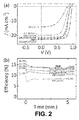
- the resulting device characteristics namely the open circuit voltage V OC , the short cut current (Jsc), the fill factor (FF) the initial efficiency ( ⁇ initial ) and the efficiency after five minutes of maximum power point tracking under constant AM1.5G illumination ( ⁇ MPP ), are listed in the following table.
- FIG. 2 The current/voltage curves ( Fig. 2a ) and the evolution of the efficiency over time ( Fig. 2b ) of photovoltaic cells made from the above solvent mixtures are shown.
- Example 1 was repeated up to step 4, using different desired solvents in step 2.
- Different combinations using GBL, AcOH, EtOH, PrOH, IPA (isopropanol), PC (propylene carbonate), and DMEA (dimethylethanolamine) are considered.
- the ability of the different solvent systems to dissolve the perovskite precursors and to form a perovskite film from the resulting composition is evaluated in the table below. Observations about the appearance of the resulting composition are also included. Solvent System Volume (%) Final Mol Miscible? Perovskite?
- the column “Perovskite?” indicates whether a perovskite film could be obtained from the composition.
- PC used pure or with a >50% solution volume resulted in a cloudy and slightly yellow solution that does not ever dissolve clearly; PC, when used in combination with GBL, also inhibits perovskite formation. It appears therefore that polar aprotic solvents which, when used in absence of other components, cannot dissolve the one or more perovskite precursors, do not lead to the formation of perovskites.
- Fig. 3 SEM images of perovskite layers fabricated from different solvent mixtures are shown; the arrows point towards a pinhole.
- the indicated vol%'s (0, 20, 40) refer to the combined vol%'s of alcohol and acid; if both are present, the alcohol and acid each represent 50 vol% thereof.
- the layer quality compared to that obtained from pure GBL (Fig. 3a) is drastically improved in the layers obtained from GBL/EtOH/AcOH and GBL/PrOH/AcOH, according to the present invention.
- the amount of pinholes is even lower than obtained from pure DMF (Fig. 3h).
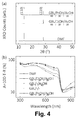
- Fig. 4 X-ray diffraction (Fig. 4a ) and absorption (Fig. 4b ) spectra of perovskite layers fabricated from different solvent mixtures are shown.
- the layers obtained from mixtures according to the present invention are similar to those obtained from pure DMF.
- the absorption spectra are similar in shape; with again the layer obtained from GBL/EtOH/AcOH 60%/20%/20% most closely approximating the case of pure DMF.
- Example 1 was repeated up to step 4, using different desired solvents in step 2. Furthermore, no PbCl 2 was used, so that Pb(oAc) 2 is the only lead perovskite precursor.
- Different combinations using GBL, AcOH, EtOH, PrOH, PC, DMEA, TEG (triethylene glycol), DEG (diethylene glycol), TEA (triethanolamine) and EGBE (ethylene glycol butyl ether) were considered.
- the ability of the different solvent systems to dissolve the perovskite precursors and to form a perovskite film from the resulting composition are again evaluated in the table below. Observations about the appearance of the resulting composition are again included.
- Solvent System Volume (%) Final Mol Miscible? Perovskite?
Landscapes
- Chemical & Material Sciences (AREA)
- Engineering & Computer Science (AREA)
- Materials Engineering (AREA)
- Organic Chemistry (AREA)
- Chemical Kinetics & Catalysis (AREA)
- Physics & Mathematics (AREA)
- Inorganic Chemistry (AREA)
- Power Engineering (AREA)
- Metallurgy (AREA)
- Electrochemistry (AREA)
- Manufacturing & Machinery (AREA)
- Thermal Sciences (AREA)
- General Chemical & Material Sciences (AREA)
- Mechanical Engineering (AREA)
- Microelectronics & Electronic Packaging (AREA)
- Ceramic Engineering (AREA)
- Life Sciences & Earth Sciences (AREA)
- Wood Science & Technology (AREA)
- Crystallography & Structural Chemistry (AREA)
- Spectroscopy & Molecular Physics (AREA)
- Electromagnetism (AREA)
- Inorganic Compounds Of Heavy Metals (AREA)
Priority Applications (6)
| Application Number | Priority Date | Filing Date | Title |
|---|---|---|---|
| EP16153479.7A EP3199664A1 (fr) | 2016-01-29 | 2016-01-29 | Composition de pérovskite multi-solvants |
| US16/069,032 US10614964B2 (en) | 2016-01-29 | 2017-01-17 | Multi-solvent perovskite composition |
| EP17700457.9A EP3408426B1 (fr) | 2016-01-29 | 2017-01-17 | Composition de pérovskite multi-solvants |
| PCT/EP2017/050861 WO2017129441A1 (fr) | 2016-01-29 | 2017-01-17 | Composition de pérovskite multi-solvants |
| CN201780007985.2A CN108495951B (zh) | 2016-01-29 | 2017-01-17 | 多溶剂钙钛矿组合物 |
| RU2018125586A RU2731704C2 (ru) | 2016-01-29 | 2017-01-17 | Композиция для получения перовскитов, содержащая несколько растворителей |
Applications Claiming Priority (1)
| Application Number | Priority Date | Filing Date | Title |
|---|---|---|---|
| EP16153479.7A EP3199664A1 (fr) | 2016-01-29 | 2016-01-29 | Composition de pérovskite multi-solvants |
Publications (1)
| Publication Number | Publication Date |
|---|---|
| EP3199664A1 true EP3199664A1 (fr) | 2017-08-02 |
Family
ID=55310670
Family Applications (2)
| Application Number | Title | Priority Date | Filing Date |
|---|---|---|---|
| EP16153479.7A Withdrawn EP3199664A1 (fr) | 2016-01-29 | 2016-01-29 | Composition de pérovskite multi-solvants |
| EP17700457.9A Active EP3408426B1 (fr) | 2016-01-29 | 2017-01-17 | Composition de pérovskite multi-solvants |
Family Applications After (1)
| Application Number | Title | Priority Date | Filing Date |
|---|---|---|---|
| EP17700457.9A Active EP3408426B1 (fr) | 2016-01-29 | 2017-01-17 | Composition de pérovskite multi-solvants |
Country Status (5)
| Country | Link |
|---|---|
| US (1) | US10614964B2 (fr) |
| EP (2) | EP3199664A1 (fr) |
| CN (1) | CN108495951B (fr) |
| RU (1) | RU2731704C2 (fr) |
| WO (1) | WO2017129441A1 (fr) |
Cited By (1)
| Publication number | Priority date | Publication date | Assignee | Title |
|---|---|---|---|---|
| WO2021040580A3 (fr) * | 2019-08-30 | 2021-05-14 | Сергей Анатольевич ФАТЕЕВ | Procédé de production de monocristaux d'un halogénure complexe organique-inorganique |
Families Citing this family (7)
| Publication number | Priority date | Publication date | Assignee | Title |
|---|---|---|---|---|
| CN107611191B (zh) * | 2017-08-24 | 2019-05-03 | 宁波大学 | 一种无机钙钛矿太阳能电池及其制备方法 |
| CN110379889A (zh) * | 2019-07-31 | 2019-10-25 | 浙江天地环保科技有限公司 | 一种高效率高稳定性全无机钙钛矿太阳能电池的制备方法 |
| CN112864325B (zh) * | 2019-11-26 | 2024-03-29 | 中国石油大学(华东) | 一种多功能三苯胺分子表面钝化钙钛矿薄膜的方法 |
| WO2021207344A1 (fr) * | 2020-04-08 | 2021-10-14 | The Trustees Of Princeton University | Gestion thermique pour dispositifs électroniques pérovskite |
| TWI765376B (zh) | 2020-10-20 | 2022-05-21 | 財團法人工業技術研究院 | 鈣鈦礦薄膜及其前驅組成物、鈣鈦礦薄膜製備方法、包括此薄膜之半導體元件 |
| KR102844846B1 (ko) * | 2022-05-06 | 2025-08-12 | (주)프런티어에너지솔루션 | 그린용매를 베이스로 한 페로브스카이트 전구체 용액 및 이를 이용한 페로브스카이트 박막의 제조방법 |
| CN115594413B (zh) * | 2022-10-21 | 2023-12-29 | 榆林学院 | 一种钠掺杂二维钙钛矿薄膜的制备方法 |
Citations (4)
| Publication number | Priority date | Publication date | Assignee | Title |
|---|---|---|---|---|
| US5527567A (en) * | 1994-09-02 | 1996-06-18 | Ceram Incorporated | Metalorganic chemical vapor deposition of layered structure oxides |
| EP2520692A2 (fr) * | 2011-05-06 | 2012-11-07 | Seiko Epson Corporation | Solution de précurseur de film piézoélectrique, son procédé de fabrication et procédé de fabrication d'un film piézoélectrique |
| WO2013171517A1 (fr) * | 2012-05-18 | 2013-11-21 | Isis Innovation Limited | Dispositifs optoélectroniques à pérovskites organométalliques à anions mixtes |
| EP2897178A2 (fr) * | 2012-09-12 | 2015-07-22 | Korea Research Institute of Chemical Technology | Cellule solaire qui présente une structure absorbant la lumière |
Family Cites Families (8)
| Publication number | Priority date | Publication date | Assignee | Title |
|---|---|---|---|---|
| RU2440292C2 (ru) * | 2009-12-31 | 2012-01-20 | Институт Катализа Им. Г.К. Борескова Сибирского Отделения Российской Академии Наук | Способ получения перовскитов |
| CN102299251B (zh) * | 2011-08-13 | 2012-12-05 | 西北有色金属研究院 | 一种钙钛矿型缓冲层的制备方法 |
| CN102534546A (zh) * | 2012-01-16 | 2012-07-04 | 燕山大学 | 一种玻璃基底上钙钛矿型纳米晶薄膜的制备方法 |
| US20160005547A1 (en) * | 2013-01-10 | 2016-01-07 | Korea Research Institute Of Chemical Technology | Inorganic-organic hybrid solar cell having durability and high performance |
| WO2014109610A1 (fr) * | 2013-01-10 | 2014-07-17 | 한국화학연구원 | Procédé de fabrication d'une cellule solaire hybride organique-inorganique à haut rendement |
| WO2015127494A1 (fr) * | 2014-02-26 | 2015-09-03 | Commonwealth Scientific And Industrial Research Organisation | Procédé de formation d'une couche photoactive d'un dispositif photoactif pérovskite |
| JP6299338B2 (ja) * | 2014-03-31 | 2018-03-28 | セイコーエプソン株式会社 | 圧電素子、液体噴射ヘッド、液体噴射装置及びセンサー |
| US10593816B2 (en) * | 2015-01-08 | 2020-03-17 | Korea Research Institute Of Chemical Technology | Method for manufacturing device comprising inorganic/organic hybrid perovskite compound film and device comprising inorganic/organic hybrid perovskite compound film |
-
2016
- 2016-01-29 EP EP16153479.7A patent/EP3199664A1/fr not_active Withdrawn
-
2017
- 2017-01-17 RU RU2018125586A patent/RU2731704C2/ru active
- 2017-01-17 EP EP17700457.9A patent/EP3408426B1/fr active Active
- 2017-01-17 CN CN201780007985.2A patent/CN108495951B/zh active Active
- 2017-01-17 WO PCT/EP2017/050861 patent/WO2017129441A1/fr not_active Ceased
- 2017-01-17 US US16/069,032 patent/US10614964B2/en active Active
Patent Citations (4)
| Publication number | Priority date | Publication date | Assignee | Title |
|---|---|---|---|---|
| US5527567A (en) * | 1994-09-02 | 1996-06-18 | Ceram Incorporated | Metalorganic chemical vapor deposition of layered structure oxides |
| EP2520692A2 (fr) * | 2011-05-06 | 2012-11-07 | Seiko Epson Corporation | Solution de précurseur de film piézoélectrique, son procédé de fabrication et procédé de fabrication d'un film piézoélectrique |
| WO2013171517A1 (fr) * | 2012-05-18 | 2013-11-21 | Isis Innovation Limited | Dispositifs optoélectroniques à pérovskites organométalliques à anions mixtes |
| EP2897178A2 (fr) * | 2012-09-12 | 2015-07-22 | Korea Research Institute of Chemical Technology | Cellule solaire qui présente une structure absorbant la lumière |
Cited By (1)
| Publication number | Priority date | Publication date | Assignee | Title |
|---|---|---|---|---|
| WO2021040580A3 (fr) * | 2019-08-30 | 2021-05-14 | Сергей Анатольевич ФАТЕЕВ | Procédé de production de monocristaux d'un halogénure complexe organique-inorganique |
Also Published As
| Publication number | Publication date |
|---|---|
| CN108495951A (zh) | 2018-09-04 |
| RU2731704C2 (ru) | 2020-09-08 |
| CN108495951B (zh) | 2021-02-26 |
| RU2018125586A3 (fr) | 2020-05-28 |
| US20180358184A1 (en) | 2018-12-13 |
| WO2017129441A1 (fr) | 2017-08-03 |
| US10614964B2 (en) | 2020-04-07 |
| EP3408426B1 (fr) | 2020-04-22 |
| RU2018125586A (ru) | 2020-01-13 |
| EP3408426A1 (fr) | 2018-12-05 |
Similar Documents
| Publication | Publication Date | Title |
|---|---|---|
| EP3408426B1 (fr) | Composition de pérovskite multi-solvants | |
| Ghosh et al. | Antisolvents in perovskite solar cells: importance, issues, and alternatives | |
| Chi et al. | Application of perovskite quantum dots as an absorber in perovskite solar cells | |
| Saliba et al. | How to Make over 20% Efficient Perovskite Solar Cells in Regular (n–i–p) and Inverted (p–i–n) Architectures | |
| Song et al. | Importance of reducing vapor atmosphere in the fabrication of tin-based perovskite solar cells | |
| EP4002505B1 (fr) | Liquides ioniques fonctionnalisés en tant que stabilisants pour des cellules solaires de pérovskite | |
| Singh et al. | Stable triple-cation (Cs+–MA+–FA+) perovskite powder formation under ambient conditions for hysteresis-free high-efficiency solar cells | |
| US20180005762A1 (en) | Methods for making perovskite solar cells having improved hole-transport layers | |
| EP3940806B1 (fr) | Procédé de modification de la structure de films de pérovskite | |
| JP2018113305A (ja) | 光電変換素子及び太陽電池 | |
| JP7619425B2 (ja) | 光電変換素子 | |
| Zhang et al. | Efficient nonlead double perovskite solar cell with multiple hole transport layers | |
| CN110556481B (zh) | 一种铅锡共混钙钛矿层及其制备方法和应用 | |
| Baranwal et al. | Fabrication of fully non-vacuum processed perovskite solar cells using an inorganic CuSCN hole-transporting material and carbon-back contact | |
| CN111463349A (zh) | 一种提高钙钛矿太阳能电池稳定性的方法 | |
| JP2020137161A (ja) | 光電変換装置 | |
| Chang et al. | The Cesium doping using the nonstoichiometric precursor for improved CH3NH3PbI3 perovskite films and solar cells in ambient air | |
| Nishimura et al. | Long aliphatic chain-based spontaneous perovskite passivator: trade-off between the passivation effect and hole-transport material compatibility | |
| KR102810697B1 (ko) | 유무기 페로브스카이트 소자의 안정성을 향상시키는 페로브스카이트 버퍼레이어 형성방법 | |
| JP7110537B2 (ja) | 光吸収層用前駆体、これを用いた有機-無機複合太陽電池の製造方法および有機-無機複合太陽電池 | |
| CN118973277B (zh) | 一种掺杂3-三氟甲基吡啶的含锡钙钛矿太阳能电池及其制备方法 | |
| CN116133441B (zh) | 一种钙钛矿太阳能电池及其制备方法 | |
| JP6835417B2 (ja) | 有機−無機複合太陽電池の製造方法 | |
| JP6657841B2 (ja) | 光電変換素子及び太陽電池 | |
| CN114497371A (zh) | 一种卤化亚锡溶液及其制备方法与应用 |
Legal Events
| Date | Code | Title | Description |
|---|---|---|---|
| PUAI | Public reference made under article 153(3) epc to a published international application that has entered the european phase |
Free format text: ORIGINAL CODE: 0009012 |
|
| STAA | Information on the status of an ep patent application or granted ep patent |
Free format text: STATUS: THE APPLICATION HAS BEEN PUBLISHED |
|
| AK | Designated contracting states |
Kind code of ref document: A1 Designated state(s): AL AT BE BG CH CY CZ DE DK EE ES FI FR GB GR HR HU IE IS IT LI LT LU LV MC MK MT NL NO PL PT RO RS SE SI SK SM TR |
|
| AX | Request for extension of the european patent |
Extension state: BA ME |
|
| STAA | Information on the status of an ep patent application or granted ep patent |
Free format text: STATUS: THE APPLICATION IS DEEMED TO BE WITHDRAWN |
|
| 18D | Application deemed to be withdrawn |
Effective date: 20180203 |