EP3199670B1 - Verfahren zur herstellung eines gruppe-iii-nitrid-kristalls, verfahren zur herstellung eines halbleiterbauelements und verwendung einer vorrichtung zur herstellung des gruppe-iii-nitrid-kristalls - Google Patents
Verfahren zur herstellung eines gruppe-iii-nitrid-kristalls, verfahren zur herstellung eines halbleiterbauelements und verwendung einer vorrichtung zur herstellung des gruppe-iii-nitrid-kristalls Download PDFInfo
- Publication number
- EP3199670B1 EP3199670B1 EP15855510.2A EP15855510A EP3199670B1 EP 3199670 B1 EP3199670 B1 EP 3199670B1 EP 15855510 A EP15855510 A EP 15855510A EP 3199670 B1 EP3199670 B1 EP 3199670B1
- Authority
- EP
- European Patent Office
- Prior art keywords
- group iii
- gas
- crystal
- iii element
- element nitride
- Prior art date
- Legal status (The legal status is an assumption and is not a legal conclusion. Google has not performed a legal analysis and makes no representation as to the accuracy of the status listed.)
- Active
Links
Images


Classifications
-
- C—CHEMISTRY; METALLURGY
- C30—CRYSTAL GROWTH
- C30B—SINGLE-CRYSTAL GROWTH; UNIDIRECTIONAL SOLIDIFICATION OF EUTECTIC MATERIAL OR UNIDIRECTIONAL DEMIXING OF EUTECTOID MATERIAL; REFINING BY ZONE-MELTING OF MATERIAL; PRODUCTION OF A HOMOGENEOUS POLYCRYSTALLINE MATERIAL WITH DEFINED STRUCTURE; SINGLE CRYSTALS OR HOMOGENEOUS POLYCRYSTALLINE MATERIAL WITH DEFINED STRUCTURE; AFTER-TREATMENT OF SINGLE CRYSTALS OR A HOMOGENEOUS POLYCRYSTALLINE MATERIAL WITH DEFINED STRUCTURE; APPARATUS THEREFOR
- C30B29/00—Single crystals or homogeneous polycrystalline material with defined structure characterised by the material or by their shape
- C30B29/10—Inorganic compounds or compositions
- C30B29/40—AIIIBV compounds wherein A is B, Al, Ga, In or Tl and B is N, P, As, Sb or Bi
- C30B29/403—AIII-nitrides
- C30B29/406—Gallium nitride
-
- C—CHEMISTRY; METALLURGY
- C23—COATING METALLIC MATERIAL; COATING MATERIAL WITH METALLIC MATERIAL; CHEMICAL SURFACE TREATMENT; DIFFUSION TREATMENT OF METALLIC MATERIAL; COATING BY VACUUM EVAPORATION, BY SPUTTERING, BY ION IMPLANTATION OR BY CHEMICAL VAPOUR DEPOSITION, IN GENERAL; INHIBITING CORROSION OF METALLIC MATERIAL OR INCRUSTATION IN GENERAL
- C23C—COATING METALLIC MATERIAL; COATING MATERIAL WITH METALLIC MATERIAL; SURFACE TREATMENT OF METALLIC MATERIAL BY DIFFUSION INTO THE SURFACE, BY CHEMICAL CONVERSION OR SUBSTITUTION; COATING BY VACUUM EVAPORATION, BY SPUTTERING, BY ION IMPLANTATION OR BY CHEMICAL VAPOUR DEPOSITION, IN GENERAL
- C23C16/00—Chemical coating by decomposition of gaseous compounds, without leaving reaction products of surface material in the coating, i.e. chemical vapour deposition [CVD] processes
- C23C16/22—Chemical coating by decomposition of gaseous compounds, without leaving reaction products of surface material in the coating, i.e. chemical vapour deposition [CVD] processes characterised by the deposition of inorganic material, other than metallic material
- C23C16/30—Deposition of compounds, mixtures or solid solutions, e.g. borides, carbides, nitrides
- C23C16/34—Nitrides
-
- C—CHEMISTRY; METALLURGY
- C30—CRYSTAL GROWTH
- C30B—SINGLE-CRYSTAL GROWTH; UNIDIRECTIONAL SOLIDIFICATION OF EUTECTIC MATERIAL OR UNIDIRECTIONAL DEMIXING OF EUTECTOID MATERIAL; REFINING BY ZONE-MELTING OF MATERIAL; PRODUCTION OF A HOMOGENEOUS POLYCRYSTALLINE MATERIAL WITH DEFINED STRUCTURE; SINGLE CRYSTALS OR HOMOGENEOUS POLYCRYSTALLINE MATERIAL WITH DEFINED STRUCTURE; AFTER-TREATMENT OF SINGLE CRYSTALS OR A HOMOGENEOUS POLYCRYSTALLINE MATERIAL WITH DEFINED STRUCTURE; APPARATUS THEREFOR
- C30B25/00—Single-crystal growth by chemical reaction of reactive gases, e.g. chemical vapour-deposition growth
- C30B25/02—Epitaxial-layer growth
- C30B25/14—Feed and outlet means for the gases; Modifying the flow of the reactive gases
-
- C—CHEMISTRY; METALLURGY
- C30—CRYSTAL GROWTH
- C30B—SINGLE-CRYSTAL GROWTH; UNIDIRECTIONAL SOLIDIFICATION OF EUTECTIC MATERIAL OR UNIDIRECTIONAL DEMIXING OF EUTECTOID MATERIAL; REFINING BY ZONE-MELTING OF MATERIAL; PRODUCTION OF A HOMOGENEOUS POLYCRYSTALLINE MATERIAL WITH DEFINED STRUCTURE; SINGLE CRYSTALS OR HOMOGENEOUS POLYCRYSTALLINE MATERIAL WITH DEFINED STRUCTURE; AFTER-TREATMENT OF SINGLE CRYSTALS OR A HOMOGENEOUS POLYCRYSTALLINE MATERIAL WITH DEFINED STRUCTURE; APPARATUS THEREFOR
- C30B25/00—Single-crystal growth by chemical reaction of reactive gases, e.g. chemical vapour-deposition growth
- C30B25/02—Epitaxial-layer growth
- C30B25/18—Epitaxial-layer growth characterised by the substrate
- C30B25/20—Epitaxial-layer growth characterised by the substrate the substrate being of the same materials as the epitaxial layer
-
- C—CHEMISTRY; METALLURGY
- C30—CRYSTAL GROWTH
- C30B—SINGLE-CRYSTAL GROWTH; UNIDIRECTIONAL SOLIDIFICATION OF EUTECTIC MATERIAL OR UNIDIRECTIONAL DEMIXING OF EUTECTOID MATERIAL; REFINING BY ZONE-MELTING OF MATERIAL; PRODUCTION OF A HOMOGENEOUS POLYCRYSTALLINE MATERIAL WITH DEFINED STRUCTURE; SINGLE CRYSTALS OR HOMOGENEOUS POLYCRYSTALLINE MATERIAL WITH DEFINED STRUCTURE; AFTER-TREATMENT OF SINGLE CRYSTALS OR A HOMOGENEOUS POLYCRYSTALLINE MATERIAL WITH DEFINED STRUCTURE; APPARATUS THEREFOR
- C30B9/00—Single-crystal growth from melt solutions using molten solvents
- C30B9/02—Single-crystal growth from melt solutions using molten solvents by evaporation of the molten solvent
-
- H—ELECTRICITY
- H10—SEMICONDUCTOR DEVICES; ELECTRIC SOLID-STATE DEVICES NOT OTHERWISE PROVIDED FOR
- H10D—INORGANIC ELECTRIC SEMICONDUCTOR DEVICES
- H10D62/00—Semiconductor bodies, or regions thereof, of devices having potential barriers
- H10D62/80—Semiconductor bodies, or regions thereof, of devices having potential barriers characterised by the materials
- H10D62/85—Semiconductor bodies, or regions thereof, of devices having potential barriers characterised by the materials being Group III-V materials, e.g. GaAs
- H10D62/8503—Nitride Group III-V materials, e.g. AlN or GaN
-
- H—ELECTRICITY
- H10—SEMICONDUCTOR DEVICES; ELECTRIC SOLID-STATE DEVICES NOT OTHERWISE PROVIDED FOR
- H10H—INORGANIC LIGHT-EMITTING SEMICONDUCTOR DEVICES HAVING POTENTIAL BARRIERS
- H10H20/00—Individual inorganic light-emitting semiconductor devices having potential barriers, e.g. light-emitting diodes [LED]
- H10H20/80—Constructional details
- H10H20/81—Bodies
- H10H20/822—Materials of the light-emitting regions
- H10H20/824—Materials of the light-emitting regions comprising only Group III-V materials, e.g. GaP
- H10H20/825—Materials of the light-emitting regions comprising only Group III-V materials, e.g. GaP containing nitrogen, e.g. GaN
-
- H—ELECTRICITY
- H10—SEMICONDUCTOR DEVICES; ELECTRIC SOLID-STATE DEVICES NOT OTHERWISE PROVIDED FOR
- H10P—GENERIC PROCESSES OR APPARATUS FOR THE MANUFACTURE OR TREATMENT OF DEVICES COVERED BY CLASS H10
- H10P14/00—Formation of materials, e.g. in the shape of layers or pillars
- H10P14/20—Formation of materials, e.g. in the shape of layers or pillars of semiconductor materials
- H10P14/24—Formation of materials, e.g. in the shape of layers or pillars of semiconductor materials using chemical vapour deposition [CVD]
-
- H—ELECTRICITY
- H10—SEMICONDUCTOR DEVICES; ELECTRIC SOLID-STATE DEVICES NOT OTHERWISE PROVIDED FOR
- H10P—GENERIC PROCESSES OR APPARATUS FOR THE MANUFACTURE OR TREATMENT OF DEVICES COVERED BY CLASS H10
- H10P14/00—Formation of materials, e.g. in the shape of layers or pillars
- H10P14/20—Formation of materials, e.g. in the shape of layers or pillars of semiconductor materials
- H10P14/34—Deposited materials, e.g. layers
- H10P14/3402—Deposited materials, e.g. layers characterised by the chemical composition
- H10P14/3414—Deposited materials, e.g. layers characterised by the chemical composition being group IIIA-VIA materials
- H10P14/3416—Nitrides
Definitions
- the present invention relates to a method for producing a Group III element nitride crystal, a method for producing a semiconductor device, and the use of a Group III element nitride crystal production device.
- a Group III nitride semiconductor such as gallium nitride (GaN) has been used widely as a material for various semiconductor devices such as a laser diode (LD) and a light-emitting diode (LED).
- LD laser diode
- LED light-emitting diode
- the laser diode (LD) that emits blue light is applied to a high-density optical disc or a display
- a light-emitting diode (LED) that emits blue light is applied to a display or illumination.
- an ultraviolet LD is expected to be applied to biotechnology and the like, and an ultraviolet LED is expected as an ultraviolet source of a fluorescent lamp.
- Examples of a commonly-used method for producing a Group III nitride (e.g., GaN) crystal substrate include vapor deposition (vapor-phase epitaxial growth, i.e., Hydride Vapor Phase Epitaxy) and liquid deposition. Each deposition method has specific characteristics. The vapor deposition can be performed easily and thus is suitable for mass production. Examples of the vapor deposition include halide vapor phase epitaxy (Patent Document 1) and metalorganic chemical vapor deposition (MOCVD).
- Patent Document 1 halide vapor phase epitaxy
- MOCVD metalorganic chemical vapor deposition
- Patent Document 3 describes a method of producing a Group III nitride crystal that prevents a halogen-containing by-product from adversely affecting crystal generation.
- the method of producing a Group III nitride crystal includes a step of causing a Group III metal to react with an oxidizing gas and nitrogen-containing gas, thereby producing a Group III nitride crystal.
- Patent Document 4 describes a nitride semiconductor crystal, manufacturing method, and manufacturing apparatus.
- Patent Document 4 relates to a nitride semiconductor crystal that has a diameter of four inches or more and is warped to have a curvature radius of 100 m or more, and has an impurity concentration of 1 x 10 17 / cm 3 or lower.
- the document also describes a manufacturing method for a nitride semiconductor crystal includes providing a substrate, feeding a gallium trihalide gas having a partial pressure of 9.0 x 10 -3 atm or higher onto the substrate, and growing a GaN crystal in the -C-axis direction on the substrate, where a growth temperature for the GaN crystal is 1200°C or higher, or a manufacturing method for a nitride semiconductor crystal includes providing a substrate, feeding an aluminum trihalide gas having a partial pressure of 9.0 x 10 -3 atm or higher onto the substrate, and growing an AIN crystal in the -C-axis direction on the substrate, where a growth temperature for the AIN crystal is 1400°C or higher.
- Patent Document 5 discloses a nitride semiconductor crystal producing method, comprising growing a nitride semiconductor crystal over a seed crystal substrate , while applying an etching action to an outer end of the seed crystal substrate during the growing of the nitride semiconductor crystal.
- Non-Patent Document 1 describes the effect of H2 carrier gas on the physical properties of a GaN layer grown using Ga2O vapor and NH3.
- Non-Patent Document 2 describes the growth of GaN films with low oxygen concentration using Ga2O vapor and NH3.
- the Group III element nitride crystal is generally a hexagonal crystal.
- Crystal planes of the hexagonal crystal include an a-plane, an m-plane, and a c-plane.
- the c-plane is suitable as a crystal growth plane.
- the c-plane is thus used as a crystal growth plane in the method for producing an industrially applicable Group III element nitride crystal.
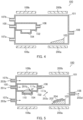
- Steps of the commonly-used method for producing a Group III element nitride crystal are schematically shown in step cross-sectional views of (a) to (e) in FIG. 22A .
- FIG. 22B (a) to (e) are perspective views of the respective steps in (a) to (e) in FIG. 22A .
- a Group III element nitride seed crystal (hereinafter also merely referred to as a "seed crystal") 11 is disposed on a substrate 10.
- seed crystal a Group III element nitride seed crystal
- FIG. 22B that is a perspective view of (a) in FIG. 22A , the substrate 10 is omitted for visibility. The same applies to (b) to (e) in FIG. 22B .
- a Group III element nitride crystal (hereinafter also merely referred to as a "crystal) 12 is then grown from the seed crystal 11. As shown in (c) to (d) in FIG. 22A ((c) to (d) in FIG. 22B) , the crystal 12 is then further grown to be big. As shown in (d) in each of FIGs. 22A and 22B , the crystal 12 is thereafter sliced laterally along dotted lines 13 and 14. A plate-like Group III element nitride crystal substrate 12a as shown in (e) in eacn of FIGs. 22A and 22B thus can be obtained.
- the diameter of the grown (deposited) crystal is reduced toward the top (newly deposited part) as shown in FIGs. 22A and 22B .
- This crystal growth thus has a limitation in increasing the size of the crystal.
- the crystal 12 is grown in the lateral direction (direction parallel with the plane of the substrate 10) as shown in FIGs. 22A and 22B , it is difficult to obtain a crystal having a size in the lateral direction that is larger than the substrate 10.
- the crystal 12 thus have a higher quality without crystal defects and the like taken over from the substrate 10.
- the diameter of the grown (deposited) crystal is reduced toward the top (newly deposited part). It is thus difficult to obtain a high-quality, large crystal.
- a plane on the -c-plane side that is a plane on the opposite side of the c-plane is considered to be used as a crystal growth plane.
- the c-plane that is a crystal growth plane in the commonly-used crystal growth steps as shown in (a) to (e) in each of F FIGs. 22A and 22B is referred to as a +c-plane to differentiate from the -c-plane.
- Step cross-sectional views (a) to (e) in FIG. 1A and perspective views (a) to (e) in FIG. 1B schematically illustrate steps in the method for producing a Group III element nitride crystal using the -c-plane as a crystal growth plane.
- this method for producing a Group III element nitride crystal is the same as the method shown in (a) to (e) in each of FIGs. 22A and 22B except that the -c-plane is used as a crystal growth plane as a substitute for the +c-plane.
- a crystal grown by the commonly-used method shown in (a) to (e) in each of FIG. 22A and 22B may be inversed, and the -c-plane that is a plane opposite to the +c-plane may be used as a crystal growth plane, to use the -c-plane as a crystal growth plane as described above.
- a crystal 12 in the state shown in (b) or (c) in FIG. 22A ((b) or (c) in FIG. 22B ) is inversed to be the crystal 12 in the state of (b) or (c) in FIG. 1A (b) or (c) in FIG. 1B) and is then used as it is in the subsequent steps.
- the present invention provides a method for producing a Group III element nitride crystal in which a Group III element nitride crystal is grown using a plane on the -c-plane side as a crystal growth plane.
- the present invention further provides a a method for producing a semiconductor device, and the use of a Group III element nitride crystal production device in the production method of the present invention.
- the present invention provides a method for producing a Group III element nitride crystal, the method including:
- the present invention also provides a method for producing a Group III element nitride crystal, the method comprising:
- the present invention further provides a method for producing a semiconductor device including a Group III element nitride crystal, the method comprising: producing a Group III element nitride crystal by the method for producing a Group III element nitride crystal of the present invention, wherein the Group III element nitride crystal is a semiconductor.
- the present invention further provides the use of a first Group III element nitride crystal production device in the method for producing a Group III element nitride crystal of the present invention, including: a vapor phase growth unit configured to grow a Group III element nitride crystal on a Group III element nitride seed crystal by vapor deposition; and a liquid raw material supply unit configured to continuously supply a liquid form of gallium metal to the vapor phase growth unit.
- the present invention further provides the use of a second Group III element nitride crystal production device in the method for producing a Group III element nitride crystal of the present invention, wherein
- the method for producing a Group III element nitride crystal of the present invention can grow a Group III element nitride crystal using a plane on the -c-plane side as a crystal growth plane.
- the present invention can further provide a method for producing a semiconductor device, and the use of a Group III element nitride crystal production device in the production method of the present invention.
- the production method of the present invention can be performed as in the step cross-sectional views of (a) to (e) in FIG. 1A and perspective views of (a) to (e) in FIG. 1B , for example. That is, first, as shown in (a) in FIG. 1A , a Group III element nitride seed crystal 11 is disposed on a substrate 10.
- the material of the substrate 10 is not limited to particular materials and preferably contains, for example, at least one selected from the group consisting of an oxide of Al x Ga y In 1-x-y N (0 ⁇ x ⁇ 1, 0 ⁇ y ⁇ 1, x + y ⁇ 1), diamond-like carbon, silicon nitride, silicon oxide, silicon oxynitride, aluminium oxide, aluminium oxynitride, silicon carbide, yttrium oxide, yttrium aluminium garnet (YAG), tantalum, rhenium, and tungsten.
- an oxide of Al x Ga y In 1-x-y N (0 ⁇ x ⁇ 1, 0 ⁇ y ⁇ 1, x + y ⁇ 1)
- diamond-like carbon silicon nitride, silicon oxide, silicon oxynitride, aluminium oxide, aluminium oxynitride, silicon carbide, yttrium oxide, yttrium aluminium garnet (YAG), tantalum, r
- Examples of the material of the substrate 10 further include sapphire, Group III nitride, gallium arsenide (GaAs), silicon (Si), silicon carbide (SiC), magnesium oxide (MgO), zinc oxide (ZnO), gallium phosphide (GaP), zirconium diboride (ZrB 2 ), lithium dioxogallate (LiGaO 2 ), BP, MoS 2 , LaAlO 3 , NbN, MnFe 2 O 4 , ZnFe 2 O 4 , ZrN, TiN, MgAl 2 O 4 , NdGaO 3 , LiAlO 2 , ScAlMgO 4 , and Ca 8 La 2 (PO 4 ) 6 O 2 .
- GaAs gallium arsenide
- Si silicon
- SiC silicon carbide
- MgO magnesium oxide
- ZnO zinc oxide
- ZrB 2 zirconium diboride
- the material of the substrate 10 may be a Group III nitride as mentioned above, and in this case, the substrate 10 itself may also serve as the Group III element nitride seed crystal 11.
- the material of the Group III element nitride seed crystal 11 may be identical to or different from and is preferably the same as that of a Group III element nitride crystal 12 to be grown thereon.
- the Group III element nitride crystal 12 is then grown from the seed crystal 11 as shown in (b) in each o f FIGs. 1A and 1B .
- the crystal 12 is then further grown to be big as shown in (c) to (d) in each of f FIGs. 1A and 1B .
- the crystal 12 is thereafter laterally sliced along dotted lines 13 and 14 as shown in (d) in each of f FIGs. 1A and 1B .
- a plate-like Group III element nitride crystal substrate 12a can be obtained as shown in (e) in each of f FIGs. 1A and 1B .
- a crystal grown by a commonly-used method may be inversed as mentioned above, and the -c-plane that is a plane on the inverse side may be used as a crystal growth plane.
- the crystal 12 in the state of ( b) or (c) in FIG. 22A ((b) or (c) in FIG. 22B ) may be inversed and then cut into an appropriate size to obtain a seed crystal 11 of (a) in FIG. 1A ( (a) in FIG. 1B ).
- the crystal 12 in the state of (b) or (c) in FIG. 22A ((b) or (c) in FIG. 22B) may be inversed and used as it is in the subsequent steps
- the production method of the present invention allows the diameter of the Group III element nitride crystal 12 to increase as growing as described in the step drawings in FIGs. 1A and 1B . Accordingly, it is possible to obtain a high-quality Group III element nitride crystal having a small density of crystal defect (with less crystal defects per unit area of the Group III element nitride crystal 12), derived from the seed crystal 11 (taken over from the seed crystal 11), for example.
- the crystal growth temperature in the vapor phase growth step of the production method of the present invention is 1200°C or more.
- the crystal growth plane thus can be prevented from being inverted from the -c-plane to the +c-plane, and a Group III element nitride crystal can be grown on the -c-plane. Therefore, a high-quality, large Group III element nitride crystal can be produced, for example.
- the crystal growth temperature is preferably 1300°C or more, yet more preferably 1400°C or more, particularly preferably 1500°C or more.
- the upper limit of the crystal growth temperature is not limited to particular temperatures and is, for example, 2000°C or less.
- the crystal growth rate in the vapor phase growth step is not limited to particular rates and is preferably not too high, which further prevents the phenomenon (polarity inversion) where the crystal growth plane is inverted from the -c-plane to the +c-plane.
- the crystal growth rate is not limited to particular rates and is, for example, 2 mm/h or less, preferably 200 ⁇ m/h or less, more preferably 50 ⁇ m/h or less as a thickness increase rate of the Group III element nitride crystal per 1 hour, assuming that the crystal growth temperature is 1200°C or more and less than 1250°C.
- the crystal growth rate is, for example, 3 mm/h or less, preferably 300 ⁇ m/h or less, more preferably 30 ⁇ m/h or less, assuming that the crystal growth temperature is 1250°C or more and less than 1300°C.
- the crystal growth rate is, for example, 4 mm/h or less, preferably 400 ⁇ m/h or less, more preferably 40 ⁇ m/h or less, assuming that the crystal growth temperature is 1300°C or more and less than 1400°C.
- the crystal growth rate is, for example, 5 mm/h or less, preferably 500 ⁇ m/h or less, more preferably 50 ⁇ m/h or less, assuming that the crystal growth temperature is 1400°C or more.
- the lower limit of the crystal growth rate is not limited to particular rates and is preferably 10 ⁇ m/h to increase crystal production efficiency.
- the crystal growth plane of the Group III element nitride seed crystal is, as mentioned above, a plane on the -c-plane side.
- the Group III element nitride crystal is grown in an approximately -c direction in the vapor phase growth step.
- the crystal growth plane is the "plane on the -c-plane side”
- the growth direction of the Group III element nitride crystal is an "approximately -c direction" with reference to the drawings.
- FIG. 2 is a cross-sectional view schematically illustrating a structure of a Group III element nitride seed crystal for use in the production method of the present invention. As shown in FIG.
- a seed crystal 11 has a c-plane (a plane perpendicular to the plane of the paper along the dotted line of FIG. 2 or a plane parallel therewith). As shown in FIG. 2 , the c-plane has a -c-plane side (the upper side of the paper) and +c-plane side (the lower side of the paper). In the present invention, a plane 11a on the -c-plane side on the surface of the seed crystal 11 is used as a crystal growth plane.
- the Group III element nitride crystal is grown in an approximately -c direction, i.e., the -c direction (a direction perpendicular to the -c-plane and toward the -c-plane side) or a direction approximately agreeing with the -c direction.
- the state of the "approximately -c direction" as the growth direction of the Group III element nitride crystal i.e., the state of "a direction approximately agreeing with” the -c direction is the state of an angle formed between the growth direction of the crystal and the -c direction of 10° or less, for example preferably 5° or less, more preferably 3° or less, yet more preferably 1° or less and is ideally the state of the angle of 0° (i.e., the growth direction of the crystal completely agreeing with the -c direction).
- the crystal growth plane of the Group III element nitride seed crystal may completely agree with the -c-plane or may be a plane approximately parallel with the -c-plane, for example.
- the Group III element nitride crystal is easily grown in the -c direction (a direction approximately perpendicular to the -c-plane).
- FIG. 2 shows an example where the crystal growth plane 11a is approximately parallel with the -c-plane.
- the state where the crystal growth plane is "approximately parallel" with the -c-plane is a state of an angle formed between the crystal growth plane and the -c-plane of 10° or less, for example preferably 5° or less, more preferably 3° or less, yet more preferably 1°or less and is ideally the state of the angle of 0° (i.e., the crystal growth plane completely agreeing with the -c-plane).
- the crystal growth plane of the Group III element nitride seed crystal may be an uneven plane.
- FIG. 3 is a cross-sectional view of such a Group III element nitride seed crystal.
- FIG. 3 is the same as FIG. 2 except that the crystal growth plane 11a in the Group III element nitride seed crystal 11 has asperities.
- the asperities in the crystal growth plane 11a have, as shown in FIG. 3 , planes largely tilted with respect to the -c-plane.
- the entire crystal growth plane 11a is approximately parallel with the -c-plane.
- the entire crystal growth plane is preferably approximately parallel with the -c-plane.
- the shapes of the asperities are not limited to those in FIG. 3 and may be any shapes.
- the plane on the -c-plane side (e.g., the -c-plane or a plane approximately parallel with the -c-plane) may be partially inverted to a plane on the +c-plane side by polarity inversion.
- the proportion of the plane whose polarity is inverted is preferably 50% or less, more preferably 30% or less, yet more preferably 10% or less, ideally 0 in the entire area of the crystal growth plane of the Group III element nitride seed crystal.
- the present invention can prevent the polarity inversion of the crystal growth plane in crystal growth, and however, the polarity inversion may occur in crystal growth.
- the proportion of the plane whose polarity is inverted is preferably 50% or less, more preferably 30% or less, yet more preferably 10% or less, ideally 0, in, for example, the entire area of a plane 11 ⁇ m deposited (grown) on the crystal growth plane of the Group III element nitride seed crystal.
- the Group III element nitride seed crystal for use in the vapor phase growth step may be produced by liquid deposition.
- the liquid deposition is not limited to particular methods, and a Group III element nitride crystal (the Group III element nitride seed crystal for use in the vapor phase growth step) may be produced by, for example, bringing the surface of a Group III element nitride seed crystal for use in the liquid deposition into contact with an alkali metal (e.g., sodium) melt to cause, in an atmosphere containing nitrogen, a Group III element and the nitrogen to react with each other in the alkali metal melt. More specifically, for example, any method described in JP 2002-293696 A , Japanese Patent No.
- an alkali metal e.g., sodium
- the vapor phase growth step is, as mentioned above, the following vapor phase growth step (A) or (B).
- the vapor phase growth step (A) is a step of causing a Group III metal, an oxidant that is an oxygen-containing compound, and a nitrogen-containing gas to react with one another to grow the Group III element nitride crystal.
- the vapor phase growth step (B) includes: a reduced product gas generation step of causing a Group III element oxide and a reducing gas to react with each other to generate a gas of a reduced product of the Group III element oxide; and a crystal generation step of causing the gas of the reduced product and a nitrogen-containing gas to react with each other to generate the Group III element nitride crystal.
- the Group III metal is preferably at least one selected from the group consisting of gallium, indium, and aluminium, particularly preferably gallium.
- the vapor phase growth step (A) in the production method of the present invention includes a Group III metal oxidation product gas generation step of causing the Group III metal and the oxidant to react with each other to generate a Group III metal oxidization product gas; and a Group III element nitride crystal generation step of causing the Group III metal oxidization product gas and the nitrogen-containing gas to react with each other to generate the Group III element nitride crystal.
- the Group III metal is caused to react with the oxidant under heating in the Group III metal oxidation product gas generation step.
- the Group III metal oxidization product gas is a Group III metal oxide gas.
- the Group III metal is gallium, and the Group III metal oxidization product gas is a Ga 2 O gas.
- the oxidant in the vapor phase growth step (A) is an oxygen-containing compound.
- the oxygen-containing compound is an oxidizing gas that is at least one selected from the group consisting of a H 2 O gas, an O 2 gas, a CO 2 gas, and a CO gas, particularly preferably an H 2 O gas.
- the nitrogen-containing gas in the vapor phase growth step (A) is preferably at least one selected from the group consisting of N 2 , NH 3, a hydrazine gas, and an alkylamine gas.
- the volume of the oxidizing gas is not limited to particular volumes, and the proportion of the volume of the oxidizing gas in the total volume of the oxidizing gas and the nitrogen-containing gas is, for example, more than 0% to less than 100%, preferably 0.001% or more to less than 100%, more preferably 0.01% to 95%, yet more preferably 0.1% to 80%, yet more preferably 0.1% to 60%.
- the reaction is preferably performed in the presence of a reducing gas in a reaction system.
- the reducing gas is preferably a hydrogencontaining gas, more preferably at least one selected from the group consisting of an H 2 gas, a carbon monoxide (CO) gas, a hydrocarbon gas, an H 2 S gas, an SO 2 gas, and an NH 3 gas.
- the hydrocarbon gas is preferably at least one of a methane gas or an ethane gas. It is more preferred that the oxidant is the oxidizing gas defined above, and the reducing gas is mixed with the oxidizing gas in the crystal growth step (A).
- the reaction in the presence of a reducing gas is preferably performed at 650°C or more.
- the Group III element nitride crystal may be generated under pressure or reduced pressure or without pressurization and depressurization.
- the Group III element oxide is then preferably caused to react with the reducing gas under heating.
- the Group III element oxide is Ga 2 O 3
- the gas of the reduced product is Ga 2 O gas
- the Group III element nitride crystal is a GaN crystal.
- the reduced product gas generation step in the vapor phase growth step (B) is preferably performed in an atmosphere of a mixed gas of a reducing gas and an inactive gas. It is preferred that the proportion of the reducing gas in the total amount of the mixed gas is 3% or more to less than 100 vol%, and the proportion of the inactive gas in the total amount of the mixed gas is more than 0 to 97 vol% or less. It is more preferred that the inactive gas includes nitrogen gas.
- the reducing gas preferably includes a hydrogen gas.
- the nitrogen-containing gas preferably includes an ammonia gas
- the crystal generation step in the vapor phase growth step (B) may be performed under pressure or reduced pressure or without pressurization and depressurization, for example.
- the production method of the present invention may or may not include a step(s) in addition to the vapor phase growth step, as appropriate.
- the production method of the present invention may or may not further include a step (liquid phase growth step) of producing the Group III element nitride seed crystal for use in the vapor phase growth step by liquid deposition.
- the production method of the present invention preferably further includes a slicing step of slicing the Group III element nitride crystal to cut at least one Group III element nitride crystal substrate out.
- the Group III element nitride crystal is preferably represented by Al x Ga y In 1-x-y N (0 ⁇ x ⁇ 1, 0 ⁇ y ⁇ 1, x + y ⁇ 1) and is particularly preferably GaN.
- a Group III element nitride crystal is grown on a crystal growth plane of a Group III element nitride seed crystal by vapor deposition.
- the crystal growth plane is a -c-plane or a plane approximately parallel with the -c-plane.
- the vapor phase growth step is, as mentioned above, the vapor phase growth step (A) or the vapor phase growth step (B).
- the vapor phase growth step (A) is, as mentioned above, a step of causing a Group III metal, an oxidant that is an oxygen-containing compound, and a nitrogen-containing gas to react with one another to grow the Group III element nitride crystal.
- the vapor phase growth step (B) includes, as mentioned above, a reduced product gas generation step of causing a Group III element oxide and a reducing gas to react with each other to generate a gas of a reduced product of the Group III element oxide and a crystal generation step of causing the gas of the reduced product and a nitrogen-containing gas to react with each other to generate the Group III element nitride crystal.
- the vapor phase growth steps (A) and (B) are not limited to particular steps and may be, for example, a commonly-used vapor deposition. The following describes examples of the vapor phase growth steps (A) and (B).
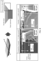
- FIG. 4 shows a configuration of a production device for use in the vapor phase growth step (A) (Group III element nitride crystal production device using vapor deposition).
- A Group III element nitride crystal production device using vapor deposition
- the present production device 100 includes a first container 101, a second container 102, and a substrate support 103, and the second container 102 and the substrate support 103 are disposed inside the first container 101.
- the second container 102 is fixed on the left side surface of the first container 101 in FIG. 4 .
- the substrate support 103 is fixed on the lower surface of the first container 101.
- the second container 102 includes a Group III metal placement portion 104 on its lower surface.
- the second container 102 includes an oxidizing gas introduction tube 105 on its left side surface and a Group III metal oxidization product gas delivery tube 106 on its right side surface in FIG. 4 .
- An oxidizing gas can be continuously introduced (supplied) into the second container 102 through the oxidizing gas introduction tube 105.
- the first container 101 includes nitrogen-containing gas introduction tubes 107a and 107b on its left side surface and an exhaust tube 108 on its right side surface in FIG. 4 .
- a nitrogen-containing gas can be continuously introduced (supplied) into the first container 101 through the nitrogen-containing gas introduction tubes 107a and 107b.
- First heating units 109a and 109b and second heating units 200a and 200b are further disposed outside the first container.
- the production device for use in the production method of the present invention is by no means limited thereto.
- only one second container 102 is disposed inside the first container 101.
- a plurality of second containers 102 may be disposed inside the first container 101.
- the present production device includes only one oxidizing gas introduction tube 105 and may however include a plurality of oxidizing gas introduction tubes 105.
- the production device 100 of FIG. 4 is described above as the production device for use in the vapor phase growth step (A) and can be used in the vapor phase growth step (B) as mentioned below.
- the generated Group III metal oxidization product gas 111a is delivered to the outside of the second container 102 (or 301) through the Group III metal oxidization product gas delivery tube 106 (Group III metal oxidization product gas 111b).
- the Group III metal oxidization product gas 111b is Ga 2 O in FIG. 7 and, however, is by no means limited thereto.
- a first carrier gas may be introduced to deliver the Group III metal oxidization product gas 111b to the outside of the second container 102 (301) through the Group III metal oxidization product gas delivery tube 106.
- the first carrier gas may be the same as the inactive gas, for example.
- the flow rate (partial pressure) of the first carrier gas may be the same as that of the inactive gas.
- the inactive gas may be used as the first carrier gas.
- the temperature of the substrate is not limited to particular temperatures and is preferably 1200°C or more, more preferably 1300°C or more, yet more preferably 1400°C or more, particularly preferably 1500°C or more to maintain the crystal generation rate and improve crystalline properties.
- the upper limit of the temperature of the substrate is not limited to particular temperatures and is, for example, 2000°C or less.
- a second carrier gas may be introduced to transfer the introduced nitrogen-containing gas to a crystal generation region (to the vicinity of the substrate support 103 in the first container 101 in FIGs. 4 to 7 ).
- the carrier gas may be introduced through a carrier gas introduction tube (not shown) provided separately from the nitrogen-containing gas introduction tube or may be introduced through the nitrogen-containing gas introduction tube after mixing with the nitrogen-containing gas.
- the same gas as the first carrier gas can be used as the second carrier gas, for example.
- the flow rate of the second carrier gas can be set, as appropriate, according to the flow rate of the nitrogen-containing gas, for example.
- the flow rate of the second carrier gas is, for example, in the range from 0.01 to 1500 Pa•m 3 /s, preferably from 0.08 to 600 P•am 3 /s, more preferably from 0.15 to 300 Pa•m 3 /s.
- the mixing ratio A: B (volume ratio) between the nitrogen-containing gas (A) and the second carrier gas (B) is not limited to particular ratios and is preferably in the range from 2 : 98 to 80 : 20, more preferably from 5 : 95 to 60 : 40, yet more preferably from 10 : 90 to 40 : 60.
- the mixing ratio A: B (volume ratio) can be set by, for example, a method in which the mixed gas is previously produced at a predetermined mixing ratio or a method in which the flow rates (partial pressures) of the nitrogen-containing gas and the second carrier gas are adjusted.
- the Group III element nitride crystal (e.g., GaN crystal) generation step can be performed preferably under pressure.
- the pressure in the pressurization is as mentioned above.
- the pressurization can be, for example, pressurization with the nitrogen-containing gas, the second carrier gas, or the like.
- the Group III element nitride crystal generation step may be performed in an atmosphere of a dopant-containing gas.
- a dopant-containing GaN crystal can be generated.
- the dopant include Si, S, Se, Te, Ge, Fe, Mg, and Zn.
- the dopants may be used alone or in a combination of two or more of them.
- Examples of the dopant-containing gas include monosilane (SiH 4 ), disilane (Si 2 H 6 ), triethylsilane (SiH(C 2 H 5 ) 3 ), tetraethylsilane (Si(C 2 H 5 ) 4 ), H 2 S, H 2 Se, H 2 Te, GeH 4 , Ge 2 O, SiO, MgO, and ZnO, and they may be used alone or in a combination of two or more of them.
- the dopant-containing gas may be introduced through a dopant-containing gas introduction tube (not shown) provided separately from the nitrogen-containing gas introduction tube or may be introduced through the nitrogen-containing gas introduction tube after mixing with the nitrogen-containing gas.
- the dopant-containing gas may be introduced after mixing with the second carrier gas.
- the generation rate of the Group III element nitride crystal is not limited to particular rates and is, for example, 100 ⁇ m/h or more, preferably 500 ⁇ m/h or more, and more preferably 1000 ⁇ m/h or more.
- the vapor phase growth step (A) can be performed as described above and, however, is by no means limited thereto.
- the reaction is performed preferably in the presence of a reducing gas in a reaction system in the vapor phase growth step (A).
- the reaction is performed more preferably through mixing the reducing gas with at least one of the oxidizing gas or the nitrogen-containing gas. That is, in FIG. 5 or 7 , the reducing gas may be mixed with at least one of the nitrogen-containing gases 203a and 203b and the oxidizing gas 201a (or 401a).
- the reducing gas is yet more preferably mixed with the oxidizing gas.
- reaction efficiency of the Group III metal oxidization product gas reaction efficiency of the Group III metal oxidization product gas
- H 2 gas the reducing gas
- H 2 O gas the oxidizing gas
- Examples of the reducing gas for use in the vapor phase growth step (A) include hydrogen gas, carbon monoxide gas, a hydrocarbon gas such as methane gas or ethane gas, hydrogen sulfide gas, and sulfur dioxide, and they may be used alone or in a combination of two or more of them.
- hydrogen gas is particularly preferable. The higher the purity of the hydrogen gas is, the better. The purity of the hydrogen gas is particularly preferably 99.9999% or more.
- the reaction temperature in the Group III metal oxidization product gas generation step performed in the presence of a reducing gas is not limited to particular temperatures and is preferably 900°C or more, more preferably 1000°C or more, yet more preferably 1100°C or more to prevent the generation of byproduct.
- the upper limit of the reaction temperature is not limited to particular temperatures and is, for example, 1500°C or less.
- the amount of the reducing gas to be used in the vapor phase growth step (A) is not limited to particular amounts, and the proportion of the reducing gas in the total volume of the oxidizing gas and the reducing gas is, for example, from 1 to 99 vol%, preferably from 3 to 80 vol%, more preferably from 5 to 70 vol%.
- the flow rate of the reducing gas can be set, as appropriate, according to, for example, the flow rate of the oxidizing gas.
- the flow rate of the reducing gas is not limited to particular rates and is, for example, in the range from 0.001 to 1000 Pa•m 3 /s, preferably from 0.005 to 500 Pa•m 3 /s, more preferably from 0.01 to 100 Pa•m 3 /s.
- the Group III metal oxidization product gas111a (111b) is generated preferably under pressure as mentioned above, and the pressure is, for example, as mentioned above.
- the pressurization may be, for example, pressurization with the oxidizing gas or the reducing gas.
- the vapor phase growth step (A) in the present invention is vapor deposition and however can be performed without using a halide as a raw material.
- a Group III element nitride crystal can be produced without producing a byproduct containing halogen in contrast to the halide vapor phase epitaxy described in JP S52-23600 A (Patent Document 1) or the like. Accordingly, for example, the influences of clogging of an exhaust tube of the production device with the byproduct containing halogen (e.g., NH 4 Cl) and the like on the generation of the crystal can be prevented.
- the vapor phase growth step (B) can be performed using the production device 100 shown in FIG. 4 .
- a Group III metal placement portion 104 is used as a Group III element oxide placement portion 104
- the oxidizing gas introduction tube 105 is used as a reducing gas introduction tube 105
- the Group III metal oxidization product gas delivery tube 106 is used as a reduced product gas delivery tube 106.
- the vapor phase growth step (B) includes a reduced product gas generation step and a crystal generation step.
- the introduced hydrogen gas 201b reacts with the Ga 2 O 3 to generate a Ga 2 O 3 gas (following formula (III)).
- the generated Ga 2 O gas 111a is delivered to the outside of the second container 102 through the reduced product gas delivery tube 106 as a Ga 2 O gas 111b.
- the delivered Ga 2 O gas 111b reacts with the introduced ammonia gas 203c.
- a GaN crystal 204 is thus generated on the Group III element nitride seed crystal disposed on the substrate 202 (the following formula (IV)).
- the vapor phase growth step (B) is advantageous in terms of cost because a filter for removing byproducts is not required.
- the vapor phase growth step (B), however, is by no means limited thereto.
- a ternary or higher nitride crystal is, generated on the substrate, for example.
- the ternary or higher nitride crystal can be, for example, Ga x In 1-x N (0 ⁇ x ⁇ 1).
- the amount of the Ga 2 O gas to be supplied is, for example, in the range from 5 ⁇ 10 -5 to 5 ⁇ 10 1 mol/h, preferably, from 1 ⁇ 10 -4 to 1 ⁇ 10 1 mol/h, more preferably from 2 ⁇ 10 -4 to 2 mol/h.
- the amount of the Ga 2 O gas to be supplied can be adjusted by, for example, adjusting the flow rate (partial pressure) of the first carrier gas in generation of the Ga 2 O gas.
- the flow rate (partial pressure) of the ammonia gas can be set, as appropriate, according to conditions such as the temperature of the substrate.
- the partial pressure of the ammonia gas is not limited to particular pressures and is, for example, in the range from 0.2 to 3000 kPa, preferably from 0.5 to 2000 kPa, more preferably from 1.5 to 500 kPa.
- a second carrier gas may be introduced to transfer the introduced ammonia gas to a crystal generation region.
- the second carrier gas may be introduced through a carrier gas introduction tube (not shown) provided separately from the nitrogen-containing gas introduction tube or may be introduced through the nitrogen-containing gas introduction tube after mixing with the ammonia gas.
- the same gas as the first carrier gas can be used as the second carrier gas, for example.
- the flow rate (partial pressure) of the second carrier gas can be set, as appropriate, according to the flow rate (partial pressure) of the nitrogen-containing gas.
- the flow rate of the second carrier gas is not limited to particular pressures and is, for example, in the range from 0.2 to 3000 Pa•m 3 /s, preferably from 0.5 to 2000 P•am 3 /s, more preferably from 1.5 to 1000 Pa•m 3 /s.
- the GaN crystal is generated preferably under pressure.
- the pressure in the pressurization is as mentioned above.
- the pressurization can be, for example, pressurization with the ammonia gas, the second carrier gas, or the like.
- the GaN crystal may be generated in an atmosphere of a dopant-containing gas. In such atmosphere, a dopant-containing GaN crystal can be generated.
- the dopant include Si, S, Se, Te, Ge, Fe, Mg, and Zn.
- the dopants may be used alone or in a combination of two or more of them.
- Examples of the dopant-containing gas include monosilane (SiH 4 ), disilane (Si 2 H 6 ), triethylsilane (SiH(C 2 H 5 ) 3 ), tetraethylsilane (Si(C 2 H 5 ) 4 ), H 2 S, H 2 Se, H 2 Te, GeH 4 , Ge 2 O, SiO, MgO, and ZnO, and they may be used alone or in a combination of two or more of them.
- the dopant-containing gas may be introduced through a dopant-containing gas introduction tube (not shown) provided separately from the nitrogen-containing gas introduction tube or may be introduced through the nitrogen-containing gas introduction tube after mixing with the ammonia gas.
- the dopant-containing gas may be introduced after mixing with the second carrier gas.
- the concentration of the dopant in the dopant-containing gas is not limited to particular concentrations and is, for example, in the range from 0.001 to 100000 ppm, preferably from 0.01 to 1000 ppm, more preferably from 0.1 to 10 ppm.
- the generation rate of the GaN crystal is not limited to particular rates and is not limited to particular rates and is, for example, 100 ⁇ m/h or more, preferably 500 ⁇ m/h or more, and more preferably 1000 ⁇ m/h or more.
- the size of the Group III element nitride crystal to be produced by the vapor phase growth step is not limited to particular sizes, and the major axis is preferably 15 cm (about 6 inches) or more, more preferably 20 cm (about 8 inches) or more, particularly preferably 25 cm (about 10 inches) or more.
- the height of the Group III element nitride crystal is not limited to particular heights and may be, for example 1 cm or more, preferably 5 cm or more, more preferably 10 cm or more.
- the production method of the present invention is not limited by the production of such large Group III element nitride crystal and can be used to produce a higher-quality Group III element nitride crystal in a conventional size, for example.
- the height (thickness) of the Group III element nitride crystal is not limited to p articular thicknesses as mentioned above and may be, for example, less than 1600 ⁇ m.
- the dislocation density is not limited to particular densities and is preferably 1.0 ⁇ 10 7 cm -2 or less, more preferably 1.0 ⁇ 10 5 cm -2 or less, yet more preferably 1.0 ⁇ 10 4 cm -2 or less, yet more preferably 1.0 ⁇ 10 3 cm -2 or less, yet more preferably 1.0 ⁇ 10 2 cm -2 or less.
- the dislocation density is ideally 0. However, it is generally impossible for the dislocation density to be 0.
- the dislocation density is thus, for example, more than 0 and is particularly preferably a measurement limit or less of a measurement device.
- the dislocation density may be expressed as, for example, an average of the dislocation densities of the entire crystal, and more preferably, the maximum value in the crystal is the above-described values or less.
- the half width of each of a symmetric reflection component (002) and an asymmetric reflection component (102) by XRC is, for example, 300 seconds or less, preferably 100 seconds or less, more preferably 30 seconds or less, ideally 0.
- the production method of the present invention may further include a crystal re-growth step of further growing the produced Group III element nitride crystal.
- the produced Group III element nitride crystal is cut so that any plane (e.g., c-, m-, or a-plane or another nonpolar plane) is exposed, and the Group III element nitride crystal is further grown using the plane as a crystal growth plane.
- any plane e.g., c-, m-, or a-plane or another nonpolar plane
- a Group III element nitride crystal with a large area of any plane and a large thickness can be produced thereby.
- the Group III element nitride crystal produced by the production method of the present invention is, for example, a high-quality, large Group III element nitride crystal with few defects.
- the quality is not particularly limited, the dislocation density is, for example, preferably in the numerical range described in the section "1.
- Method for producing Group III element nitride crystal The size of the Group III element nitride crystal also is not limited to p articular sizes and is, for example, as mentioned above.
- the use of the Group III element nitride crystal is not particularly limited and can be used in a semiconductor device because of having properties of a semiconductor, for example.
- a laser diode (LD) that emits blue light is applied to high-density optical discs and displays, and a light-emitting diode (LED) that emits blue light is applied to displays and lighting.
- an ultraviolet LD is expected to be applied to biotechnology, and an ultraviolet LED is expected to be an ultraviolet source as a substitute for a mercury lamp.
- an inverter using a Group III-V compound as a power semiconductor for inverter can be used for, for example, electric power generation such as a solar cell.
- the Group III element nitride crystal is by no means limited thereto and is applicable to any other semiconductor devices and a wide of other technical fields.
- GaN crystals were produced by vapor deposition as described below.
- the cross sections of the Group III element nitride crystals were subjected to a Scanning Electron Microscope (SEM) observation using a scanning electron microscope (produced by KEYENCE CORPORATION, trade name:"VHX-D500"). Each half width was measured by XRC using Smartlab (trade name) produced by RIGAKU.
- a GaN crystal was grown on each of the +c-plane and the -c-plane, and results were compared on the basis of whether the diameters were increasing with growing of the crystal.
- a 2-inch free-standing substrate produced by FKK Corporation was used as a seed crystal for use in the vapor phase growth step.
- This free-standing substrate is formed of a GaN crystal produced by HVPE (vapor deposition) and also serves as a GaN seed crystal.
- a GaN crystal was grown, by vapor deposition, on the crystal growth plane (the +c-plane or the -c-plane) of the seed crystal produced by liquid deposition, using a device having the configuration of FIG. 4 to produce an intended GaN crystal.
- the GaN crystal produced using a +c-plane as a crystal growth plane is of Comparative Example 1
- the GaN crystal produced using a -c-plane as a crystal growth plane is of Example 1.
- a quartz container was used as a second container 102.
- the inner diameter of each of an oxidizing gas introduction tube 105 and nitrogen-containing gas introduction tubes 107a and 107b was 4 mm.
- the vapor deposition (vapor phase growth step) was performed as follows. That is, in the present example, a large excess amount of gallium(III) oxide (Ga 2 O 3 ) powder (purity: 99.9%) was used as a Group III element-containing raw material 110. A hydrogen gas (H 2 ) was used as a reducing gas 201a. The partial pressure of the hydrogen gas (H2) was set to be 3.3 kPa. The hydrogen gas 201a (201b) reacted with the gallium(III) oxide 110 to generate a gallium(I) oxide (Ga 2 O) gas 111a (111b). In the present example, the partial pressure of the gallium(I) oxide gas 111a (111b) was assumed to be 4.3 kPa.
- the conversion efficiency from Ga 2 O 3 to Ga 2 O (gallium(I) oxide) was then assumed to be 100% (i.e., it was assumed that 100% of the reduced weight of Ga 2 O 3 was converted into Ga 2 O), and the partial pressure of the gallium(I) oxide 111a (111b) was calculated as 4.3 kPa as described above.
- ammonia gas (NH 3 ) was used as nitrogen-containing gases 203a and 203b.
- the partial pressure of the ammonia gas was set to be 10 kPa.
- NH 3 gas (100% NH 3 gas containing no other gases) was introduced as a carrier gas through the oxidizing gas introduction tube 105 and the nitrogen-containing gas introduction tubes 107a and 107b, and pressurization was performed so that the total pressure became 100 kPa.
- the temperature of the Group III element-containing raw material (Ga 2 O 3 ) 110 was set to be 900°C.
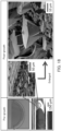
- FIG. 8 Images of the cross sections of outer peripheries at the upper ends of the respective produced GaN crystals were thereafter taken by SEM as shown in FIG. 8 . If the diameter is increasing toward the top of the GaN crystal, the diameter is increasing with growing of the crystal.
- a left photograph in FIG. 8 is a cross-sectional SEM image of the GaN crystal (Comparative Example 1) produced using a +c-plane as a crystal growth plane.
- a right photograph in FIG. 8 is a cross-sectional SEM image of the GaN crystal (Example 1) produced using a -c-plane as a crystal growth plane.
- an increase in diameter was not found in the GaN crystal of Comparative Example 1, whereas the increase in diameter was found in the GaN crystal of Example 1.
- the GaN crystal was produced on a -c-plane to check for an increase in diameter of a GaN crystal growth for a long period of time (crystal growth).
- the GaN crystal was produced in the same manner as in Example 1 except that the conditions of the vapor phase growth step were as follows.
- the "temperature of growing portion” refers to the temperature of a GaN crystal layer substrate 202 and means the same as the crystal growth temperature.
- the "temperature of raw material portion” refers to the temperature of a Group III element-containing raw material (Ga 2 O 3 ) 110.
- the “growing time” means the same as the crystal growth time (time in which each gas is caused to flow) described in Example 1.
- each GaN crystal for the growing time of 60 minutes (Example 2-1), 120 minutes (Example 2-2), or 180 minutes (Example 2-3) was produced as follows.
- the "NH 3 line” shows flow rates of the nitrogen containing gasses 203a and 203b (NH 3 in the present example) and the carrier gas (NH 3 in the present example) caused to flow through the nitrogen-containing gas introduction tubes107a and 107b.
- the "Ga 2 O line” shows flow rates of the gas 201a of the reduced product (H2 in the present example) and the carrier gas (NH 3 in the present example) caused to flow through the oxidizing gas introduction tube 105.
- the "diameter ⁇ of raw material tube” shows the inner diameter of an oxidizing gas introduction tube 106. The same applies hereinafter.
- FIGs. 9 and 10 show the cross-sectional SEM images. As shown in FIGs. 9 and 10 , a habit (crystal habit) of increasing a diameter was observed in the growth for a long period of time of the present example (Example 2) as in Example 1.
- FIG. 11 is a graph showing a correlation between the thickness of the GaN crystal produced in the present example (Example 2) and the growth of the GaN crystal in the horizontal direction.
- the horizontal axis represents a dimensional increase [ ⁇ m] of the produced GaN crystal in the horizontal direction, which represents the extent of the growth of the GaN crystal in the horizontal direction. That is, in the present example, images of the cross section of an outer periphery at the top of the produced GaN crystal were taken by SEM as shown in the drawing on the upper right side of FIG. 8 or 9 , the horizontal axis of the graph of FIG.
- the thickness does not include the thickness of the GaN seed crystal (free-standing substrate).
- the thickness was increasing, and the GaN crystal in the horizontal direction was growing further as an increase in growing time. That is, a positive correlation between the thickness and the growth in the horizontal direction was observed. This demonstrates that the diameter of the GaN crystal can be increased by the crystal growth for a long period of time.
- the crystal growth plane was determined (whether the crystal growth plane was a -c-plane or a +c-plane was determined) by etching to check the presence or absence of a polarity-inverted region in the crystal growth plane of the GaN crystal (after growth for 60 minutes) produced in Example 2.
- the conditions of the etching are as follows, and the upper surface (crystal growth plane) of the GaN crystal was etched.
- FIG. 12 shows the respective post-etching bird's-eye SEM images (microscope photographs) of a -c-plane and a +c-plane of the GaN seed crystal (free-standing GaN substrate produced by FKK) for reference.
- the left photograph of FIG. 12 is a photograph of the -c-plane of the GaN seed crystal after the etching
- the right photograph of FIG. 12 is a photograph of the +c-plane of the GaN seed crystal after the etching.
- the conditions of the etching are as described above.
- the -c-plane after the etching includes surfaces tilted with respect to the -c-plane, i.e., includes fine asperities.
- GaN was produced at different partial pressures of the Ga 2 O gas to check a relationship between the degree of supersaturation of a Ga 2 O gas and the growth of the GaN crystal. That is, a GaN crystal was produced in the same manner as in Example 1 except that the conditions of the vapor phase growth step was the following condition (1) or (2).
- the condition (1) corresponds to Example 3-1
- the following condition (2) corresponds to Example 3-2.
- the partial pressure of the Ga 2 O gas in the vapor phase growth step performed under the following condition (1) was 19.4 Pa
- that in the vapor phase growth step performed under the following condition (2) was 3.21 Pa.
- a method for calculating (assuming) the partial pressure of the Ga 2 O gas was the same as in Example 1.
- a GaN crystal was produced in the same manner as in the present example (Example 6) except that the +c-plane was used as the crystal growth plane, and the vapor phase growth step was performed under the following conditions (Comparative Example 2).
- the "seed crystal diameter ⁇ " and the "pitch” mean the same as in Example 6.
Landscapes
- Chemical & Material Sciences (AREA)
- Engineering & Computer Science (AREA)
- Materials Engineering (AREA)
- Metallurgy (AREA)
- Organic Chemistry (AREA)
- Crystallography & Structural Chemistry (AREA)
- Chemical Kinetics & Catalysis (AREA)
- General Chemical & Material Sciences (AREA)
- Inorganic Chemistry (AREA)
- Mechanical Engineering (AREA)
- Crystals, And After-Treatments Of Crystals (AREA)
- Chemical Vapour Deposition (AREA)
Claims (15)
- Verfahren zur Herstellung eines Kristalls aus einem Nitrid eines Elements der Gruppe III, wobei das Verfahren umfasst:einen Schritt des Wachsens aus der Dampfphase, in dem ein Kristall aus einem Nitrid des Elements der Gruppe III auf einer Kristallwachstumsebene eines Keimkristalls aus einem Nitrid des Elements der Gruppe III durch Dampfabscheidung gezüchtet wird, wobeidie Kristallwachstumsebene eine Ebene auf einer -c-Ebene-Seite ist,eine Kristallwachstumstemperatur 1200 °C oder mehr beträgt, undin dem Schritt des Wachsens aus der Dampfphase der Kristall aus einem Nitrid des Elements der Gruppe III in einer Wachstumsrichtung gezüchtet wird, wobei ein Winkel, der zwischen der Wachstumsrichtung und der -c-Richtung gebildet wird, 10° oder weniger beträgt, und wobei:
der Schritt des Wachsens aus der Dampfphase ein Schritt ist, bei dem ein Metall der Gruppe III, ein Oxidationsmittel, das eine sauerstoffhaltige Verbindung ist, und ein stickstoffhaltiges Gas miteinander zur Reaktion gebracht werden, um den Kristall aus einem Nitrid des Elements der Gruppe III zu züchten. - Verfahren nach Anspruch 1, wobei:(A) das Metall der Gruppe III mindestens eines aus der Gruppe bestehend aus Gallium, Indium und Aluminium ist;
und/oder(B) der Schritt des Wachsens aus der Dampfphase umfasst:einen Schritt zum Erzeugen eines Oxidationsproduktgases des Metalls der Gruppe III, in dem das Metall der Gruppe III und das Oxidationsmittel miteinander zur Reaktion gebracht werden, um ein Oxidationsproduktgas des Metalls der Gruppe III zu erzeugen; undeinen Schritt zum Erzeugen eines Kristalls aus einem Nitrid des Elements der Gruppe III, bei dem das Oxidationsproduktgas des Metalls der Gruppe III und das stickstoffhaltige Gas miteinander zur Reaktion gebracht werden, um den Kristall aus einem Nitrid des Elements der Gruppe III zu erzeugen. - Verfahren nach Anspruch 2, wobei
der Schritt des Wachsens aus der Dampfphase umfasst:einen Schritt zum Erzeugen eines Oxidationsproduktgases des Metalls der Gruppe III, bei dem das Metall der Gruppe III und das Oxidationsmittel miteinander zur Reaktion gebracht werden, um ein Oxidationsproduktgas des Metalls der Gruppe III zu erzeugen; undeinen Schritt zum Erzeugen eines Kristalls aus einem Nitrid des Elements der Gruppe III, bei dem das Oxidationsproduktgas des Metalls der Gruppe III und das stickstoffhaltige Gas miteinander zur Reaktion gebracht werden, um den Kristall aus einem Nitrid des Elements der Gruppe III zu erzeugen, und wobei:(A) in dem Schritt zum Erzeugen des Oxidationsproduktgases des Metalls der Gruppe III das Metall der Gruppe III unter Erhitzen mit dem Oxidationsmittel zur Reaktion gebracht wird;
und/oder(B) das Oxidationsproduktgas des Metalls der Gruppe III ein Metalloxidgas der Gruppe III ist, wobei das Metall der Gruppe III optional Gallium ist und das Metalloxidgas der Gruppe III optional ein Ga2O-Gas ist. - Verfahren nach einem der Ansprüche 1 bis 3, wobei(A) das Oxidationsmittel ein oxidierendes Gas ist, das mindestens eines ausgewählt aus der Gruppe bestehend aus einem H2O-Gas, einem O2-Gas, einem CO2-Gas und einem CO-Gas ist, und optional der Anteil des Volumens des oxidierenden Gases am Gesamtvolumen des oxidierenden Gases und des stickstoffhaltigen Gases im Bereich von 0,001 % bis 60 % liegt;
und/oder(B) das stickstoffhaltige Gas mindestens eines ausgewählt aus der Gruppe bestehend aus N2, NH3 einem Hydrazingas und einem Alkylamingas ist; und/oder(C) in dem Schritt des Wachsens aus der Dampfphase die Reaktion unter Vorhandensein eines Reduktionsgases in einem Reaktionssystem durchgeführt wird, wobei optional: (i) das Reduktionsgas ein wasserstoffhaltiges Gas oder mindestens eines ausgewählt aus der Gruppe bestehend aus einem H2-Gas, einem Kohlenmonoxid(CO)-Gas, einem Kohlenwasserstoffgas, einem H2S-Gas, einem SO2-Gas und einem NH3-Gas ist, in dem das Kohlenwasserstoffgas optional mindestens eines von einem Methangas oder einem Ethangas ist; und/oder (ii) das Oxidationsmittel ein oxidierendes Gas ist, das mindestens eines ausgewählt aus der Gruppe bestehend aus einem H2O-Gas, einem O2-Gas, einem CO2-Gas und einem CO-Gas ist, und das Reduktionsgas mit dem oxidierenden Gas gemischt wird; und/oder (iii) das Reduktionsgas mit dem stickstoffhaltigen Gas gemischt wird; und/oder (iv) die Reaktion unter Vorhandensein eines Reduktionsgases bei 650 °C oder mehr durchgeführt wird; und/oder(D) in dem Schritt des Wachsens aus der Dampfphase der Kristall aus einem Nitrid des Elements der Gruppe III unter Druck erzeugt wird. - Verfahren zur Herstellung eines Kristalls aus einem Nitrid eines Elements der Gruppe III, wobei das Verfahren umfasst:einen Schritt des Wachsens aus der Dampfphase, bei dem ein Kristall aus einem Nitrid des Elements der Gruppe III auf einer Kristallwachstumsebene eines Keimkristalls aus einem Nitrid des Elements der Gruppe III durch Dampfabscheidung gezüchtet wird, wobeidie Kristallwachstumsebene eine Ebene auf einer -c-Ebene ist,eine Kristallwachstumstemperatur 1200 °C oder mehr beträgt, undin dem Schritt des Wachsens aus der Dampfphase der Kristall aus einem Nitrid des Elements der Gruppe III in einer Wachstumsrichtung gezüchtet wird, wobei ein Winkel, der zwischen der Wachstumsrichtung und der -c-Richtung gebildet wird, 10° oder weniger beträgt, und wobei:
der Schritt des Wachsens aus der Dampfphase umfasst: einen Schritt zur Erzeugung eines reduzierten Produktgases, bei dem ein Elementoxid der Gruppe III und ein Reduktiongas miteinander zur Reaktion gebracht werden, um ein Gas eines reduzierten Produkts des Elementoxids der Gruppe III zu erzeugen; und einen Kristallerzeugungsschritt, bei dem das Gas des reduzierten Produkts und ein stickstoffhaltiges Gas miteinander zur Reaktion gebracht werden, um den Kristall aus einem Nitrid des Elements der Gruppe III zu erzeugen. - Verfahren nach Anspruch 5, wobei
in dem Schritt zum Erzeugen des reduzierten Produktgases das Elementoxid der Gruppe III unter Erhitzen mit dem Reduktionsgas zur Reaktion gebracht wird. - Verfahren nach einem der Ansprüche 1, 2 und 6, wobei(A) das Elementoxid der Gruppe III Ga2O3 ist,das Gas des reduzierten Produkts Ga2O-Gas ist undder Kristall aus einem Nitrid des Elements der Gruppe III ein GaN-Kristall ist;und/oder(B) der Schritt zum Erzeugen des reduzierten Produktgases in einer Atmosphäre eines Gasgemisches aus dem Reduktionsgas und einem inaktiven Gas durchgeführt wird, wobei optional: (i) der Anteil des Reduktionsgases an der Gesamtmenge des Gasgemisches 3 Vol.-% oder mehr bis weniger als 100 Vol.-% beträgt und der Anteil des inaktiven Gases an der Gesamtmenge des Gasgemisches mehr als 0 bis 97 Vol.-% oder weniger beträgt; und/oder (ii) das inaktive Gas Stickstoffgas umfasst; und/oder(C) das Reduktionsgas ein Wasserstoffgas umfasst; und/oder(D) das stickstoffhaltige Gas ein Ammoniakgas umfasst; und/oder(E) der Kristallerzeugungsschritt unter Druck durchgeführt wird.
- Verfahren nach einem der Ansprüche 1 bis 7, wobei:(A) die Kristallwachstumsebene des Keimkristalls aus dem Nitrid des Elements der Gruppe III(i) parallel zu einer -c-Ebene ist oder(ii) in einem Zustand ist, in dem ein Winkel, der zwischen der Kristallwachstumsebene und der -c Ebene gebildet wird, 10° oder weniger beträgt; und/oder(B) die Kristallwachstumsebene des Keimkristalls aus dem Nitrid des Elements der Gruppe III eine unebene Ebene ist.
- Verfahren nach einem der Ansprüche 1 bis 8, ferner umfassend:
einen Schneideschritt, bei dem der Kristall aus einem Nitrid des Elements der Gruppe III geschnitten wird, um mindestens ein Kristallsubstrat aus einem Nitrid des Elements der Gruppe III zu schneiden, wobei optional das mindestens eine Kristallsubstrat aus einem Nitrid des Elements der Gruppe III, das im Schneideschritt geschnitten wird, als Keimkristall eines Nitrids des Elements der Gruppe III im Schritt des Wachsens aus der Dampfphase verwendet wird, wobei optional der Schneideschritt und der Schritt des Wachsens aus der Dampfphase, der das mindestens eine im Schneideschritt herausgeschnittene Kristallsubstrat eines Nitrids des Elements der Gruppe III als Keimkristall eines Nitrids des Elements der Gruppe III verwendet, wiederholt durchgeführt werden. - Verfahren nach einem der Ansprüche 1 bis 9, wobei:(A) der herzustellende Kristall aus einem Nitrid des Elements der Gruppe III durch AlxGayIn1-x-yN (0 ≤ x ≤ 1,0 ≤ y ≤ 1, x + y ≤ 1) dargestellt wird; oder(B) der herzustellende Kristall aus einem Nitrid des Elements der Gruppe III GaN ist.
- Verfahren nach einem der Ansprüche 1 bis 10, wobei:(A) der herzustellende Kristall aus einem Nitrid eines Elements der Gruppe III eine Hauptachse von 15 cm oder mehr aufweist; und/oder(B) der herzustellende Kristall aus einem Nitrid des Elements der Gruppe III eine Versetzungsdichte von 1,0 x 107 cm-2 oder weniger aufweist; und/oder(C) in dem herzustellenden Kristall aus einem Nitrid des Elements der Gruppe III eine halbe Breite jeder einer symmetrischen Reflexionskomponente (002) und einer asymmetrischen Reflexionskomponente (102) durch eine Röntgen-Rocking-Curve-Analyse (XRC) 300 Sekunden oder weniger beträgt; und/oder(D) der herzustellende Kristall aus einem Nitrid des Elements der Gruppe III eine Sauerstoffkonzentration von 1 × 1020 cm-3 oder weniger aufweist.
- Verfahren nach einem der Ansprüche 1 bis 11, wobei
der Keimkristall aus einem Nitrid eines Elements der Gruppe III durch Flüssigkeitsabscheidung hergestellt wird. - Verfahren nach einem der Ansprüche 1 bis 12, wobei der Kristall aus einem Nitrid eines Elements der Gruppe III ein Halbleiter ist.
- Verfahren zur Herstellung einer Halbleitervorrichtung, die einen Kristall aus einem Nitrid eines Elements der Gruppe III umfasst, wobei das Verfahren umfasstHerstellen eines Kristalls aus einem Nitrid des Elements der Gruppe III durch das Verfahren nach einem der Ansprüche 1 bis 12, wobeider Kristall aus einem Nitrid des Elements der Gruppe III ein Halbleiter ist.
- Verwendung einer Vorrichtung zur Herstellung eines Kristalls aus einem Nitrid eines Elements der Gruppe III in dem Verfahren nach einem der Ansprüche 1 bis 12, wobei:(A) die Vorrichtung umfassteine Dampfphasenwachstumseinheit, die so konfiguriert ist, dass sie einen Kristall aus einem Nitrid des Elements der Gruppe III auf einem Keimkristall aus einem Nitrid des Elements der Gruppe III durch Dampfabscheidung züchtet; undeine Flüssigrohstoffzufuhreinheit, die so konfiguriert ist, dass sie der Dampfphasenwachstumseinheit kontinuierlich Galliummetall in flüssiger Form zuführt; oder(B) der Schritt des Wachsens aus der Dampfphase in dem Verfahren ein Schritt ist, bei dem Galliummetall in flüssiger Form, ein Oxidationsmittel, das eine sauerstoffhaltige Verbindung ist, und ein stickstoffhaltiges Gas miteinander zur Reaktion gebracht werden, um den Kristall aus einem Nitrid des Elements der Gruppe III zu züchten,die Vorrichtung zur Herstellung des Kristalls aus einem Nitrid des Elements der Gruppe III umfasst:einen Reaktionsbehälter;eine Galliummetallzufuhreinheit;eine Oxidationsmittelzufuhreinheit; undeine Zufuhreinheit für stickstoffhaltiges Gas,die Galliummetallzufuhreinheit in der Lage ist, das Galliummetall kontinuierlich dem Reaktionsbehälter zuzuführen,die Oxidationsmittelzufuhreinheit in der Lage ist, das Oxidationsmittel kontinuierlich dem Reaktionsbehälter zuzuführen,die Zufuhreinheit für stickstoffhaltiges Gas in der Lage ist, das stickstoffhaltige Gas kontinuierlich dem Reaktionsbehälter zuzuführen, unddas Galliummetall, das Oxidationsmittel und das stickstoffhaltige Gas im Reaktionsbehälter miteinander zur Reaktion gebracht werden, um den Kristall aus einem Nitrid des Elements der Gruppe III herzustellen.
Applications Claiming Priority (2)
| Application Number | Priority Date | Filing Date | Title |
|---|---|---|---|
| JP2014220681 | 2014-10-29 | ||
| PCT/JP2015/080363 WO2016068181A1 (ja) | 2014-10-29 | 2015-10-28 | Iii族元素窒化物結晶製造方法、iii族元素窒化物結晶、半導体装置、半導体装置の製造方法およびiii族元素窒化物結晶製造装置 |
Publications (3)
| Publication Number | Publication Date |
|---|---|
| EP3199670A1 EP3199670A1 (de) | 2017-08-02 |
| EP3199670A4 EP3199670A4 (de) | 2018-05-09 |
| EP3199670B1 true EP3199670B1 (de) | 2025-06-25 |
Family
ID=55857516
Family Applications (1)
| Application Number | Title | Priority Date | Filing Date |
|---|---|---|---|
| EP15855510.2A Active EP3199670B1 (de) | 2014-10-29 | 2015-10-28 | Verfahren zur herstellung eines gruppe-iii-nitrid-kristalls, verfahren zur herstellung eines halbleiterbauelements und verwendung einer vorrichtung zur herstellung des gruppe-iii-nitrid-kristalls |
Country Status (4)
| Country | Link |
|---|---|
| US (1) | US10011921B2 (de) |
| EP (1) | EP3199670B1 (de) |
| JP (1) | JP6596692B2 (de) |
| WO (1) | WO2016068181A1 (de) |
Families Citing this family (3)
| Publication number | Priority date | Publication date | Assignee | Title |
|---|---|---|---|---|
| US10475930B2 (en) | 2016-08-17 | 2019-11-12 | Samsung Electronics Co., Ltd. | Method of forming crystalline oxides on III-V materials |
| JP7228185B2 (ja) | 2019-02-04 | 2023-02-24 | 国立大学法人大阪大学 | Iii族窒化物結晶の製造方法 |
| JP7685358B2 (ja) * | 2021-04-12 | 2025-05-29 | パナソニックホールディングス株式会社 | Iii族窒化物結晶の製造方法及びiii族窒化物結晶 |
Citations (2)
| Publication number | Priority date | Publication date | Assignee | Title |
|---|---|---|---|---|
| US20130069075A1 (en) * | 2011-09-12 | 2013-03-21 | Hitachi Cable, Ltd. | Nitride semiconductor crystal producing method, nitride semiconductor epitaxial wafer, and nitride semiconductor freestanding substrate |
| EP3059336A1 (de) * | 2013-09-11 | 2016-08-24 | National University Corporation Tokyo University Of Agriculture and Technology | Nitridhalbleiterkristall, herstellungsverfahren und herstellungsvorrichtung |
Family Cites Families (8)
| Publication number | Priority date | Publication date | Assignee | Title |
|---|---|---|---|---|
| JPS5815480B2 (ja) | 1975-08-19 | 1983-03-25 | 松下電器産業株式会社 | チツカガリウムタンケツシヨウノ セイチヨウホウホウ |
| JP2004524690A (ja) * | 2001-02-27 | 2004-08-12 | シービーエル テクノロジーズ インコーポレイテッド | ハイブリッド成長システムと方法 |
| JP2002293696A (ja) | 2001-03-29 | 2002-10-09 | Japan Science & Technology Corp | GaN単結晶の製造方法 |
| US7176115B2 (en) | 2003-03-20 | 2007-02-13 | Matsushita Electric Industrial Co., Ltd. | Method of manufacturing Group III nitride substrate and semiconductor device |
| JP4588340B2 (ja) | 2003-03-20 | 2010-12-01 | パナソニック株式会社 | Iii族窒化物基板の製造方法 |
| JP5229792B2 (ja) * | 2008-03-25 | 2013-07-03 | 国立大学法人大阪大学 | Iii族元素窒化物結晶の製造方法およびそれにより得られるiii族元素窒化物結晶 |
| EP3656895A1 (de) | 2012-01-11 | 2020-05-27 | Osaka University | Verfahren zur herstellung von gruppe-iii-nitridkristallen |
| WO2015053341A1 (ja) * | 2013-10-09 | 2015-04-16 | 国立大学法人大阪大学 | Iii族元素窒化物結晶の製造方法、iii族元素窒化物結晶、半導体装置、およびiii族元素窒化物結晶製造装置 |
-
2015
- 2015-10-28 JP JP2016556594A patent/JP6596692B2/ja active Active
- 2015-10-28 WO PCT/JP2015/080363 patent/WO2016068181A1/ja not_active Ceased
- 2015-10-28 US US15/523,163 patent/US10011921B2/en active Active
- 2015-10-28 EP EP15855510.2A patent/EP3199670B1/de active Active
Patent Citations (2)
| Publication number | Priority date | Publication date | Assignee | Title |
|---|---|---|---|---|
| US20130069075A1 (en) * | 2011-09-12 | 2013-03-21 | Hitachi Cable, Ltd. | Nitride semiconductor crystal producing method, nitride semiconductor epitaxial wafer, and nitride semiconductor freestanding substrate |
| EP3059336A1 (de) * | 2013-09-11 | 2016-08-24 | National University Corporation Tokyo University Of Agriculture and Technology | Nitridhalbleiterkristall, herstellungsverfahren und herstellungsvorrichtung |
Also Published As
| Publication number | Publication date |
|---|---|
| US20170321348A1 (en) | 2017-11-09 |
| JPWO2016068181A1 (ja) | 2017-08-24 |
| US10011921B2 (en) | 2018-07-03 |
| JP6596692B2 (ja) | 2019-10-30 |
| WO2016068181A1 (ja) | 2016-05-06 |
| EP3199670A1 (de) | 2017-08-02 |
| EP3199670A4 (de) | 2018-05-09 |
Similar Documents
| Publication | Publication Date | Title |
|---|---|---|
| JP6614529B2 (ja) | Iii族元素窒化物結晶の製造方法、iii族元素窒化物結晶、半導体装置、およびiii族元素窒化物結晶製造装置 | |
| JP6019542B2 (ja) | Iii族窒化物結晶の製造方法およびiii族窒化物結晶製造装置 | |
| CN104040039B (zh) | Iii族氮化物结晶的制造方法、iii族氮化物结晶及半导体装置 | |
| EP2524979B1 (de) | Einkristall-substrat und verfahren zur herstellung eines gruppe-iii-element-nitridkristalls | |
| US9281180B2 (en) | Method for producing gallium trichloride gas and method for producing nitride semiconductor crystal | |
| EP2261401A1 (de) | Nitridhalbleiterkristall und herstellungsverfahren dafür | |
| EP3103899B1 (de) | Verfahren zur herstellung eines gruppe-iii-nitridkristalls | |
| WO2007133512A2 (en) | Methods and materials for growing iii-nitride semiconductor compounds containing aluminum | |
| JP2009167053A (ja) | Iii族窒化物結晶の成長方法 | |
| US20180094361A1 (en) | Method for producing group iii nitride crystal, semiconductor apparatus, and apparatus for producing group iii nitride crystal | |
| CN102549203A (zh) | 叠层体的制造方法 | |
| JP4915282B2 (ja) | Iii族窒化物半導体成長用の下地基板およびiii族窒化物半導体の成長方法 | |
| JP7763408B2 (ja) | 金属酸化物結晶の製造方法、金属酸化物エピタキシャル結晶積層基板の製造方法、半導体装置の製造方法、金属酸化物結晶、金属酸化物エピタキシャル結晶積層基板、半導体装置、及び金属酸化物結晶製造装置 | |
| EP3199670B1 (de) | Verfahren zur herstellung eines gruppe-iii-nitrid-kristalls, verfahren zur herstellung eines halbleiterbauelements und verwendung einer vorrichtung zur herstellung des gruppe-iii-nitrid-kristalls | |
| JP5040708B2 (ja) | 窒化物半導体結晶の製造方法 | |
| JP2007314357A (ja) | 窒化物半導体結晶とその製造方法 | |
| JP2012031027A (ja) | 単結晶窒化アルミニウムの製造方法 | |
| JP2010132491A (ja) | Iii族窒化物結晶の成長方法 | |
| JP2012006830A (ja) | Iii族窒化物半導体成長用の下地基板およびiii族窒化物半導体の成長方法 | |
| JP2013227201A (ja) | 周期表第13族金属窒化物半導体結晶の製造方法および周期表第13族金属窒化物半導体結晶の製造装置 |
Legal Events
| Date | Code | Title | Description |
|---|---|---|---|
| STAA | Information on the status of an ep patent application or granted ep patent |
Free format text: STATUS: THE INTERNATIONAL PUBLICATION HAS BEEN MADE |
|
| PUAI | Public reference made under article 153(3) epc to a published international application that has entered the european phase |
Free format text: ORIGINAL CODE: 0009012 |
|
| STAA | Information on the status of an ep patent application or granted ep patent |
Free format text: STATUS: REQUEST FOR EXAMINATION WAS MADE |
|
| 17P | Request for examination filed |
Effective date: 20170428 |
|
| AK | Designated contracting states |
Kind code of ref document: A1 Designated state(s): AL AT BE BG CH CY CZ DE DK EE ES FI FR GB GR HR HU IE IS IT LI LT LU LV MC MK MT NL NO PL PT RO RS SE SI SK SM TR |
|
| AX | Request for extension of the european patent |
Extension state: BA ME |
|
| DAV | Request for validation of the european patent (deleted) | ||
| DAX | Request for extension of the european patent (deleted) | ||
| A4 | Supplementary search report drawn up and despatched |
Effective date: 20180410 |
|
| RIC1 | Information provided on ipc code assigned before grant |
Ipc: C30B 25/20 20060101ALI20180404BHEP Ipc: C30B 25/02 20060101ALI20180404BHEP Ipc: C30B 29/40 20060101ALI20180404BHEP Ipc: C23C 16/34 20060101AFI20180404BHEP Ipc: C30B 25/14 20060101ALI20180404BHEP |
|
| STAA | Information on the status of an ep patent application or granted ep patent |
Free format text: STATUS: EXAMINATION IS IN PROGRESS |
|
| 17Q | First examination report despatched |
Effective date: 20201005 |
|
| REG | Reference to a national code |
Ref country code: DE Ref legal event code: R079 Free format text: PREVIOUS MAIN CLASS: C30B0029380000 Ipc: C23C0016340000 Ref country code: DE Ref legal event code: R079 Ref document number: 602015091897 Country of ref document: DE Free format text: PREVIOUS MAIN CLASS: C30B0029380000 Ipc: C23C0016340000 |
|
| RIC1 | Information provided on ipc code assigned before grant |
Ipc: H01L 21/02 20060101ALI20231117BHEP Ipc: C30B 25/02 20060101ALI20231117BHEP Ipc: C30B 29/40 20060101ALI20231117BHEP Ipc: C30B 25/20 20060101ALI20231117BHEP Ipc: C30B 25/14 20060101ALI20231117BHEP Ipc: C23C 16/34 20060101AFI20231117BHEP |
|
| GRAP | Despatch of communication of intention to grant a patent |
Free format text: ORIGINAL CODE: EPIDOSNIGR1 |
|
| STAA | Information on the status of an ep patent application or granted ep patent |
Free format text: STATUS: GRANT OF PATENT IS INTENDED |
|
| INTG | Intention to grant announced |
Effective date: 20250207 |
|
| GRAS | Grant fee paid |
Free format text: ORIGINAL CODE: EPIDOSNIGR3 |
|
| RAP3 | Party data changed (applicant data changed or rights of an application transferred) |
Owner name: ITOCHU PLASTICS INCORPORATED Owner name: OSAKA UNIVERSITY Owner name: NATIONAL UNIVERSITY CORPORATION TOKYO UNIVERSITYOF AGRICULTURE AND TECHNOLOGY |
|
| GRAA | (expected) grant |
Free format text: ORIGINAL CODE: 0009210 |
|
| STAA | Information on the status of an ep patent application or granted ep patent |
Free format text: STATUS: THE PATENT HAS BEEN GRANTED |
|
| AK | Designated contracting states |
Kind code of ref document: B1 Designated state(s): AL AT BE BG CH CY CZ DE DK EE ES FI FR GB GR HR HU IE IS IT LI LT LU LV MC MK MT NL NO PL PT RO RS SE SI SK SM TR |
|
| REG | Reference to a national code |
Ref country code: GB Ref legal event code: FG4D |
|
| REG | Reference to a national code |
Ref country code: CH Ref legal event code: EP |
|
| REG | Reference to a national code |
Ref country code: CH Ref legal event code: EP |
|
| REG | Reference to a national code |
Ref country code: IE Ref legal event code: FG4D |
|
| REG | Reference to a national code |
Ref country code: DE Ref legal event code: R096 Ref document number: 602015091897 Country of ref document: DE |
|
| PGFP | Annual fee paid to national office [announced via postgrant information from national office to epo] |
Ref country code: FR Payment date: 20250626 Year of fee payment: 11 |
|
| PG25 | Lapsed in a contracting state [announced via postgrant information from national office to epo] |
Ref country code: FI Free format text: LAPSE BECAUSE OF FAILURE TO SUBMIT A TRANSLATION OF THE DESCRIPTION OR TO PAY THE FEE WITHIN THE PRESCRIBED TIME-LIMIT Effective date: 20250625 |
|
| REG | Reference to a national code |
Ref country code: LT Ref legal event code: MG9D |
|
| PG25 | Lapsed in a contracting state [announced via postgrant information from national office to epo] |
Ref country code: GR Free format text: LAPSE BECAUSE OF FAILURE TO SUBMIT A TRANSLATION OF THE DESCRIPTION OR TO PAY THE FEE WITHIN THE PRESCRIBED TIME-LIMIT Effective date: 20250926 Ref country code: NO Free format text: LAPSE BECAUSE OF FAILURE TO SUBMIT A TRANSLATION OF THE DESCRIPTION OR TO PAY THE FEE WITHIN THE PRESCRIBED TIME-LIMIT Effective date: 20250925 |
|
| PG25 | Lapsed in a contracting state [announced via postgrant information from national office to epo] |
Ref country code: BG Free format text: LAPSE BECAUSE OF FAILURE TO SUBMIT A TRANSLATION OF THE DESCRIPTION OR TO PAY THE FEE WITHIN THE PRESCRIBED TIME-LIMIT Effective date: 20250625 |
|
| PGFP | Annual fee paid to national office [announced via postgrant information from national office to epo] |
Ref country code: GB Payment date: 20250804 Year of fee payment: 11 |
|
| PG25 | Lapsed in a contracting state [announced via postgrant information from national office to epo] |
Ref country code: HR Free format text: LAPSE BECAUSE OF FAILURE TO SUBMIT A TRANSLATION OF THE DESCRIPTION OR TO PAY THE FEE WITHIN THE PRESCRIBED TIME-LIMIT Effective date: 20250625 |
|
| PG25 | Lapsed in a contracting state [announced via postgrant information from national office to epo] |
Ref country code: RS Free format text: LAPSE BECAUSE OF FAILURE TO SUBMIT A TRANSLATION OF THE DESCRIPTION OR TO PAY THE FEE WITHIN THE PRESCRIBED TIME-LIMIT Effective date: 20250925 |
|
| PG25 | Lapsed in a contracting state [announced via postgrant information from national office to epo] |
Ref country code: LV Free format text: LAPSE BECAUSE OF FAILURE TO SUBMIT A TRANSLATION OF THE DESCRIPTION OR TO PAY THE FEE WITHIN THE PRESCRIBED TIME-LIMIT Effective date: 20250625 |
|
| REG | Reference to a national code |
Ref country code: NL Ref legal event code: MP Effective date: 20250625 |
|
| PG25 | Lapsed in a contracting state [announced via postgrant information from national office to epo] |
Ref country code: NL Free format text: LAPSE BECAUSE OF FAILURE TO SUBMIT A TRANSLATION OF THE DESCRIPTION OR TO PAY THE FEE WITHIN THE PRESCRIBED TIME-LIMIT Effective date: 20250625 |
|
| PG25 | Lapsed in a contracting state [announced via postgrant information from national office to epo] |
Ref country code: PT Free format text: LAPSE BECAUSE OF FAILURE TO SUBMIT A TRANSLATION OF THE DESCRIPTION OR TO PAY THE FEE WITHIN THE PRESCRIBED TIME-LIMIT Effective date: 20251027 |
|
| REG | Reference to a national code |
Ref country code: AT Ref legal event code: MK05 Ref document number: 1806503 Country of ref document: AT Kind code of ref document: T Effective date: 20250625 |
|
| PG25 | Lapsed in a contracting state [announced via postgrant information from national office to epo] |
Ref country code: IS Free format text: LAPSE BECAUSE OF FAILURE TO SUBMIT A TRANSLATION OF THE DESCRIPTION OR TO PAY THE FEE WITHIN THE PRESCRIBED TIME-LIMIT Effective date: 20251025 |
|
| PGFP | Annual fee paid to national office [announced via postgrant information from national office to epo] |
Ref country code: DE Payment date: 20250630 Year of fee payment: 11 |
|
| PG25 | Lapsed in a contracting state [announced via postgrant information from national office to epo] |
Ref country code: AT Free format text: LAPSE BECAUSE OF FAILURE TO SUBMIT A TRANSLATION OF THE DESCRIPTION OR TO PAY THE FEE WITHIN THE PRESCRIBED TIME-LIMIT Effective date: 20250625 Ref country code: SM Free format text: LAPSE BECAUSE OF FAILURE TO SUBMIT A TRANSLATION OF THE DESCRIPTION OR TO PAY THE FEE WITHIN THE PRESCRIBED TIME-LIMIT Effective date: 20250625 |
|
| PG25 | Lapsed in a contracting state [announced via postgrant information from national office to epo] |
Ref country code: CZ Free format text: LAPSE BECAUSE OF FAILURE TO SUBMIT A TRANSLATION OF THE DESCRIPTION OR TO PAY THE FEE WITHIN THE PRESCRIBED TIME-LIMIT Effective date: 20250625 |
|
| PG25 | Lapsed in a contracting state [announced via postgrant information from national office to epo] |
Ref country code: PL Free format text: LAPSE BECAUSE OF FAILURE TO SUBMIT A TRANSLATION OF THE DESCRIPTION OR TO PAY THE FEE WITHIN THE PRESCRIBED TIME-LIMIT Effective date: 20250625 |
|
| PG25 | Lapsed in a contracting state [announced via postgrant information from national office to epo] |
Ref country code: EE Free format text: LAPSE BECAUSE OF FAILURE TO SUBMIT A TRANSLATION OF THE DESCRIPTION OR TO PAY THE FEE WITHIN THE PRESCRIBED TIME-LIMIT Effective date: 20250625 |
|
| PG25 | Lapsed in a contracting state [announced via postgrant information from national office to epo] |
Ref country code: SK Free format text: LAPSE BECAUSE OF FAILURE TO SUBMIT A TRANSLATION OF THE DESCRIPTION OR TO PAY THE FEE WITHIN THE PRESCRIBED TIME-LIMIT Effective date: 20250625 Ref country code: RO Free format text: LAPSE BECAUSE OF FAILURE TO SUBMIT A TRANSLATION OF THE DESCRIPTION OR TO PAY THE FEE WITHIN THE PRESCRIBED TIME-LIMIT Effective date: 20250625 |
|
| PG25 | Lapsed in a contracting state [announced via postgrant information from national office to epo] |
Ref country code: ES Free format text: LAPSE BECAUSE OF FAILURE TO SUBMIT A TRANSLATION OF THE DESCRIPTION OR TO PAY THE FEE WITHIN THE PRESCRIBED TIME-LIMIT Effective date: 20250625 |
|
| PG25 | Lapsed in a contracting state [announced via postgrant information from national office to epo] |
Ref country code: DK Free format text: LAPSE BECAUSE OF FAILURE TO SUBMIT A TRANSLATION OF THE DESCRIPTION OR TO PAY THE FEE WITHIN THE PRESCRIBED TIME-LIMIT Effective date: 20250625 |
|
| PG25 | Lapsed in a contracting state [announced via postgrant information from national office to epo] |
Ref country code: IT Free format text: LAPSE BECAUSE OF FAILURE TO SUBMIT A TRANSLATION OF THE DESCRIPTION OR TO PAY THE FEE WITHIN THE PRESCRIBED TIME-LIMIT Effective date: 20250625 |
|
| PLBE | No opposition filed within time limit |
Free format text: ORIGINAL CODE: 0009261 |
|
| STAA | Information on the status of an ep patent application or granted ep patent |
Free format text: STATUS: NO OPPOSITION FILED WITHIN TIME LIMIT |