EP3199983A1 - Optische folie mit nanostruktur und verfahren zur herstellung derselben - Google Patents
Optische folie mit nanostruktur und verfahren zur herstellung derselben Download PDFInfo
- Publication number
- EP3199983A1 EP3199983A1 EP15844402.6A EP15844402A EP3199983A1 EP 3199983 A1 EP3199983 A1 EP 3199983A1 EP 15844402 A EP15844402 A EP 15844402A EP 3199983 A1 EP3199983 A1 EP 3199983A1
- Authority
- EP
- European Patent Office
- Prior art keywords
- optical sheet
- weight
- nanopattern
- substrate
- parts
- Prior art date
- Legal status (The legal status is an assumption and is not a legal conclusion. Google has not performed a legal analysis and makes no representation as to the accuracy of the status listed.)
- Granted
Links
Images

Classifications
-
- G—PHYSICS
- G02—OPTICS
- G02B—OPTICAL ELEMENTS, SYSTEMS OR APPARATUS
- G02B1/00—Optical elements characterised by the material of which they are made; Optical coatings for optical elements
- G02B1/10—Optical coatings produced by application to, or surface treatment of, optical elements
- G02B1/11—Anti-reflection coatings
-
- B—PERFORMING OPERATIONS; TRANSPORTING
- B29—WORKING OF PLASTICS; WORKING OF SUBSTANCES IN A PLASTIC STATE IN GENERAL
- B29C—SHAPING OR JOINING OF PLASTICS; SHAPING OF MATERIAL IN A PLASTIC STATE, NOT OTHERWISE PROVIDED FOR; AFTER-TREATMENT OF THE SHAPED PRODUCTS, e.g. REPAIRING
- B29C59/00—Surface shaping of articles, e.g. embossing; Apparatus therefor
- B29C59/02—Surface shaping of articles, e.g. embossing; Apparatus therefor by mechanical means, e.g. pressing
- B29C59/022—Surface shaping of articles, e.g. embossing; Apparatus therefor by mechanical means, e.g. pressing characterised by the disposition or the configuration, e.g. dimensions, of the embossments or the shaping tools therefor
-
- B—PERFORMING OPERATIONS; TRANSPORTING
- B29—WORKING OF PLASTICS; WORKING OF SUBSTANCES IN A PLASTIC STATE IN GENERAL
- B29C—SHAPING OR JOINING OF PLASTICS; SHAPING OF MATERIAL IN A PLASTIC STATE, NOT OTHERWISE PROVIDED FOR; AFTER-TREATMENT OF THE SHAPED PRODUCTS, e.g. REPAIRING
- B29C59/00—Surface shaping of articles, e.g. embossing; Apparatus therefor
- B29C59/02—Surface shaping of articles, e.g. embossing; Apparatus therefor by mechanical means, e.g. pressing
- B29C59/04—Surface shaping of articles, e.g. embossing; Apparatus therefor by mechanical means, e.g. pressing using rollers or endless belts
-
- G—PHYSICS
- G02—OPTICS
- G02B—OPTICAL ELEMENTS, SYSTEMS OR APPARATUS
- G02B1/00—Optical elements characterised by the material of which they are made; Optical coatings for optical elements
- G02B1/10—Optical coatings produced by application to, or surface treatment of, optical elements
- G02B1/11—Anti-reflection coatings
- G02B1/118—Anti-reflection coatings having sub-optical wavelength surface structures designed to provide an enhanced transmittance, e.g. moth-eye structures
-
- G—PHYSICS
- G02—OPTICS
- G02F—OPTICAL DEVICES OR ARRANGEMENTS FOR THE CONTROL OF LIGHT BY MODIFICATION OF THE OPTICAL PROPERTIES OF THE MEDIA OF THE ELEMENTS INVOLVED THEREIN; NON-LINEAR OPTICS; FREQUENCY-CHANGING OF LIGHT; OPTICAL LOGIC ELEMENTS; OPTICAL ANALOGUE/DIGITAL CONVERTERS
- G02F1/00—Devices or arrangements for the control of the intensity, colour, phase, polarisation or direction of light arriving from an independent light source, e.g. switching, gating or modulating; Non-linear optics
- G02F1/01—Devices or arrangements for the control of the intensity, colour, phase, polarisation or direction of light arriving from an independent light source, e.g. switching, gating or modulating; Non-linear optics for the control of the intensity, phase, polarisation or colour
- G02F1/13—Devices or arrangements for the control of the intensity, colour, phase, polarisation or direction of light arriving from an independent light source, e.g. switching, gating or modulating; Non-linear optics for the control of the intensity, phase, polarisation or colour based on liquid crystals, e.g. single liquid crystal display cells
- G02F1/133—Constructional arrangements; Operation of liquid crystal cells; Circuit arrangements
- G02F1/1333—Constructional arrangements; Manufacturing methods
- G02F1/1335—Structural association of cells with optical devices, e.g. polarisers or reflectors
-
- B—PERFORMING OPERATIONS; TRANSPORTING
- B29—WORKING OF PLASTICS; WORKING OF SUBSTANCES IN A PLASTIC STATE IN GENERAL
- B29K—INDEXING SCHEME ASSOCIATED WITH SUBCLASSES B29B, B29C OR B29D, RELATING TO MOULDING MATERIALS OR TO MATERIALS FOR MOULDS, REINFORCEMENTS, FILLERS OR PREFORMED PARTS, e.g. INSERTS
- B29K2033/00—Use of polymers of unsaturated acids or derivatives thereof as moulding material
- B29K2033/04—Polymers of esters
-
- B—PERFORMING OPERATIONS; TRANSPORTING
- B29—WORKING OF PLASTICS; WORKING OF SUBSTANCES IN A PLASTIC STATE IN GENERAL
- B29K—INDEXING SCHEME ASSOCIATED WITH SUBCLASSES B29B, B29C OR B29D, RELATING TO MOULDING MATERIALS OR TO MATERIALS FOR MOULDS, REINFORCEMENTS, FILLERS OR PREFORMED PARTS, e.g. INSERTS
- B29K2105/00—Condition, form or state of moulded material or of the material to be shaped
- B29K2105/0094—Condition, form or state of moulded material or of the material to be shaped having particular viscosity
-
- B—PERFORMING OPERATIONS; TRANSPORTING
- B29—WORKING OF PLASTICS; WORKING OF SUBSTANCES IN A PLASTIC STATE IN GENERAL
- B29K—INDEXING SCHEME ASSOCIATED WITH SUBCLASSES B29B, B29C OR B29D, RELATING TO MOULDING MATERIALS OR TO MATERIALS FOR MOULDS, REINFORCEMENTS, FILLERS OR PREFORMED PARTS, e.g. INSERTS
- B29K2995/00—Properties of moulding materials, reinforcements, fillers, preformed parts or moulds
- B29K2995/0018—Properties of moulding materials, reinforcements, fillers, preformed parts or moulds having particular optical properties, e.g. fluorescent or phosphorescent
- B29K2995/0024—Matt surface
-
- G—PHYSICS
- G02—OPTICS
- G02B—OPTICAL ELEMENTS, SYSTEMS OR APPARATUS
- G02B2207/00—Coding scheme for general features or characteristics of optical elements and systems of subclass G02B, but not including elements and systems which would be classified in G02B6/00 and subgroups
- G02B2207/101—Nanooptics
-
- G—PHYSICS
- G02—OPTICS
- G02F—OPTICAL DEVICES OR ARRANGEMENTS FOR THE CONTROL OF LIGHT BY MODIFICATION OF THE OPTICAL PROPERTIES OF THE MEDIA OF THE ELEMENTS INVOLVED THEREIN; NON-LINEAR OPTICS; FREQUENCY-CHANGING OF LIGHT; OPTICAL LOGIC ELEMENTS; OPTICAL ANALOGUE/DIGITAL CONVERTERS
- G02F1/00—Devices or arrangements for the control of the intensity, colour, phase, polarisation or direction of light arriving from an independent light source, e.g. switching, gating or modulating; Non-linear optics
- G02F1/01—Devices or arrangements for the control of the intensity, colour, phase, polarisation or direction of light arriving from an independent light source, e.g. switching, gating or modulating; Non-linear optics for the control of the intensity, phase, polarisation or colour
- G02F1/13—Devices or arrangements for the control of the intensity, colour, phase, polarisation or direction of light arriving from an independent light source, e.g. switching, gating or modulating; Non-linear optics for the control of the intensity, phase, polarisation or colour based on liquid crystals, e.g. single liquid crystal display cells
- G02F1/133—Constructional arrangements; Operation of liquid crystal cells; Circuit arrangements
- G02F1/1333—Constructional arrangements; Manufacturing methods
- G02F1/1335—Structural association of cells with optical devices, e.g. polarisers or reflectors
- G02F1/133502—Antiglare, refractive index matching layers
-
- G—PHYSICS
- G02—OPTICS
- G02F—OPTICAL DEVICES OR ARRANGEMENTS FOR THE CONTROL OF LIGHT BY MODIFICATION OF THE OPTICAL PROPERTIES OF THE MEDIA OF THE ELEMENTS INVOLVED THEREIN; NON-LINEAR OPTICS; FREQUENCY-CHANGING OF LIGHT; OPTICAL LOGIC ELEMENTS; OPTICAL ANALOGUE/DIGITAL CONVERTERS
- G02F2202/00—Materials and properties
- G02F2202/36—Micro- or nanomaterials
Definitions
- the present invention relates to an optical sheet for use in a liquid crystal display, and more particularly to an optical sheet having a nanopattern and a method of manufacturing the same.
- the formation of a fine irregular structure on the surface of an optical device may include, for example, the method including the following steps of (i) to (iii) (nano-imprinting):
- the mold has pores having a period on the nanometer scale and a relatively large aspect ratio, and thus the contact interface between the mold and the active energy ray-curable composition becomes large. Thereby, it is difficult to accurately imprint the pattern of the mold on the cured resin layer, and the separation of the mold in step (iii) becomes very difficult with an increase in the interfacial force. In particular, since the separation of the mold is directly associated with productivity, some patents for solving this problem have been disclosed.
- Japanese Patent Application Publication No. 2007-326367 discloses a method of treating a surface, having a fine irregular structure, of a mold with a release agent (an external release agent), and Japanese Patent Application Publication No. 2009-061628 discloses the use of a light-curable transfer layer in a solid phase comprising a light-curable resin composition including a phosphoric acid ester-based compound as an internal release agent.
- a light-curable transfer layer in a solid phase comprising a light-curable resin composition including a phosphoric acid ester-based compound as an internal release agent.
- releasability may gradually decrease due to the repeated transfer process, or the surface of the mold may become contaminated due to the deposition of the release agent.
- the substrate film on which the cured resin layer having a fine irregular structure is formed is made of PE, PC, PMMA, etc., and such a substrate film has high transparency and flexibility but is disadvantageous in that it is prone to wrinkling and curling. Also, properties such as strength and the like may be improved due to the use of the substrate film, but it is difficult to form a thin film, and the reduction in the manufacturing cost is limited.
- a multilayer structure including a substrate film and a cured resin layer is conventionally formed, and thus light transmission loss may occur at the interlayer interface and non-transmitted light may act as a cause of reflection. Therefore, techniques that do not use the substrate layer have been devised, but are merely implemented in a manner in which the substrate film is stripped through chemical treatment after the formation of the resin layer, and a pattern to be formed is limited to a micro scale.
- the present invention is intended to provide an non-substrate(substrate-less)-type optical sheet having a nanopattern, in which a conventional pattern transfer process such as a roll-to-roll process or a stamp process is applied but a substrate film is not used and a nanopattern is formed using only a curable resin, whereby light transmission loss (reflection) at the interface with a substrate does not occur and a high transmittance of 95% or more is exhibited.
- a conventional pattern transfer process such as a roll-to-roll process or a stamp process
- a first preferable embodiment of the present invention provides a method of manufacturing an optical sheet, comprising the following steps of (S1) to (S3):
- the curable resin composition may include 100 parts by weight of a urethane acrylate having a weight average molecular weight of 100 to 30,000 and 75 to 250 parts by weight of a fluorine-containing siloxane-acrylate oligomer having a weight average molecular weight of 100 to 10,000 based on 100 parts by weight of the urethane acrylate.
- the curable resin composition may further include, based on 100 parts by weight of the urethane acrylate, 60 to 125 parts by weight of a diluent and 10 to 25 parts by weight of a polymerization initiator. Accordingly, the curable resin composition may have a viscosity of 100 to 300 cps.
- (S2) may include pre-curing the single layer with light at a dose of 50 to 150 mj/cm 2 while transferring the nanopattern, and the release mold, which is used to transfer the pattern, may be coated with at least one release agent selected from the group consisting of silicone, fluorine and Teflon.
- a second preferable embodiment of the present invention provides an optical sheet, which is formed from a curable composition comprising 100 parts by weight of a urethane acrylate having a weight average molecular weight of 100 to 30,000 and 75 to 250 parts by weight of a fluorine-containing siloxane-acrylate oligomer having a weight average molecular weight of 100 to 10,000 based on 100 parts by weight of the urethane acrylate, and which has a plurality of nanopatterns having a pitch of 50 to 500 nm and an aspect ratio of 1.0 to 5.0 on at least one surface thereof.
- the optical sheet may have a transmittance of 95% or more, upon irradiation with light at 550 nm, and a curl value of 0 mm to 2.0 mm at 23°C.
- the optical sheet may be manufactured by the method according to the first embodiment.
- an optical sheet is an non-substrate(substrate-less)-type optical sheet that does not use a substrate, and thus does not generate reflection (light loss) due to the difference in refractive index at the interface between a substrate layer and a resin pattern layer, thereby exhibiting a transmittance of 95% or more and simultaneously improving condensing and diffusion properties of light.
- an optical sheet having a monolayer structure can be manufactured using only a curable resin, and can exhibit superior wrinkling and curling properties even after a reliability test under constant temperature and humidity (60°C, RH85%) and high-temperature (120°C) conditions, making it possible to manufacture a highly reliable optical sheet and to form a thin film.
- a conventional roll-to-roll process can be applied without change, thus ensuring mass production and price competitiveness by virtue of a reduction in the manufacturing cost without the use of a substrate film during the processing.
- An aspect of the present invention addresses a method of manufacturing an optical sheet, comprising: (S1) forming a single layer by feeding a curable resin composition; (S2) obtaining the single layer having a transferred nanopattern on a surface thereof by passing the single layer formed in (S1) through a release mold having a nanopattern having a pitch of 50 to 500 nm and an aspect ratio of 1.0 to 5.0; and (S3) curing the single layer having the transferred nanopattern obtained in (S2).
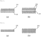
- a conventional optical sheet having a micropattern or a nanopattern is manufactured by coating the upper surface of a substrate film (a substrate layer) made of PET, PC, PMMA, TAC, COC, or COP with a curable resin and then performing patterning (forming a pattern layer).
- a substrate film made of PET, PC, PMMA, TAC, COC, or COP
- patterning forming a pattern layer.
- FIG. 1 light loss may occur at the interface between the substrate layer 100 and the pattern layer 200, thereby remarkably decreasing transmittance or frequently causing light reflection.
- a conventional pattern transfer process such as a roll-to-roll process may be directly applied even without the use of an additional process, thus forming an non-substrate(substrate-less)-type optical sheet having no substrate layer, as shown in FIG. 2 , in which a nano-scale pattern having a pitch of 50 to 500 nm and an aspect ratio of 1.0 to 5.0 is formed on at least one surface thereof.
- the curable resin composition of the present invention preferably includes 100 parts by weight of a urethane acrylate having a weight average molecular weight of 100 to 30,000 and 75 to 250 parts by weight of a fluorine-containing siloxane-acrylate oligomer having a weight average molecular weight of 100 to 10,000 based on 100 parts by weight of the urethane acrylate.
- individual weight average molecular weights preferably fall in the above ranges, and the weight average molecular weights may be determined using a method of measuring the molecular weight of a polymer such as MALDS (Matrix-Assisted Laser Desorption Ionization Mass Spectrometry) or GPC (Gel Permeation Chromatography).
- MALDS Microx-Assisted Laser Desorption Ionization Mass Spectrometry
- GPC Gel Permeation Chromatography
- the urethane acrylate of the present invention is a main component that is added to impart the durability of an optical sheet, resistance to curling and yellowing, flexibility, and supporting capability as a single layer, and may be used in an amount of 20 to 40 wt% based on the total weight of the curable resin in terms of ensuring the above properties.
- the fluorine-containing siloxane-acrylate oligomer is a main component that participates in a curing reaction, and has a molecular structure in which siloxane-acrylate is substituted with fluorine and thus may play an important role in increasing releasability from the mold after the curing process.
- silicone acrylate having a weight average molecular weight of 900 to 1,500 is used to attain releasability from the mold. Silicone acrylate enables the transfer of a pattern on a micro scale but does not satisfy releasability on a nano scale.
- a fluorine resin may be used to obtain releasability. In this case, the resin tends to remain in the mold and contaminates the mold, making it difficult to attain repeatability.
- an oligomer configured such that siloxane-acrylate is substituted with fluorine is used as a main component, thus attaining both releasability and pattern repeatability.
- the amount of the fluorine-containing siloxane-acrylate oligomer is less than 75 parts by weight based on 100 parts by weight of the urethane acrylate, releasability and a transfer rate may decrease, thus causing pattern clustering.
- the amount thereof is 250 parts by weight or less, releasability may be sufficiently ensured.
- the amount thereof preferably does not exceed 250 parts by weight, taking into consideration the price of fluorine.
- the curable resin composition may further include, based on 100 parts by weight of the urethane acrylate, 60 to 125 parts by weight of a diluent and 10 to 25 parts by weight of a polymerization initiator.
- the diluent may be added to adjust the viscosity of the resin, and is preferably an acrylate-based monomer. Since all of the diluent and the main components contain acrylate-based monomers, the double bond of the vinyl group breaks down and thus radical polymerization occurs and a curing reaction may be easily carried out.
- the amount of the diluent preferably falls in the above range in order to maintain the viscosity of the resin in the range of 100 to 300 cps. If the viscosity of the curable resin composition is less than 100 cps, flowability of the composition may excessively increase during the roll-to-roll imprinting process, thus causing variation in film thickness. On the other hand, if the viscosity thereof exceeds 300 cps, the composition may penetrate into the nanopattern, making it difficult to form a desired pattern.
- the polymerization initiator may be at least one selected from the group consisting of a phosphine oxide-based polymerization initiator, a propanone-based polymerization initiator, a ketone-based polymerization initiator and a formate-based polymerization initiator, and is preferably added in an amount of 10 to 25 parts by weight based on 100 parts by weight of the urethane acrylate in order to prevent coloring or deterioration of mechanical strength during the polymerization reaction.
- the curable resin composition of the present invention may further include, but is not necessarily limited to, at least one additive selected from the group consisting of a UV absorbent, a UV stabilizer, a color stabilizer, a leveling agent, an antioxidant, a defoaming agent, and an antistatic agent.
- at least one additive selected from the group consisting of a UV absorbent, a UV stabilizer, a color stabilizer, a leveling agent, an antioxidant, a defoaming agent, and an antistatic agent.
- the optical sheet of the present invention may be manufactured using a roll-to-roll process or a stamp process, and preferably a roll-to-roll process.
- the roll-to-roll process is performed using, as shown in FIGS. 3 to 5 , two guide rolls 11 acting as shafts, a release mold 1, 2 having a nanopattern to form a pattern on an optical sheet, and a slot die 14 for feeding the curable resin composition in the form of a sheet.
- the curable resin composition is fed into a slot die to form a single layer.
- the thickness thereof may be set in the range of 10 to 500 ⁇ m by adjusting the line speed of the roll-to-roll system depending on the end use thereof, but is not necessarily limited thereto.
- the single layer discharged from the slot die may be primarily cured before the formation of the nanopattern, but the present invention is not necessarily limited thereto.
- the pattern of the mold is transferred on one surface or both surfaces of the single layer, thus forming the pattern (S2).
- the pattern may have a micro lens shape in which a hemispherical shape, a cylindrical shape, a trigonal pyramid shape, or a quadrangular pyramid shape is repeated, or a line grid shape, such as a prism or a lenticular pattern, but the present invention is not limited thereto.
- the nanopattern unit shape which is observed on the cross-section when the single layer having the pattern is cut in a vertical direction, preferably has a pitch of 50 to 500 nm and an aspect ratio of 1.0 to 5.0.
- the pattern has a nano size within the above range, thus alleviating changes in refractive index due to the fine irregular structure.
- the formation of the pattern on the single layer in (S2) is preferably carried out in a manner in which the single layer is pre-cured with light at a dose of 50 to 150 mj/cm 2 along with the pattern transfer.
- pre-curing is implemented by irradiating the resin composition with light at a dose of 50 to 150 mj/cm 2 , pattern crushing or layer tearing may be prevented upon release of the pattern from the mold, and curling properties and transmittance of the final optical sheet may be ensured, even without the use of the substrate layer.
- the release mold has to be efficiently released after the transfer of the pattern onto the single layer so as to be repeatedly usable in the roll-to-roll process, and should also be easily washed.
- the release mold may be coated with at least one release agent selected from the group consisting of silicone, fluorine and Teflon.
- the surface of the mold is treated with the release agent in a manner in which the mold body is immersed in the diluted solution of the release agent, or in which the release agent or the diluted solution thereof is applied on the surface of the mold body having the fine irregular structure.
- the immersion of the mold body in the diluted solution of the release agent is more preferably conducted because the surface of the mold body having the fine irregular structure may be uniformly treated with the release agent.
- the single layer having the nanopattern formed in (S2) may be irradiated with light at a dose of 150 mj/cm 2 or more, and preferably 150 to 1,000 mj/cm 2 , thus finally manufacturing an non-substrate(substrate-less)-type optical sheet having a nanopattern (S3).
- the light dose is less than 150 mj/cm 2 , curing is not performed, and reliability may become problematic.
- the light dose exceeds 1,000 mj/cm 2 , brittleness may occur due to over-curing, undesirably causing problems related to handling or reliability.
- the light dose is not necessarily limited thereto, and the light dose and the degree of curing may become optimal taking into account the line speed in the roll-to-roll system upon curing.
- the optical sheet of the present invention may exhibit a transmittance of 95% or more upon irradiation with light at 550 nm and a curl value of 0 mm to 2.0 mm at 23°C.
- the optical sheet has the above optical characteristics and properties, and the present invention is able to provide an non-substrate(substrate-less)-type optical sheet having improved transmittance and stable reliability, compared to optical sheets including a substrate layer.
- a curable resin composition having a viscosity of 150 cps was prepared by mixing, based on the total weight of a mixture, 50 wt% of, as a main compound, a fluorine-containing siloxane-acrylate oligomer having a weight average molecular weight of 5,500, 20 wt% of polyurethane acrylate having a weight average molecular weight of 1,800, 25 wt% of 1,6-hexandiol diacrylate as a diluent and 5 wt% of 1-hydroxy-cyclohexylphenyl-ketone as a polymerization initiator, and was then fed into a roll-to-roll system in which a release mold (available from Soken, Japan) was provided on only one surface of a sheet, as shown in FIG. 3 or 4 , thus manufacturing an non-substrate(substrate-less)-type optical sheet having a nanopattern through the following method.
- An optical sheet having a nanopattern was manufactured in the same manner as in Example 1, with the exception that the same pattern as in Example 1 was formed on both surfaces of the single layer in (S2) (the upper and lower patterns are the same) as shown in FIG. 5 .
- An optical sheet having a nanopattern was manufactured in the same manner as in Example 1, with the exception that the light dose was changed to 50 mj/cm 2 upon pre-curing in (S2).
- An optical sheet having a nanopattern was manufactured in the same manner as in Example 1, with the exception that the light dose was changed to 150 mj/cm 2 upon pre-curing in (S2).
- An optical sheet having a nanopattern was manufactured in the same manner as in Example 1, with the exception that 30 wt% of the fluorine-containing siloxane-acrylate oligomer and 40 wt% of the urethane acrylate were added.
- An optical sheet having a nanopattern with a substrate layer was manufactured in the same manner as in Example 1, with the exception that the same curable composition as in Example 1 was used but a PET film (KOLON, 50 ⁇ m) was used as a substrate layer, and the curable composition was applied to a thickness of 25 ⁇ m on the substrate layer in (S1).
- a PET film KOLON, 50 ⁇ m
- Example 2 The same curable composition as in Example 1 was used, and an attempt was made to omit pre-curing in (S2), but the curable composition became stuck to the mold, making it impossible to manufacture a sheet.
- An optical sheet having a nanopattern was manufactured in the same manner as in Example 1, with the exception that the same curable composition as in Example 1 was used and the light dose was changed to 45 mj/cm 2 upon pre-curing in (S2).
- An optical sheet having a nanopattern was manufactured in the same manner as in Example 1, with the exception that the same curable composition as in Example 1 was used and the light dose was changed to 160 mj/cm 2 upon pre-curing in (S2).
- An non-substrate(substrate-less)-type optical sheet having a nanopattern was manufactured in the same manner as in Example 1, with the exception that 10 wt% of the fluorine-containing siloxane-acrylate oligomer and 60 wt% of the urethane acrylate were added.
- An non-substrate(substrate-less)-type optical sheet having a nanopattern was manufactured in the same manner as in Example 3, with the exception that 30 wt% of polysiloxane acrylate (available from Miwon) having a molecular weight of 1,100 was added in lieu of the fluorine-containing siloxane-acrylate oligomer.
- polysiloxane acrylate available from Miwon
- Comparative Example 7 Formation of non-substrate(substrate-less)-type optical sheet using curable composition having different component and different component ratio
- An non-substrate(substrate-less)-type optical sheet having a nanopattern was manufactured in the same manner as in Example 3, with the exception that 10 wt% of polysiloxane acrylate (available from Miwon) was further added and 30 wt% of the urethane acrylate was added.
- Example 8 Compound A 1) 50 30 10 - 30 - Compound B 2) - - - 30 10 - Compound C 3) 20 40 60 40 30 70 Diluent 4) 25 25 25 25 25 25 25 25 Curing agent 5) 5 5 5 5 5 1)
- the sheet was cut to a size of 5cm*5cm, and the transmittance thereof was measured at a wavelength of 550 nm using a spectrophotometer (CM-3600).
- a sample was subjected to reliability testing under the condition that it was allowed to stand at a temperature of 65°C and a humidity of 85% for 1,000 hr, after which the sample was allowed to stand at room temperature (23°C) for 1 hr, and the curling properties thereof were measured using a steel ruler or a gap gauge.
- the amount of the fluorine-containing siloxane-acrylate oligomer was less than 30 wt% based on the total weight of the composition, as in Comparative Example 5, pattern clustering occurred, thus making it impossible to form a fine nanopattern, thereby significantly decreasing light transmittance.
- Comparative Example 6 using the typical polysiloxane acrylate containing no fluorine in lieu of the fluorine-containing siloxane-acrylate oligomer, releasability was significantly decreased, and thus the nanopattern was not formed.
Landscapes
- Physics & Mathematics (AREA)
- General Physics & Mathematics (AREA)
- Optics & Photonics (AREA)
- Engineering & Computer Science (AREA)
- Mechanical Engineering (AREA)
- Nonlinear Science (AREA)
- Chemical & Material Sciences (AREA)
- Crystallography & Structural Chemistry (AREA)
- Mathematical Physics (AREA)
- Optical Elements Other Than Lenses (AREA)
- Moulds For Moulding Plastics Or The Like (AREA)
- Macromonomer-Based Addition Polymer (AREA)
- Laminated Bodies (AREA)
- Liquid Crystal (AREA)
- Surface Treatment Of Optical Elements (AREA)
- Shaping Of Tube Ends By Bending Or Straightening (AREA)
Applications Claiming Priority (3)
| Application Number | Priority Date | Filing Date | Title |
|---|---|---|---|
| KR20140128162 | 2014-09-25 | ||
| KR1020150134921A KR101776065B1 (ko) | 2014-09-25 | 2015-09-23 | 나노패턴을 포함하는 광학시트 및 그 제조방법 |
| PCT/KR2015/010207 WO2016048091A1 (ko) | 2014-09-25 | 2015-09-25 | 나노패턴을 포함하는 광학시트 및 그 제조방법 |
Publications (3)
| Publication Number | Publication Date |
|---|---|
| EP3199983A1 true EP3199983A1 (de) | 2017-08-02 |
| EP3199983A4 EP3199983A4 (de) | 2018-05-02 |
| EP3199983B1 EP3199983B1 (de) | 2020-01-01 |
Family
ID=55799792
Family Applications (1)
| Application Number | Title | Priority Date | Filing Date |
|---|---|---|---|
| EP15844402.6A Active EP3199983B1 (de) | 2014-09-25 | 2015-09-25 | Optische folie mit nanostruktur und verfahren zur herstellung derselben |
Country Status (5)
| Country | Link |
|---|---|
| US (1) | US10132962B2 (de) |
| EP (1) | EP3199983B1 (de) |
| JP (1) | JP6442602B2 (de) |
| KR (1) | KR101776065B1 (de) |
| CN (1) | CN106716183B (de) |
Families Citing this family (3)
| Publication number | Priority date | Publication date | Assignee | Title |
|---|---|---|---|---|
| KR20170079671A (ko) * | 2015-12-30 | 2017-07-10 | 코오롱인더스트리 주식회사 | 와이어 그리드 편광판 및 이를 포함한 액정표시장치 |
| KR102921585B1 (ko) * | 2020-08-27 | 2026-01-30 | 주식회사 엘지화학 | 고흡수성 수지 필름의 제조방법 |
| KR102547363B1 (ko) * | 2023-02-07 | 2023-06-22 | 문제희 | 무기재 이중패턴필름 및 그 제조방법 |
Family Cites Families (19)
| Publication number | Priority date | Publication date | Assignee | Title |
|---|---|---|---|---|
| US20070204953A1 (en) * | 2006-02-21 | 2007-09-06 | Ching-Bin Lin | Method for forming structured film as molded by tape die |
| US7854864B2 (en) | 2006-04-28 | 2010-12-21 | Konica Minolta Opto, Inc. | Method for manufacturing an optical film having a convexoconcave structure |
| KR20080014429A (ko) | 2006-08-11 | 2008-02-14 | 삼성전자주식회사 | 임프린트 방법 |
| WO2009041646A1 (ja) * | 2007-09-28 | 2009-04-02 | Asahi Glass Company, Limited | 光硬化性組成物、微細パターン形成体の製造方法および光学素子 |
| KR20090084340A (ko) | 2008-02-01 | 2009-08-05 | 주식회사 동진쎄미켐 | 광경화형 수지 조성물 및 이를 이용한 수지 몰드의제조방법 |
| JP5306903B2 (ja) * | 2008-07-02 | 2013-10-02 | 富士フイルム株式会社 | インプリント用硬化性組成物、これを用いた硬化物およびその製造方法、並びに、液晶表示装置用部材 |
| JP5175672B2 (ja) * | 2008-09-26 | 2013-04-03 | 富士フイルム株式会社 | 防眩フィルム、反射防止フィルム、偏光板及び画像表示装置 |
| JP2010186979A (ja) * | 2008-12-03 | 2010-08-26 | Fujifilm Corp | インプリント用硬化性組成物、パターン形成方法およびパターン |
| WO2010143503A1 (ja) * | 2009-06-12 | 2010-12-16 | シャープ株式会社 | 反射防止膜、表示装置及び透光部材 |
| KR101653626B1 (ko) | 2009-07-13 | 2016-09-02 | 주식회사 동진쎄미켐 | 광경화형 함불소 수지 조성물 및 이를 이용한 수지 몰드의 제조방법 |
| JP2012204584A (ja) | 2011-03-25 | 2012-10-22 | Fujifilm Corp | ナノインプリント方法 |
| SG2014011746A (en) * | 2011-08-17 | 2014-08-28 | 3M Innovative Properties Co | Nanostructured articles and methods to make the same |
| KR101226229B1 (ko) * | 2011-08-26 | 2013-01-28 | 주식회사 엘지화학 | 반사 방지 필름 |
| JP5976523B2 (ja) * | 2011-12-28 | 2016-08-23 | 富士フイルム株式会社 | 光学部材セット及びこれを用いた固体撮像素子 |
| TWI489522B (zh) * | 2012-03-12 | 2015-06-21 | 旭化成電子材料股份有限公司 | Mold, resist layer and its manufacturing method and concave and convex structure |
| US20150111032A1 (en) * | 2012-03-23 | 2015-04-23 | Lintec Corporation | Film, Sheet Substrate for Processing Workpiece, and Sheet for Processing Workpiece |
| JP2013254130A (ja) * | 2012-06-08 | 2013-12-19 | Dexerials Corp | 光学素子およびその製造方法、表示素子、ならびに投射型画像表示装置 |
| US20150079341A1 (en) * | 2013-09-16 | 2015-03-19 | Tokyo University of Sci. Ed. Foundation Admin. Org | Fabrication method of resin compact, resin compact, and mold |
| JP6186294B2 (ja) * | 2014-03-07 | 2017-08-23 | 富士フイルム株式会社 | 反射防止フィルム、偏光板、画像表示装置、及び反射防止フィルムの製造方法 |
-
2015
- 2015-09-23 KR KR1020150134921A patent/KR101776065B1/ko not_active Expired - Fee Related
- 2015-09-25 CN CN201580051845.6A patent/CN106716183B/zh not_active Expired - Fee Related
- 2015-09-25 JP JP2017516141A patent/JP6442602B2/ja active Active
- 2015-09-25 US US15/513,345 patent/US10132962B2/en not_active Expired - Fee Related
- 2015-09-25 EP EP15844402.6A patent/EP3199983B1/de active Active
Also Published As
| Publication number | Publication date |
|---|---|
| CN106716183B (zh) | 2018-11-02 |
| JP6442602B2 (ja) | 2018-12-19 |
| JP2017531207A (ja) | 2017-10-19 |
| KR101776065B1 (ko) | 2017-09-07 |
| EP3199983A4 (de) | 2018-05-02 |
| CN106716183A (zh) | 2017-05-24 |
| US20170299776A1 (en) | 2017-10-19 |
| EP3199983B1 (de) | 2020-01-01 |
| KR20160036508A (ko) | 2016-04-04 |
| US10132962B2 (en) | 2018-11-20 |
Similar Documents
| Publication | Publication Date | Title |
|---|---|---|
| US11339288B2 (en) | Photocurable composition and coating layer including cured product thereof | |
| AT516559B1 (de) | Poly- bzw. Präpolymerzusammensetzung bzw. Prägelack, umfassend eine derartige Zusammensetzung sowie Verwendung derselben | |
| TW201801928A (zh) | 雙軸配向聚丙烯膜 | |
| CN105556347A (zh) | 结构体及其制造方法,以及具有该结构体的物品 | |
| JP7006710B2 (ja) | セラミックグリーンシート製造用離型フィルム | |
| EP3615598B1 (de) | Transparente kompositfolie mit hartem überzug, arbeitsweise zur bildung einer solchen folie und biegsame anzeigevorrichtung enthaltend eine solche folie | |
| EP2803706A1 (de) | Hartbeschichtungszusammensetzung und schmuckfilm mit verminderter vergilbung damit | |
| EP3199983B1 (de) | Optische folie mit nanostruktur und verfahren zur herstellung derselben | |
| JP2020090090A (ja) | 超低い離型力を有する離型フィルム及びその製造方法 | |
| KR102382953B1 (ko) | 복층 필름 및 그의 제조 방법 | |
| JP2019028109A (ja) | 複層フィルム及びその製造方法 | |
| CN112457694A (zh) | 一种环保型紫外光固化非硅离型剂,离型膜及其制备方法 | |
| JP2017210579A (ja) | ウレタンアクリレートを用いた光硬化性樹脂成形体 | |
| JP2009167315A (ja) | 多孔質体の製造方法 | |
| US10967563B2 (en) | Method for reducing drawing force in forming process of photocurable material | |
| JP6442973B2 (ja) | 微細構造形成用光硬化型組成物及びその硬化物 | |
| JP5781464B2 (ja) | 塗膜付きフィルムの製造方法 | |
| KR101218148B1 (ko) | 굴절율 조절이 용이한 광학용 폴리에스테르 필름 | |
| TWI868120B (zh) | 光硬化性組成物、凹凸結構體的製造方法、形成微細凹凸圖案的方法及凹凸結構體 | |
| KR102115519B1 (ko) | 광학필름 | |
| JP2019055567A (ja) | 離型フィルム | |
| Almanza-Workman et al. | Fabrication of three-dimensional imprint lithography templates by colloidal dispersions | |
| TWI647271B (zh) | 活性能量線硬化性組成物、硬化物、光學零件及活性能量線硬化性組成物之製造方法 | |
| JP7262324B2 (ja) | 成形体、成形体の製造方法、組成物、及び組成物の製造方法 | |
| CN105492475A (zh) | 保护薄膜用聚丙烯树脂以及保护薄膜 |
Legal Events
| Date | Code | Title | Description |
|---|---|---|---|
| STAA | Information on the status of an ep patent application or granted ep patent |
Free format text: STATUS: THE INTERNATIONAL PUBLICATION HAS BEEN MADE |
|
| PUAI | Public reference made under article 153(3) epc to a published international application that has entered the european phase |
Free format text: ORIGINAL CODE: 0009012 |
|
| STAA | Information on the status of an ep patent application or granted ep patent |
Free format text: STATUS: REQUEST FOR EXAMINATION WAS MADE |
|
| 17P | Request for examination filed |
Effective date: 20170316 |
|
| AK | Designated contracting states |
Kind code of ref document: A1 Designated state(s): AL AT BE BG CH CY CZ DE DK EE ES FI FR GB GR HR HU IE IS IT LI LT LU LV MC MK MT NL NO PL PT RO RS SE SI SK SM TR |
|
| AX | Request for extension of the european patent |
Extension state: BA ME |
|
| DAV | Request for validation of the european patent (deleted) | ||
| DAX | Request for extension of the european patent (deleted) | ||
| REG | Reference to a national code |
Ref country code: DE Ref legal event code: R079 Ref document number: 602015044876 Country of ref document: DE Free format text: PREVIOUS MAIN CLASS: G02B0001110000 Ipc: G02B0001118000 |
|
| A4 | Supplementary search report drawn up and despatched |
Effective date: 20180404 |
|
| RIC1 | Information provided on ipc code assigned before grant |
Ipc: G02F 1/1335 20060101ALI20180327BHEP Ipc: C08J 5/18 20060101ALI20180327BHEP Ipc: G02B 1/118 20150101AFI20180327BHEP |
|
| RAP1 | Party data changed (applicant data changed or rights of an application transferred) |
Owner name: KOLON INDUSTRIES, INC. |
|
| GRAP | Despatch of communication of intention to grant a patent |
Free format text: ORIGINAL CODE: EPIDOSNIGR1 |
|
| STAA | Information on the status of an ep patent application or granted ep patent |
Free format text: STATUS: GRANT OF PATENT IS INTENDED |
|
| INTG | Intention to grant announced |
Effective date: 20190813 |
|
| GRAS | Grant fee paid |
Free format text: ORIGINAL CODE: EPIDOSNIGR3 |
|
| GRAA | (expected) grant |
Free format text: ORIGINAL CODE: 0009210 |
|
| STAA | Information on the status of an ep patent application or granted ep patent |
Free format text: STATUS: THE PATENT HAS BEEN GRANTED |
|
| AK | Designated contracting states |
Kind code of ref document: B1 Designated state(s): AL AT BE BG CH CY CZ DE DK EE ES FI FR GB GR HR HU IE IS IT LI LT LU LV MC MK MT NL NO PL PT RO RS SE SI SK SM TR |
|
| REG | Reference to a national code |
Ref country code: GB Ref legal event code: FG4D |
|
| REG | Reference to a national code |
Ref country code: CH Ref legal event code: EP Ref country code: AT Ref legal event code: REF Ref document number: 1220484 Country of ref document: AT Kind code of ref document: T Effective date: 20200115 |
|
| REG | Reference to a national code |
Ref country code: IE Ref legal event code: FG4D |
|
| REG | Reference to a national code |
Ref country code: DE Ref legal event code: R096 Ref document number: 602015044876 Country of ref document: DE |
|
| REG | Reference to a national code |
Ref country code: NL Ref legal event code: MP Effective date: 20200101 |
|
| REG | Reference to a national code |
Ref country code: LT Ref legal event code: MG4D |
|
| PG25 | Lapsed in a contracting state [announced via postgrant information from national office to epo] |
Ref country code: FI Free format text: LAPSE BECAUSE OF FAILURE TO SUBMIT A TRANSLATION OF THE DESCRIPTION OR TO PAY THE FEE WITHIN THE PRESCRIBED TIME-LIMIT Effective date: 20200101 Ref country code: RS Free format text: LAPSE BECAUSE OF FAILURE TO SUBMIT A TRANSLATION OF THE DESCRIPTION OR TO PAY THE FEE WITHIN THE PRESCRIBED TIME-LIMIT Effective date: 20200101 Ref country code: NO Free format text: LAPSE BECAUSE OF FAILURE TO SUBMIT A TRANSLATION OF THE DESCRIPTION OR TO PAY THE FEE WITHIN THE PRESCRIBED TIME-LIMIT Effective date: 20200401 Ref country code: PT Free format text: LAPSE BECAUSE OF FAILURE TO SUBMIT A TRANSLATION OF THE DESCRIPTION OR TO PAY THE FEE WITHIN THE PRESCRIBED TIME-LIMIT Effective date: 20200527 Ref country code: CZ Free format text: LAPSE BECAUSE OF FAILURE TO SUBMIT A TRANSLATION OF THE DESCRIPTION OR TO PAY THE FEE WITHIN THE PRESCRIBED TIME-LIMIT Effective date: 20200101 Ref country code: NL Free format text: LAPSE BECAUSE OF FAILURE TO SUBMIT A TRANSLATION OF THE DESCRIPTION OR TO PAY THE FEE WITHIN THE PRESCRIBED TIME-LIMIT Effective date: 20200101 Ref country code: LT Free format text: LAPSE BECAUSE OF FAILURE TO SUBMIT A TRANSLATION OF THE DESCRIPTION OR TO PAY THE FEE WITHIN THE PRESCRIBED TIME-LIMIT Effective date: 20200101 |
|
| PG25 | Lapsed in a contracting state [announced via postgrant information from national office to epo] |
Ref country code: IS Free format text: LAPSE BECAUSE OF FAILURE TO SUBMIT A TRANSLATION OF THE DESCRIPTION OR TO PAY THE FEE WITHIN THE PRESCRIBED TIME-LIMIT Effective date: 20200501 Ref country code: BG Free format text: LAPSE BECAUSE OF FAILURE TO SUBMIT A TRANSLATION OF THE DESCRIPTION OR TO PAY THE FEE WITHIN THE PRESCRIBED TIME-LIMIT Effective date: 20200401 Ref country code: HR Free format text: LAPSE BECAUSE OF FAILURE TO SUBMIT A TRANSLATION OF THE DESCRIPTION OR TO PAY THE FEE WITHIN THE PRESCRIBED TIME-LIMIT Effective date: 20200101 Ref country code: SE Free format text: LAPSE BECAUSE OF FAILURE TO SUBMIT A TRANSLATION OF THE DESCRIPTION OR TO PAY THE FEE WITHIN THE PRESCRIBED TIME-LIMIT Effective date: 20200101 Ref country code: LV Free format text: LAPSE BECAUSE OF FAILURE TO SUBMIT A TRANSLATION OF THE DESCRIPTION OR TO PAY THE FEE WITHIN THE PRESCRIBED TIME-LIMIT Effective date: 20200101 Ref country code: GR Free format text: LAPSE BECAUSE OF FAILURE TO SUBMIT A TRANSLATION OF THE DESCRIPTION OR TO PAY THE FEE WITHIN THE PRESCRIBED TIME-LIMIT Effective date: 20200402 |
|
| REG | Reference to a national code |
Ref country code: DE Ref legal event code: R097 Ref document number: 602015044876 Country of ref document: DE |
|
| PG25 | Lapsed in a contracting state [announced via postgrant information from national office to epo] |
Ref country code: EE Free format text: LAPSE BECAUSE OF FAILURE TO SUBMIT A TRANSLATION OF THE DESCRIPTION OR TO PAY THE FEE WITHIN THE PRESCRIBED TIME-LIMIT Effective date: 20200101 Ref country code: DK Free format text: LAPSE BECAUSE OF FAILURE TO SUBMIT A TRANSLATION OF THE DESCRIPTION OR TO PAY THE FEE WITHIN THE PRESCRIBED TIME-LIMIT Effective date: 20200101 Ref country code: SK Free format text: LAPSE BECAUSE OF FAILURE TO SUBMIT A TRANSLATION OF THE DESCRIPTION OR TO PAY THE FEE WITHIN THE PRESCRIBED TIME-LIMIT Effective date: 20200101 Ref country code: ES Free format text: LAPSE BECAUSE OF FAILURE TO SUBMIT A TRANSLATION OF THE DESCRIPTION OR TO PAY THE FEE WITHIN THE PRESCRIBED TIME-LIMIT Effective date: 20200101 Ref country code: SM Free format text: LAPSE BECAUSE OF FAILURE TO SUBMIT A TRANSLATION OF THE DESCRIPTION OR TO PAY THE FEE WITHIN THE PRESCRIBED TIME-LIMIT Effective date: 20200101 Ref country code: RO Free format text: LAPSE BECAUSE OF FAILURE TO SUBMIT A TRANSLATION OF THE DESCRIPTION OR TO PAY THE FEE WITHIN THE PRESCRIBED TIME-LIMIT Effective date: 20200101 |
|
| PLBE | No opposition filed within time limit |
Free format text: ORIGINAL CODE: 0009261 |
|
| STAA | Information on the status of an ep patent application or granted ep patent |
Free format text: STATUS: NO OPPOSITION FILED WITHIN TIME LIMIT |
|
| REG | Reference to a national code |
Ref country code: AT Ref legal event code: MK05 Ref document number: 1220484 Country of ref document: AT Kind code of ref document: T Effective date: 20200101 |
|
| 26N | No opposition filed |
Effective date: 20201002 |
|
| PG25 | Lapsed in a contracting state [announced via postgrant information from national office to epo] |
Ref country code: IT Free format text: LAPSE BECAUSE OF FAILURE TO SUBMIT A TRANSLATION OF THE DESCRIPTION OR TO PAY THE FEE WITHIN THE PRESCRIBED TIME-LIMIT Effective date: 20200101 Ref country code: AT Free format text: LAPSE BECAUSE OF FAILURE TO SUBMIT A TRANSLATION OF THE DESCRIPTION OR TO PAY THE FEE WITHIN THE PRESCRIBED TIME-LIMIT Effective date: 20200101 |
|
| PG25 | Lapsed in a contracting state [announced via postgrant information from national office to epo] |
Ref country code: SI Free format text: LAPSE BECAUSE OF FAILURE TO SUBMIT A TRANSLATION OF THE DESCRIPTION OR TO PAY THE FEE WITHIN THE PRESCRIBED TIME-LIMIT Effective date: 20200101 Ref country code: PL Free format text: LAPSE BECAUSE OF FAILURE TO SUBMIT A TRANSLATION OF THE DESCRIPTION OR TO PAY THE FEE WITHIN THE PRESCRIBED TIME-LIMIT Effective date: 20200101 |
|
| REG | Reference to a national code |
Ref country code: DE Ref legal event code: R119 Ref document number: 602015044876 Country of ref document: DE |
|
| PG25 | Lapsed in a contracting state [announced via postgrant information from national office to epo] |
Ref country code: MC Free format text: LAPSE BECAUSE OF FAILURE TO SUBMIT A TRANSLATION OF THE DESCRIPTION OR TO PAY THE FEE WITHIN THE PRESCRIBED TIME-LIMIT Effective date: 20200101 |
|
| REG | Reference to a national code |
Ref country code: CH Ref legal event code: PL |
|
| GBPC | Gb: european patent ceased through non-payment of renewal fee |
Effective date: 20200925 |
|
| REG | Reference to a national code |
Ref country code: BE Ref legal event code: MM Effective date: 20200930 |
|
| PG25 | Lapsed in a contracting state [announced via postgrant information from national office to epo] |
Ref country code: LU Free format text: LAPSE BECAUSE OF NON-PAYMENT OF DUE FEES Effective date: 20200925 |
|
| PG25 | Lapsed in a contracting state [announced via postgrant information from national office to epo] |
Ref country code: FR Free format text: LAPSE BECAUSE OF NON-PAYMENT OF DUE FEES Effective date: 20200930 Ref country code: DE Free format text: LAPSE BECAUSE OF NON-PAYMENT OF DUE FEES Effective date: 20210401 |
|
| PG25 | Lapsed in a contracting state [announced via postgrant information from national office to epo] |
Ref country code: GB Free format text: LAPSE BECAUSE OF NON-PAYMENT OF DUE FEES Effective date: 20200925 Ref country code: LI Free format text: LAPSE BECAUSE OF NON-PAYMENT OF DUE FEES Effective date: 20200930 Ref country code: IE Free format text: LAPSE BECAUSE OF NON-PAYMENT OF DUE FEES Effective date: 20200925 Ref country code: CH Free format text: LAPSE BECAUSE OF NON-PAYMENT OF DUE FEES Effective date: 20200930 Ref country code: BE Free format text: LAPSE BECAUSE OF NON-PAYMENT OF DUE FEES Effective date: 20200930 |
|
| PG25 | Lapsed in a contracting state [announced via postgrant information from national office to epo] |
Ref country code: TR Free format text: LAPSE BECAUSE OF FAILURE TO SUBMIT A TRANSLATION OF THE DESCRIPTION OR TO PAY THE FEE WITHIN THE PRESCRIBED TIME-LIMIT Effective date: 20200101 Ref country code: MT Free format text: LAPSE BECAUSE OF FAILURE TO SUBMIT A TRANSLATION OF THE DESCRIPTION OR TO PAY THE FEE WITHIN THE PRESCRIBED TIME-LIMIT Effective date: 20200101 Ref country code: CY Free format text: LAPSE BECAUSE OF FAILURE TO SUBMIT A TRANSLATION OF THE DESCRIPTION OR TO PAY THE FEE WITHIN THE PRESCRIBED TIME-LIMIT Effective date: 20200101 |
|
| PG25 | Lapsed in a contracting state [announced via postgrant information from national office to epo] |
Ref country code: MK Free format text: LAPSE BECAUSE OF FAILURE TO SUBMIT A TRANSLATION OF THE DESCRIPTION OR TO PAY THE FEE WITHIN THE PRESCRIBED TIME-LIMIT Effective date: 20200101 Ref country code: AL Free format text: LAPSE BECAUSE OF FAILURE TO SUBMIT A TRANSLATION OF THE DESCRIPTION OR TO PAY THE FEE WITHIN THE PRESCRIBED TIME-LIMIT Effective date: 20200101 |