EP3200232B1 - Organisches leuchtdioden-arraysubstrat und herstellungsverfahren dafür - Google Patents
Organisches leuchtdioden-arraysubstrat und herstellungsverfahren dafür Download PDFInfo
- Publication number
- EP3200232B1 EP3200232B1 EP15729325.9A EP15729325A EP3200232B1 EP 3200232 B1 EP3200232 B1 EP 3200232B1 EP 15729325 A EP15729325 A EP 15729325A EP 3200232 B1 EP3200232 B1 EP 3200232B1
- Authority
- EP
- European Patent Office
- Prior art keywords
- conductive unit
- cathode
- layer
- array substrate
- oled
- Prior art date
- Legal status (The legal status is an assumption and is not a legal conclusion. Google has not performed a legal analysis and makes no representation as to the accuracy of the status listed.)
- Active
Links
Images


Classifications
-
- H—ELECTRICITY
- H10—SEMICONDUCTOR DEVICES; ELECTRIC SOLID-STATE DEVICES NOT OTHERWISE PROVIDED FOR
- H10K—ORGANIC ELECTRIC SOLID-STATE DEVICES
- H10K59/00—Integrated devices, or assemblies of multiple devices, comprising at least one organic light-emitting element covered by group H10K50/00
- H10K59/10—OLED displays
- H10K59/12—Active-matrix OLED [AMOLED] displays
- H10K59/122—Pixel-defining structures or layers, e.g. banks
-
- H—ELECTRICITY
- H10—SEMICONDUCTOR DEVICES; ELECTRIC SOLID-STATE DEVICES NOT OTHERWISE PROVIDED FOR
- H10K—ORGANIC ELECTRIC SOLID-STATE DEVICES
- H10K59/00—Integrated devices, or assemblies of multiple devices, comprising at least one organic light-emitting element covered by group H10K50/00
- H10K59/10—OLED displays
- H10K59/12—Active-matrix OLED [AMOLED] displays
- H10K59/131—Interconnections, e.g. wiring lines or terminals
- H10K59/1315—Interconnections, e.g. wiring lines or terminals comprising structures specially adapted for lowering the resistance
-
- H—ELECTRICITY
- H10—SEMICONDUCTOR DEVICES; ELECTRIC SOLID-STATE DEVICES NOT OTHERWISE PROVIDED FOR
- H10K—ORGANIC ELECTRIC SOLID-STATE DEVICES
- H10K2102/00—Constructional details relating to the organic devices covered by this subclass
-
- H—ELECTRICITY
- H10—SEMICONDUCTOR DEVICES; ELECTRIC SOLID-STATE DEVICES NOT OTHERWISE PROVIDED FOR
- H10K—ORGANIC ELECTRIC SOLID-STATE DEVICES
- H10K59/00—Integrated devices, or assemblies of multiple devices, comprising at least one organic light-emitting element covered by group H10K50/00
- H10K59/10—OLED displays
- H10K59/12—Active-matrix OLED [AMOLED] displays
- H10K59/1201—Manufacture or treatment
Definitions
- the present disclosure relates to the field of organic light emitting diode (OLED) display, in particular to an organic light emitting diode array substrate and its manufacturing method, as well as a display device.
- OLED organic light emitting diode
- a transparent display may allow a viewer to observe a background behind a display screen.
- Such a novel display effect broadens the application field of display, which may be applied to display devices such as a mobile phone, a laptop PC, a display window, a refrigerator door, an on-board monitor and an advertising board.
- the pixel structure includes: a luminous region 10 and a nonluminous transparent region 20, wherein a nontransparent thin film transistor (TFT) and an organic light emitting diode (not shown in Fig. 1 ) are arranged at the luminous region.
- a cathode layer 11 is a semitransparent cathode, and located at both the luminous region 10 and the nonluminous region 20.
- a width of the metal data line 21 may be reduced, or a data line may be made of a transparent metallic oxide (e.g., indium tin oxide (ITO)) instead of the metal material, so as to increase the light transmittance of the transparent OLED display panel.
- a transparent metallic oxide e.g., indium tin oxide (ITO)
- ITO indium tin oxide
- the width of the metal data line is reduced or the data line is made of the transparent metallic oxide, it will lead to an increased resistance. As a result, it is able to lead to an increase in an IR drop of the OLED display device, thereby to adversely affect a display effect of the OLED display panel.
- US 2011/0241562 A1 disclose an OLED display including a substrate; an organic light emitting element having a first electrode formed on the substrate, an organic emission layer disposed on the first electrode, and a second electrode disposed on the organic emission layer, a common power bus line disposed between the organic light emitting element and an edge of the substrate on the substrate; a driving power bus line; and a connection wire made of the same material as the second electrode on the common power bus line.
- US 2013/0069067 A1 disclose an organic light emitting diode display device and a manufacturing method thereof, in which an auxiliary electrode is formed between a substrate and a second electrode of an OLED cell so as to be connected with the second electrode.
- US2012/169699 A1 discloses an OLED display device in which the data line and the sensing line are connected in parallel in order to reduce the data line resistance.
- An object of the present disclosure is to provide an organic light emitting diode (OLED) array substrate according to the claims, its manufacturing method, and a display device, so as to reduce a resistance of a data line in the transparent OLED array substrate.
- OLED organic light emitting diode
- the present disclosure provides in embodiments an OLED array substrate, including gate lines, data lines, and a plurality of pixel units defined by the gate lines and the data lines.
- Each pixel unit comprises a first region which emits light and a second region which does not emit light.
- the first region is provided with an organic light emitting diode
- the second region is provided with a conductive unit, which is connected in parallel with the data line and arranged at the same layer with a cathode of the organic light emitting diode.
- the data line is connected in parallel with the conductive unit through at least two via holes.
- the OLED array substrate further includes a separating portion, through which the cathode is insulated and separated from the conductive unit.
- the separating portion is of a rectangle frame-like shape, and the conductive unit is arranged within the separating portion.
- the separating portion is of a height greater than those of the cathode and the conductive unit.
- the separating portion is of a height 2 ⁇ m to 5 ⁇ m greater than those of the cathode and the conductive unit.
- the separating portion is columnar and of a cross section in an inverted trapezoidal shape.
- the conductive unit and the cathode of the organic light emitting diode are each made of a translucent metal material.
- the translucent metal material is Ag, Mg or Al, or an alloy thereof.
- the conductive unit or the cathode of the organic light emitting diode is of a height of 10 nm to 30 nm.
- the present disclosure provides in embodiments a method for manufacturing an OLED array substrate according to the claims, including steps of forming gate lines and data lines, and forming a plurality of pixel units defined by the gate lines and the data lines.
- Each pixel unit comprises a first region which emits light and a second region which does not emit light.
- the first region is provided with an organic light emitting diode
- the second region is provided with a conductive unit which is connected in parallel with the data line and arranged at the same layer with a cathode of the organic light emitting diode.
- the step of forming the plurality of pixel units according to the claims includes:
- the present disclosure provides in embodiments an OLED display device, including the above-mentioned OLED array substrate.
- the present disclosure has the following advantageous effects.
- the conductive unit arranged at the nonluminous region of the pixel unit is connected in parallel with the data line. As a result, it is able to reduce the resistance of the data line, thereby to reduce an adverse effect caused by an IR drop on the organic light emitting diode.
- the cathode metal layer may be insulated and separated by the separating portion, so that one part located at the luminous region of the pixel unit serves as the cathode of the organic light emitting diode, and the other part located at the nonluminous region of the pixel unit serves as the conductive unit.
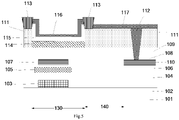
- Fig.1 luminous region 10 nonluminous transparent region 20 data line 21 cathode layer 11 base substrate 101 buffer layer 102 active layer 103 gate insulating layer 104 gate electrode 105 interlayer insulating layer 106 source/drain electrode 107 passivation layer 108 planarization layer 109 data line 110 pixel-defined layer 111 via hole 112 separating portion 113 anode 114 organic layer 115 first part of cathode layer 116 conductive unit 117 gate line 120 first region130 which emits light second region 140 which does not emit light power line150
- the present disclosure provides in embodiments an OLED array substrate according to the claims, including: a power line150, a gate line 120, a data line 110, and a plurality of pixel units 100 defined by the gate lines 120 and the data lines 110.
- Each pixel unit 100 includes: a first region 130 which emits light and a second region 140 which does not emit light.
- the first region 130 is provided with an organic light emitting diode (only a cathode 116 of the organic light emitting diode is shown in the drawings), and the second region 140 is provided with a conductive unit 117 which is connected in parallel with the data line 110 and arranged at the same layer with the cathode 116 of the organic light emitting diode.
- the power line150 is used to supply power to an anode of the organic light emitting diode.
- the conductive unit 117 arranged at the nonluminous region of the pixel unit 100, is connected in parallel with the data line 110. As a result, it is able to reduce a resistance of the data line 110, thereby to reduce an adverse effect caused by an IR drop on the organic light emitting diode.
- the pixel unit may further include a thin film transistor arranged at the first region 130 which emits light, connected to the organic light emitting diode, and configured to drive the organic light emitting diode to emit light.
- the OLED array substrate according to embodiments of the present disclosure may further include a pixel-defined layer.
- the data line 110 is connected in parallel with the conductive unit 117 through at least two via holes 112.
- the cathode 116 and the conductive unit 117 are arranged at the same layer and made of an identical material, usually a metal material.
- the cathode 116 and the conductive unit 117 may be made of a semitransparent metal material, so that the second region 140 which does not emit light is a semitransparent region, thereby to achieve transparent display.
- the cathode 116 and the conductive unit 117 may each be made of Ag, Mg or Al, or an alloy thereof, and they may each be of a height of 10 nm to 30 nm.
- the data line 110 may be made of a transparent metallic oxide, such as indium tin oxide (ITO) or indium zinc oxide (IZO).
- the data line made of the transparent metallic oxide may be arranged at the same layer with the anode of the organic light emitting diode.
- the anode is of a multi-layer structure including a metallic oxide layer and a metallic reflecting layer
- the data line may also be formed at the same time with the metallic oxide layer of the anode by a single patterning process.
- the data line may also be made of a metal material.
- the data line may be formed at the same time with a source/drain electrode of the thin film transistor by a single patterning process, i.e., the data line is made of a metal material identical to the source/drain electrode of the thin film transistor. At this time, the data line and the source/drain electrode of the thin film transistor are arranged at the same layer.
- the OLED array substrate may further include: a separating portion, through which the cathode 116 and the conductive unit 117 are insulated and separated from each other.
- the separating portion 113 is of a rectangle frame-like shape, and the conductive unit 117 is arranged within the separating portion 113, i.e., the conductive unit 117 is surrounded by the separating portion 113.
- the separating portion 113 is of a height greater than that of the cathode 116 and that of the conductive unit 117, and the separating portion 113 is of a height 2 ⁇ m to 5 ⁇ m greater than that of the cathode 116 and that of the conductive unit 117.
- the separating portion 113 may be formed prior to the formation of a cathode metal layer by an open mask (a co-layer metal mask) process.
- the cathode metal layer is of the height less than the separating portion 113, the metal layer can be insulated and separated by the separating portion 113, so that the cathode 116 of the organic light emitting diode is formed at the first region 130 of the pixel unit 100, and the conductive unit 117 is formed at the second region 140 of the pixel unit 100.
- the separating portion 113 is columnar and of a cross section in an inverted trapezoidal shape.
- the cathode and the conductive unit which are insulated and separated from each other may also be formed by a patterning process.
- the OLED array substrate includes:
- the thin film transistor of the pixel unit consists of the active layer 103, the gate insulating layer 104, the gate electrode 105, the interlayer insulating layer 106 and the source/drain electrode 107.
- the organic light emitting diode of the pixel unit consists of the anode 114, the organic layer 115 and the cathode 116.
- the thin film transistor is of a top-gate structure.
- the thin film transistor may also be of a bottom-gate structure.
- the present disclosure further provides in embodiments an OLED display device, including the above-mentioned OLED array substrate.
- the present disclosure further provides in embodiments a method for manufacturing an OLED array substrate according to the claims, including steps of forming a gate line and a data line, and forming a plurality of pixel units defined by the gate lines and the data lines.
- Each pixel unit includes a first region which emits light and a second region which does not emit light.
- the first region is provided with an organic light emitting diode
- the second region is provided with a conductive unit which is connected in parallel with the data line and arranged at the same layer with a cathode of the organic light emitting diode.
- the conductive unit arranged at the nonluminous region of the pixel unit, is connected in parallel with the data line. As a result, it is able to reduce the resistance of the data line, thereby to reduce the adverse effect caused by the IR drop on the organic light emitting diode.
- the step of forming the plurality of pixel units further includes:
- a part of the existing cathode layer is used to reduce the resistance of the data line. As a result, it is able to achieve the OLED array substrate in a simpler manner and reduce the production cost thereof
- the step of forming the plurality of pixel units includes:
- the data line may be made of a transparent metallic oxide.
- the step of forming the plurality of pixel units includes:
- the data line and the source/drain electrode of the thin film transistor are made of an identical metal material.
Landscapes
- Engineering & Computer Science (AREA)
- Microelectronics & Electronic Packaging (AREA)
- Electroluminescent Light Sources (AREA)
- Devices For Indicating Variable Information By Combining Individual Elements (AREA)
Claims (12)
- Substrat mit einem Array organischer Leuchtdioden (Organic Light Emitting Diode, OLED), umfassend: Gate-Leitungen (120), Datenleitungen (110) und mehrere Pixeleinheiten (100), die durch die Gate-Leitungen (120) und die Datenleitungen (110) definiert werden, wobei:jede Pixeleinheit (100) eine erste Region (130) umfasst, die Licht aussendet, und eine zweite Region (140) umfasst, die kein Licht aussendet,die erste Region (130) mit einer organischen Leuchtdiode versehen ist, die eine organische Schicht (115) umfasst; die zweite Region (140) mit einer leitfähigen Einheit (117) versehen ist, die zu einer entsprechenden Datenleitung (110) elektrisch parallel geschaltet ist, die Datenleitungen (110) und die leitfähige Einheit (117) in verschiedenen Schichten angeordnet sind;das OLED-Array-Substrat des Weiteren ein Basissubstrat (101) umfasst und eine orthografische Projektion der leitfähigen Einheit (117) auf das Basissubstrat (101) eine orthografische Projektion der organischen Schicht (115) auf das Substrat (10) nicht überlappt,dadurch gekennzeichnet, dass:
die leitfähige Einheit (117) in derselben Schicht wie eine Kathode (116) der organischen Leuchtdiode angeordnet ist. - OLED-Array-Substrat nach Anspruch 1, wobei die Datenleitung (110) über mindestens zwei Durchkontaktierungslöcher (112) zu der leitfähigen Einheit (117) parallel geschaltet ist.
- OLED-Array-Substrat nach Anspruch 1, des Weiteren umfassend einen Trennabschnitt (113), durch den die Kathode (116) von der leitfähigen Einheit (117) isoliert und getrennt ist.
- OLED-Array-Substrat nach Anspruch 3, wobei der Trennabschnitt (113) eine rechteckige, rahmenartige Form aufweist und die leitfähige Einheit (117) innerhalb des Trennabschnitts (113) angeordnet ist.
- OLED-Array-Substrat nach Anspruch 3, wobei der Trennabschnitt (113) eine größere Höhe als die Kathode (116) und die leitfähige Einheit (117) aufweist.
- OLED-Array-Substrat nach Anspruch 5, wobei der Trennabschnitt (113) eine Höhe aufweist, die 2 µm bis 5 µm größer ist als die der Kathode (116) und der leitfähigen Einheit (117).
- OLED-Array-Substrat nach Anspruch 5, wobei der Trennabschnitt (113) säulenförmig ist und einen Querschnitt in Form eines umgekehrten Trapezes aufweist.
- OLED-Array-Substrat nach Anspruch 1, wobei die leitfähige Einheit (117) und die Kathode (116) der organischen Leuchtdiode jeweils aus einem durchscheinenden Metallmaterial hergestellt sind.
- OLED-Array-Substrat nach Anspruch 8, wobei das durchscheinende Metallmaterial Ag, Mg oder Al oder eine Legierung davon ist.
- OLED-Array-Substrat nach Anspruch 1, wobei die leitfähige Einheit (117) und die Kathode (116) der OLED jeweils eine Höhe von 10 nm bis 30 nm aufweisen.
- Verfahren zur Herstellung eines Substrats mit einem Array organischer Leuchtdioden (Organic Light Emitting Diode, OLED) nach Anspruch 1, wobei das Verfahren die folgenden Schritte umfasst:
Bilden von Gate-Leitungen (120) und Datenleitungen (110), und Bilden mehrerer Pixeleinheiten (100), die durch die Gate-Leitungen (120) und die Datenleitungen (110) definiert werden, wobei:jede Pixeleinheit (100) eine erste Region (130) umfasst, die Licht aussendet, und eine zweite Region (140) umfasst, die kein Licht aussendet,die erste Region (130) mit einer OLED versehen ist, die eine organische Schicht (115) umfasst, unddie zweite Region (140) mit einer leitfähigen Einheit (117) versehen ist, die zu einer entsprechenden Datenleitung (110) elektrisch parallel geschaltet ist und auf einer selben Schicht mit einer Kathode (116) der OLED angeordnet ist,die Datenleitungen (110) und die leitfähige Einheit (117) in verschiedenen Schichten angeordnet sind;die leitfähige Einheit (117) und die Kathode (116) der organischen Leuchtdiode gleichzeitig im selben Prozess hergestellt werden,wobei der Schritt des Bildens der mehreren Pixeleinheiten umfasst: Bereitstellen eines Basissubstrats (101) des OLED-Array-Substrats und wobei eine orthographische Projektion der leitfähigen Einheit (117) auf das Basissubstrat (101) eine orthographische Projektion der organischen Schicht (115) auf das Substrat (101) nicht überlappt. - Verfahren nach Anspruch 11, wobei der Schritt des Bildens der mehreren Pixeleinheiten des Weiteren umfasst:Bilden einer Anode (114) der organischen Leuchtdiode und einer pixeldefinierten Schicht (111) auf dem Basissubstrat (101) und Bilden eines Durchkontaktierungslochs (112), das die pixeldefinierte Schicht (111) an einer Position, die der Datenleitung (110) entspricht, durchdringt;Bilden der organischen Schicht (115) der OLED auf der Anode (114);Bilden eines Trennabschnitts (113) auf der pixeldefinierten Schicht (111); undBilden einer Kathodenmetallschicht, die eine geringere Höhe als der Trennabschnitt (113) aufweist und durch den Trennabschnitt (113) in zwei Teile unterteilt wird, wobei ein Teil der Kathodenmetallschicht als die Kathode (116) der OLED dient und der andere Teil des Kathodenmetalls als die leitfähige Einheit (117) dient, die durch das Durchkontaktierungsloch (112) hindurch mit der Datenleitung (110) verbunden ist.
Priority Applications (1)
| Application Number | Priority Date | Filing Date | Title |
|---|---|---|---|
| EP21174026.1A EP3886174B1 (de) | 2014-09-23 | 2015-01-16 | Array-substrat einer organischen leuchtdiode, herstellungsverfahren dafür und anzeigevorrichtung |
Applications Claiming Priority (2)
| Application Number | Priority Date | Filing Date | Title |
|---|---|---|---|
| CN201410491588.5A CN104253148B (zh) | 2014-09-23 | 2014-09-23 | 一种有机发光二极管阵列基板及其制作方法、显示装置 |
| PCT/CN2015/070882 WO2016045269A1 (zh) | 2014-09-23 | 2015-01-16 | 有机发光二极管阵列基板及其制作方法、显示装置 |
Related Child Applications (2)
| Application Number | Title | Priority Date | Filing Date |
|---|---|---|---|
| EP21174026.1A Division EP3886174B1 (de) | 2014-09-23 | 2015-01-16 | Array-substrat einer organischen leuchtdiode, herstellungsverfahren dafür und anzeigevorrichtung |
| EP21174026.1A Division-Into EP3886174B1 (de) | 2014-09-23 | 2015-01-16 | Array-substrat einer organischen leuchtdiode, herstellungsverfahren dafür und anzeigevorrichtung |
Publications (3)
| Publication Number | Publication Date |
|---|---|
| EP3200232A1 EP3200232A1 (de) | 2017-08-02 |
| EP3200232A4 EP3200232A4 (de) | 2018-05-30 |
| EP3200232B1 true EP3200232B1 (de) | 2022-04-06 |
Family
ID=52187889
Family Applications (2)
| Application Number | Title | Priority Date | Filing Date |
|---|---|---|---|
| EP15729325.9A Active EP3200232B1 (de) | 2014-09-23 | 2015-01-16 | Organisches leuchtdioden-arraysubstrat und herstellungsverfahren dafür |
| EP21174026.1A Active EP3886174B1 (de) | 2014-09-23 | 2015-01-16 | Array-substrat einer organischen leuchtdiode, herstellungsverfahren dafür und anzeigevorrichtung |
Family Applications After (1)
| Application Number | Title | Priority Date | Filing Date |
|---|---|---|---|
| EP21174026.1A Active EP3886174B1 (de) | 2014-09-23 | 2015-01-16 | Array-substrat einer organischen leuchtdiode, herstellungsverfahren dafür und anzeigevorrichtung |
Country Status (4)
| Country | Link |
|---|---|
| US (1) | US9570533B2 (de) |
| EP (2) | EP3200232B1 (de) |
| CN (1) | CN104253148B (de) |
| WO (1) | WO2016045269A1 (de) |
Families Citing this family (15)
| Publication number | Priority date | Publication date | Assignee | Title |
|---|---|---|---|---|
| CN104253148B (zh) * | 2014-09-23 | 2017-08-25 | 京东方科技集团股份有限公司 | 一种有机发光二极管阵列基板及其制作方法、显示装置 |
| CN105914223B (zh) * | 2016-05-04 | 2019-08-13 | 上海天马有机发光显示技术有限公司 | 显示面板的制造方法和显示面板 |
| CN106654048B (zh) * | 2016-12-27 | 2019-01-25 | 武汉华星光电技术有限公司 | 顶发光型oled显示单元、制作方法及显示面板 |
| CN106653819B (zh) * | 2017-02-17 | 2020-02-14 | 京东方科技集团股份有限公司 | 阵列基板和显示装置 |
| CN107359274A (zh) * | 2017-06-27 | 2017-11-17 | 上海天马有机发光显示技术有限公司 | 显示面板、显示装置及显示面板的制作方法 |
| CN107579103B (zh) * | 2017-08-31 | 2025-01-21 | 京东方科技集团股份有限公司 | 一种阵列基板、显示面板、显示装置及其制作方法 |
| KR101938879B1 (ko) * | 2017-10-27 | 2019-01-15 | 엘지디스플레이 주식회사 | 표시장치 |
| KR102564720B1 (ko) * | 2018-04-17 | 2023-08-08 | 주식회사 디비하이텍 | 유기 발광 다이오드 표시 장치용 신호 제어 유닛, 이의 제조 방법 및 이를 포함하는 유기 발광 다이오드 소자 |
| CN110767166B (zh) * | 2018-10-31 | 2021-03-30 | 昆山国显光电有限公司 | 显示屏及显示终端 |
| CN110112176A (zh) * | 2019-03-18 | 2019-08-09 | 昆山国显光电有限公司 | 一种显示面板及显示装置 |
| WO2021217600A1 (zh) * | 2020-04-30 | 2021-11-04 | 京东方科技集团股份有限公司 | 镜面显示面板及其制作方法、显示装置 |
| CN111613616A (zh) * | 2020-06-02 | 2020-09-01 | 云谷(固安)科技有限公司 | 显示面板及显示装置 |
| CN113053969B (zh) * | 2021-03-10 | 2023-06-30 | 深圳市华星光电半导体显示技术有限公司 | 显示面板及显示装置 |
| CN113655620A (zh) * | 2021-08-25 | 2021-11-16 | 安徽熙泰智能科技有限公司 | 一种近眼显示眼镜 |
| CN114613827A (zh) * | 2022-03-14 | 2022-06-10 | 苏州清越光电科技股份有限公司 | 一种显示面板及其显示装置 |
Citations (1)
| Publication number | Priority date | Publication date | Assignee | Title |
|---|---|---|---|---|
| US20120169699A1 (en) * | 2011-01-04 | 2012-07-05 | Samsung Mobile Display Co., Ltd. | Organic luminescent display device and method of manufacturing the same |
Family Cites Families (16)
| Publication number | Priority date | Publication date | Assignee | Title |
|---|---|---|---|---|
| KR101151799B1 (ko) * | 2005-11-09 | 2012-06-01 | 엘지디스플레이 주식회사 | 액정표시장치용 어레이기판과 그 제조방법 |
| KR100765522B1 (ko) * | 2006-02-06 | 2007-10-10 | 엘지전자 주식회사 | 전계발광소자와 그 제조방법 |
| US7919352B2 (en) * | 2007-04-10 | 2011-04-05 | Global Oled Technology Llc | Electrical connection in OLED devices |
| KR100875102B1 (ko) * | 2007-09-03 | 2008-12-19 | 삼성모바일디스플레이주식회사 | 유기 발광 디스플레이 장치 |
| KR101699911B1 (ko) * | 2010-04-05 | 2017-01-26 | 삼성디스플레이 주식회사 | 유기 발광 표시 장치 |
| KR101058880B1 (ko) * | 2010-05-07 | 2011-08-25 | 서울대학교산학협력단 | 액티브 소자를 구비한 led 디스플레이 장치 및 그 제조방법 |
| KR20120019017A (ko) * | 2010-08-24 | 2012-03-06 | 삼성모바일디스플레이주식회사 | 유기 전계 발광 표시 장치 및 그 제조 방법 |
| CN102110685B (zh) * | 2010-11-05 | 2013-07-10 | 友达光电股份有限公司 | 像素结构以及显示面板 |
| KR101407587B1 (ko) * | 2011-06-02 | 2014-06-13 | 삼성디스플레이 주식회사 | 유기 발광 표시장치 및 그 제조방법 |
| US20130069067A1 (en) * | 2011-09-20 | 2013-03-21 | Keun Chun Youn | Organic light emitting diode (oled) display device and method for manufacturing the same |
| KR101884891B1 (ko) * | 2012-02-08 | 2018-08-31 | 삼성디스플레이 주식회사 | 표시 장치 |
| KR101931176B1 (ko) * | 2012-06-11 | 2018-12-21 | 삼성디스플레이 주식회사 | 유기 발광 표시장치 및 그 제조방법 |
| KR102020805B1 (ko) * | 2012-12-28 | 2019-09-11 | 엘지디스플레이 주식회사 | 투명 유기 발광 표시 장치 및 투명 유기 발광 표시 장치 제조 방법 |
| TWI523217B (zh) * | 2013-09-12 | 2016-02-21 | 友達光電股份有限公司 | 畫素結構 |
| CN109273516A (zh) | 2013-12-31 | 2019-01-25 | 京东方科技集团股份有限公司 | Amoled阵列基板及显示装置 |
| CN104253148B (zh) | 2014-09-23 | 2017-08-25 | 京东方科技集团股份有限公司 | 一种有机发光二极管阵列基板及其制作方法、显示装置 |
-
2014
- 2014-09-23 CN CN201410491588.5A patent/CN104253148B/zh active Active
-
2015
- 2015-01-16 WO PCT/CN2015/070882 patent/WO2016045269A1/zh not_active Ceased
- 2015-01-16 EP EP15729325.9A patent/EP3200232B1/de active Active
- 2015-01-16 EP EP21174026.1A patent/EP3886174B1/de active Active
- 2015-01-16 US US14/758,135 patent/US9570533B2/en active Active
Patent Citations (1)
| Publication number | Priority date | Publication date | Assignee | Title |
|---|---|---|---|---|
| US20120169699A1 (en) * | 2011-01-04 | 2012-07-05 | Samsung Mobile Display Co., Ltd. | Organic luminescent display device and method of manufacturing the same |
Also Published As
| Publication number | Publication date |
|---|---|
| CN104253148A (zh) | 2014-12-31 |
| EP3200232A1 (de) | 2017-08-02 |
| US20160254341A1 (en) | 2016-09-01 |
| WO2016045269A1 (zh) | 2016-03-31 |
| CN104253148B (zh) | 2017-08-25 |
| US9570533B2 (en) | 2017-02-14 |
| EP3886174B1 (de) | 2023-11-22 |
| EP3886174A1 (de) | 2021-09-29 |
| EP3200232A4 (de) | 2018-05-30 |
Similar Documents
| Publication | Publication Date | Title |
|---|---|---|
| EP3200232B1 (de) | Organisches leuchtdioden-arraysubstrat und herstellungsverfahren dafür | |
| KR102801694B1 (ko) | 유기 발광 표시 장치 및 그의 제조 방법 | |
| EP3680935B1 (de) | Arraysubstrat und anzeigevorrichtung | |
| US9972809B2 (en) | Array substrate, organic light-emitting diode display panel, and display device | |
| CN104752485B (zh) | 柔性显示装置及其制造方法 | |
| US9859349B2 (en) | Organic electroluminescent display substrate and manufacturing method thereof, and display device | |
| US8866706B2 (en) | Organic electroluminescent display device and manufacturing method of the same | |
| CN107785407B (zh) | 一种oled显示面板和显示装置 | |
| US9331301B2 (en) | Active matrix organic light-emitting display and display apparatus | |
| US11164918B2 (en) | Organic light emitting diode display panel having connection portion connecting organic light emitting diode to peripheral circuit and manufacturing method thereof | |
| KR20220068209A (ko) | 유기 발광 표시 장치 | |
| KR102278334B1 (ko) | 유기 발광 표시 장치 | |
| US10763319B2 (en) | Display panel, method for manufacturing the same, display device and displaying method | |
| CN104851893A (zh) | 一种阵列基板及其制备方法、显示装置 | |
| KR20150039440A (ko) | 유기 발광 디스플레이 장치 | |
| KR20140087914A (ko) | 유기전계발광표시장치 및 그 제조방법 | |
| KR20090094692A (ko) | 유기전계발광표시장치 | |
| KR20150001068A (ko) | 유기전계발광 표시장치 | |
| KR102740273B1 (ko) | 유기발광표시장치 | |
| KR102029169B1 (ko) | 디스플레이 장치와 이의 제조방법 | |
| KR20070027401A (ko) | 전계 발광 소자와 그 제조방법 |
Legal Events
| Date | Code | Title | Description |
|---|---|---|---|
| PUAI | Public reference made under article 153(3) epc to a published international application that has entered the european phase |
Free format text: ORIGINAL CODE: 0009012 |
|
| STAA | Information on the status of an ep patent application or granted ep patent |
Free format text: STATUS: REQUEST FOR EXAMINATION WAS MADE |
|
| 17P | Request for examination filed |
Effective date: 20150625 |
|
| AK | Designated contracting states |
Kind code of ref document: A1 Designated state(s): AL AT BE BG CH CY CZ DE DK EE ES FI FR GB GR HR HU IE IS IT LI LT LU LV MC MK MT NL NO PL PT RO RS SE SI SK SM TR |
|
| AX | Request for extension of the european patent |
Extension state: BA ME |
|
| DAX | Request for extension of the european patent (deleted) | ||
| A4 | Supplementary search report drawn up and despatched |
Effective date: 20180504 |
|
| RIC1 | Information provided on ipc code assigned before grant |
Ipc: H01L 27/32 20060101AFI20180426BHEP Ipc: H01L 51/52 20060101ALI20180426BHEP Ipc: H01L 23/50 20060101ALI20180426BHEP Ipc: H01L 51/56 20060101ALI20180426BHEP |
|
| STAA | Information on the status of an ep patent application or granted ep patent |
Free format text: STATUS: EXAMINATION IS IN PROGRESS |
|
| 17Q | First examination report despatched |
Effective date: 20200826 |
|
| RIC1 | Information provided on ipc code assigned before grant |
Ipc: H01L 51/52 20060101ALI20210901BHEP Ipc: H01L 27/32 20060101AFI20210901BHEP |
|
| GRAP | Despatch of communication of intention to grant a patent |
Free format text: ORIGINAL CODE: EPIDOSNIGR1 |
|
| STAA | Information on the status of an ep patent application or granted ep patent |
Free format text: STATUS: GRANT OF PATENT IS INTENDED |
|
| GRAJ | Information related to disapproval of communication of intention to grant by the applicant or resumption of examination proceedings by the epo deleted |
Free format text: ORIGINAL CODE: EPIDOSDIGR1 |
|
| GRAP | Despatch of communication of intention to grant a patent |
Free format text: ORIGINAL CODE: EPIDOSNIGR1 |
|
| INTG | Intention to grant announced |
Effective date: 20211011 |
|
| INTG | Intention to grant announced |
Effective date: 20211027 |
|
| GRAS | Grant fee paid |
Free format text: ORIGINAL CODE: EPIDOSNIGR3 |
|
| GRAA | (expected) grant |
Free format text: ORIGINAL CODE: 0009210 |
|
| STAA | Information on the status of an ep patent application or granted ep patent |
Free format text: STATUS: THE PATENT HAS BEEN GRANTED |
|
| AK | Designated contracting states |
Kind code of ref document: B1 Designated state(s): AL AT BE BG CH CY CZ DE DK EE ES FI FR GB GR HR HU IE IS IT LI LT LU LV MC MK MT NL NO PL PT RO RS SE SI SK SM TR |
|
| REG | Reference to a national code |
Ref country code: GB Ref legal event code: FG4D |
|
| REG | Reference to a national code |
Ref country code: CH Ref legal event code: EP |
|
| REG | Reference to a national code |
Ref country code: AT Ref legal event code: REF Ref document number: 1482214 Country of ref document: AT Kind code of ref document: T Effective date: 20220415 |
|
| REG | Reference to a national code |
Ref country code: IE Ref legal event code: FG4D |
|
| REG | Reference to a national code |
Ref country code: DE Ref legal event code: R096 Ref document number: 602015078028 Country of ref document: DE |
|
| REG | Reference to a national code |
Ref country code: LT Ref legal event code: MG9D |
|
| REG | Reference to a national code |
Ref country code: NL Ref legal event code: MP Effective date: 20220406 |
|
| REG | Reference to a national code |
Ref country code: AT Ref legal event code: MK05 Ref document number: 1482214 Country of ref document: AT Kind code of ref document: T Effective date: 20220406 |
|
| PG25 | Lapsed in a contracting state [announced via postgrant information from national office to epo] |
Ref country code: NL Free format text: LAPSE BECAUSE OF FAILURE TO SUBMIT A TRANSLATION OF THE DESCRIPTION OR TO PAY THE FEE WITHIN THE PRESCRIBED TIME-LIMIT Effective date: 20220406 |
|
| PG25 | Lapsed in a contracting state [announced via postgrant information from national office to epo] |
Ref country code: SE Free format text: LAPSE BECAUSE OF FAILURE TO SUBMIT A TRANSLATION OF THE DESCRIPTION OR TO PAY THE FEE WITHIN THE PRESCRIBED TIME-LIMIT Effective date: 20220406 Ref country code: PT Free format text: LAPSE BECAUSE OF FAILURE TO SUBMIT A TRANSLATION OF THE DESCRIPTION OR TO PAY THE FEE WITHIN THE PRESCRIBED TIME-LIMIT Effective date: 20220808 Ref country code: NO Free format text: LAPSE BECAUSE OF FAILURE TO SUBMIT A TRANSLATION OF THE DESCRIPTION OR TO PAY THE FEE WITHIN THE PRESCRIBED TIME-LIMIT Effective date: 20220706 Ref country code: LT Free format text: LAPSE BECAUSE OF FAILURE TO SUBMIT A TRANSLATION OF THE DESCRIPTION OR TO PAY THE FEE WITHIN THE PRESCRIBED TIME-LIMIT Effective date: 20220406 Ref country code: HR Free format text: LAPSE BECAUSE OF FAILURE TO SUBMIT A TRANSLATION OF THE DESCRIPTION OR TO PAY THE FEE WITHIN THE PRESCRIBED TIME-LIMIT Effective date: 20220406 Ref country code: GR Free format text: LAPSE BECAUSE OF FAILURE TO SUBMIT A TRANSLATION OF THE DESCRIPTION OR TO PAY THE FEE WITHIN THE PRESCRIBED TIME-LIMIT Effective date: 20220707 Ref country code: FI Free format text: LAPSE BECAUSE OF FAILURE TO SUBMIT A TRANSLATION OF THE DESCRIPTION OR TO PAY THE FEE WITHIN THE PRESCRIBED TIME-LIMIT Effective date: 20220406 Ref country code: ES Free format text: LAPSE BECAUSE OF FAILURE TO SUBMIT A TRANSLATION OF THE DESCRIPTION OR TO PAY THE FEE WITHIN THE PRESCRIBED TIME-LIMIT Effective date: 20220406 Ref country code: BG Free format text: LAPSE BECAUSE OF FAILURE TO SUBMIT A TRANSLATION OF THE DESCRIPTION OR TO PAY THE FEE WITHIN THE PRESCRIBED TIME-LIMIT Effective date: 20220706 Ref country code: AT Free format text: LAPSE BECAUSE OF FAILURE TO SUBMIT A TRANSLATION OF THE DESCRIPTION OR TO PAY THE FEE WITHIN THE PRESCRIBED TIME-LIMIT Effective date: 20220406 |
|
| REG | Reference to a national code |
Ref country code: DE Ref legal event code: R079 Ref document number: 602015078028 Country of ref document: DE Free format text: PREVIOUS MAIN CLASS: H01L0027320000 Ipc: H10K0059000000 |
|
| PG25 | Lapsed in a contracting state [announced via postgrant information from national office to epo] |
Ref country code: RS Free format text: LAPSE BECAUSE OF FAILURE TO SUBMIT A TRANSLATION OF THE DESCRIPTION OR TO PAY THE FEE WITHIN THE PRESCRIBED TIME-LIMIT Effective date: 20220406 Ref country code: PL Free format text: LAPSE BECAUSE OF FAILURE TO SUBMIT A TRANSLATION OF THE DESCRIPTION OR TO PAY THE FEE WITHIN THE PRESCRIBED TIME-LIMIT Effective date: 20220406 Ref country code: LV Free format text: LAPSE BECAUSE OF FAILURE TO SUBMIT A TRANSLATION OF THE DESCRIPTION OR TO PAY THE FEE WITHIN THE PRESCRIBED TIME-LIMIT Effective date: 20220406 Ref country code: IS Free format text: LAPSE BECAUSE OF FAILURE TO SUBMIT A TRANSLATION OF THE DESCRIPTION OR TO PAY THE FEE WITHIN THE PRESCRIBED TIME-LIMIT Effective date: 20220806 |
|
| REG | Reference to a national code |
Ref country code: DE Ref legal event code: R097 Ref document number: 602015078028 Country of ref document: DE |
|
| PG25 | Lapsed in a contracting state [announced via postgrant information from national office to epo] |
Ref country code: SM Free format text: LAPSE BECAUSE OF FAILURE TO SUBMIT A TRANSLATION OF THE DESCRIPTION OR TO PAY THE FEE WITHIN THE PRESCRIBED TIME-LIMIT Effective date: 20220406 Ref country code: SK Free format text: LAPSE BECAUSE OF FAILURE TO SUBMIT A TRANSLATION OF THE DESCRIPTION OR TO PAY THE FEE WITHIN THE PRESCRIBED TIME-LIMIT Effective date: 20220406 Ref country code: RO Free format text: LAPSE BECAUSE OF FAILURE TO SUBMIT A TRANSLATION OF THE DESCRIPTION OR TO PAY THE FEE WITHIN THE PRESCRIBED TIME-LIMIT Effective date: 20220406 Ref country code: EE Free format text: LAPSE BECAUSE OF FAILURE TO SUBMIT A TRANSLATION OF THE DESCRIPTION OR TO PAY THE FEE WITHIN THE PRESCRIBED TIME-LIMIT Effective date: 20220406 Ref country code: DK Free format text: LAPSE BECAUSE OF FAILURE TO SUBMIT A TRANSLATION OF THE DESCRIPTION OR TO PAY THE FEE WITHIN THE PRESCRIBED TIME-LIMIT Effective date: 20220406 Ref country code: CZ Free format text: LAPSE BECAUSE OF FAILURE TO SUBMIT A TRANSLATION OF THE DESCRIPTION OR TO PAY THE FEE WITHIN THE PRESCRIBED TIME-LIMIT Effective date: 20220406 |
|
| PLBE | No opposition filed within time limit |
Free format text: ORIGINAL CODE: 0009261 |
|
| STAA | Information on the status of an ep patent application or granted ep patent |
Free format text: STATUS: NO OPPOSITION FILED WITHIN TIME LIMIT |
|
| 26N | No opposition filed |
Effective date: 20230110 |
|
| PG25 | Lapsed in a contracting state [announced via postgrant information from national office to epo] |
Ref country code: AL Free format text: LAPSE BECAUSE OF FAILURE TO SUBMIT A TRANSLATION OF THE DESCRIPTION OR TO PAY THE FEE WITHIN THE PRESCRIBED TIME-LIMIT Effective date: 20220406 |
|
| PG25 | Lapsed in a contracting state [announced via postgrant information from national office to epo] |
Ref country code: SI Free format text: LAPSE BECAUSE OF FAILURE TO SUBMIT A TRANSLATION OF THE DESCRIPTION OR TO PAY THE FEE WITHIN THE PRESCRIBED TIME-LIMIT Effective date: 20220406 |
|
| REG | Reference to a national code |
Ref country code: CH Ref legal event code: PL |
|
| GBPC | Gb: european patent ceased through non-payment of renewal fee |
Effective date: 20230116 |
|
| PG25 | Lapsed in a contracting state [announced via postgrant information from national office to epo] |
Ref country code: LU Free format text: LAPSE BECAUSE OF NON-PAYMENT OF DUE FEES Effective date: 20230116 |
|
| REG | Reference to a national code |
Ref country code: BE Ref legal event code: MM Effective date: 20230131 |
|
| PG25 | Lapsed in a contracting state [announced via postgrant information from national office to epo] |
Ref country code: LI Free format text: LAPSE BECAUSE OF NON-PAYMENT OF DUE FEES Effective date: 20230131 Ref country code: GB Free format text: LAPSE BECAUSE OF NON-PAYMENT OF DUE FEES Effective date: 20230116 Ref country code: CH Free format text: LAPSE BECAUSE OF NON-PAYMENT OF DUE FEES Effective date: 20230131 |
|
| PG25 | Lapsed in a contracting state [announced via postgrant information from national office to epo] |
Ref country code: FR Free format text: LAPSE BECAUSE OF NON-PAYMENT OF DUE FEES Effective date: 20230131 Ref country code: BE Free format text: LAPSE BECAUSE OF NON-PAYMENT OF DUE FEES Effective date: 20230131 |
|
| PG25 | Lapsed in a contracting state [announced via postgrant information from national office to epo] |
Ref country code: IT Free format text: LAPSE BECAUSE OF FAILURE TO SUBMIT A TRANSLATION OF THE DESCRIPTION OR TO PAY THE FEE WITHIN THE PRESCRIBED TIME-LIMIT Effective date: 20220406 Ref country code: IE Free format text: LAPSE BECAUSE OF NON-PAYMENT OF DUE FEES Effective date: 20230116 |
|
| PG25 | Lapsed in a contracting state [announced via postgrant information from national office to epo] |
Ref country code: MC Free format text: LAPSE BECAUSE OF FAILURE TO SUBMIT A TRANSLATION OF THE DESCRIPTION OR TO PAY THE FEE WITHIN THE PRESCRIBED TIME-LIMIT Effective date: 20220406 |
|
| PG25 | Lapsed in a contracting state [announced via postgrant information from national office to epo] |
Ref country code: MC Free format text: LAPSE BECAUSE OF FAILURE TO SUBMIT A TRANSLATION OF THE DESCRIPTION OR TO PAY THE FEE WITHIN THE PRESCRIBED TIME-LIMIT Effective date: 20220406 |
|
| PG25 | Lapsed in a contracting state [announced via postgrant information from national office to epo] |
Ref country code: BG Free format text: LAPSE BECAUSE OF FAILURE TO SUBMIT A TRANSLATION OF THE DESCRIPTION OR TO PAY THE FEE WITHIN THE PRESCRIBED TIME-LIMIT Effective date: 20220406 |
|
| PG25 | Lapsed in a contracting state [announced via postgrant information from national office to epo] |
Ref country code: BG Free format text: LAPSE BECAUSE OF FAILURE TO SUBMIT A TRANSLATION OF THE DESCRIPTION OR TO PAY THE FEE WITHIN THE PRESCRIBED TIME-LIMIT Effective date: 20220406 |
|
| PG25 | Lapsed in a contracting state [announced via postgrant information from national office to epo] |
Ref country code: CY Free format text: LAPSE BECAUSE OF FAILURE TO SUBMIT A TRANSLATION OF THE DESCRIPTION OR TO PAY THE FEE WITHIN THE PRESCRIBED TIME-LIMIT; INVALID AB INITIO Effective date: 20150116 |
|
| PG25 | Lapsed in a contracting state [announced via postgrant information from national office to epo] |
Ref country code: HU Free format text: LAPSE BECAUSE OF FAILURE TO SUBMIT A TRANSLATION OF THE DESCRIPTION OR TO PAY THE FEE WITHIN THE PRESCRIBED TIME-LIMIT; INVALID AB INITIO Effective date: 20150116 |
|
| PG25 | Lapsed in a contracting state [announced via postgrant information from national office to epo] |
Ref country code: TR Free format text: LAPSE BECAUSE OF FAILURE TO SUBMIT A TRANSLATION OF THE DESCRIPTION OR TO PAY THE FEE WITHIN THE PRESCRIBED TIME-LIMIT Effective date: 20220406 |
|
| PGFP | Annual fee paid to national office [announced via postgrant information from national office to epo] |
Ref country code: DE Payment date: 20260121 Year of fee payment: 12 |