EP3200244B1 - Cellule solaire et module de cellule solaire - Google Patents
Cellule solaire et module de cellule solaire Download PDFInfo
- Publication number
- EP3200244B1 EP3200244B1 EP17153797.0A EP17153797A EP3200244B1 EP 3200244 B1 EP3200244 B1 EP 3200244B1 EP 17153797 A EP17153797 A EP 17153797A EP 3200244 B1 EP3200244 B1 EP 3200244B1
- Authority
- EP
- European Patent Office
- Prior art keywords
- amorphous silicon
- layer
- solar cell
- silicon layer
- silicon substrate
- Prior art date
- Legal status (The legal status is an assumption and is not a legal conclusion. Google has not performed a legal analysis and makes no representation as to the accuracy of the status listed.)
- Active
Links
Images


Classifications
-
- H—ELECTRICITY
- H10—SEMICONDUCTOR DEVICES; ELECTRIC SOLID-STATE DEVICES NOT OTHERWISE PROVIDED FOR
- H10F—INORGANIC SEMICONDUCTOR DEVICES SENSITIVE TO INFRARED RADIATION, LIGHT, ELECTROMAGNETIC RADIATION OF SHORTER WAVELENGTH OR CORPUSCULAR RADIATION
- H10F10/00—Individual photovoltaic cells, e.g. solar cells
- H10F10/10—Individual photovoltaic cells, e.g. solar cells having potential barriers
- H10F10/16—Photovoltaic cells having only PN heterojunction potential barriers
- H10F10/164—Photovoltaic cells having only PN heterojunction potential barriers comprising heterojunctions with Group IV materials, e.g. ITO/Si or GaAs/SiGe photovoltaic cells
- H10F10/165—Photovoltaic cells having only PN heterojunction potential barriers comprising heterojunctions with Group IV materials, e.g. ITO/Si or GaAs/SiGe photovoltaic cells the heterojunctions being Group IV-IV heterojunctions, e.g. Si/Ge, SiGe/Si or Si/SiC photovoltaic cells
- H10F10/166—Photovoltaic cells having only PN heterojunction potential barriers comprising heterojunctions with Group IV materials, e.g. ITO/Si or GaAs/SiGe photovoltaic cells the heterojunctions being Group IV-IV heterojunctions, e.g. Si/Ge, SiGe/Si or Si/SiC photovoltaic cells the Group IV-IV heterojunctions being heterojunctions of crystalline and amorphous materials, e.g. silicon heterojunction [SHJ] photovoltaic cells
-
- H—ELECTRICITY
- H10—SEMICONDUCTOR DEVICES; ELECTRIC SOLID-STATE DEVICES NOT OTHERWISE PROVIDED FOR
- H10F—INORGANIC SEMICONDUCTOR DEVICES SENSITIVE TO INFRARED RADIATION, LIGHT, ELECTROMAGNETIC RADIATION OF SHORTER WAVELENGTH OR CORPUSCULAR RADIATION
- H10F77/00—Constructional details of devices covered by this subclass
- H10F77/10—Semiconductor bodies
- H10F77/12—Active materials
-
- H—ELECTRICITY
- H10—SEMICONDUCTOR DEVICES; ELECTRIC SOLID-STATE DEVICES NOT OTHERWISE PROVIDED FOR
- H10F—INORGANIC SEMICONDUCTOR DEVICES SENSITIVE TO INFRARED RADIATION, LIGHT, ELECTROMAGNETIC RADIATION OF SHORTER WAVELENGTH OR CORPUSCULAR RADIATION
- H10F77/00—Constructional details of devices covered by this subclass
- H10F77/10—Semiconductor bodies
- H10F77/12—Active materials
- H10F77/122—Active materials comprising only Group IV materials
-
- H—ELECTRICITY
- H10—SEMICONDUCTOR DEVICES; ELECTRIC SOLID-STATE DEVICES NOT OTHERWISE PROVIDED FOR
- H10F—INORGANIC SEMICONDUCTOR DEVICES SENSITIVE TO INFRARED RADIATION, LIGHT, ELECTROMAGNETIC RADIATION OF SHORTER WAVELENGTH OR CORPUSCULAR RADIATION
- H10F77/00—Constructional details of devices covered by this subclass
- H10F77/10—Semiconductor bodies
- H10F77/16—Material structures, e.g. crystalline structures, film structures or crystal plane orientations
- H10F77/162—Non-monocrystalline materials, e.g. semiconductor particles embedded in insulating materials
- H10F77/166—Amorphous semiconductors
-
- H—ELECTRICITY
- H10—SEMICONDUCTOR DEVICES; ELECTRIC SOLID-STATE DEVICES NOT OTHERWISE PROVIDED FOR
- H10F—INORGANIC SEMICONDUCTOR DEVICES SENSITIVE TO INFRARED RADIATION, LIGHT, ELECTROMAGNETIC RADIATION OF SHORTER WAVELENGTH OR CORPUSCULAR RADIATION
- H10F77/00—Constructional details of devices covered by this subclass
- H10F77/50—Encapsulations or containers
-
- H—ELECTRICITY
- H10—SEMICONDUCTOR DEVICES; ELECTRIC SOLID-STATE DEVICES NOT OTHERWISE PROVIDED FOR
- H10F—INORGANIC SEMICONDUCTOR DEVICES SENSITIVE TO INFRARED RADIATION, LIGHT, ELECTROMAGNETIC RADIATION OF SHORTER WAVELENGTH OR CORPUSCULAR RADIATION
- H10F19/00—Integrated devices, or assemblies of multiple devices, comprising at least one photovoltaic cell covered by group H10F10/00, e.g. photovoltaic modules
- H10F19/80—Encapsulations or containers for integrated devices, or assemblies of multiple devices, having photovoltaic cells
-
- H—ELECTRICITY
- H10—SEMICONDUCTOR DEVICES; ELECTRIC SOLID-STATE DEVICES NOT OTHERWISE PROVIDED FOR
- H10F—INORGANIC SEMICONDUCTOR DEVICES SENSITIVE TO INFRARED RADIATION, LIGHT, ELECTROMAGNETIC RADIATION OF SHORTER WAVELENGTH OR CORPUSCULAR RADIATION
- H10F77/00—Constructional details of devices covered by this subclass
- H10F77/20—Electrodes
- H10F77/244—Electrodes made of transparent conductive layers, e.g. transparent conductive oxide [TCO] layers
-
- Y—GENERAL TAGGING OF NEW TECHNOLOGICAL DEVELOPMENTS; GENERAL TAGGING OF CROSS-SECTIONAL TECHNOLOGIES SPANNING OVER SEVERAL SECTIONS OF THE IPC; TECHNICAL SUBJECTS COVERED BY FORMER USPC CROSS-REFERENCE ART COLLECTIONS [XRACs] AND DIGESTS
- Y02—TECHNOLOGIES OR APPLICATIONS FOR MITIGATION OR ADAPTATION AGAINST CLIMATE CHANGE
- Y02E—REDUCTION OF GREENHOUSE GAS [GHG] EMISSIONS, RELATED TO ENERGY GENERATION, TRANSMISSION OR DISTRIBUTION
- Y02E10/00—Energy generation through renewable energy sources
- Y02E10/50—Photovoltaic [PV] energy
-
- Y—GENERAL TAGGING OF NEW TECHNOLOGICAL DEVELOPMENTS; GENERAL TAGGING OF CROSS-SECTIONAL TECHNOLOGIES SPANNING OVER SEVERAL SECTIONS OF THE IPC; TECHNICAL SUBJECTS COVERED BY FORMER USPC CROSS-REFERENCE ART COLLECTIONS [XRACs] AND DIGESTS
- Y02—TECHNOLOGIES OR APPLICATIONS FOR MITIGATION OR ADAPTATION AGAINST CLIMATE CHANGE
- Y02E—REDUCTION OF GREENHOUSE GAS [GHG] EMISSIONS, RELATED TO ENERGY GENERATION, TRANSMISSION OR DISTRIBUTION
- Y02E10/00—Energy generation through renewable energy sources
- Y02E10/50—Photovoltaic [PV] energy
- Y02E10/547—Monocrystalline silicon PV cells
-
- Y—GENERAL TAGGING OF NEW TECHNOLOGICAL DEVELOPMENTS; GENERAL TAGGING OF CROSS-SECTIONAL TECHNOLOGIES SPANNING OVER SEVERAL SECTIONS OF THE IPC; TECHNICAL SUBJECTS COVERED BY FORMER USPC CROSS-REFERENCE ART COLLECTIONS [XRACs] AND DIGESTS
- Y02—TECHNOLOGIES OR APPLICATIONS FOR MITIGATION OR ADAPTATION AGAINST CLIMATE CHANGE
- Y02E—REDUCTION OF GREENHOUSE GAS [GHG] EMISSIONS, RELATED TO ENERGY GENERATION, TRANSMISSION OR DISTRIBUTION
- Y02E10/00—Energy generation through renewable energy sources
- Y02E10/50—Photovoltaic [PV] energy
- Y02E10/548—Amorphous silicon PV cells
Definitions
- the present invention relates to a solar cell and a solar cell module.
- Hybrid solar cells having a heterojunction structure of a crystalline semiconductor substrate and an amorphous semiconductor thin film are in practical use.
- Patent Literature (PTL) 1 discloses a photovoltaic device which improves interface characteristics between a crystalline semiconductor substrate and an amorphous semiconductor thin film to improve photoelectric conversion characteristics. Specifically, in the photovoltaic device disclosed by PTL 1, a p-type amorphous silicon thin film is laminated above a first principal surface of an n-type single-crystal silicon substrate with a first i-type amorphous silicon thin film being between the n-type single-crystal silicon substrate and the p-type amorphous silicon thin film.
- an n-type amorphous silicon thin film is laminated above a second principal surface of the n-type single-crystal silicon substrate with a second i-type amorphous silicon thin film being between the n-type single-crystal silicon substrate and the n-type amorphous silicon thin film.
- the second i-type amorphous silicon layer is formed after the second principal surface of the single-crystal silicon substrate is plasma-treated by plasma discharge using a mixed gas of a hydrogen gas and a gas including phosphorus on the second principal surface of the single-crystal silicon substrate. With this, phosphorus is introduced into an interface between the single-crystal silicon substrate and the second i-type amorphous silicon layer.
- the above configuration makes it possible to reduce recombination of charge carriers in a semiconductor junction interface between the crystalline semiconductor substrate and the amorphous semiconductor thin film, improve junction characteristics, and to improve the photoelectric conversion characteristics of open-circuit voltage (Voc) etc.
- US 2015/280031 A1 discloses a solar cell comprising a silicon substrate which is crystalline; a first silicon oxide layer which is disposed on a first principal surface of the silicon substrate and includes phosphorus as an impurity; and a first amorphous silicon layer which is disposed on the first silicon oxide layer.
- an object of the present invention is to provide a solar cell having improved photoelectric conversion characteristics and a heterojunction structure, and a solar cell module.
- a solar cell includes: a silicon substrate which is crystalline; a first silicon oxide layer which is disposed on a first principal surface of the silicon substrate and includes phosphorus as an impurity; and a first amorphous silicon layer disposed on the first silicon oxide layer, wherein a phosphorous concentration profile in a thickness direction between the first amorphous silicon layer and the silicon substrate has a maximum value in the first silicon oxide layer.
- the silicon oxide layer including phosphorus as the impurity is between the silicon substrate which is crystalline and the amorphous silicon layer in the solar cell or solar cell module according to one aspect of the present invention. Consequently, it is possible to provide the solar cell with improved photoelectric conversion or the solar cell module with improved power generation efficiency.
- a "front surface” of a solar cell denotes a surface which more light can enter inwardly in comparison to a "back surface” which is a surface opposite the front surface (at least 50 to 100% of light enters inwardly from the front surface).
- Examples of the front surface include a surface which no light enters inwardly from a "back surface” side.
- a "front surface” of a solar cell module denotes a surface which light on a side opposite the "front surface” of the solar cell can enter, and a "back surface” of the solar cell module denotes a surface opposite the front surface of the solar cell module.
- an expression such as “provide a second member on a first member” is not intended only for a case where the first and second members are provided in direct contact with each other. In other words, examples of this expression include a case where another member is between the first and second members. It is also to be noted that regarding the expression “substantially XX,” for example, “substantially the same” is intended to include not only exactly the same but also something that can be substantially recognized as the same.
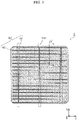
- FIG. 1 An exemplary plane configuration of a solar cell module according to the embodiment will be described with reference to FIG. 1 .
- FIG. 1 is a schematic plan view of solar cell module 100 according to the embodiment.
- FIG. 2 is a structural cross-sectional view of solar cell module 100 according to the embodiment, in a column direction. Specifically, FIG. 2 is a II-II cross-sectional view of solar cell module 100 illustrated by FIG. 1 .
- solar cell module 100 includes solar cells 1, tab lines 120, connecting lines 130, and frame 150.
- solar cell module 100 further includes front surface encapsulant member 170A, back surface encapsulant member 170B, front surface protective member 180A, and back surface protective member 180B.
- Solar cells 1 are planar photovoltaic elements which are arranged in a matrix on a light-receiving surface and generate electric power in response to light irradiation.
- Tab lines 120 each are a line member which is disposed on a front surface of solar cell 1 and electrically connects solar cells 1 neighboring in the column direction.
- Tab line 120 is a ribbon metal foil, for example.
- Tab line 120 can be produced, for example, by cutting, into strips having a predetermined length, a metal foil such as a copper foil and a silver foil whose entire surface is covered with solder, silver, etc.
- Connecting lines 130 each are a line member connecting solar cell strings. It is to be noted that the solar cell strings each are an aggregate of solar cells 1 arranged in the column direction and connected by tab line 120.
- Frame 150 is an outer frame member which covers an outer periphery of a panel on which solar cells 1 are two-dimensionally arrayed.
- a light diffusion member may be disposed between neighboring solar cells 1. With this, light entering a gap region between solar cells 1 can be redistributed to solar cells 1, and thus light gathering efficiency of solar cells 1 is increased. Accordingly, it is possible to increase overall photoelectric conversion efficiency of the solar cell module.
- tab line 120 disposed on a front surface of one of solar cells 1 is also disposed on a back surface of the other of solar cells 1. More specifically, a back surface at one end portion of tab line 120 is bonded to a bus bar electrode on the front surface of the one of solar cells 1, and a front surface at the other end portion of table line 120 is bonded to a bus bar electrode on the back surface of the other of solar cells 1.
- Tab line 120 and the bus bar electrode are bonded with an electrically conductive adhesive, for example.
- the electrically conductive adhesive include a conductive adhesive paste, a conductive adhesive film, and an anisotropic conductive film.
- the electrically conductive adhesive paste is, for example, a paste adhesive produced by dispersing conductive particles into a thermosetting adhesive resin material such as an epoxy resin, an acryl resin, and a urethane resin.
- the electrically conductive adhesive film and the anisotropic conductive film each are a film adhesive produced by dispersing conductive particles into a thermosetting adhesive resin material.
- the aforementioned electrically conductive adhesive may be a solder material.
- a resin adhesive including no conductive particle may be used instead of the electrically conductive adhesive.
- properly designing an application thickness for the resin adhesive allows the resin adhesive to soften when pressure is applied at the time of thermal compression bonding, and the bus bar electrode and tab line 120 to be electrically connected in direct contact with each other.
- front surface protective member 180A is provided on a front surface side of solar cells 1
- back surface protective member 180B is provided on a back surface side of solar cells 1.
- Front surface encapsulant member 170A is disposed between a surface including solar cells 1 and front surface protective member 180A
- back surface encapsulant member 170B is disposed between a surface including solar cells 1 and back surface protective member 180B.
- Front surface protective member 180A and back surface protective member 180B are fixed by front surface encapsulant member 170A and back surface encapsulant member 170B, respectively.
- Front surface protective member 180A is a translucent substrate which protects a front surface side of solar cell module 100, and protects the inside (solar cells 1 etc.) of solar cell module 100 from an external environment such as wind and rain, external shock, and fire.
- Front surface protective member 180A is a translucent member having translucency, and is a glass substrate (transparent glass substrate) including a transparent glass material or a resin substrate including a film-like or plate-like hard resin material having translucency and impermeability, for example.
- Back surface protective member 180B is a member which protects a back surface of solar cell module 100 and includes, for example, a resin film such as polyethylene terephthalate or a laminated film having a structure in which an Al foil is disposed between resin films.
- Front surface encapsulant member 170A and back surface encapsulant member 170B have a sealing function for isolating solar cells 1 from the external environment. Disposing front surface encapsulant member 170A and back surface encapsulant member 170B makes it possible to ensure high heat resistance and high humidity resistance of solar cell module 1 to be installed outdoors.
- Front surface encapsulant member 170A and back surface encapsulant member 170B each include a translucent polymer material having a sealing function.
- Examples of the polymer material of front surface encapsulant member 170A include a translucent resin material such as ethylene-vinyl acetate (EVA).
- EVA ethylene-vinyl acetate
- front surface encapsulant member 170A and back surface encapsulant member 170B may include the same material.
- each solar cell 1 which is a main component of solar cell module 100.
- FIG. 3 is a plan view of solar cell 1 according to the embodiment. As illustrated by the figure, solar cell 1 is substantially square in a plan view. Solar cell 1 has a size of 125 mm in length ⁇ 125 mm in width ⁇ 200 ⁇ m in thickness, for example. Moreover, on a surface of solar cell 1, bus bar electrodes 42 having a stripe shape are formed in parallel to each other, and finger electrodes 41 having a stripe shape are formed in parallel to each other to cross bus bar electrodes 42 at right angles. Bus bar electrodes 42 and finger electrodes 41 constitute collector electrode 43. Collector electrode 43 is formed using, for example, a conductive paste including conductive particles such as Ag (silver).
- bus bar electrodes 42 for example, a line width of bus bar electrodes 42 is 1.5 mm, a line width of finger electrodes 41 is 100 ⁇ m, and a pitch of finger electrodes 41 is 2 mm. Furthermore, tab lines 120 are bonded onto bus bar electrodes 42.
- FIG. 4 is a schematic cross-sectional view illustrating a laminated structure of solar cell 1 according to the embodiment. It is to be noted that this figure is a IV-IV cross-sectional view of solar cell 1 illustrated by FIG. 3 .
- solar cell 1 includes silicon substrate 10, P-doped silicon oxide layer 20, amorphous silicon layers 30 and 60, transparent electrodes 40 and 70, and finger electrodes 41 and 71. It is to be noted that FIG. 4 illustrates only finger electrode 41 included in collector electrode 43.
- Silicon substrate 10 is an n-type single-crystal silicon substrate having a first principal surface and a second principal surface which are back to back with each other. It is to be noted that silicon substrate 10 may include polysilicon. Moreover, the first principal surface and the second principal surface each may have a textured structure in which pyramids are two-dimensionally arranged. Furthermore, silicon substrate 10 has an n-type dopant concentration of at least 3 ⁇ 10 14 /cm 3 and at most 9.1 ⁇ 10 15 /cm 3 , for example, and a resistivity of at least 0.5 ⁇ cm and at most 15 ⁇ cm, for example.
- silicon substrate 10 in order to further reduce recombination of charge carriers in silicon substrate 10, silicon substrate 10 preferably has an n-type dopant concentration of at most 3 ⁇ 10 15 /cm 3 , and a resistivity of at least 1.5 ⁇ cm. Additionally, in order to reduce output loss caused by series resistance, silicon substrate 10 preferably has an n-type dopant concentration of at least 3.5 ⁇ 10 1 4/cm 3 , and a resistivity of at most 13 ⁇ cm.
- P-doped silicon oxide layer 20 is a first silicon oxide layer disposed on the first principal surface of silicon substrate 10, and includes a silicon oxide film including phosphorus as an impurity.
- P-doped silicon oxide layer 20 has a thickness of at least 0.1 nm and at most 3 nm, for example.
- P-doped silicon oxide layer 20 more preferably has a thickness of at most 2 nm.
- P-doped silicon oxide layer 20 is thinner than dielectric layer 31 and n-type amorphous silicon layer 32 which will be described later.
- P-doped silicon oxide layer 20 may be formed into an island shape, in an interface between silicon substrate 10 and amorphous silicon layer 30.
- P-doped silicon oxide layer 20 has a phosphorus concentration of at least 1 ⁇ 10 19 /cm 3 and at most 5 ⁇ 10 20 /cm 3 , and an oxygen atomic concentration of at least 1 ⁇ 10 21 /cm 3 and at most 2 ⁇ 10 22 /cm 3 .
- P-doped silicon oxide layer 20 more preferably has a phosphorus concentration of at least 5 ⁇ 10 19 /cm 3 and at most 1 ⁇ 10 20 /cm 3 , and an oxygen atomic concentration of at least 2 ⁇ 10 21 /cm 3 and at most 5 ⁇ 10 21 /cm 3 .
- P-doped silicon oxide layer 20 may be an amorphous layer. In such a case, P-doped silicon oxide layer 20 can be formed at low temperature of at most 200 °C, for example.
- Amorphous silicon layer 30 is a first amorphous silicon layer which is formed on a front surface of P-doped silicon oxide layer 20 and is substantially in an amorphous state.
- Amorphous silicon layer 30 includes dielectric layer 31 and n-type amorphous silicon layer 32.
- Dielectric layer 31 is a first dielectric layer formed on the front surface of P-doped silicon oxide layer 20, and is, for example, a first intrinsic amorphous silicon layer which includes hydrogen and is in the amorphous state.
- an intrinsic amorphous silicon layer denotes an amorphous semiconductor layer having an included p-type or n-type dopant concentration of at most 5 ⁇ 10 18 /cm 3 or an amorphous semiconductor layer having, in a case where both p-type and n-type dopants are included, a difference between a p-type dopant concentration and an n-type dopant concentration which is at most 5 ⁇ 10 18 /cm 3 .
- Dielectric layer 31 may be made thin to reduce absorption of light as much as possible, and at the same time may be made thick to sufficiently passivate a front surface of silicon substrate 10.
- Dielectric layer 31 has, for example, a film thickness of at least 1 nm and at most 25 nm, and preferably has a film thickness of at least 5 nm and at most 10 nm.
- dielectric layer 31 may not be the intrinsic amorphous silicon layer as described above, and may be a silicon oxide layer, a silicon nitride layer, or an aluminum oxide layer. Moreover, dielectric layer 31 may not be present, and n-type amorphous silicon layer 32 may be directly formed on the front surface of P-doped silicon oxide layer 20.
- N-type amorphous silicon layer 32 is a first conductive amorphous silicon layer which is formed on dielectric layer 31, includes dopants of n-type which is the same as a conductivity type of silicon substrate 10, and is substantially in the amorphous state.
- N-type amorphous silicon layer 32 includes, for example, an amorphous silicon semiconductor thin film including hydrogen.
- N-type amorphous silicon layer 32 has a higher n-type dopant concentration in a film than dielectric layer 31, and preferably has an n-type dopant concentration of at least 1 ⁇ 10 20 /cm 3 .
- Examples of the dopants of n-type include phosphorus (P).
- N-type amorphous silicon layer 32 may be made thin to reduce absorption of light as much as possible, and at the same time may be made thick to effectively separate charge carriers generated in silicon substrate 10 and to allow transparent electrode 40 to efficiently collect the generated charge carriers. It is to be noted that n-type amorphous silicon layer 32 has the n-type dopant concentration which may gradually change from a side of P-doped silicon oxide layer 20 to a side of transparent electrode 40.
- Amorphous silicon layer 60 is a second amorphous silicon layer which is disposed on the second principal surface of silicon substrate 10 and is substantially in the amorphous state.
- Amorphous silicon layer 60 includes dielectric layer 61 and p-type amorphous silicon layer 62.
- Dielectric layer 61 is a second dielectric layer formed on the second principal surface of silicon substrate 10, and is, for example, a second intrinsic amorphous silicon layer which includes hydrogen and is in the amorphous state. Like dielectric layer 31, dielectric layer 61 has, for example, a film thickness of at least 1 nm and at most 25 nm, and preferably has a film thickness of at least 5 nm and at most 10 nm.
- dielectric layer 61 may not be the intrinsic amorphous silicon layer as described above, and may be a silicon oxide layer, a silicon nitride layer, or an aluminum oxide layer. In addition, dielectric layer 61 may not be present, and p-type amorphous silicon layer 62 may be directly formed on the second principal surface of silicon substrate 10.
- P-type amorphous silicon layer 62 is a second conductive amorphous silicon layer which is formed on dielectric layer 61, includes dopants of p-type which is opposite of a conductivity type of silicon substrate 10, and is substantially in the amorphous state.
- P-type amorphous silicon layer 62 includes, for example, an amorphous silicon semiconductor thin film including hydrogen.
- P-type amorphous silicon layer 62 has a higher p-type dopant concentration in a film than dielectric layer 61, and preferably has a p-type dopant concentration of at least 1 ⁇ 10 20 /cm 3 . Examples of the dopants of p-type include boron (B).
- P-type amorphous silicon layer 62 may be made thin to reduce absorption of light as much as possible, and at the same time may be made thick to effectively separate charge carriers generated in silicon substrate 10 and to allow transparent electrode 70 to efficiently collect the generated charge carriers. It is to be noted that p-type amorphous silicon layer 62 has the p-type dopant concentration which may gradually change from a side of silicon substrate 10 to a side of transparent electrode 70.
- amorphous silicon layer 30, amorphous silicon layer 60, n-type amorphous silicon layer 32, and p-type amorphous silicon layer 62 each may include a microcrystal.
- Transparent electrode 40 is formed on a front surface of amorphous silicon layer 30, and collects charge carriers in n-type amorphous silicon layer 32.
- transparent electrode 70 is formed on a back surface of amorphous silicon layer 60, and collects charge carriers in p-type amorphous silicon layer 62.
- Transparent electrodes 40 and 70 each include, for example, a transparent conductive oxide such as an indium tin oxide (ITO).
- the conductivity type of silicon substrate 10 is the n-type in the embodiment, the conductivity type of silicon substrate 10 may be the p-type.
- p-type amorphous silicon layer 62 of amorphous silicon layer 60 has the same conductivity type as the conductivity type of silicon substrate 10, and thus amorphous silicon layer 60 is the first amorphous silicon layer.
- n-type amorphous silicon layer 32 of amorphous silicon layer 30 has a conductivity type opposite of the conductivity type of silicon substrate 10, and thus amorphous silicon layer 30 is the second amorphous silicon layer.
- solar cell 1 is a bifacial solar cell including transparent electrode 70 disposed also on a side of a second principal surface
- solar cell 1 may be an unifacial solar cell including, instead of transparent electrode 70, a metal electrode which is not transparent.
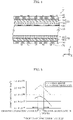
- FIG. 5 is a graph illustrating concentration profiles of oxygen and phosphorus with respect to a depth direction from amorphous silicon layer 30 to silicon substrate 10.
- concentrations of oxygen and phosphorus are measured by secondary ion mass spectroscopy (SIMS) in a direction (depth direction) from amorphous silicon layer 30 to silicon substrate 10.
- SIMS secondary ion mass spectroscopy
- a silicon oxide layer including phosphorus as an impurity is between amorphous silicon layer 30 and silicon substrate 10.
- P-doped silicon oxide layer 20 has the phosphorus atomic concentration of at least 1 ⁇ 10 19 /cm 3 and at most 5 ⁇ 10 20 /cm 3 , and the oxygen atomic concentration of at least 1 ⁇ 10 21 /cm 3 and at most 2 ⁇ 10 22 /cm 3 .
- the recombination of the charge carriers in the amorphous silicon layer is increased. Furthermore, recombination via excessive impurities in the amorphous silicon layer is accelerated. In other words, the recombination of the charge carriers in the amorphous silicon layer cannot be completely reduced by merely introducing the impurity into the front surface of the silicon substrate. In addition, a concentration of excessive impurities in the front surface of the silicon substrate increases the defects in the front surface of the silicon substrate, and thus the photoelectric conversion characteristics are deteriorated.
- the silicon oxide layer is disposed between amorphous silicon layer 30 and silicon substrate 10, and phosphorus is doped into the silicon oxide layer.
- P-doped silicon oxide layer 20 including phosphorus as the impurity is disposed between amorphous silicon layer 30 and silicon substrate 10.
- amorphous silicon layer 30 In order to improve an open-circuit voltage, it is important to maintain a high degree of amorphousness of amorphous silicon layer 30 in addition to reducing recombination of charge carriers caused by impurity doping. From this point of view, disposing the silicon oxide layer between amorphous silicon layer 30 and silicon substrate 10 makes it possible to suppress, in amorphous silicon layer 30, epitaxial growth reflecting crystallinity of silicon substrate 10. Moreover, instead of an impurity, P-doped silicon oxide layer 20 is disposed in the junction interface, and thus it is possible to reduce the increasing of the defects in the front surface of silicon substrate 10. With this, it is possible to improve the open-circuit voltage.
- disposing the silicon oxide layer including phosphorus as the impurity between amorphous silicon layer 30 and silicon substrate 10 makes it possible to reduce the recombination of the charge carriers in the interface and suppress the epitaxial growth in amorphous silicon layer 30. Accordingly, since it is possible to ameliorate field effect, the improvement of the open-circuit voltage which cannot be achieved by merely doping impurity elements into the silicon substrate can be achieved, or it is possible to improve the open-circuit voltage without degrading photoelectric conversion performance which depends on the defects in the front surface of the silicon substrate.
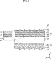
- FIG. 6 is a schematic cross-sectional view illustrating a laminated structure of solar cell 1A according to a variation of the embodiment.
- solar cell 1A according to the variation differs from solar cell 1 according to the embodiment in that diffusion region 10a of phosphorus is in a front surface (first principal surface) of silicon substrate 10.
- silicon substrate 10 has, in the first principal surface, diffusion region 10a including phosphorus as an impurity.
- diffusion region 10a has a phosphorus atomic concentration lower than a phosphorus atomic concentration of p-doped silicon oxide layer 20.
- diffusion region 10a has, for example, a phosphorus atomic concentration of at least 5 ⁇ 10 16 /cm 3 and at most 5 ⁇ 10 20 /cm 3 , which is higher than an n-type dopant concentration of silicon substrate 10. Furthermore, a depth of diffusion region 10a from the front surface of silicon substrate 10 is at most 1.5 ⁇ m, for example.
- P-doped silicon oxide layer 20 is between amorphous silicon layer 30 and silicon substrate 10, and thus it is possible to reduce recombination of charge carriers on a side of the first principal surface of silicon substrate 10 and suppress epitaxial growth in amorphous silicon layer 30. Accordingly, it is possible to achieve the improvement of the open-circuit voltage. It is to be noted that a diffusion region of phosphorus may be in a second principal surface of silicon substrate 10.
- the diffusion region in the variation is not limited to a region formed using a thermal diffusion method, and examples of the diffusion region in the variation include a region formed using a plasma doping method, an epitaxial growth method, an ion implantation method, or the like.
- silicon substrate 10 is washed, placed in a vacuum chamber, and heated to at most 200 °C to remove moisture on a front surface of the substrate as much as possible.
- a hydrogen gas is introduced into the vacuum chamber, and the front surface of the substrate is cleaned by plasma discharge. This process has an effect of reducing an amount of carbon of the surface of the substrate.
- P-doped silicon oxide layer 20, dielectric layer 31 (first intrinsic amorphous silicon layer), and n-type amorphous silicon layer 32 are sequentially formed on the first principal surface of silicon substrate 10 whose front surface is cleaned, by chemical vapor deposition (CVD), for example.
- P-doped silicon oxide layer 20 is formed by introducing, into a vacuum deposition chamber, a silicon-containing gas such as silane (SiH 4 ), an n-type dopant-containing gas such as phosphine (PH 3 ), and an oxygen-containing gas such as O 2 , H 2 O, and CO 2 , for example.
- Dielectric layer 31 (first intrinsic amorphous silicon layer) is formed by introducing, into the vacuum deposition chamber, the silicon-containing gas such as silane (SiH 4 ), for example.
- the silicon-containing gas such as silane (SiH 4 )
- N-type amorphous silicon layer 32 is formed by introducing, into the vacuum deposition chamber, a silane (SiH 4 ) gas and the n-type dopant-containing gas such as phosphine (PH 3 ), for example.
- dielectric layer 61 (second intrinsic amorphous silicon layer) and p-type amorphous silicon layer 62 are sequentially formed on the second principal surface of silicon substrate 10, by CVD, for example.
- Dielectric layer 61 (second intrinsic amorphous silicon layer) is formed by introducing, into the vacuum deposition chamber, the silicon-containing gas such as the silane (SiH 4 ) gas, for example.
- P-type amorphous silicon layer 62 is formed by introducing, into the vacuum deposition chamber, the silane (SiH 4 ) gas and a p-type dopant-containing gas such as diborane (B 2 H 6 ), for example.
- the gases introduced in each of the manufacturing steps may be gases diluted with the hydrogen gas etc.
- P-doped silicon oxide layer 20 and amorphous silicon layer 30 are formed on the first principal surface of silicon substrate 10, and amorphous silicon layer 60 is formed on the second principal surface of silicon substrate 10.
- transparent electrode 40 is formed on a front surface of amorphous silicon layer 30, and transparent electrode 70 is formed on a back surface of amorphous silicon layer 60.
- a transparent conductive oxide such as an indium tin oxide (ITO) is deposited as a film on each of a front surface of n-type amorphous silicon layer 32 and a back surface of p-type amorphous silicon layer 62 by vapor deposition, sputtering, etc.
- ITO indium tin oxide
- collector electrode 43 including finger electrodes 41 is formed on transparent electrode 40
- a collector electrode including finger electrodes 71 is formed on transparent electrode 70.
- the collector electrodes can be formed by, for example, a printing method such as a screen printing method with a thermosetting resin conductive paste using a resin material as a binder and conductive particles such as silver particles as a filler.
- Solar cell 1 according to the embodiment is formed through the above steps.
- silicon substrate 10 may again be washed and cleaned by plasma discharge after n-type amorphous silicon layer 32 is formed and before dielectric layer 61 is formed.
- a textured structure in which pyramids are tow-dimensionally arranged may be previously formed in at least one of the first principal surface and the second principal surface of silicon substrate 10.
- silicon substrate 10 is soaked in an etching solution.
- the etching solution is, for example, an alkaline aqueous solution including at least one of sodium hydroxide (NaOH), potassium hydroxide (KOH), and tetramethyl ammonium hydroxide (TMAH).
- NaOH sodium hydroxide
- KOH potassium hydroxide
- TMAH tetramethyl ammonium hydroxide
- the first principal surface and the second principal surface of silicon substrate 10 are anisotropically etched along a (111) plane by soaking a (100) plane of silicon substrate 10 in the above alkaline aqueous solution.
- a textured structure in which square pyramids are two-dimensionally arranged is formed in each of the first principal surface and the second principal surface of silicon substrate 10.
- Forming ridges and troughs referred to as the textured structure in which the pyramids are two-dimensionally arranged in the light-receiving surface of solar cell 1 makes it possible to increase light entering inside solar cell 1 by reducing reflected light and to raise power generation efficiency of solar cell 1.
- Solar cell 1 includes: silicon substrate 10 which is crystalline and has a first conductivity type (n-type); P-doped silicon oxide layer 20 which is disposed on the first principal surface of silicon substrate 10 and includes phosphorus as the impurity; and amorphous silicon layer 30 disposed on p-doped silicon oxide layer 20.
- silicon substrate 10 which is crystalline and has a first conductivity type (n-type)
- P-doped silicon oxide layer 20 which is disposed on the first principal surface of silicon substrate 10 and includes phosphorus as the impurity
- amorphous silicon layer 30 disposed on p-doped silicon oxide layer 20.
- the recombination of the charge carriers in the amorphous silicon layer is increased. Furthermore, recombination via excessive impurities in the amorphous silicon layer is accelerated. In other words, the recombination of the charge carriers in the amorphous silicon layer cannot be completely reduced by merely introducing the impurity into the front surface of the silicon substrate. In addition, a concentration of excessive impurities in the front surface of the silicon substrate increases the defects in the front surface of the silicon substrate, and thus the photoelectric conversion characteristics are deteriorated.
- the silicon oxide layer is disposed between amorphous silicon layer 30 and silicon substrate 10, and the silicon oxide layer includes phosphorus.
- P-doped silicon oxide layer 20 including phosphorus as the impurity is disposed between amorphous silicon layer 30 and silicon substrate 10.
- disposing P-doped silicon oxide layer 20 between amorphous silicon layer 30 and silicon substrate 10 makes it possible to reduce the recombination of the charge carriers in the interface and suppress the epitaxial growth in amorphous silicon layer 30. Accordingly, the improvement of the open-circuit voltage which cannot be achieved by merely doping impurity elements into silicon substrate 10 can be achieved, or it is possible to improve the open-circuit voltage without degrading photoelectric conversion performance which depends on the defects in the front surface of silicon substrate 10.
- amorphous silicon layer 30 may include: dielectric layer 31 (first intrinsic amorphous silicon layer) which is substantially intrinsic and disposed on the front surface of p-doped silicon oxide layer 20; and n-type amorphous silicon layer 32 which is disposed on a front surface of dielectric layer 31 and includes a first conductivity type (n-type) dopant.
- dielectric layer 31 (first intrinsic amorphous silicon layer) is between silicon substrate 10 and n-type amorphous silicon layer 32.
- dielectric layer 31 first intrinsic amorphous silicon layer
- a phosphorus atomic concentration may be at least 1 ⁇ 10 19 /cm 3 and at most 5 ⁇ 10 20 /cm 3
- an oxygen atomic concentration may be at least 1 ⁇ 10 21 /cm 3 and at most 2 ⁇ 10 22 /cm 3 .
- the phosphorus atomic concentration may be at least 5 ⁇ 10 19 /cm 3 and at most 1 ⁇ 10 20 /cm 3
- the oxygen atomic concentration may be at least 2 ⁇ 10 21 /cm 3 and at most 5 ⁇ 10 21 /cm 3 .
- P-doped doped silicon oxide layer 20 has a structure in which phosphorus is doped to the silicon oxide as the impurity. With this, it is possible to reduce the recombination of the charge carriers in the above interface and suppress the epitaxial growth in amorphous silicon layer 30. Accordingly, the improvement of the photoelectric conversion characteristics which cannot be achieved by merely doping impurity elements into silicon substrate 10 can be achieved, or it is possible to improve the open-circuit voltage without degrading photoelectric conversion performance which depends on the defects in the front surface of silicon substrate 10.
- silicon substrate 10 may include, in the first principal surface, diffusion region 10a having a higher phosphorus atomic concentration than silicon substrate 10.
- P-doped silicon oxide layer 20 is between amorphous silicon layer 30 and silicon substrate 10, and thus it is possible to reduce the recombination of the charge carriers on the side of the first principal surface of silicon substrate 10 and suppress the epitaxial growth in amorphous silicon layer 30. Accordingly, it is possible to achieve the improvement of the open-circuit voltage.
- solar cell 1 may further include amorphous silicon layer 60 which is disposed on a second principal surface which is back to back with the first principal surface of silicon substrate 10.
- amorphous silicon layer 60 may include: dielectric layer 61 (second intrinsic amorphous silicon layer) which is substantially intrinsic and disposed on the second principal surface of silicon substrate 10; and p-type amorphous silicon layer 62 which is disposed on a back surface of dielectric layer 61 and includes a dopant of a second conductivity type (p-type).
- dielectric layer 61 second intrinsic amorphous silicon layer
- p-type amorphous silicon layer 62 which is disposed on a back surface of dielectric layer 61 and includes a dopant of a second conductivity type (p-type).
- Dielectric layer 61 (second intrinsic amorphous silicon layer) is between silicon substrate 10 and p-type amorphous silicon layer 62. As a result, the recombination of the charge carriers in the junction interface can be reduced, which makes it possible to promote movement of the charge carriers.
- solar cell module 100 includes: a plurality of solar cells 1 which are two-dimensionally arranged; front surface protective member 180A disposed on a front surface side of solar cells 1; back surface protective member 180B disposed on a back surface side of solar cells 1; front surface encapsulant member 170A disposed between solar cells 1 and front surface protective member 180A; and back surface encapsulant member 170B disposed between solar cells 1 and back surface protective member 180B.
- solar cells 1 are arranged in a matrix
- the arrangement is not limited to the matrix.
- the arrangement may be circular, linear, or curvilinear.
Landscapes
- Photovoltaic Devices (AREA)
- Engineering & Computer Science (AREA)
- Microelectronics & Electronic Packaging (AREA)
- Life Sciences & Earth Sciences (AREA)
- Sustainable Energy (AREA)
Claims (9)
- Cellule photovoltaïque (1) comprenant :un substrat de silicium (10) lequel est cristallin ;une première couche d'oxyde de silicium (20) qui est disposée sur une première surface principale du substrat de silicium et comprend du phosphore en tant qu'impureté ; etune première couche de silicium amorphe (30) se trouvant sur la première couche d'oxyde de silicium,dans laquelle un premier profil de concentration en phosphore dans le sens de l'épaisseur entre la première couche de silicium amorphe (30) et le substrat de silicium (10) a une valeur maximale dans la première couche d'oxyde de silicium (20).
- Cellule photovoltaïque selon la revendication 1,
dans laquelle la première couche de silicium amorphe (30) comprend : une première couche de silicium amorphe intrinsèque (31) qui est substantiellement intrinsèque et se trouve sur la première couche d'oxyde de silicium ; et une première couche de silicium amorphe conductrice (32) qui se trouve sur la première couche de silicium amorphe intrinsèque et comprend un dopant d'un premier type de conductivité. - Cellule photovoltaïque selon la revendication 1 ou 2,
dans laquelle, dans la première couche d'oxyde de silicium (20),
la concentration atomique en phosphore est d'au moins 1 ×10¹⁹/cm3 et de tout au plus 5 × 10²⁰/cm3, et la concentration atomique en oxygène est d'au moins 1 × 10²¹/cm3 et de tout au plus 2 × 10²²/cm3. - Cellule photovoltaïque selon la revendication 1 ou 2,
dans laquelle, dans la première couche d'oxyde de silicium (20), la concentration atomique en phosphore est d'au moins 5 × 10¹⁹/cm3 et de tout au plus 1 × 10²⁰/cm3, et la concentration atomique en oxygène est d'au moins 2 × 10²¹/cm3 et de tout au plus 5 × 10²¹/cm3. - Cellule photovoltaïque selon l'une quelconque des revendications 1 à 4, dans laquelle le substrat de silicium (10) comprend, dans la première surface principale, une zone de diffusion présentant une concentration en phosphore supérieure à celle du substrat de silicium.
- Cellule photovoltaïque selon l'une quelconque des revendications 1 à 5, comprenant en outre une deuxième couche de silicium amorphe (60) se trouvant sur une deuxième surface principale du substrat de silicium, qui est dos à dos à la première surface principale.
- Cellule photovoltaïque selon la revendication 6,
dans laquelle la deuxième couche de silicium amorphe comprend : une deuxième couche de silicium amorphe intrinsèque (61), qui est substantiellement intrinsèque et qui se trouve sur le substrat de silicium ; et une deuxième couche de silicium amorphe conductrice se trouvant sur la deuxième couche de silicium amorphe intrinsèque et comprend un dopant d'un deuxième type de conductivité. - Cellule photovoltaïque selon la revendication 1,
dans laquelle la première couche de silicium amorphe (30) comprend : une première couche de silicium amorphe intrinsèque (31), laquelle est substantiellement intrinsèque et se trouve en contact (20) avec la première couche d'oxyde de silicium (20) et une première couche de silicium amorphe conductrice (32) se trouvant sur la première couche de silicium amorphe intrinsèque et comprend un dopant d'un premier type. - Module de cellule photovoltaïque (100) comprenant :
une pluralité de cellules photovoltaïques (1) selon l'une quelconque des revendications 1 à 8, lesquelles sont rangées dans deux dimensions :un élément protecteur de surface avant (180A) se trouvant sur un côté de surface avant de la pluralité des cellules photovoltaïques;un élément protecteur de surface arrière (180B) se trouvant sur un côté de surface arrière de la pluralité des cellules photovoltaïques;un élément d'encapsulage de surface avant (170A) se trouvant entre la pluralité des cellules photovoltaïques et l'élément protecteur de surface avant (180A) ; etun élément d'encapsulage de surface arrière (170B) se trouvant entre la pluralité des cellules photovoltaïques et l'élément protecteur de surface arrière (180B).
Applications Claiming Priority (1)
| Application Number | Priority Date | Filing Date | Title |
|---|---|---|---|
| JP2016017417A JP6785427B2 (ja) | 2016-02-01 | 2016-02-01 | 太陽電池素子および太陽電池モジュール |
Publications (2)
| Publication Number | Publication Date |
|---|---|
| EP3200244A1 EP3200244A1 (fr) | 2017-08-02 |
| EP3200244B1 true EP3200244B1 (fr) | 2022-07-27 |
Family
ID=57914907
Family Applications (1)
| Application Number | Title | Priority Date | Filing Date |
|---|---|---|---|
| EP17153797.0A Active EP3200244B1 (fr) | 2016-02-01 | 2017-01-30 | Cellule solaire et module de cellule solaire |
Country Status (3)
| Country | Link |
|---|---|
| US (2) | US10396233B2 (fr) |
| EP (1) | EP3200244B1 (fr) |
| JP (1) | JP6785427B2 (fr) |
Families Citing this family (9)
| Publication number | Priority date | Publication date | Assignee | Title |
|---|---|---|---|---|
| USD916007S1 (en) * | 2018-11-20 | 2021-04-13 | Lg Electronics Inc | Solar cell module |
| USD916008S1 (en) * | 2018-11-20 | 2021-04-13 | Lg Electronics Inc. | Solar cell module |
| USD913913S1 (en) * | 2018-11-20 | 2021-03-23 | Lg Electronics Inc. | Solar cell module |
| JP2020161551A (ja) | 2019-03-25 | 2020-10-01 | パナソニック株式会社 | 太陽電池セル及び太陽電池モジュール |
| JP7346050B2 (ja) * | 2019-03-26 | 2023-09-19 | パナソニックホールディングス株式会社 | 太陽電池セルおよび太陽電池モジュール |
| CN114695588B (zh) * | 2020-12-30 | 2024-08-06 | 苏州腾晖光伏技术有限公司 | 一种高效异质结电池结构及其制备方法 |
| CN112768549B (zh) * | 2021-02-09 | 2025-06-10 | 通威太阳能(成都)有限公司 | 一种高光电转换效率的hjt电池及其制备方法 |
| CN112802910B (zh) | 2021-02-09 | 2025-04-29 | 通威太阳能(成都)有限公司 | 一种高效硅异质结太阳能电池及其制备方法 |
| CN114914328B (zh) * | 2022-05-11 | 2023-09-05 | 通威太阳能(眉山)有限公司 | 一种双面太阳能电池及其制备方法 |
Family Cites Families (13)
| Publication number | Priority date | Publication date | Assignee | Title |
|---|---|---|---|---|
| JP2000228529A (ja) * | 1998-11-30 | 2000-08-15 | Canon Inc | 過電圧防止素子を有する太陽電池モジュール及びこれを用いた太陽光発電システム |
| JP3902534B2 (ja) * | 2001-11-29 | 2007-04-11 | 三洋電機株式会社 | 光起電力装置及びその製造方法 |
| JP2004014812A (ja) * | 2002-06-07 | 2004-01-15 | Canon Inc | 光起電力素子 |
| US20090084425A1 (en) | 2007-09-28 | 2009-04-02 | Erel Milshtein | Scribing Methods for Photovoltaic Modules Including a Mechanical Scribe |
| JP2011054663A (ja) * | 2009-08-31 | 2011-03-17 | Sanyo Electric Co Ltd | 太陽電池モジュール |
| WO2011118343A1 (fr) * | 2010-03-25 | 2011-09-29 | 京セラ株式会社 | Dispositif de conversion photoélectrique et procédé de fabrication d'un dispositif de conversion photoélectrique |
| US8686283B2 (en) * | 2010-05-04 | 2014-04-01 | Silevo, Inc. | Solar cell with oxide tunneling junctions |
| KR20120003213A (ko) * | 2010-07-02 | 2012-01-10 | 삼성전자주식회사 | 태양 전지 모듈 및 그 제조 방법 |
| TWI437721B (zh) * | 2011-01-13 | 2014-05-11 | Univ Nat Central | 矽薄膜太陽能電池之製備方法 |
| TWI463682B (zh) * | 2011-03-02 | 2014-12-01 | Nat Univ Tsing Hua | 異質接面太陽能電池 |
| JP5824681B2 (ja) * | 2011-06-30 | 2015-11-25 | パナソニックIpマネジメント株式会社 | 光起電力装置 |
| TW201432925A (zh) * | 2013-02-08 | 2014-08-16 | Ind Tech Res Inst | 矽晶太陽能電池結構 |
| US9337369B2 (en) * | 2014-03-28 | 2016-05-10 | Sunpower Corporation | Solar cells with tunnel dielectrics |
-
2016
- 2016-02-01 JP JP2016017417A patent/JP6785427B2/ja active Active
-
2017
- 2017-01-30 US US15/418,782 patent/US10396233B2/en active Active
- 2017-01-30 EP EP17153797.0A patent/EP3200244B1/fr active Active
-
2019
- 2019-06-19 US US16/445,225 patent/US10522705B2/en active Active
Also Published As
| Publication number | Publication date |
|---|---|
| JP6785427B2 (ja) | 2020-11-18 |
| US20170222074A1 (en) | 2017-08-03 |
| EP3200244A1 (fr) | 2017-08-02 |
| US20190305155A1 (en) | 2019-10-03 |
| US10396233B2 (en) | 2019-08-27 |
| JP2017139267A (ja) | 2017-08-10 |
| US10522705B2 (en) | 2019-12-31 |
Similar Documents
| Publication | Publication Date | Title |
|---|---|---|
| EP3200244B1 (fr) | Cellule solaire et module de cellule solaire | |
| JP3998619B2 (ja) | 光起電力素子およびその製造方法 | |
| US10446697B2 (en) | Solar cell | |
| CN101399293B (zh) | 太阳能电池、太阳能电池模块和太阳能电池的制造方法 | |
| EP2434548B1 (fr) | Cellule solaire et son procédé de fabrication | |
| KR101000064B1 (ko) | 이종접합 태양전지 및 그 제조방법 | |
| US10084107B2 (en) | Transparent conducting oxide for photovoltaic devices | |
| US10985289B2 (en) | Solar cell and solar cell module | |
| US12471389B2 (en) | Solar cell, method for preparing the same, and photovoltaic module | |
| EP2467882B1 (fr) | Cellule solaire | |
| CN101447516A (zh) | 太阳能电池和太阳能电池的制造方法 | |
| US20130157404A1 (en) | Double-sided heterojunction solar cell based on thin epitaxial silicon | |
| JP4578123B2 (ja) | 太陽電池モジュール | |
| AU2024202221B1 (en) | Solar cell and method for preparing the same, tandem solar cell, and photovoltaic module | |
| US20250255032A1 (en) | Solar cell and photovoltaic module | |
| US20200313010A1 (en) | Solar cell and solar cell module | |
| JP2025122656A (ja) | 太陽電池及び光起電力モジュール | |
| KR101612133B1 (ko) | Mwt형 태양전지 및 그 제조방법 | |
| US20120145218A1 (en) | Thin film solar cell module | |
| EP2579323A1 (fr) | Couche intermédiaire pour dispositif de conversion photoélectrique de type laminat, dispositif de conversion photoélectrique de type laminat et procédé de production du dispositif de conversion photoélectrique de type laminat | |
| CN121240555A (zh) | 背接触电池、背接触叠层电池及光伏组件 | |
| CN110100316A (zh) | 太阳能电池单元及太阳能电池单元的制造方法 | |
| KR100909814B1 (ko) | 광기전력 모듈의 제조 방법 | |
| CN121772346A (zh) | 背接触电池、背接触电池的制备方法、叠层电池和光伏组件 | |
| CN112567535A (zh) | 光电转换元件和光电转换元件的制造方法 |
Legal Events
| Date | Code | Title | Description |
|---|---|---|---|
| PUAI | Public reference made under article 153(3) epc to a published international application that has entered the european phase |
Free format text: ORIGINAL CODE: 0009012 |
|
| STAA | Information on the status of an ep patent application or granted ep patent |
Free format text: STATUS: THE APPLICATION HAS BEEN PUBLISHED |
|
| AK | Designated contracting states |
Kind code of ref document: A1 Designated state(s): AL AT BE BG CH CY CZ DE DK EE ES FI FR GB GR HR HU IE IS IT LI LT LU LV MC MK MT NL NO PL PT RO RS SE SI SK SM TR |
|
| AX | Request for extension of the european patent |
Extension state: BA ME |
|
| STAA | Information on the status of an ep patent application or granted ep patent |
Free format text: STATUS: REQUEST FOR EXAMINATION WAS MADE |
|
| 17P | Request for examination filed |
Effective date: 20180201 |
|
| RBV | Designated contracting states (corrected) |
Designated state(s): AL AT BE BG CH CY CZ DE DK EE ES FI FR GB GR HR HU IE IS IT LI LT LU LV MC MK MT NL NO PL PT RO RS SE SI SK SM TR |
|
| STAA | Information on the status of an ep patent application or granted ep patent |
Free format text: STATUS: EXAMINATION IS IN PROGRESS |
|
| 17Q | First examination report despatched |
Effective date: 20181109 |
|
| GRAP | Despatch of communication of intention to grant a patent |
Free format text: ORIGINAL CODE: EPIDOSNIGR1 |
|
| STAA | Information on the status of an ep patent application or granted ep patent |
Free format text: STATUS: GRANT OF PATENT IS INTENDED |
|
| INTG | Intention to grant announced |
Effective date: 20220325 |
|
| GRAS | Grant fee paid |
Free format text: ORIGINAL CODE: EPIDOSNIGR3 |
|
| GRAA | (expected) grant |
Free format text: ORIGINAL CODE: 0009210 |
|
| STAA | Information on the status of an ep patent application or granted ep patent |
Free format text: STATUS: THE PATENT HAS BEEN GRANTED |
|
| AK | Designated contracting states |
Kind code of ref document: B1 Designated state(s): AL AT BE BG CH CY CZ DE DK EE ES FI FR GB GR HR HU IE IS IT LI LT LU LV MC MK MT NL NO PL PT RO RS SE SI SK SM TR |
|
| REG | Reference to a national code |
Ref country code: CH Ref legal event code: EP |
|
| REG | Reference to a national code |
Ref country code: DE Ref legal event code: R096 Ref document number: 602017059801 Country of ref document: DE |
|
| REG | Reference to a national code |
Ref country code: AT Ref legal event code: REF Ref document number: 1507665 Country of ref document: AT Kind code of ref document: T Effective date: 20220815 |
|
| REG | Reference to a national code |
Ref country code: IE Ref legal event code: FG4D |
|
| REG | Reference to a national code |
Ref country code: LT Ref legal event code: MG9D |
|
| REG | Reference to a national code |
Ref country code: NL Ref legal event code: MP Effective date: 20220727 |
|
| PG25 | Lapsed in a contracting state [announced via postgrant information from national office to epo] |
Ref country code: SE Free format text: LAPSE BECAUSE OF FAILURE TO SUBMIT A TRANSLATION OF THE DESCRIPTION OR TO PAY THE FEE WITHIN THE PRESCRIBED TIME-LIMIT Effective date: 20220727 Ref country code: RS Free format text: LAPSE BECAUSE OF FAILURE TO SUBMIT A TRANSLATION OF THE DESCRIPTION OR TO PAY THE FEE WITHIN THE PRESCRIBED TIME-LIMIT Effective date: 20220727 Ref country code: PT Free format text: LAPSE BECAUSE OF FAILURE TO SUBMIT A TRANSLATION OF THE DESCRIPTION OR TO PAY THE FEE WITHIN THE PRESCRIBED TIME-LIMIT Effective date: 20221128 Ref country code: NO Free format text: LAPSE BECAUSE OF FAILURE TO SUBMIT A TRANSLATION OF THE DESCRIPTION OR TO PAY THE FEE WITHIN THE PRESCRIBED TIME-LIMIT Effective date: 20221027 Ref country code: NL Free format text: LAPSE BECAUSE OF FAILURE TO SUBMIT A TRANSLATION OF THE DESCRIPTION OR TO PAY THE FEE WITHIN THE PRESCRIBED TIME-LIMIT Effective date: 20220727 Ref country code: LV Free format text: LAPSE BECAUSE OF FAILURE TO SUBMIT A TRANSLATION OF THE DESCRIPTION OR TO PAY THE FEE WITHIN THE PRESCRIBED TIME-LIMIT Effective date: 20220727 Ref country code: LT Free format text: LAPSE BECAUSE OF FAILURE TO SUBMIT A TRANSLATION OF THE DESCRIPTION OR TO PAY THE FEE WITHIN THE PRESCRIBED TIME-LIMIT Effective date: 20220727 Ref country code: FI Free format text: LAPSE BECAUSE OF FAILURE TO SUBMIT A TRANSLATION OF THE DESCRIPTION OR TO PAY THE FEE WITHIN THE PRESCRIBED TIME-LIMIT Effective date: 20220727 Ref country code: ES Free format text: LAPSE BECAUSE OF FAILURE TO SUBMIT A TRANSLATION OF THE DESCRIPTION OR TO PAY THE FEE WITHIN THE PRESCRIBED TIME-LIMIT Effective date: 20220727 |
|
| REG | Reference to a national code |
Ref country code: AT Ref legal event code: MK05 Ref document number: 1507665 Country of ref document: AT Kind code of ref document: T Effective date: 20220727 |
|
| PG25 | Lapsed in a contracting state [announced via postgrant information from national office to epo] |
Ref country code: PL Free format text: LAPSE BECAUSE OF FAILURE TO SUBMIT A TRANSLATION OF THE DESCRIPTION OR TO PAY THE FEE WITHIN THE PRESCRIBED TIME-LIMIT Effective date: 20220727 Ref country code: IS Free format text: LAPSE BECAUSE OF FAILURE TO SUBMIT A TRANSLATION OF THE DESCRIPTION OR TO PAY THE FEE WITHIN THE PRESCRIBED TIME-LIMIT Effective date: 20221127 Ref country code: HR Free format text: LAPSE BECAUSE OF FAILURE TO SUBMIT A TRANSLATION OF THE DESCRIPTION OR TO PAY THE FEE WITHIN THE PRESCRIBED TIME-LIMIT Effective date: 20220727 Ref country code: GR Free format text: LAPSE BECAUSE OF FAILURE TO SUBMIT A TRANSLATION OF THE DESCRIPTION OR TO PAY THE FEE WITHIN THE PRESCRIBED TIME-LIMIT Effective date: 20221028 |
|
| PG25 | Lapsed in a contracting state [announced via postgrant information from national office to epo] |
Ref country code: SM Free format text: LAPSE BECAUSE OF FAILURE TO SUBMIT A TRANSLATION OF THE DESCRIPTION OR TO PAY THE FEE WITHIN THE PRESCRIBED TIME-LIMIT Effective date: 20220727 Ref country code: RO Free format text: LAPSE BECAUSE OF FAILURE TO SUBMIT A TRANSLATION OF THE DESCRIPTION OR TO PAY THE FEE WITHIN THE PRESCRIBED TIME-LIMIT Effective date: 20220727 Ref country code: DK Free format text: LAPSE BECAUSE OF FAILURE TO SUBMIT A TRANSLATION OF THE DESCRIPTION OR TO PAY THE FEE WITHIN THE PRESCRIBED TIME-LIMIT Effective date: 20220727 Ref country code: CZ Free format text: LAPSE BECAUSE OF FAILURE TO SUBMIT A TRANSLATION OF THE DESCRIPTION OR TO PAY THE FEE WITHIN THE PRESCRIBED TIME-LIMIT Effective date: 20220727 Ref country code: AT Free format text: LAPSE BECAUSE OF FAILURE TO SUBMIT A TRANSLATION OF THE DESCRIPTION OR TO PAY THE FEE WITHIN THE PRESCRIBED TIME-LIMIT Effective date: 20220727 |
|
| REG | Reference to a national code |
Ref country code: DE Ref legal event code: R097 Ref document number: 602017059801 Country of ref document: DE |
|
| PG25 | Lapsed in a contracting state [announced via postgrant information from national office to epo] |
Ref country code: SK Free format text: LAPSE BECAUSE OF FAILURE TO SUBMIT A TRANSLATION OF THE DESCRIPTION OR TO PAY THE FEE WITHIN THE PRESCRIBED TIME-LIMIT Effective date: 20220727 Ref country code: EE Free format text: LAPSE BECAUSE OF FAILURE TO SUBMIT A TRANSLATION OF THE DESCRIPTION OR TO PAY THE FEE WITHIN THE PRESCRIBED TIME-LIMIT Effective date: 20220727 |
|
| PLBE | No opposition filed within time limit |
Free format text: ORIGINAL CODE: 0009261 |
|
| STAA | Information on the status of an ep patent application or granted ep patent |
Free format text: STATUS: NO OPPOSITION FILED WITHIN TIME LIMIT |
|
| PG25 | Lapsed in a contracting state [announced via postgrant information from national office to epo] |
Ref country code: AL Free format text: LAPSE BECAUSE OF FAILURE TO SUBMIT A TRANSLATION OF THE DESCRIPTION OR TO PAY THE FEE WITHIN THE PRESCRIBED TIME-LIMIT Effective date: 20220727 |
|
| 26N | No opposition filed |
Effective date: 20230502 |
|
| PG25 | Lapsed in a contracting state [announced via postgrant information from national office to epo] |
Ref country code: SI Free format text: LAPSE BECAUSE OF FAILURE TO SUBMIT A TRANSLATION OF THE DESCRIPTION OR TO PAY THE FEE WITHIN THE PRESCRIBED TIME-LIMIT Effective date: 20220727 |
|
| REG | Reference to a national code |
Ref country code: CH Ref legal event code: PL |
|
| GBPC | Gb: european patent ceased through non-payment of renewal fee |
Effective date: 20230130 |
|
| PG25 | Lapsed in a contracting state [announced via postgrant information from national office to epo] |
Ref country code: LU Free format text: LAPSE BECAUSE OF NON-PAYMENT OF DUE FEES Effective date: 20230130 |
|
| REG | Reference to a national code |
Ref country code: BE Ref legal event code: MM Effective date: 20230131 |
|
| PG25 | Lapsed in a contracting state [announced via postgrant information from national office to epo] |
Ref country code: LI Free format text: LAPSE BECAUSE OF NON-PAYMENT OF DUE FEES Effective date: 20230131 Ref country code: GB Free format text: LAPSE BECAUSE OF NON-PAYMENT OF DUE FEES Effective date: 20230130 Ref country code: CH Free format text: LAPSE BECAUSE OF NON-PAYMENT OF DUE FEES Effective date: 20230131 |
|
| PG25 | Lapsed in a contracting state [announced via postgrant information from national office to epo] |
Ref country code: FR Free format text: LAPSE BECAUSE OF NON-PAYMENT OF DUE FEES Effective date: 20230131 Ref country code: BE Free format text: LAPSE BECAUSE OF NON-PAYMENT OF DUE FEES Effective date: 20230131 |
|
| PG25 | Lapsed in a contracting state [announced via postgrant information from national office to epo] |
Ref country code: IE Free format text: LAPSE BECAUSE OF NON-PAYMENT OF DUE FEES Effective date: 20230130 |
|
| PG25 | Lapsed in a contracting state [announced via postgrant information from national office to epo] |
Ref country code: IT Free format text: LAPSE BECAUSE OF FAILURE TO SUBMIT A TRANSLATION OF THE DESCRIPTION OR TO PAY THE FEE WITHIN THE PRESCRIBED TIME-LIMIT Effective date: 20220727 |
|
| PG25 | Lapsed in a contracting state [announced via postgrant information from national office to epo] |
Ref country code: MC Free format text: LAPSE BECAUSE OF FAILURE TO SUBMIT A TRANSLATION OF THE DESCRIPTION OR TO PAY THE FEE WITHIN THE PRESCRIBED TIME-LIMIT Effective date: 20220727 |
|
| PG25 | Lapsed in a contracting state [announced via postgrant information from national office to epo] |
Ref country code: MC Free format text: LAPSE BECAUSE OF FAILURE TO SUBMIT A TRANSLATION OF THE DESCRIPTION OR TO PAY THE FEE WITHIN THE PRESCRIBED TIME-LIMIT Effective date: 20220727 |
|
| PG25 | Lapsed in a contracting state [announced via postgrant information from national office to epo] |
Ref country code: BG Free format text: LAPSE BECAUSE OF FAILURE TO SUBMIT A TRANSLATION OF THE DESCRIPTION OR TO PAY THE FEE WITHIN THE PRESCRIBED TIME-LIMIT Effective date: 20220727 |
|
| REG | Reference to a national code |
Ref country code: DE Ref legal event code: R079 Ref document number: 602017059801 Country of ref document: DE Free format text: PREVIOUS MAIN CLASS: H01L0031074700 Ipc: H10F0010166000 |
|
| PG25 | Lapsed in a contracting state [announced via postgrant information from national office to epo] |
Ref country code: BG Free format text: LAPSE BECAUSE OF FAILURE TO SUBMIT A TRANSLATION OF THE DESCRIPTION OR TO PAY THE FEE WITHIN THE PRESCRIBED TIME-LIMIT Effective date: 20220727 |
|
| PG25 | Lapsed in a contracting state [announced via postgrant information from national office to epo] |
Ref country code: CY Free format text: LAPSE BECAUSE OF FAILURE TO SUBMIT A TRANSLATION OF THE DESCRIPTION OR TO PAY THE FEE WITHIN THE PRESCRIBED TIME-LIMIT; INVALID AB INITIO Effective date: 20170130 |
|
| PG25 | Lapsed in a contracting state [announced via postgrant information from national office to epo] |
Ref country code: HU Free format text: LAPSE BECAUSE OF FAILURE TO SUBMIT A TRANSLATION OF THE DESCRIPTION OR TO PAY THE FEE WITHIN THE PRESCRIBED TIME-LIMIT; INVALID AB INITIO Effective date: 20170130 |
|
| PG25 | Lapsed in a contracting state [announced via postgrant information from national office to epo] |
Ref country code: TR Free format text: LAPSE BECAUSE OF FAILURE TO SUBMIT A TRANSLATION OF THE DESCRIPTION OR TO PAY THE FEE WITHIN THE PRESCRIBED TIME-LIMIT Effective date: 20220727 |
|
| PGFP | Annual fee paid to national office [announced via postgrant information from national office to epo] |
Ref country code: DE Payment date: 20260121 Year of fee payment: 10 |