EP3200342A1 - Asymmetrischer mischer mit verringertem verlust - Google Patents
Asymmetrischer mischer mit verringertem verlust Download PDFInfo
- Publication number
- EP3200342A1 EP3200342A1 EP17152846.6A EP17152846A EP3200342A1 EP 3200342 A1 EP3200342 A1 EP 3200342A1 EP 17152846 A EP17152846 A EP 17152846A EP 3200342 A1 EP3200342 A1 EP 3200342A1
- Authority
- EP
- European Patent Office
- Prior art keywords
- mixer
- differential
- node
- impedance
- termination impedance
- Prior art date
- Legal status (The legal status is an assumption and is not a legal conclusion. Google has not performed a legal analysis and makes no representation as to the accuracy of the status listed.)
- Granted
Links
Images


Classifications
-
- H—ELECTRICITY
- H03—ELECTRONIC CIRCUITRY
- H03D—DEMODULATION OR TRANSFERENCE OF MODULATION FROM ONE CARRIER TO ANOTHER
- H03D7/00—Transference of modulation from one carrier to another, e.g. frequency-changing
- H03D7/16—Multiple-frequency-changing
-
- H—ELECTRICITY
- H03—ELECTRONIC CIRCUITRY
- H03D—DEMODULATION OR TRANSFERENCE OF MODULATION FROM ONE CARRIER TO ANOTHER
- H03D7/00—Transference of modulation from one carrier to another, e.g. frequency-changing
- H03D7/14—Balanced arrangements
- H03D7/1425—Balanced arrangements with transistors
- H03D7/1441—Balanced arrangements with transistors using field-effect transistors
-
- H—ELECTRICITY
- H03—ELECTRONIC CIRCUITRY
- H03D—DEMODULATION OR TRANSFERENCE OF MODULATION FROM ONE CARRIER TO ANOTHER
- H03D7/00—Transference of modulation from one carrier to another, e.g. frequency-changing
- H03D7/14—Balanced arrangements
- H03D7/1425—Balanced arrangements with transistors
- H03D7/1458—Double balanced arrangements, i.e. where both input signals are differential
-
- H—ELECTRICITY
- H03—ELECTRONIC CIRCUITRY
- H03D—DEMODULATION OR TRANSFERENCE OF MODULATION FROM ONE CARRIER TO ANOTHER
- H03D7/00—Transference of modulation from one carrier to another, e.g. frequency-changing
- H03D7/14—Balanced arrangements
- H03D7/1425—Balanced arrangements with transistors
- H03D7/1466—Passive mixer arrangements
-
- H—ELECTRICITY
- H10—SEMICONDUCTOR DEVICES; ELECTRIC SOLID-STATE DEVICES NOT OTHERWISE PROVIDED FOR
- H10D—INORGANIC ELECTRIC SEMICONDUCTOR DEVICES
- H10D84/00—Integrated devices formed in or on semiconductor substrates that comprise only semiconducting layers, e.g. on Si wafers or on GaAs-on-Si wafers
- H10D84/01—Manufacture or treatment
- H10D84/0123—Integrating together multiple components covered by H10D12/00 or H10D30/00, e.g. integrating multiple IGBTs
- H10D84/0126—Integrating together multiple components covered by H10D12/00 or H10D30/00, e.g. integrating multiple IGBTs the components including insulated gates, e.g. IGFETs
- H10D84/0149—Manufacturing their interconnections or electrodes, e.g. source or drain electrodes
-
- H—ELECTRICITY
- H10—SEMICONDUCTOR DEVICES; ELECTRIC SOLID-STATE DEVICES NOT OTHERWISE PROVIDED FOR
- H10D—INORGANIC ELECTRIC SEMICONDUCTOR DEVICES
- H10D84/00—Integrated devices formed in or on semiconductor substrates that comprise only semiconducting layers, e.g. on Si wafers or on GaAs-on-Si wafers
- H10D84/01—Manufacture or treatment
- H10D84/02—Manufacture or treatment characterised by using material-based technologies
- H10D84/03—Manufacture or treatment characterised by using material-based technologies using Group IV technology, e.g. silicon technology or silicon-carbide [SiC] technology
- H10D84/038—Manufacture or treatment characterised by using material-based technologies using Group IV technology, e.g. silicon technology or silicon-carbide [SiC] technology using silicon technology, e.g. SiGe
-
- H—ELECTRICITY
- H10—SEMICONDUCTOR DEVICES; ELECTRIC SOLID-STATE DEVICES NOT OTHERWISE PROVIDED FOR
- H10W—GENERIC PACKAGES, INTERCONNECTIONS, CONNECTORS OR OTHER CONSTRUCTIONAL DETAILS OF DEVICES COVERED BY CLASS H10
- H10W44/00—Electrical arrangements for controlling or matching impedance
- H10W44/20—Electrical arrangements for controlling or matching impedance at high-frequency [HF] or radio frequency [RF]
-
- H—ELECTRICITY
- H03—ELECTRONIC CIRCUITRY
- H03D—DEMODULATION OR TRANSFERENCE OF MODULATION FROM ONE CARRIER TO ANOTHER
- H03D2200/00—Indexing scheme relating to details of demodulation or transference of modulation from one carrier to another covered by H03D
- H03D2200/0001—Circuit elements of demodulators
- H03D2200/0023—Balun circuits
-
- H—ELECTRICITY
- H03—ELECTRONIC CIRCUITRY
- H03D—DEMODULATION OR TRANSFERENCE OF MODULATION FROM ONE CARRIER TO ANOTHER
- H03D2200/00—Indexing scheme relating to details of demodulation or transference of modulation from one carrier to another covered by H03D
- H03D2200/0041—Functional aspects of demodulators
- H03D2200/0066—Mixing
- H03D2200/0074—Mixing using a resistive mixer or a passive mixer
-
- H—ELECTRICITY
- H10—SEMICONDUCTOR DEVICES; ELECTRIC SOLID-STATE DEVICES NOT OTHERWISE PROVIDED FOR
- H10W—GENERIC PACKAGES, INTERCONNECTIONS, CONNECTORS OR OTHER CONSTRUCTIONAL DETAILS OF DEVICES COVERED BY CLASS H10
- H10W44/00—Electrical arrangements for controlling or matching impedance
- H10W44/20—Electrical arrangements for controlling or matching impedance at high-frequency [HF] or radio frequency [RF]
- H10W44/203—Electrical connections
-
- H—ELECTRICITY
- H10—SEMICONDUCTOR DEVICES; ELECTRIC SOLID-STATE DEVICES NOT OTHERWISE PROVIDED FOR
- H10W—GENERIC PACKAGES, INTERCONNECTIONS, CONNECTORS OR OTHER CONSTRUCTIONAL DETAILS OF DEVICES COVERED BY CLASS H10
- H10W44/00—Electrical arrangements for controlling or matching impedance
- H10W44/20—Electrical arrangements for controlling or matching impedance at high-frequency [HF] or radio frequency [RF]
- H10W44/255—Electrical arrangements for controlling or matching impedance at high-frequency [HF] or radio frequency [RF] for operation at multiple different frequencies
Definitions
- the described technology generated relates to electronics and, more specifically, to mixers.
- RF signals can be in a frequency range from about 30 kHz to 300 GHz.
- a single-ended mixer can be implemented using a differential mixer core and one or more baluns and/or one or more termination impedances.
- Other similar values, such as 30 ⁇ , 75 ⁇ , or 77 ⁇ , can be used in other similar designs depending on the characteristic impedance of the standard transmission medium. Matching the termination impedance can advantageously provide relatively high isolation in a passive mixer.
- an apparatus in one embodiment, includes a mixer core configured to receive a differential input signal and a differential oscillator signal and to generate a differential signal across a first differential node and a second differential node, wherein the second differential node is configured to provide a single ended output of the mixer core.
- the apparatus also includes a mismatched termination impedance coupled to the first differential node of the mixer core, wherein the termination impedance is mismatched with a load impedance of the second differential node of the mixer core by at least one order of magnitude at a frequency of the single-ended output.
- a passive mixer in another embodiment, includes a plurality of field effect transistors configured to mix a differential input signal with a differential oscillator signal to generate a differential signal between a first node and a second node, and a high termination impedance electrically coupled to the first node, wherein the second node is configured to provide a single-ended output of the passive mixer, and wherein the termination impedance is at least 0.5 k ⁇ at a frequency of the single-ended output.
- a method of manufacturing a mixer includes forming a plurality of field effect transistors adjacent to one another at an operational distance such that the plurality of field effect transistors are arranged as a mixer core and are configured to mix a differential input signal with a differential oscillator signal to generate a differential signal between a first node and a second node; forming a high termination impedance adjacent to one of the plurality of field effect transistors at a distance comparable to the operational distance of the plurality of field effect transistors; and electrically connecting the high termination impedance to of the first node, wherein the mixer is configured to provide a single-ended output at the second node, and wherein the high termination impedance is at least one order of magnitude higher than 50 ⁇ at a radio frequency.
- the single-ended mixers discussed herein can include a termination impedance on one differential output of a mixer core that can significantly reduce such a loss from the matched termination impedance.
- a single-ended mixer with a mismatched termination impedance at one differential node of a mixer core can cause a loss in gain of around 1 dB instead of about 3 dB for a matched termination impedance.
- a single-ended mixer having a mismatched high termination impedance is disclosed.
- the single-ended mixer can be a passive mixer with a field effect transistor mixer core.
- the termination impedance can be mismatched by at least one order of magnitude higher than the standard impedance of a given design environment, such as a 50 Ohm environment for an intermediate frequency (IF) circuit and/or an RF circuit.
- the termination impedance can be provided in relatively close physical proximity to the core of the single-ended mixer to allow a suitable bandwidth of operation.
- the single-ended mixers disclosed herein can achieve a number of advantages in certain embodiments.
- the single-ended mixers herein can be implemented using a differential mixer core and a high termination impedance such that conversion gain is not significantly reduced.
- baluns at the IF side may not be practical. In such systems, it can be difficult to generate a differential IF signal.
- a quad field effect transistor mixer or the like can be implemented in a single-ended IF system without losing too much conversion gain.
- the balanced mixer topologies discussed herein can achieve relatively high port to port isolations.
- Embodiments with field effect transistor mixer cores can provide relatively high linearity.
- a "single-ended" mixer can be understood as a mixer providing a single-ended output, and a “single-ended” mixer may receive single ended or differential input and/or local oscillator signals.
- FIG. 1A to FIG. 2B illustrate example electronic systems that can include the mixers designed in accordance with the principles and advantages discussed herein.
- FIG. 1A is a diagram of an example implementation of the technology disclosed herein in a receiver according to one embodiment.
- the illustrated receiver 100A includes an antenna 102, a low noise amplifier (LNA) 104, a receive signal balun 106, a mixer 108A, a local oscillator 110, and an amplifier 112.
- LNA low noise amplifier
- the LNA 104, the receive signal balun 106, the mixer 108A, and the amplifier 112 can be included on a single integrated circuit.
- the antenna 102 and the local oscillator 110 can be external or internal to the integrated circuit. It will be understood that the receivers and/or the transmitters illustrated in FIGS. 1A-2B may include fewer or more elements than illustrated.
- the receivers and/or transmitters disclosed herein can include additional elements or components such as intermediate frequency (IF) bandpass filters for filtering out unwanted harmonics, for example.
- IF intermediate frequency
- any of the illustrated antennas can be used for both transmitting RF signals and receiving RF signals and a switch can selectively electrically connect a transmit path or a receive path to such an antenna.
- same or corresponding numerals and/or names of elements in FIGS. 1A-5 and their descriptions indicate the elements having similar or corresponding functionalities and/or characteristics.
- the mixers 108A illustrated in FIGS. 1A-1B are single-ended, as the illustrated mixer 108A provides a single-ended output while receiving differential inputs. Further details of the mixer 108A are discussed in connection with FIGS. 3A-3B below. Also, as further illustrated in and discussed in connection with FIGS. 1C-2B and 4A-4B below, in some embodiments the mixers disclosed herein can be implemented as a fully singled-ended mixer (e.g., 108B) providing a single-ended output and receiving a single-ended input and a single-ended local oscillator signal.
- a fully singled-ended mixer e.g., 108B
- the mixers disclosed herein can be implemented with a passive mixer, ring mixer, and/or double-balanced mixer, such as a Gilbert cell mixer or Gilbert cell quad multiplier block.
- the mixers disclosed herein can implemented with field effect transistors (FETs), such as metal oxide semiconductor (MOS) transistors, which can be in complementary form, junction field effect transistors (JFETs), laterally diffused metal oxide semiconductor (LDMOS) transistors, GaAs metal semiconductor field effect transistors (GaAs MESFETs), pseudomorphic high electron mobility transistors (pHEMTs), or the like.
- FETs field effect transistors
- MOS metal oxide semiconductor
- JFETs junction field effect transistors
- LDMOS laterally diffused metal oxide semiconductor
- GaAs metal semiconductor field effect transistors GaAs metal semiconductor field effect transistors
- pHEMTs pseudomorphic high electron mobility transistors
- mixers implemented in accordance with the principles and advantages discussed herein can be with bipolar transistors, such as SiGe bipolar transistors or GaAs heterojunction bipolar transistors.
- FIG. 1B is a diagram of another example implementation of the technology disclosed herein in a transmitter according to one embodiment.
- the illustrated transmitter 100B includes an amplifier 114, a transmit signal balun 116, a mixer 108A, a local oscillator 111, a power amplifier 118, and the antenna 102.
- the amplifier 114, the transmit signal balun 116, the mixer 108A, and the power amplifier 118 can be included on an integrated circuit, and the antenna 102.
- the local oscillator 111 can be external to or part of the integrated circuit.
- the illustrated transmitter 100B includes the amplifier 114 that receives an IF signal and outputs an amplified IF signal to the transmit signal balun 116.
- the transmit signal balun 116 provides a differential output signal to the mixer 108A.
- the transmit signal balun 116 can be implemented with a transformer.
- the local oscillator 110 can provide a differential local oscillator output signal to the mixer 108A.
- the power amplifier 118 receives a mixer output from the mixer 108A, and the power amplifier 118 provides an amplified RF signal to the antenna 102 to be transmitted.
- the mixers 108A in the illustrated circuits 100A, 100B in FIGS. 1A-1B can be implemented as further illustrated in and described in connection with FIGS. 3A-3B and 5 below.
- FIG. 1D is a diagram of another example implementation of the technology disclosed herein in a transmitter according to one embodiment.
- the illustrated transmitter 100D is a superheterodyne radio transmitter.
- the illustrated transmitter 100D includes the mixers 108B, the local oscillators 126, 124, and the IF circuit 122, to generate an RF signal from a modulated signal 130.
- the RF signal is amplified by the power amplifier 118 and transmitted with the antenna 102.
- FIG. 2A is a diagram of an example implementation of the technology disclosed herein in a transmitter according to another embodiment.
- FIG. 2A shows an in-phase/quadrature-phase (I/Q) mixer in a transmitter implemented using the technology disclosed herein.
- the illustrated transmitter 200A is an example transmitter for processing in-phase (I) and quadrature-phase (Q) signals, which ideally have a phase separation of 90°.
- the illustrated transmitter 200A includes the mixers 108B each receiving an in-phase IF signal, IF_I , a quadrature-phase IF signal, IF_Q, and a local oscillator signal to generate a mixer output signal.
- a power amplifier 118 in the illustrated transmitter 200A receives the mixer output signals from the mixers 108B and generates an RF signal, RF , to be transmitted.
- the illustrated transmitter 200A includes a 90° hybrid coupler 202 for providing local oscillator signals ideally 90° apart to each other to each of the mixers 108B in the in-phase and quadrature-phase signal paths.
- the illustrated transmitter 200A further includes a multiplier and driver 204 configured to receive a local oscillator signal from a local oscillator 205. The driver of the multiplier and driver 204 can amplify the signal generated from the local oscillator 205 in order to provide adequate power for the I/Q mixer to operate.
- the multiplier of the multiplier and driver 204 can adjust frequency of the signal provided by the local oscillator 205 to a frequency used in the transmit chain and/or the receive chain. For instance, in some cases the frequency of the signal provided by the local oscillator 205 can be lower than the frequency of operation of the transmit chain or the receive chain.
- the multiplier can increase the frequency of the signal provided by the local oscillator 205 by a factor, such as 2, 4, etc.
- the illustrated transmitter 200A can be implemented with a differential LO for the local oscillator 205, and the 90° hybrid coupler 202 can be replaced with a balun to receive a differential signal.
- FIG. 2B is a diagram of another example implementation of the technology disclosed herein in a receiver according to another embodiment.
- FIG. 2B shows an in-phase/quadrature-phase (I/Q) mixer in a receiver implemented using the technology disclosed herein.
- the illustrated receiver 200B is an example receiver for receiving an RF signal and generating in-phase and quadrature IF signals, which ideally have a phase separation of 90°, for further processing.
- the illustrated receiver 200B includes the LNA 104 that receives and amplifies the RF signal, and the mixers 108B each generating the in-phase IF signal, IF_I , a quadrature-phase IF signal, IF_Q, by mixing the output of the LNA 104 and respective local oscillator signals.
- the illustrated receiver 200B also includes the hybrid coupler 202 for providing local oscillator signals ideally 90° apart to each other to each of the mixers 108B in the in-phase and quadrature-phase IF signal paths. Similar to the transmitter 200A, the illustrated receiver 200B further includes the multiplier and driver 204 and the local oscillator 206. In some other embodiments, the illustrated receiver 200B can be implemented with a differential LO for the local oscillator 206, and the 90° hybrid coupler 202 can be replaced with a balun to receive a differential signal.
- the mixers 108B can be similarly implemented with passive mixers.
- the mixers 108B in the illustrated circuits 100C, 100D, 200A, 200B in FIGS. 1C-2B can be implemented as further illustrated in and described in connection with FIGS. 4A-4B and 5 below.
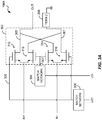
- FIG. 3A is a diagram of a single-ended mixer according to one embodiment.
- the illustrated mixer 108A receives a differential input signal, IN + and IN-, and a differential local oscillator signal, LO + and LO -, and generates a single-ended output, OUT.
- the illustrated mixer 108A includes a mixer core 302, a matching network 304 coupled to a LO negative differential node 307 of the mixer core 302 and a matching network 306 coupled to a LO positive differential node 305 of the mixer core 302.
- the mixer core 302 includes a first differential node 301 and a second differential node 303.
- the first differential node 301 of the mixer core 302 is coupled to a termination impedance 308, and the second differential node 303 of the mixer core 302 provides the single-ended output, OUT.
- the illustrated mixer 108A in FIGS. 3A-3B can be implemented in a receive circuit and/or a transmit circuit for mixing functions, such as down converting or up converting.
- the differential input signal, IN + and IN - may correspond to a differential RF signal in a receive circuit or a differential IF signal in a transmit circuit.
- the single-ended output signal, OUT may correspond to an IF signal in a receive circuit or a RF signal in a transmit circuit.
- the mixer core 302 includes transistors 310, 312, 314, and 316 configured to mix the differential input and differential local oscillator signals to generate a differential mixer core output across the first differential node 301 and the second differential node 303.
- the mixer core 302 can be a passive quad FET mixer or a FET ring mixer, which can be implemented with NFET and/or PFET transistors.
- each transistor can operate as a switch that is either on or off.
- the transistors for a passive mixer can electrically connect two nodes when on and electrically isolate the two nodes when off.
- transistors can be periodically turned on and off to mix signals.
- a passive mixer can be in series with an active circuit and pass DC current of the active circuit.
- the differential LO signal, LO + and LO -, received at the differential LO nodes 305, 307 by way of the matching networks 304, 306, can turn different transistors 310, 312, 314, and 316 of the mixer core 302 on and off.
- the mixer core 302 can alternatingly connect the differential input, IN + and IN -, at the differential input nodes to the differential output nodes of the mixer core 302.
- one of the differential output nodes 301, 303 of the mixer core 302 is terminated with the termination impedance 308 while the other differential output node of the mixer core 302 produces the single-ended output, OUT, of the mixer 108A.
- the differential node 301 is coupled to the termination impedance 308 while the differential node 303 provides the single-ended output, OUT, but the selection of a termination node and a mixer output node can vary in other embodiments.
- the termination impedance 308 can be implemented with a resistor.
- the termination impedance 308 can be implemented with other passive circuit elements such as one or more capacitors and/or inductors implementing complex impedance.
- a combination of a resistor and one or more other passive impedance elements can implement the termination impedance 308 according to certain embodiments.
- the termination impedance 308 can be implemented to have a mismatched termination impedance that is at least one order of magnitude higher than the overall circuit's standard operational or design environment.
- some or all of the elements of the circuits illustrated in FIGS. 1A-5 herein may be designed in a standard environment, such as a 50 Ohm environment for RF circuits.
- the termination impedance 308 can have an impedance that is sufficiently high at a frequency within a range of interest (e.g., one or more ranges of radio frequency) such that the mixer 108A has a reduction in gain of no more than about 1 dB resulting from the termination impedance 308.
- a range of interest e.g., one or more ranges of radio frequency
- the termination impedance 308 disclosed herein can be, for example, in a range from about 500 ⁇ to 5,000 ⁇ at a radio frequency, instead of being about 50 ⁇ that matches the standard impedance.
- the impedance of the termination impedance can in a range from about 1 k ⁇ to 2 k ⁇ at a radio frequency.
- the termination impedance 308 can be implemented by a 2 k ⁇ termination resistor.
- a resistor of a fixed mismatched impedance e.g., 1 k ⁇ in an RF circuit
- additional circuit elements can be used to implement a complex impedance that is about at least one order of magnitude higher than the standard impedance (e.g., 50 ⁇ in an RF circuit) at a frequency within a range of interest (e.g., one or more ranges of radio frequency).
- the negative and positive differential oscillator signal nodes 305, 307 of the mixer core 302 can be coupled to the matching networks 304 and 306, respectively.
- the matching networks 304, 306 can be implemented to counter the effects of the mismatched termination at the singled-ended output implemented with the termination impedance 308 or otherwise further improve functionality of the mixer 108A.
- the matching networks 304, 306 can be implemented, for example, with passive circuit elements such as resistors, capacitors, inductors, or any suitable combination thereof.
- the matching network 304 can be implemented to have different values and/or characteristics than the matching network 306.
- These matching networks can be mismatched to counterbalance and/or compensate for the mismatch on the outputs of the mixer core 302 resulting from the relatively high impedance termination impedance 308.
- the mismatch of the matching networks 304, 306 can be implemented to counterbalance the mismatch on output nodes of the mixer core 302 and provide sufficient leakage and isolation performance in the mixer.
- mismatching termination impedance can result in degradation in insolation due to compromised signal differentiality of the differential signals at the nodes 301, 303 of the mixer core 302, which can allow output leakage.
- the matching networks 304, 306 can be implemented to reduce the degradation in isolation by countering the mismatch at the nodes 301, 303 of the mixer core 302 to restore signal differentiality and reduce leakage.
- the matching networks 304, 306 can be implemented with various passive circuit components, such as one or more of resistors, capacitors, inductors, etc. An example implementation of the matching networks 304, 306 is discussed in connection with FIG. 4E below.
- matching networks 304, 306 can be implemented at the local oscillator side (e.g., at nodes 305, 307) as shown in FIGS. 3A , 3B , 4A , 4B below.
- matching networks 309, 311 can be implemented at the input signal side (e.g., at nodes 317, 319) as shown in FIGS. 3C , 3D , 4C , 4D below.
- matching networks can be implemented at both the local oscillator side and at the input signal side according to certain embodiments.
- one or more matching networks can be implemented at one or more of the nodes of the local oscillator and/or input signal side of the mixer core 302. It is to be noted that various different matching topologies can be used to implement one or more of the matching networks 304, 306, 309, 311, and the topology of the matching networks and the values of the components of the matching networks can be selected based on circuit design principles according to the frequency of operation and an acceptable level of leakage.
- a single-ended mixer implemented as disclosed herein can be advantageous in reducing loss in gain resulting from a standard or nominal impedance commonly used in circuit designs. For instance, using the standard 50 ⁇ termination resistor for a single-ended RF mixer can result in a 3 dB loss in gain. By using a mismatched high impedance for termination of a single-ended mixer as disclosed herein, the 3 dB insertion loss can be reduced. For instance, a 24-27 GHz FET mixer implemented using the technology disclosed herein can achieve a low average conversion loss of about 8 dB rather than an average conversion loss of about 10 dB while achieving a high typical third-order input intercept point (IIP3) of about 25 dBm.
- IIP3 third-order input intercept point
- the mixers disclosed herein can be accompanied with LO nulling to improve the LO-RF isolation.
- an LO nulling can be implemented by applying a relatively small DC offset typically in the order of about 10 mV to 30 mV at the mixer outputs.
- the DC offset can improve the LO-RF isolation reaching relatively high levels, up to 80 dB in certain implementations.
- the LO nulling technique can be employed when the frequency range of interest is relatively narrow and relatively high levels of isolation are desired in the relatively narrow frequency range. Further details of the improved performance of a single-ended mixer implemented as disclosed herein are illustrated and described in connection with FIGS. 6-8 below.
- FIG. 3B is a diagram of a single-ended mixer according to another embodiment.
- the mixer 108A illustrated in FIG. 3B includes similar circuit elements corresponding to the elements of the mixer illustrated in FIG. 3A , except that the mixer illustrated in FIG. 3B includes a resistor 318 implementing the termination impedance 308 ( FIG. 3A ).
- the termination resistor 318 should have the same impedance for all frequencies. Accordingly, the mixer 108A of FIG. 3B can be used for mixing a variety signals having different frequencies without the termination impedance changing.
- the resistance of the resistor 318 can have any suitable characteristics of the termination impedance 308 discussed above.
- the resistance of the termination resistor 318 can be at least one order of magnitude higher than a standard termination resistance or matching impedance, such as 50 ⁇ .
- the resistance of the termination resistor 318 can be in a range from about 500 ⁇ to 5,000 ⁇ .
- the disclosed technology can be implemented with the resistor 318 of about 2 k ⁇ in an RF circuit.
- the resistance of the termination resistor 318 can be sufficiently high such that the mixer 108A has a reduction in gain of no more than a desired amount (e.g., about 1 dB) resulting from the impedance of the termination resistor 318.
- certain design considerations, such as parasitic effects can be additionally considered in selecting a suitable resistance of the termination resistor 318.
- FIG. 3C is a diagram of a single-ended mixer according to another embodiment.
- the mixer 108A illustrated in FIG. 3C includes similar circuit elements corresponding to the elements of the mixer illustrated in FIG. 3A , except that the mixer illustrated in FIG. 3C includes a matching network 309 coupled to an IN positive differential node 317 of the mixer core 302 and a matching network 311 coupled to an IN negative differential node 319 of the mixer core 302.
- the matching networks 309, 311 can be implemented in accordance with any of the principles and advantages discussed with reference to FIG. 3A .
- FIG. 3D is a diagram of a single-ended mixer according to another embodiment.
- the mixer 108A illustrated in FIG. 3D includes similar circuit elements corresponding to the elements of the mixer illustrated in FIG. 3C , except that the mixer illustrated in FIG. 3B includes a resistor 318 implementing the termination impedance 308 ( FIG. 3C ).
- the resistor 318 can be implemented in accordance with any of the principles and advantages discussed with reference to FIG. 3B .
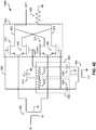
- FIG. 4A is a diagram of a single-ended mixer according to another embodiment.
- the illustrated mixer 108B is a double-balanced FET ring mixer or a double-balanced quad FET mixer.
- the illustrated mixer 108B receives an input signal, IN, and a local oscillator signal, LO, and generates a single-ended output, OUT.
- the input signal, IN, and the local oscillator signal, LO are both single-ended signals in the mixer 108B.
- the illustrated mixer 108B includes an input balun 402, a local oscillator balun 404, the mixer core 302, the matching networks 304, 306, and a termination impedance 308.
- the input balun 402 can receive the single-ended input signal, IN, and provide a differential input signal to the mixer core 302.
- the local oscillator balun 404 can receive the single-ended local oscillator signal, LO, and provide a differential local oscillator signal to the mixer core 302.
- either or both of the baluns 402, 404 can be mismatched to counterbalance the mismatch at the output nodes 301, 303 of the mixer core 302 in addition to or instead of one or more of the matching networks 304, 306, 309, 311.
- mismatching of either or both of the baluns 402, 404 can be implemented by changing the number of turns of balun differential outputs.
- the illustrated mixer 108B in FIG. 4A can be implemented in a receive circuit and/or a transmit circuit for mixing functions, such as down converting or up converting.
- the input signal, IN may correspond to a RF signal in a receive circuit or an IF signal in a transmit circuit.
- the single-ended output signal may correspond to an IF signal in a receive circuit or a RF signal in a transmit circuit.
- one of the differential outputs of the mixer core 302 is terminated with the termination impedance 308 while the other differential output of the mixer core 302 produces the single-ended output, OUT, of the mixer 108B.
- the mixer illustrated in FIG. 4A includes similar elements corresponding to the elements of the mixer illustrated in FIG. 3A and has similar characteristics and can achieve similar advantages.
- FIG. 4B is a diagram of a single-ended mixer according to another embodiment.
- the mixer 108B illustrated in FIG. 4B includes similar circuit elements corresponding to the elements of the mixer illustrated in FIG. 4A , except that the mixer illustrated in FIG. 4B includes the resistor 318 implementing the termination impedance 308 ( FIG. 4A ).
- the resistor 318 can be implemented in accordance with any of the principles and advantages discussed with reference to FIG. 3B .
- the resistance of the resistor 318 can have any of the resistance values discussed with reference to FIG. 3B .
- FIG. 4C is a diagram of a single-ended mixer according to another embodiment.
- the mixer 108B illustrated in FIG. 4C includes similar circuit elements corresponding to the elements of the mixer illustrated in FIG. 4A , except that the mixer illustrated in FIG. 4C includes the matching networks 309, 311 coupled to the differential nodes 317, 319 of the mixer core 302, respectively.
- the matching networks 309, 311 can be implemented in accordance with any of the principles and advantages discussed with reference to FIG. 3C .
- FIG. 4D is a diagram of a single-ended mixer according to another embodiment.
- the mixer 108B illustrated in FIG. 4D includes similar circuit elements corresponding to the elements of the mixer illustrated in FIG. 4C , except that the mixer illustrated in FIG. 4D includes the resistor 318 implementing the termination impedance 308 ( FIG. 4C ).
- the resistor 318 can be implemented in accordance with any of the principles and advantages discussed with reference to FIG. 3B .
- FIG. 4E is a diagram of a single-ended mixer according to another embodiment.
- the mixer 108B illustrated in FIG. 4E includes similar circuit elements corresponding to the elements of the mixer illustrated in FIG. 4B , except that the mixer illustrated in FIG. 4E provides illustrative matching networks 304 and 306.
- a resistor 410 and a capacitor 406 implement the matching network 306 and a resistor 412 and a capacitor 408 implement the matching network 304.
- a DC bias source 414 provides a DC bias voltage to the matching networks 304 and 306.
- the resistors 410, 412 and the capacitors 406, 408 can be implemented in accordance with any of the principles and advantages of the matching networks 304, 306 discussed with reference to FIG.
- the resistance of the resistor 410 can be in a range from about 0.5 k ⁇ to 5 k ⁇ , such as about 1 k ⁇ .
- the capacitance of the capacitor 406 can be in a range from about 0.5 pF to about 5 pF, such as about 2 pF.
- the resistance of the resistor 412 can be have a similar resistance to the resistor 410, and the capacitance of the capacitor 408 can be similar to the capacitor 406.
- the resistance of the resistors 410 and 412 and the capacitance of the capacitors 406, 408 can be selected based on various considerations.
- the resistance of the resistors 410 and 412 can be selected according to considerations, such as coupling of the LO signal and the bias line connected to the DC bias source 414 and the impedance seen from the gates of the transistors 310, 312, 314, 316. For example, a resistance of 1 k ⁇ or higher can be beneficial for reducing couple of the LO signal and the bias line, if any, and making the impedance seen from the gates to be relatively small.
- the capacitors 406, 408 can be part of the matching network 306, 304 that can be multi-section matching, which is suitable for wideband applications. The capacitance of the capacitors 406, 408 can be selected based on the mixer operating frequency range.
- the resistance and/or capacitance of the matching networks 304, 306 can be of different values, respectively, for improved LO isolation.
- the DC biasing can be implemented with an external pin that is provided to the mixer chip and connected to the DC bias source 414.
- the DC bias level can be the pinch-off voltage of the transistors of the mixer 108, such as FETs..
- any suitable principles and advantages described herein can be implemented in mixers with one of the input signal IN and the local oscillator signal LO as a differential signal while the other is single-ended signal.
- one of the baluns 402, 404 can be omitted.
- all or any combination of the matching networks 304, 306, 309, and 311 can be used to implement different matching topologies to counter the mismatched termination impedance as appropriate.
- FIG. 5 is a diagram of an example layout of circuit elements according to one embodiment.
- the illustrated layout 500 of FIG. 5 includes the termination impedance 308, the mixer core 302 having field effect transistors 502, 504, 506, and 508, and a high impedance connection 510. It is to be noted that layouts of electric connections between the illustrated circuit elements (e.g., the termination impedance 308, the FETs 502, 504, 506, and 508) are omitted in FIG. 5 . Although not expressly illustrated in FIG.
- the termination impedance 308 is coupled to one of the differential output nodes of the mixer core 302 as discussed above, and the high impedance connection 510 is coupled to the other of the differential output nodes of the mixer core 302 to produce the single-ended output, OUT, of the mixers 108A, 108B in FIGS. 3A-4B .
- the termination impedance 308 can be implemented with a resistor having a mismatched high magnitude resistance in the range from about 500 ⁇ to 5,000 ⁇ in an RF circuit, for example.
- the sizes of the individual elements (e.g., 308, 502, 504, 506, and 508) of the layout 500 are not necessarily to scale and the solid lines do not necessarily illustrate the actual shapes, dimensions, or aspect ratios of these elements.
- the elements 308, 502, 504, 506, and 508 of the physical layout 500 are depicted to illustrate the relative distances between one another according to one embodiment.
- the disclosed herein can be implemented with a distance between the FET 502 and the FET 504 being in the range of about 30 ⁇ m to 100 ⁇ m and a distance between the terminal impedance 308 and the FET 502 or between the termination impedance 308 and the FET 504 being in the range of also about 30 ⁇ m to 100 ⁇ m.
- the distance between the terminal impedance 308 and one of the FETs 502, 504, 506, and 508 that is the closest to the terminal impedance 308 can be considered comparable to the distance between two of the FETs 502, 504, 506, and 508 that are adjacent to each other.
- the "comparable" distance can be understood as the distance that is a distance of the same or similar magnitude as the distance to which it is comparable.
- the FETs 502, 504, 506, and 508 can be formed adjacent to one another at an operational distance, and the FETs 502, 504, 506, and 508 are arranged as the mixer core 302.
- the high termination impedance 308 can be formed adjacent to one of the FETs 502, 504, 506, and 508 at a distance comparable to the operational distance of the FETs 502, 504, 506, and 508 within the mixer core 302.
- the "distance" between the elements (308, 502, 504, 506, and 508) of the layout 500 can be understood as the shortest straight line distance between a point on the outermost outline of one element and a point on the outermost outline of another element.
- the FETs 502, 504, 506, and 508 of the mixer core 302 can be physically located as closest as possible, or be near or at minimum operational distance to one another to reduce size.
- the termination impedance 308 can be designed to be as closest to one or more FETs (502, 504, 506, and 508) of the mixer core 302 as possible, or be at or near minimum operational distance to the one or more FETs 502, 504, 506, and 508.
- the "operational" distance can be understood as the distance allowing the intended individual functionalities of the elements (308, 502, 504, 506, and 508) without significant interference or degradation in performance resulting from a close physical proximity of the elements (308, 502, 504, 506, and 508).
- Such an operational distance can be defined by layout rules for a particular process technology.
- the one or more distances between the termination impedance 308, the FETs 502, 504, 506, and 508, and the mixer core 302 can further be adjusted according to the trade-offs between performance, size, and design restrictions (e.g., right-angled or 45° connections rather than straight Euclidian line connections).
- a single-ended mixer as disclosed herein with suitable distances between the elements can be advantageous in allowing a broader bandwidth of operation.
- having the termination impedance 308 as close as possible and/or with the shortest connection to the mixer core 302 e.g., to one or more of the FETs 502, 504, 506, and 508) can increase bandwidth of the single-ended mixer.
- the physical layout and/or the physical arrangement of the elements e.g., 308, 502, 504, 506, and 508) can be selected to allow acceptable bandwidth for the mixer operation with the benefit of a reduced loss in gain discussed above in connection with FIG. 3A .
- the mixers 108A, 108B can provide a broad range of connections.
- the illustrated arrangement of the elements (308, 502, 504, 506, and 508) in FIG. 5 e.g., the termination impedance 308 being on the left side of the mixer core 302 and being vertically about half way over the vertical dimension of the mixer core 302 and the FETs 502, 504, 506, and 508 being in a 2 by 2 arrangement forming the mixer core 302, show only one example arrangement of the elements (308, 502, 504, 506, and 508).
- the FETs 502, 504, 506, and 508 and the termination impedance 308 can be arranged differently with the termination impedance 308 and one or more of the FETs 502, 504, 506, and 508 being at comparable and/or approximately minimum operational distances from one another.
- FIG. 5 also includes the high impedance connection 510 depicted in dotted lines.
- the high impedance connection 510 does not necessarily illustrate an actual layout of a high impedance line and is included to represent the connection from one of the differential output nodes of the mixer core 302 to the single-ended output node of the mixers 108A ( FIGS. 3A-3B ), 108B ( FIGS. 4A-4B ), which can include a pad that can be coupled to a circuit element external to the mixer.
- the high impedance connection 510 for example, can be implemented with a conductive line with a selection of different materials and/or lengths to achieve the desired impedance.
- the high impedance connection 510 can be implemented in connection with a single-ended output of any of the mixers discussed herein.
- the illustrated termination impedance 308 and the FETs 502, 504, 506, and 508 of the mixer core 302 can be on one die.
- one or more elements illustrated in FIGS. 1A-4B can be implemented on a single die.
- the LO e.g., 110 in FIGS. 1A-2B
- the LO can be in the same package as one or more of the mixers 108A, 108B, and in other embodiments, the LO can be in a different package.
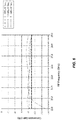
- FIG. 6 is a simulation graph of an example single-ended mixer implemented according to the embodiments disclosed herein.
- the graph in FIG. 6 shows conversion gain over a range of RF frequency (from 22 GHz to 29 GHz) in three different cases of IF frequency (0 GHz, 2.5 GHz, and 5 GHz) for an example implementation of the technology disclosed herein.
- the example implementation here is an I/Q mixer having an operating range of 24-27 GHz and with RF and LO baluns designed in a 50 Ohm environment.
- a Lange coupler was used to provide a phase difference of 90 degrees between the I and Q channels, and a low-loss lumped Wilkinson combiner was used to combine the RF outputs.
- this example I/Q mixer can achieve an average conversion gain of about -8 dB (or loss of 8 dB) with a minimum conversion loss of about 9 dB.
- FIG. 7 is another simulation graph of the single-ended mixer discussed in connection with FIG. 6 .
- the graph in FIG. 7 shows third-order input intercept point (IIP3) over a range of RF frequency (from 22 GHz to 29 GHz) in three different cases of IF frequency (0 GHz, 2.5 GHz, and 5 GHz).
- IIP3 third-order input intercept point
- this example I/Q mixer can achieve IIP3 of about 25 dBm with a minimum IIP3 of about 22 dBm.
- FIG. 8 is another simulation graph of the single-ended mixer discussed in connection with FIG. 6 .
- the graph in FIG. 8 shows LO-RF isolation over a range of RF frequency (from 22 GHz to 29 GHz) before and after the LO nulling technique is used.
- this example I/Q mixer implemented without the LO nulling can achieve the minimum LO-RF isolation of about 25 dB, while the LO nulling can improve the minimum LO-RF isolation of the example I/Q mixer to about 65 dBm.
- aspects of this disclosure can be implemented in various electronic devices. For instance, aspects of this disclosure can be implemented in any electronic device or electronic component that could benefit from a single-ended mixer. As an example, aspects of this disclosure can be implemented in any electronic device or electronic component with a transmitter, receiver, or transceiver that could benefit from a single-ended mixer. Examples of the electronic devices can include, but are not limited to, consumer electronic products, parts of the consumer electronic products, electronic test equipment, vehicular electronics systems, etc. Examples of the electronic devices can include, but are not limited to, computing devices, communications devices, electronic household appliances, automotive electronics systems, etc. Further, the electronic devices can include unfinished products.
- conditional language used herein such as, among others, “can,” “could,” “might,” “may,” “e.g.,” “for example,” “such as” and the like, unless specifically stated otherwise, or otherwise understood within the context as used, is generally intended to convey that certain embodiments include, while other embodiments do not include, certain features, elements and/or states.
- conditional language is not generally intended to imply that features, elements and/or states are in any way required for one or more embodiments or that one or more embodiments necessarily include logic for deciding, with or without author input or prompting, whether these features, elements and/or states are included or are to be performed in any particular embodiment.
- any suitable means capable of performing the operations such as various hardware and/or software component(s), circuits, and/or module(s).
- any operations illustrated in the Figures may be performed by corresponding functional means capable of performing the operations.
Landscapes
- Engineering & Computer Science (AREA)
- Power Engineering (AREA)
- Transceivers (AREA)
- Amplifiers (AREA)
- Superheterodyne Receivers (AREA)
Applications Claiming Priority (1)
| Application Number | Priority Date | Filing Date | Title |
|---|---|---|---|
| US15/008,183 US9602055B1 (en) | 2016-01-27 | 2016-01-27 | Single-ended mixer with reduced loss |
Publications (2)
| Publication Number | Publication Date |
|---|---|
| EP3200342A1 true EP3200342A1 (de) | 2017-08-02 |
| EP3200342B1 EP3200342B1 (de) | 2020-02-26 |
Family
ID=57914737
Family Applications (1)
| Application Number | Title | Priority Date | Filing Date |
|---|---|---|---|
| EP17152846.6A Active EP3200342B1 (de) | 2016-01-27 | 2017-01-24 | Asymmetrischer mischer mit verringertem verlust |
Country Status (3)
| Country | Link |
|---|---|
| US (1) | US9602055B1 (de) |
| EP (1) | EP3200342B1 (de) |
| CN (1) | CN107017847B (de) |
Families Citing this family (7)
| Publication number | Priority date | Publication date | Assignee | Title |
|---|---|---|---|---|
| US9929760B2 (en) * | 2016-04-14 | 2018-03-27 | Taiwan Semiconductor Manufacturing Co., Ltd. | Ultra-low-power RF receiver frontend with tunable matching networks |
| US10523156B2 (en) * | 2017-06-29 | 2019-12-31 | Hrl Laboratories, Llc | Mixer with series connected active devices |
| US10523254B2 (en) | 2017-07-20 | 2019-12-31 | Qualcomm Incorporated | Mixer S11 control via sum component termination |
| CN110945781B (zh) * | 2017-07-20 | 2022-12-27 | 华为技术有限公司 | 具有对称边带增益的单平衡电压模式无源混频器 |
| CN108551331A (zh) * | 2018-03-23 | 2018-09-18 | 杭州电子科技大学 | 一种基于变压器耦合匹配的毫米波低损耗倍频器 |
| CN109525199A (zh) * | 2018-11-19 | 2019-03-26 | 中电科仪器仪表有限公司 | 基于多层基材微带电路结构的无源、双平衡i/q混频器 |
| CN113965169B (zh) * | 2021-12-22 | 2022-03-18 | 中国移动通信有限公司研究院 | 变频方法、装置及系统 |
Citations (6)
| Publication number | Priority date | Publication date | Assignee | Title |
|---|---|---|---|---|
| EP0336191A1 (de) * | 1988-04-05 | 1989-10-11 | Nokia Mobile Phones Ltd. | Schaltung, um einen differentialen Ausgang in einen unsymmetrischen Ausgang umzuwandeln |
| EP0498221A1 (de) * | 1991-01-24 | 1992-08-12 | Nec Corporation | Schaltung zur Frequenzverdopplung und zur Mischung |
| US5361409A (en) * | 1991-03-12 | 1994-11-01 | Watkins Johnson Company | FET mixer having transmission line transformer |
| US5732345A (en) * | 1995-12-20 | 1998-03-24 | Watkins-Johnson Company | Quasi-double balanced dual-transformer dual FET mixer, which achieves better isolation by using a first and second diplexer, and a transmission line RF balun |
| US6150852A (en) * | 1999-01-14 | 2000-11-21 | Qualcomm Incorporated | Active differential to single-ended converter |
| US20140097882A1 (en) * | 2012-10-08 | 2014-04-10 | Marki Microwave, Inc. | Mixer fabrication technique and system using the same |
Family Cites Families (6)
| Publication number | Priority date | Publication date | Assignee | Title |
|---|---|---|---|---|
| US5086512A (en) | 1988-04-20 | 1992-02-04 | Hewlett-Packard Company | Compensation system for dynamically tracking and nulling local oscillator feedthrough |
| US5774801A (en) | 1995-08-23 | 1998-06-30 | Ericsson Inc. | High dynamic range mixer having low conversion loss, low local oscillator input power, and high dynamic range and a method for designing the same |
| US6713938B2 (en) | 1999-01-14 | 2004-03-30 | The Regents Of The University Of Michigan | Method and apparatus for filtering signals utilizing a vibrating micromechanical resonator |
| US20080014873A1 (en) | 2006-07-12 | 2008-01-17 | Krayer Yvonne L | Methods and apparatus for adaptive local oscillator nulling |
| CN103051288B (zh) * | 2012-12-14 | 2015-05-06 | 东南大学 | 一种可重构无源混频器 |
| US9692473B2 (en) * | 2014-05-16 | 2017-06-27 | Analog Devices, Inc. | Offset compensation in a receiver |
-
2016
- 2016-01-27 US US15/008,183 patent/US9602055B1/en active Active
-
2017
- 2017-01-24 EP EP17152846.6A patent/EP3200342B1/de active Active
- 2017-01-25 CN CN201710055345.0A patent/CN107017847B/zh active Active
Patent Citations (6)
| Publication number | Priority date | Publication date | Assignee | Title |
|---|---|---|---|---|
| EP0336191A1 (de) * | 1988-04-05 | 1989-10-11 | Nokia Mobile Phones Ltd. | Schaltung, um einen differentialen Ausgang in einen unsymmetrischen Ausgang umzuwandeln |
| EP0498221A1 (de) * | 1991-01-24 | 1992-08-12 | Nec Corporation | Schaltung zur Frequenzverdopplung und zur Mischung |
| US5361409A (en) * | 1991-03-12 | 1994-11-01 | Watkins Johnson Company | FET mixer having transmission line transformer |
| US5732345A (en) * | 1995-12-20 | 1998-03-24 | Watkins-Johnson Company | Quasi-double balanced dual-transformer dual FET mixer, which achieves better isolation by using a first and second diplexer, and a transmission line RF balun |
| US6150852A (en) * | 1999-01-14 | 2000-11-21 | Qualcomm Incorporated | Active differential to single-ended converter |
| US20140097882A1 (en) * | 2012-10-08 | 2014-04-10 | Marki Microwave, Inc. | Mixer fabrication technique and system using the same |
Also Published As
| Publication number | Publication date |
|---|---|
| EP3200342B1 (de) | 2020-02-26 |
| CN107017847A (zh) | 2017-08-04 |
| CN107017847B (zh) | 2020-12-01 |
| US9602055B1 (en) | 2017-03-21 |
Similar Documents
| Publication | Publication Date | Title |
|---|---|---|
| EP3200342B1 (de) | Asymmetrischer mischer mit verringertem verlust | |
| JP7324233B2 (ja) | ミリ波5g通信用再構成可能バンド幅を用いたワイドバンド低雑音増幅器(lna) | |
| US11290064B2 (en) | Amplifier | |
| US8571511B2 (en) | Apparatus and method for a wideband RF mixer | |
| KR102557851B1 (ko) | 멀티-대역 밀리미터파 5g 통신을 위한 송신 및 수신 스위치 및 브로드밴드 전력 증폭기 매칭 네트워크 | |
| US10826457B2 (en) | Broadband power amplifier and matching network for multi-band millimeter-wave 5G communication | |
| EP3429076B1 (de) | Mischer mit verbesserter linearität | |
| JP7202398B2 (ja) | ミリ波5g通信用ブロードバンドmimo受信機のための送信/受信(t/r)スイッチ及び受信機フロントエンドのワイドバンドマッチング共設計法 | |
| CN114514704A (zh) | 用于毫米波无线通信的宽带发射器 | |
| CN103684289A (zh) | 推挽式放大器和差动推挽式放大器 | |
| Deng et al. | Tunable quasi-circulator based on a compact fully-reconfigurable 180° hybrid for full-duplex transceivers | |
| WO2016034740A1 (en) | Iq signal generator system and method | |
| US11025201B2 (en) | Power efficient radio mixers | |
| KR20230106176A (ko) | 다중 대역 밀리미터-파 5g 통신에서 소형 이미지 제거 아키텍처를 위한 임베디드 iq 발생을 이용한 변압기 기반 전류 재사용 증폭기 | |
| Lee et al. | A 150-GHz Single-to-Differential LNA Adopting Wideband G max-Cores Based on Single-Ended Compact Lumped L-C-L and Differential Coupled-Line Embedding Networks | |
| Aneja et al. | Design of continuously tunable low noise amplifier for multiband radio | |
| Yeh et al. | Review of millimeter-wave MMIC mixers | |
| Gharaba et al. | A 2mW, 60GHz Mixer First I/Q Receiver in 28nm CMOS | |
| US20240364264A1 (en) | Input matching network with harmonic trap for frequency multiplier | |
| Yu et al. | High-Linearity Double-Balanced Up-Conversion Mixer with an Active Balun Based on InGaP/GaAs HBT Technique | |
| Chen et al. | A Ku-Band Two-stage Cascode Power Amplifier for Satellite Application in 180-nm CMOS Technology | |
| JPWO2012111848A1 (ja) | ミキサ回路 |
Legal Events
| Date | Code | Title | Description |
|---|---|---|---|
| PUAI | Public reference made under article 153(3) epc to a published international application that has entered the european phase |
Free format text: ORIGINAL CODE: 0009012 |
|
| STAA | Information on the status of an ep patent application or granted ep patent |
Free format text: STATUS: THE APPLICATION HAS BEEN PUBLISHED |
|
| AK | Designated contracting states |
Kind code of ref document: A1 Designated state(s): AL AT BE BG CH CY CZ DE DK EE ES FI FR GB GR HR HU IE IS IT LI LT LU LV MC MK MT NL NO PL PT RO RS SE SI SK SM TR |
|
| AX | Request for extension of the european patent |
Extension state: BA ME |
|
| STAA | Information on the status of an ep patent application or granted ep patent |
Free format text: STATUS: REQUEST FOR EXAMINATION WAS MADE |
|
| 17P | Request for examination filed |
Effective date: 20180130 |
|
| RBV | Designated contracting states (corrected) |
Designated state(s): AL AT BE BG CH CY CZ DE DK EE ES FI FR GB GR HR HU IE IS IT LI LT LU LV MC MK MT NL NO PL PT RO RS SE SI SK SM TR |
|
| RAP1 | Party data changed (applicant data changed or rights of an application transferred) |
Owner name: ANALOG DEVICES GLOBAL UNLIMITED COMPANY |
|
| GRAP | Despatch of communication of intention to grant a patent |
Free format text: ORIGINAL CODE: EPIDOSNIGR1 |
|
| STAA | Information on the status of an ep patent application or granted ep patent |
Free format text: STATUS: GRANT OF PATENT IS INTENDED |
|
| INTG | Intention to grant announced |
Effective date: 20190823 |
|
| GRAS | Grant fee paid |
Free format text: ORIGINAL CODE: EPIDOSNIGR3 |
|
| GRAA | (expected) grant |
Free format text: ORIGINAL CODE: 0009210 |
|
| STAA | Information on the status of an ep patent application or granted ep patent |
Free format text: STATUS: THE PATENT HAS BEEN GRANTED |
|
| AK | Designated contracting states |
Kind code of ref document: B1 Designated state(s): AL AT BE BG CH CY CZ DE DK EE ES FI FR GB GR HR HU IE IS IT LI LT LU LV MC MK MT NL NO PL PT RO RS SE SI SK SM TR |
|
| REG | Reference to a national code |
Ref country code: GB Ref legal event code: FG4D |
|
| REG | Reference to a national code |
Ref country code: CH Ref legal event code: EP |
|
| REG | Reference to a national code |
Ref country code: AT Ref legal event code: REF Ref document number: 1238882 Country of ref document: AT Kind code of ref document: T Effective date: 20200315 |
|
| REG | Reference to a national code |
Ref country code: IE Ref legal event code: FG4D |
|
| REG | Reference to a national code |
Ref country code: DE Ref legal event code: R096 Ref document number: 602017012102 Country of ref document: DE |
|
| PG25 | Lapsed in a contracting state [announced via postgrant information from national office to epo] |
Ref country code: RS Free format text: LAPSE BECAUSE OF FAILURE TO SUBMIT A TRANSLATION OF THE DESCRIPTION OR TO PAY THE FEE WITHIN THE PRESCRIBED TIME-LIMIT Effective date: 20200226 Ref country code: NO Free format text: LAPSE BECAUSE OF FAILURE TO SUBMIT A TRANSLATION OF THE DESCRIPTION OR TO PAY THE FEE WITHIN THE PRESCRIBED TIME-LIMIT Effective date: 20200526 Ref country code: FI Free format text: LAPSE BECAUSE OF FAILURE TO SUBMIT A TRANSLATION OF THE DESCRIPTION OR TO PAY THE FEE WITHIN THE PRESCRIBED TIME-LIMIT Effective date: 20200226 |
|
| REG | Reference to a national code |
Ref country code: NL Ref legal event code: MP Effective date: 20200226 |
|
| REG | Reference to a national code |
Ref country code: LT Ref legal event code: MG4D |
|
| PG25 | Lapsed in a contracting state [announced via postgrant information from national office to epo] |
Ref country code: SE Free format text: LAPSE BECAUSE OF FAILURE TO SUBMIT A TRANSLATION OF THE DESCRIPTION OR TO PAY THE FEE WITHIN THE PRESCRIBED TIME-LIMIT Effective date: 20200226 Ref country code: LV Free format text: LAPSE BECAUSE OF FAILURE TO SUBMIT A TRANSLATION OF THE DESCRIPTION OR TO PAY THE FEE WITHIN THE PRESCRIBED TIME-LIMIT Effective date: 20200226 Ref country code: IS Free format text: LAPSE BECAUSE OF FAILURE TO SUBMIT A TRANSLATION OF THE DESCRIPTION OR TO PAY THE FEE WITHIN THE PRESCRIBED TIME-LIMIT Effective date: 20200626 Ref country code: HR Free format text: LAPSE BECAUSE OF FAILURE TO SUBMIT A TRANSLATION OF THE DESCRIPTION OR TO PAY THE FEE WITHIN THE PRESCRIBED TIME-LIMIT Effective date: 20200226 Ref country code: BG Free format text: LAPSE BECAUSE OF FAILURE TO SUBMIT A TRANSLATION OF THE DESCRIPTION OR TO PAY THE FEE WITHIN THE PRESCRIBED TIME-LIMIT Effective date: 20200526 Ref country code: GR Free format text: LAPSE BECAUSE OF FAILURE TO SUBMIT A TRANSLATION OF THE DESCRIPTION OR TO PAY THE FEE WITHIN THE PRESCRIBED TIME-LIMIT Effective date: 20200527 |
|
| PG25 | Lapsed in a contracting state [announced via postgrant information from national office to epo] |
Ref country code: NL Free format text: LAPSE BECAUSE OF FAILURE TO SUBMIT A TRANSLATION OF THE DESCRIPTION OR TO PAY THE FEE WITHIN THE PRESCRIBED TIME-LIMIT Effective date: 20200226 |
|
| PG25 | Lapsed in a contracting state [announced via postgrant information from national office to epo] |
Ref country code: DK Free format text: LAPSE BECAUSE OF FAILURE TO SUBMIT A TRANSLATION OF THE DESCRIPTION OR TO PAY THE FEE WITHIN THE PRESCRIBED TIME-LIMIT Effective date: 20200226 Ref country code: SM Free format text: LAPSE BECAUSE OF FAILURE TO SUBMIT A TRANSLATION OF THE DESCRIPTION OR TO PAY THE FEE WITHIN THE PRESCRIBED TIME-LIMIT Effective date: 20200226 Ref country code: EE Free format text: LAPSE BECAUSE OF FAILURE TO SUBMIT A TRANSLATION OF THE DESCRIPTION OR TO PAY THE FEE WITHIN THE PRESCRIBED TIME-LIMIT Effective date: 20200226 Ref country code: RO Free format text: LAPSE BECAUSE OF FAILURE TO SUBMIT A TRANSLATION OF THE DESCRIPTION OR TO PAY THE FEE WITHIN THE PRESCRIBED TIME-LIMIT Effective date: 20200226 Ref country code: SK Free format text: LAPSE BECAUSE OF FAILURE TO SUBMIT A TRANSLATION OF THE DESCRIPTION OR TO PAY THE FEE WITHIN THE PRESCRIBED TIME-LIMIT Effective date: 20200226 Ref country code: CZ Free format text: LAPSE BECAUSE OF FAILURE TO SUBMIT A TRANSLATION OF THE DESCRIPTION OR TO PAY THE FEE WITHIN THE PRESCRIBED TIME-LIMIT Effective date: 20200226 Ref country code: PT Free format text: LAPSE BECAUSE OF FAILURE TO SUBMIT A TRANSLATION OF THE DESCRIPTION OR TO PAY THE FEE WITHIN THE PRESCRIBED TIME-LIMIT Effective date: 20200719 Ref country code: LT Free format text: LAPSE BECAUSE OF FAILURE TO SUBMIT A TRANSLATION OF THE DESCRIPTION OR TO PAY THE FEE WITHIN THE PRESCRIBED TIME-LIMIT Effective date: 20200226 Ref country code: ES Free format text: LAPSE BECAUSE OF FAILURE TO SUBMIT A TRANSLATION OF THE DESCRIPTION OR TO PAY THE FEE WITHIN THE PRESCRIBED TIME-LIMIT Effective date: 20200226 |
|
| REG | Reference to a national code |
Ref country code: AT Ref legal event code: MK05 Ref document number: 1238882 Country of ref document: AT Kind code of ref document: T Effective date: 20200226 |
|
| REG | Reference to a national code |
Ref country code: DE Ref legal event code: R097 Ref document number: 602017012102 Country of ref document: DE |
|
| PLBE | No opposition filed within time limit |
Free format text: ORIGINAL CODE: 0009261 |
|
| STAA | Information on the status of an ep patent application or granted ep patent |
Free format text: STATUS: NO OPPOSITION FILED WITHIN TIME LIMIT |
|
| PG25 | Lapsed in a contracting state [announced via postgrant information from national office to epo] |
Ref country code: AT Free format text: LAPSE BECAUSE OF FAILURE TO SUBMIT A TRANSLATION OF THE DESCRIPTION OR TO PAY THE FEE WITHIN THE PRESCRIBED TIME-LIMIT Effective date: 20200226 Ref country code: IT Free format text: LAPSE BECAUSE OF FAILURE TO SUBMIT A TRANSLATION OF THE DESCRIPTION OR TO PAY THE FEE WITHIN THE PRESCRIBED TIME-LIMIT Effective date: 20200226 |
|
| 26N | No opposition filed |
Effective date: 20201127 |
|
| PG25 | Lapsed in a contracting state [announced via postgrant information from national office to epo] |
Ref country code: SI Free format text: LAPSE BECAUSE OF FAILURE TO SUBMIT A TRANSLATION OF THE DESCRIPTION OR TO PAY THE FEE WITHIN THE PRESCRIBED TIME-LIMIT Effective date: 20200226 Ref country code: PL Free format text: LAPSE BECAUSE OF FAILURE TO SUBMIT A TRANSLATION OF THE DESCRIPTION OR TO PAY THE FEE WITHIN THE PRESCRIBED TIME-LIMIT Effective date: 20200226 |
|
| PG25 | Lapsed in a contracting state [announced via postgrant information from national office to epo] |
Ref country code: MC Free format text: LAPSE BECAUSE OF FAILURE TO SUBMIT A TRANSLATION OF THE DESCRIPTION OR TO PAY THE FEE WITHIN THE PRESCRIBED TIME-LIMIT Effective date: 20200226 |
|
| REG | Reference to a national code |
Ref country code: CH Ref legal event code: PL |
|
| PG25 | Lapsed in a contracting state [announced via postgrant information from national office to epo] |
Ref country code: LU Free format text: LAPSE BECAUSE OF NON-PAYMENT OF DUE FEES Effective date: 20210124 |
|
| REG | Reference to a national code |
Ref country code: BE Ref legal event code: MM Effective date: 20210131 |
|
| REG | Reference to a national code |
Ref country code: GB Ref legal event code: 732E Free format text: REGISTERED BETWEEN 20211014 AND 20211020 |
|
| PG25 | Lapsed in a contracting state [announced via postgrant information from national office to epo] |
Ref country code: CH Free format text: LAPSE BECAUSE OF NON-PAYMENT OF DUE FEES Effective date: 20210131 Ref country code: LI Free format text: LAPSE BECAUSE OF NON-PAYMENT OF DUE FEES Effective date: 20210131 |
|
| PG25 | Lapsed in a contracting state [announced via postgrant information from national office to epo] |
Ref country code: IE Free format text: LAPSE BECAUSE OF NON-PAYMENT OF DUE FEES Effective date: 20210124 |
|
| REG | Reference to a national code |
Ref country code: DE Ref legal event code: R081 Ref document number: 602017012102 Country of ref document: DE Owner name: ANALOG DEVICES INTERNATIONAL UNLIMITED COMPANY, IE Free format text: FORMER OWNER: ANALOG DEVICES GLOBAL UNLIMITED COMPANY, HAMILTON, BM |
|
| PG25 | Lapsed in a contracting state [announced via postgrant information from national office to epo] |
Ref country code: BE Free format text: LAPSE BECAUSE OF NON-PAYMENT OF DUE FEES Effective date: 20210131 |
|
| PG25 | Lapsed in a contracting state [announced via postgrant information from national office to epo] |
Ref country code: HU Free format text: LAPSE BECAUSE OF FAILURE TO SUBMIT A TRANSLATION OF THE DESCRIPTION OR TO PAY THE FEE WITHIN THE PRESCRIBED TIME-LIMIT; INVALID AB INITIO Effective date: 20170124 |
|
| PG25 | Lapsed in a contracting state [announced via postgrant information from national office to epo] |
Ref country code: CY Free format text: LAPSE BECAUSE OF FAILURE TO SUBMIT A TRANSLATION OF THE DESCRIPTION OR TO PAY THE FEE WITHIN THE PRESCRIBED TIME-LIMIT Effective date: 20200226 |
|
| PG25 | Lapsed in a contracting state [announced via postgrant information from national office to epo] |
Ref country code: MK Free format text: LAPSE BECAUSE OF FAILURE TO SUBMIT A TRANSLATION OF THE DESCRIPTION OR TO PAY THE FEE WITHIN THE PRESCRIBED TIME-LIMIT Effective date: 20200226 |
|
| PG25 | Lapsed in a contracting state [announced via postgrant information from national office to epo] |
Ref country code: TR Free format text: LAPSE BECAUSE OF FAILURE TO SUBMIT A TRANSLATION OF THE DESCRIPTION OR TO PAY THE FEE WITHIN THE PRESCRIBED TIME-LIMIT Effective date: 20200226 |
|
| PG25 | Lapsed in a contracting state [announced via postgrant information from national office to epo] |
Ref country code: MT Free format text: LAPSE BECAUSE OF FAILURE TO SUBMIT A TRANSLATION OF THE DESCRIPTION OR TO PAY THE FEE WITHIN THE PRESCRIBED TIME-LIMIT Effective date: 20200226 |
|
| PGFP | Annual fee paid to national office [announced via postgrant information from national office to epo] |
Ref country code: GB Payment date: 20251220 Year of fee payment: 10 |
|
| PGFP | Annual fee paid to national office [announced via postgrant information from national office to epo] |
Ref country code: FR Payment date: 20251218 Year of fee payment: 10 |
|
| PGFP | Annual fee paid to national office [announced via postgrant information from national office to epo] |
Ref country code: DE Payment date: 20251217 Year of fee payment: 10 |