EP3200347A1 - Oscillateur compensé en température - Google Patents
Oscillateur compensé en température Download PDFInfo
- Publication number
- EP3200347A1 EP3200347A1 EP16153092.8A EP16153092A EP3200347A1 EP 3200347 A1 EP3200347 A1 EP 3200347A1 EP 16153092 A EP16153092 A EP 16153092A EP 3200347 A1 EP3200347 A1 EP 3200347A1
- Authority
- EP
- European Patent Office
- Prior art keywords
- transistor
- capacitor
- connection
- temperature
- supply voltage
- Prior art date
- Legal status (The legal status is an assumption and is not a legal conclusion. Google has not performed a legal analysis and makes no representation as to the accuracy of the status listed.)
- Granted
Links
Images

Classifications
-
- H—ELECTRICITY
- H03—ELECTRONIC CIRCUITRY
- H03K—PULSE TECHNIQUE
- H03K3/00—Circuits for generating electric pulses; Monostable, bistable or multistable circuits
- H03K3/01—Details
- H03K3/011—Modifications of generator to compensate for variations in physical values, e.g. voltage, temperature
-
- G—PHYSICS
- G06—COMPUTING OR CALCULATING; COUNTING
- G06K—GRAPHICAL DATA READING; PRESENTATION OF DATA; RECORD CARRIERS; HANDLING RECORD CARRIERS
- G06K19/00—Record carriers for use with machines and with at least a part designed to carry digital markings
- G06K19/06—Record carriers for use with machines and with at least a part designed to carry digital markings characterised by the kind of the digital marking, e.g. shape, nature, code
- G06K19/067—Record carriers with conductive marks, printed circuits or semiconductor circuit elements, e.g. credit or identity cards also with resonating or responding marks without active components
- G06K19/07—Record carriers with conductive marks, printed circuits or semiconductor circuit elements, e.g. credit or identity cards also with resonating or responding marks without active components with integrated circuit chips
- G06K19/077—Constructional details, e.g. mounting of circuits in the carrier
- G06K19/0772—Physical layout of the record carrier
-
- H—ELECTRICITY
- H03—ELECTRONIC CIRCUITRY
- H03B—GENERATION OF OSCILLATIONS, DIRECTLY OR BY FREQUENCY-CHANGING, BY CIRCUITS EMPLOYING ACTIVE ELEMENTS WHICH OPERATE IN A NON-SWITCHING MANNER; GENERATION OF NOISE BY SUCH CIRCUITS
- H03B5/00—Generation of oscillations using amplifier with regenerative feedback from output to input
- H03B5/02—Details
- H03B5/04—Modifications of generator to compensate for variations in physical values, e.g. power supply, load, temperature
-
- H—ELECTRICITY
- H03—ELECTRONIC CIRCUITRY
- H03B—GENERATION OF OSCILLATIONS, DIRECTLY OR BY FREQUENCY-CHANGING, BY CIRCUITS EMPLOYING ACTIVE ELEMENTS WHICH OPERATE IN A NON-SWITCHING MANNER; GENERATION OF NOISE BY SUCH CIRCUITS
- H03B5/00—Generation of oscillations using amplifier with regenerative feedback from output to input
- H03B5/08—Generation of oscillations using amplifier with regenerative feedback from output to input with frequency-determining element comprising lumped inductance and capacitance
- H03B5/12—Generation of oscillations using amplifier with regenerative feedback from output to input with frequency-determining element comprising lumped inductance and capacitance active element in amplifier being semiconductor device
- H03B5/1231—Generation of oscillations using amplifier with regenerative feedback from output to input with frequency-determining element comprising lumped inductance and capacitance active element in amplifier being semiconductor device the amplifier comprising one or more bipolar transistors
-
- H—ELECTRICITY
- H03—ELECTRONIC CIRCUITRY
- H03K—PULSE TECHNIQUE
- H03K3/00—Circuits for generating electric pulses; Monostable, bistable or multistable circuits
- H03K3/02—Generators characterised by the type of circuit or by the means used for producing pulses
- H03K3/027—Generators characterised by the type of circuit or by the means used for producing pulses by the use of logic circuits, with internal or external positive feedback
- H03K3/03—Astable circuits
- H03K3/0315—Ring oscillators
-
- H—ELECTRICITY
- H03—ELECTRONIC CIRCUITRY
- H03L—AUTOMATIC CONTROL, STARTING, SYNCHRONISATION OR STABILISATION OF GENERATORS OF ELECTRONIC OSCILLATIONS OR PULSES
- H03L1/00—Stabilisation of generator output against variations of physical values, e.g. power supply
- H03L1/02—Stabilisation of generator output against variations of physical values, e.g. power supply against variations of temperature only
- H03L1/04—Constructional details for maintaining temperature constant
Definitions
- the disclosure relates to a temperature-controlled oscillator.
- a temperature-compensated oscillator comprising:
- temperature compensation is achieved by varying the charging time of each of the charging circuits depending on the threshold voltages of each transistor. This results in the need for a supply voltage that is only one threshold voltage plus an overdrive voltage and a further overdrive voltage sufficient for a current source.
- the temperature-compensated oscillator may further comprise:
- the current sources provide current to or from each of the capacitors in the charging circuits, the charge on which triggers a subsequent charging circuit.
- the first, second and third transistors may be field effect transistors, for example MOSFET transistors.
- First, second and third nodes may be defined in the oscillator, such that the first node connects the first capacitor with a gate connection of the first transistor and a drain connection of the third transistor, the second node connects a drain connection of the first transistor with the second capacitor and a gate connection of the third transistor and the third node connects the third capacitor with a drain connection of the second transistor and a gate connection of the third transistor.
- Source connections of the first and third transistors may be connected to the common connection and the source connection of the second transistor connected to the supply voltage connection. This arrangement enables the second charging circuit to have a coefficient that is complementary to absolute temperature.
- the first and third transistors may be n-channel MOSFETs and the second transistor a p-channel MOSFET.
- the temperature-compensated oscillator may further comprise a clock signal output module having a D-type flip-flop with an input connected to the third node.
- the temperature-compensated oscillator may be incorporated into an integrated circuit for an RFID tag, which may itself be incorporated into an RFID tag.
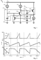
- FIG 1 is a schematic circuit diagram of an example embodiment of an oscillator 100.
- the oscillator 100 comprises first, second and third charging circuits 101, 102, 103, which are arranged such that each charging circuit is triggered by a preceding charging circuit.
- Charging of the first charging circuit 101 triggers a change in charging of the second charging circuit 102, which triggers a change in charging of the third charging circuit 103, which then triggers a change in charging of the first charging circuit 101, thereby creating an oscillatory response to a voltage supply V DD provided on a voltage supply connection 104.
- Figure 2 is a series of plots showing voltage as a function of time for first, second and third nodes 116, 117, 118 in the circuit 100 of Figure 1 .
- Voltage traces 201, 202, 203 are for the first, second and third nodes 116, 117, 118 respectively at a low temperature
- voltage traces 204, 205, 206 are for the first, second and third nodes 116, 117, 118 respectively at a high temperature.
- Each charging circuit 101, 102, 103 comprises a transistor 106, 109, 111 and a capacitor 107, 110, 112.
- Each capacitor 107, 110, 112 is charged or discharged by an associated current source 113, 114, 115.
- the first capacitor 107 is connected between the first current source 113 and the common connection 105 (which may alternatively be termed a ground connection in some embodiments), and is charged by current flow through the first current source 113.
- the second capacitor 110 is connected between the second current source 114 and the common connection 105, and is arranged to be charged by current flow through the second current source 114.
- the third capacitor 112 is connected between the common connection 105 and the third current source 115, which is arranged to discharge the third capacitor 112 when the second transistor 109 is not conducting.
- Each transistor 106, 109, 111 is arranged to change states, i.e. to switch on or off, depending on the charge state of (i.e. the voltage across) an associated capacitor 107, 110, 112.
- the first transistor 106 which in the illustrated embodiment is an n-channel MOSFET, switches on, i.e. conducts, if the voltage at the first node 116, which is equal to the voltage across the first capacitor 107, is above its threshold voltage.
- the second transistor 109 which in the illustrated embodiment is a p-channel MOSFET, switches off, i.e.
- the third transistor 111 which in the illustrated embodiment is an n-channel MOSFET, switches on, i.e. conducts, when the voltage at the third node 118, which is equal to the voltage across the third capacitor 112, is above the threshold voltage of the third transistor 111.
- Each of these threshold voltages will vary with temperature.
- the capacitor in each circuit is arranged to be charged or discharged upon a transistor from a preceding charging circuit switching states.
- a cycle may be considered to begin with the first charging circuit 101.
- the first capacitor 107 begins charging upon a current being supplied from the first current source 113.
- a voltage at the first node 116 (voltage traces 201, 204 in Figure 2 ) rises as the first capacitor 107 is charged until the voltage reaches the threshold voltage of the first transistor 106.
- the first transistor 106 then switches state, i.e. begins to conduct.
- the second capacitor 110 is also charging, as it is supplied by the second current source 114. Once the first transistor 106 switches state and begins to conduct, the second capacitor 110 begins to discharge.
- the second transistor 109 switches states, i.e. starts conducting. This then causes the third capacitor 112 to rapidly charge, raising the voltage at the third node 118 (voltage traces 203, 206) above the threshold voltage of the third transistor 111, resulting in the first capacitor 107 discharging and being kept discharged while this voltage is kept high. As a result of the first capacitor 107 being discharged, the first transistor 106 switches off and the second capacitor 110 begins to charge again.
- the second transistor 109 switches state, i.e. stops conducting, causing charge across the third capacitor 112 to be drawn away to the common connection via the third current source 115.
- the third transistor 111 stops conducting and the cycle begins again with the first capacitor 107 beginning to charge.
- the behaviour of the oscillator 100 will change as the temperature changes.
- the threshold voltages of the first and third transistors 106, 111 decreases, thereby decreasing the time taken for the transistors to switch states, tending to increase the frequency of oscillation.
- the threshold voltage of the second transistor 109 also decreases with increasing temperature, which results in the time taken for the second capacitor 110 to charge up until the second transistor switches state to turn off being longer, tending to decrease the frequency of oscillation.
- the relative weightings of the different charging circuits can therefore be chosen to compensate for temperature, for example by selecting appropriate values for the capacitors 107, 110, 112 and the currents supplied by the current sources 113, 114, 115.
- Selecting suitable values can thereby maintain the frequency at which the oscillator 100 operates to be within a defined range over a defined temperature range.
- the time period for each oscillation is roughly equal at high and low temperatures, indicating that the oscillator is compensated for temperature.
- Figure 3 is a plot of frequency and supply voltage as a function of temperature for an example embodiment in which compensation is made to take account of changes in threshold voltage and in the supply voltage V DD , which falls with increasing temperature.
- the oscillation frequency f is maintained within the range of 1.24 to 1.32 MHz over a temperature range of - 50 to 100 °C, and varies by a smaller amount, within around 1.3 to 1.32 MHz, over an expected operating temperature range of between -25 and 50 °C.
- the oscillation frequency of the oscillator varies by less than 2% over the temperature range of -25 and 50 °C, while the supply voltage over this range is less than 700 mV.
- Example current values for the oscillator circuit as described above are 25nA, 12.5nA and 50nA for current sources 113, 114, 115 respectively.
- Each of the capacitance values will typically be in the fF range, and may be mostly determined by the intrinsic capacitances of the transistors and associated parasitic components due to interconnects.
- One or more of the capacitors may, however, be determined by incorporating a capacitive element.
- Capacitor 110 which may have a capacitance of around 2.15 fF in an example embodiment may be determined by a separate capacitive element.
- FIG 4 is a circuit diagram of an example clock signal output module 400 for connection to the oscillator of Figure 1 .
- the module 400 connects to node 118, which supplies the signal 203, 206 shown in Figure 2 .
- This signal is used as a clock pulse input CP to a D-type flip-flop or latch 401, which divides the signal by two to generate a clock signal clk, clk_n having a duty cycle close to 50%.
Landscapes
- Engineering & Computer Science (AREA)
- Computer Hardware Design (AREA)
- Microelectronics & Electronic Packaging (AREA)
- Physics & Mathematics (AREA)
- General Physics & Mathematics (AREA)
- Theoretical Computer Science (AREA)
- Inductance-Capacitance Distribution Constants And Capacitance-Resistance Oscillators (AREA)
- Oscillators With Electromechanical Resonators (AREA)
Priority Applications (3)
| Application Number | Priority Date | Filing Date | Title |
|---|---|---|---|
| EP16153092.8A EP3200347B1 (fr) | 2016-01-28 | 2016-01-28 | Oscillateur compensé en température |
| CN201710007204.1A CN107017841B (zh) | 2016-01-28 | 2017-01-05 | 温度补偿振荡器 |
| US15/418,719 US10032106B2 (en) | 2016-01-28 | 2017-01-28 | Temperature-compensated oscillator |
Applications Claiming Priority (1)
| Application Number | Priority Date | Filing Date | Title |
|---|---|---|---|
| EP16153092.8A EP3200347B1 (fr) | 2016-01-28 | 2016-01-28 | Oscillateur compensé en température |
Publications (2)
| Publication Number | Publication Date |
|---|---|
| EP3200347A1 true EP3200347A1 (fr) | 2017-08-02 |
| EP3200347B1 EP3200347B1 (fr) | 2019-11-13 |
Family
ID=55237606
Family Applications (1)
| Application Number | Title | Priority Date | Filing Date |
|---|---|---|---|
| EP16153092.8A Active EP3200347B1 (fr) | 2016-01-28 | 2016-01-28 | Oscillateur compensé en température |
Country Status (3)
| Country | Link |
|---|---|
| US (1) | US10032106B2 (fr) |
| EP (1) | EP3200347B1 (fr) |
| CN (1) | CN107017841B (fr) |
Families Citing this family (9)
| Publication number | Priority date | Publication date | Assignee | Title |
|---|---|---|---|---|
| US10304522B2 (en) | 2017-01-31 | 2019-05-28 | International Business Machines Corporation | Method for low power operation and test using DRAM device |
| US9916890B1 (en) | 2017-02-21 | 2018-03-13 | International Business Machines Corporation | Predicting data correlation using multivalued logical outputs in static random access memory (SRAM) storage cells |
| US10598710B2 (en) | 2017-06-02 | 2020-03-24 | International Business Machines Corporation | Cognitive analysis using applied analog circuits |
| US10663502B2 (en) | 2017-06-02 | 2020-05-26 | International Business Machines Corporation | Real time cognitive monitoring of correlations between variables |
| US10037792B1 (en) * | 2017-06-02 | 2018-07-31 | International Business Machines Corporation | Optimizing data approximation analysis using low power circuitry |
| US11526768B2 (en) | 2017-06-02 | 2022-12-13 | International Business Machines Corporation | Real time cognitive reasoning using a circuit with varying confidence level alerts |
| CN110162430B (zh) * | 2018-02-13 | 2021-11-09 | 华为技术有限公司 | 一种温度自适应方法、装置及设备 |
| US11437981B1 (en) | 2021-03-31 | 2022-09-06 | Nxp B.V. | Temperature compensated auto tunable frequency locked loop oscillator |
| US12483192B2 (en) | 2023-05-17 | 2025-11-25 | Nxp Usa, Inc. | Temperature compensation in oscillator circuits |
Citations (5)
| Publication number | Priority date | Publication date | Assignee | Title |
|---|---|---|---|---|
| US20040217821A1 (en) * | 2003-04-29 | 2004-11-04 | Chien-Hung Ho | Ring oscillator having a stable output signal without influence of mos devices |
| US20090160562A1 (en) * | 2007-12-19 | 2009-06-25 | Hsien-Sheng Huang | Oscillating device |
| US7581881B2 (en) * | 2006-01-11 | 2009-09-01 | Samsung Electronics Co., Ltd. | Temperature sensor using ring oscillator and temperature detection method using the same |
| US20100066434A1 (en) * | 2008-09-18 | 2010-03-18 | Holtek Semiconductor Inc. | Temperature compensating circuit and method |
| US20110175684A1 (en) * | 2010-01-19 | 2011-07-21 | Elite Semiconductor Memory Technology Inc. | Temperature-compensated ring oscillator |
Family Cites Families (12)
| Publication number | Priority date | Publication date | Assignee | Title |
|---|---|---|---|---|
| US3978431A (en) * | 1975-07-03 | 1976-08-31 | Motorola, Inc. | Temperature compensated oscillator |
| EP0744836A3 (fr) * | 1995-05-25 | 1998-03-25 | Kabushiki Kaisha Meidensha | Oscillateur à cristal compensé en température |
| KR0134914B1 (ko) * | 1995-06-29 | 1998-04-25 | 김광호 | 아날로그 방식의 발진회로 |
| JPH1056329A (ja) * | 1996-08-12 | 1998-02-24 | Matsushita Electric Ind Co Ltd | 周波数制御発振器 |
| US5764111A (en) * | 1997-02-18 | 1998-06-09 | Motorola Inc. | Voltage controlled ring oscillator frequency multiplier |
| CN2794038Y (zh) * | 2005-06-03 | 2006-07-05 | Bcd半导体制造有限公司 | 用于振荡器的温度系数补偿电路及使用该电路的振荡器 |
| JP4949265B2 (ja) * | 2005-11-07 | 2012-06-06 | シチズンホールディングス株式会社 | 温度補償型発振器およびその製造方法 |
| KR100753666B1 (ko) * | 2006-06-01 | 2007-08-31 | 삼성전기주식회사 | 초저전력 rc 발진기 |
| US7432771B2 (en) * | 2006-06-02 | 2008-10-07 | Smartech Worldwide Limited | Oscillator circuit having temperature and supply voltage compensation |
| KR100886993B1 (ko) * | 2006-12-27 | 2009-03-04 | 재단법인서울대학교산학협력재단 | 온도 보상 기능을 갖춘 cmos 발진기 및 그 보상 방법 |
| KR101104720B1 (ko) * | 2009-11-30 | 2012-01-11 | 이타칩스 주식회사 | 외부공급전압, 온도 및 공정에 대한 보상을 갖는 오실레이터 회로 |
| US8810284B2 (en) * | 2012-12-11 | 2014-08-19 | Sandisk Technologies Inc. | Voltage and temperature compensated frequency converter |
-
2016
- 2016-01-28 EP EP16153092.8A patent/EP3200347B1/fr active Active
-
2017
- 2017-01-05 CN CN201710007204.1A patent/CN107017841B/zh not_active Expired - Fee Related
- 2017-01-28 US US15/418,719 patent/US10032106B2/en active Active
Patent Citations (5)
| Publication number | Priority date | Publication date | Assignee | Title |
|---|---|---|---|---|
| US20040217821A1 (en) * | 2003-04-29 | 2004-11-04 | Chien-Hung Ho | Ring oscillator having a stable output signal without influence of mos devices |
| US7581881B2 (en) * | 2006-01-11 | 2009-09-01 | Samsung Electronics Co., Ltd. | Temperature sensor using ring oscillator and temperature detection method using the same |
| US20090160562A1 (en) * | 2007-12-19 | 2009-06-25 | Hsien-Sheng Huang | Oscillating device |
| US20100066434A1 (en) * | 2008-09-18 | 2010-03-18 | Holtek Semiconductor Inc. | Temperature compensating circuit and method |
| US20110175684A1 (en) * | 2010-01-19 | 2011-07-21 | Elite Semiconductor Memory Technology Inc. | Temperature-compensated ring oscillator |
Also Published As
| Publication number | Publication date |
|---|---|
| EP3200347B1 (fr) | 2019-11-13 |
| US10032106B2 (en) | 2018-07-24 |
| US20170220918A1 (en) | 2017-08-03 |
| CN107017841A (zh) | 2017-08-04 |
| CN107017841B (zh) | 2022-08-09 |
Similar Documents
| Publication | Publication Date | Title |
|---|---|---|
| US10032106B2 (en) | Temperature-compensated oscillator | |
| JP3594631B2 (ja) | 電源に対して補償されたmos発振回路 | |
| US6388479B1 (en) | Oscillator based power-on-reset circuit | |
| US20050195676A1 (en) | Level shift circuit and semiconductor device | |
| US8970313B2 (en) | Area efficient single capacitor CMOS relaxation oscillator | |
| CN115622548B (zh) | 一种高边nmos浮地驱动电路 | |
| US12388445B2 (en) | Level shift circuit | |
| CN113691220B (zh) | 片上低频振荡器 | |
| US11290057B2 (en) | Oscillation circuit | |
| JP7272152B2 (ja) | バイアス電流回路、発振回路 | |
| US9461630B1 (en) | Low current and high frequency oscillator circuit | |
| US11683010B2 (en) | Oscillation circuit | |
| KR101986799B1 (ko) | 저전력과 작은 면적으로 구현한 단일 비교기 구조의 릴렉세이션 발진기 | |
| US12556167B2 (en) | Oscillator circuit | |
| US5982247A (en) | CR oscillating circuit | |
| KR100201719B1 (ko) | 랫치업 방지회로를 갖춘 반도체 집적회로 | |
| WO2007042970A1 (fr) | Amplificateur/tampon du type a seuil unique et a conductivite unique | |
| US12021522B2 (en) | Quasi-adiabatic logic circuits | |
| CN115104257B (zh) | 低功率电子振荡器 | |
| US20230056841A1 (en) | Low power oscillator with variable duty cycle and method therefor | |
| US11949409B2 (en) | Low-power pulse output circuit | |
| US20250279768A1 (en) | Oscillator with leakage current compensation function | |
| US10700637B2 (en) | Oscillator circuits capable of compensating for PVT variations | |
| US7071761B1 (en) | Apparatus and method for reducing propagation delay | |
| US20100231273A1 (en) | Semiconductor device |
Legal Events
| Date | Code | Title | Description |
|---|---|---|---|
| PUAI | Public reference made under article 153(3) epc to a published international application that has entered the european phase |
Free format text: ORIGINAL CODE: 0009012 |
|
| STAA | Information on the status of an ep patent application or granted ep patent |
Free format text: STATUS: THE APPLICATION HAS BEEN PUBLISHED |
|
| AK | Designated contracting states |
Kind code of ref document: A1 Designated state(s): AL AT BE BG CH CY CZ DE DK EE ES FI FR GB GR HR HU IE IS IT LI LT LU LV MC MK MT NL NO PL PT RO RS SE SI SK SM TR |
|
| AX | Request for extension of the european patent |
Extension state: BA ME |
|
| STAA | Information on the status of an ep patent application or granted ep patent |
Free format text: STATUS: REQUEST FOR EXAMINATION WAS MADE |
|
| 17P | Request for examination filed |
Effective date: 20180202 |
|
| RBV | Designated contracting states (corrected) |
Designated state(s): AL AT BE BG CH CY CZ DE DK EE ES FI FR GB GR HR HU IE IS IT LI LT LU LV MC MK MT NL NO PL PT RO RS SE SI SK SM TR |
|
| REG | Reference to a national code |
Ref country code: DE Ref legal event code: R079 Ref document number: 602016024118 Country of ref document: DE Free format text: PREVIOUS MAIN CLASS: H03K0003030000 Ipc: G06K0019077000 |
|
| GRAP | Despatch of communication of intention to grant a patent |
Free format text: ORIGINAL CODE: EPIDOSNIGR1 |
|
| STAA | Information on the status of an ep patent application or granted ep patent |
Free format text: STATUS: GRANT OF PATENT IS INTENDED |
|
| RIC1 | Information provided on ipc code assigned before grant |
Ipc: G06K 19/077 20060101AFI20190215BHEP Ipc: H03K 3/011 20060101ALI20190215BHEP Ipc: H03K 3/03 20060101ALI20190215BHEP Ipc: H03L 1/04 20060101ALI20190215BHEP |
|
| INTG | Intention to grant announced |
Effective date: 20190308 |
|
| GRAJ | Information related to disapproval of communication of intention to grant by the applicant or resumption of examination proceedings by the epo deleted |
Free format text: ORIGINAL CODE: EPIDOSDIGR1 |
|
| STAA | Information on the status of an ep patent application or granted ep patent |
Free format text: STATUS: REQUEST FOR EXAMINATION WAS MADE |
|
| GRAP | Despatch of communication of intention to grant a patent |
Free format text: ORIGINAL CODE: EPIDOSNIGR1 |
|
| STAA | Information on the status of an ep patent application or granted ep patent |
Free format text: STATUS: GRANT OF PATENT IS INTENDED |
|
| INTC | Intention to grant announced (deleted) | ||
| INTG | Intention to grant announced |
Effective date: 20190709 |
|
| GRAS | Grant fee paid |
Free format text: ORIGINAL CODE: EPIDOSNIGR3 |
|
| GRAA | (expected) grant |
Free format text: ORIGINAL CODE: 0009210 |
|
| STAA | Information on the status of an ep patent application or granted ep patent |
Free format text: STATUS: THE PATENT HAS BEEN GRANTED |
|
| AK | Designated contracting states |
Kind code of ref document: B1 Designated state(s): AL AT BE BG CH CY CZ DE DK EE ES FI FR GB GR HR HU IE IS IT LI LT LU LV MC MK MT NL NO PL PT RO RS SE SI SK SM TR |
|
| REG | Reference to a national code |
Ref country code: CH Ref legal event code: EP Ref country code: AT Ref legal event code: REF Ref document number: 1202444 Country of ref document: AT Kind code of ref document: T Effective date: 20191115 |
|
| REG | Reference to a national code |
Ref country code: DE Ref legal event code: R096 Ref document number: 602016024118 Country of ref document: DE |
|
| REG | Reference to a national code |
Ref country code: IE Ref legal event code: FG4D |
|
| REG | Reference to a national code |
Ref country code: NL Ref legal event code: MP Effective date: 20191113 |
|
| REG | Reference to a national code |
Ref country code: LT Ref legal event code: MG4D |
|
| PG25 | Lapsed in a contracting state [announced via postgrant information from national office to epo] |
Ref country code: BG Free format text: LAPSE BECAUSE OF FAILURE TO SUBMIT A TRANSLATION OF THE DESCRIPTION OR TO PAY THE FEE WITHIN THE PRESCRIBED TIME-LIMIT Effective date: 20200213 Ref country code: FI Free format text: LAPSE BECAUSE OF FAILURE TO SUBMIT A TRANSLATION OF THE DESCRIPTION OR TO PAY THE FEE WITHIN THE PRESCRIBED TIME-LIMIT Effective date: 20191113 Ref country code: NL Free format text: LAPSE BECAUSE OF FAILURE TO SUBMIT A TRANSLATION OF THE DESCRIPTION OR TO PAY THE FEE WITHIN THE PRESCRIBED TIME-LIMIT Effective date: 20191113 Ref country code: SE Free format text: LAPSE BECAUSE OF FAILURE TO SUBMIT A TRANSLATION OF THE DESCRIPTION OR TO PAY THE FEE WITHIN THE PRESCRIBED TIME-LIMIT Effective date: 20191113 Ref country code: LV Free format text: LAPSE BECAUSE OF FAILURE TO SUBMIT A TRANSLATION OF THE DESCRIPTION OR TO PAY THE FEE WITHIN THE PRESCRIBED TIME-LIMIT Effective date: 20191113 Ref country code: PT Free format text: LAPSE BECAUSE OF FAILURE TO SUBMIT A TRANSLATION OF THE DESCRIPTION OR TO PAY THE FEE WITHIN THE PRESCRIBED TIME-LIMIT Effective date: 20200313 Ref country code: GR Free format text: LAPSE BECAUSE OF FAILURE TO SUBMIT A TRANSLATION OF THE DESCRIPTION OR TO PAY THE FEE WITHIN THE PRESCRIBED TIME-LIMIT Effective date: 20200214 Ref country code: NO Free format text: LAPSE BECAUSE OF FAILURE TO SUBMIT A TRANSLATION OF THE DESCRIPTION OR TO PAY THE FEE WITHIN THE PRESCRIBED TIME-LIMIT Effective date: 20200213 Ref country code: PL Free format text: LAPSE BECAUSE OF FAILURE TO SUBMIT A TRANSLATION OF THE DESCRIPTION OR TO PAY THE FEE WITHIN THE PRESCRIBED TIME-LIMIT Effective date: 20191113 Ref country code: LT Free format text: LAPSE BECAUSE OF FAILURE TO SUBMIT A TRANSLATION OF THE DESCRIPTION OR TO PAY THE FEE WITHIN THE PRESCRIBED TIME-LIMIT Effective date: 20191113 |
|
| PG25 | Lapsed in a contracting state [announced via postgrant information from national office to epo] |
Ref country code: IS Free format text: LAPSE BECAUSE OF FAILURE TO SUBMIT A TRANSLATION OF THE DESCRIPTION OR TO PAY THE FEE WITHIN THE PRESCRIBED TIME-LIMIT Effective date: 20200313 Ref country code: HR Free format text: LAPSE BECAUSE OF FAILURE TO SUBMIT A TRANSLATION OF THE DESCRIPTION OR TO PAY THE FEE WITHIN THE PRESCRIBED TIME-LIMIT Effective date: 20191113 Ref country code: RS Free format text: LAPSE BECAUSE OF FAILURE TO SUBMIT A TRANSLATION OF THE DESCRIPTION OR TO PAY THE FEE WITHIN THE PRESCRIBED TIME-LIMIT Effective date: 20191113 |
|
| PG25 | Lapsed in a contracting state [announced via postgrant information from national office to epo] |
Ref country code: AL Free format text: LAPSE BECAUSE OF FAILURE TO SUBMIT A TRANSLATION OF THE DESCRIPTION OR TO PAY THE FEE WITHIN THE PRESCRIBED TIME-LIMIT Effective date: 20191113 |
|
| PG25 | Lapsed in a contracting state [announced via postgrant information from national office to epo] |
Ref country code: DK Free format text: LAPSE BECAUSE OF FAILURE TO SUBMIT A TRANSLATION OF THE DESCRIPTION OR TO PAY THE FEE WITHIN THE PRESCRIBED TIME-LIMIT Effective date: 20191113 Ref country code: EE Free format text: LAPSE BECAUSE OF FAILURE TO SUBMIT A TRANSLATION OF THE DESCRIPTION OR TO PAY THE FEE WITHIN THE PRESCRIBED TIME-LIMIT Effective date: 20191113 Ref country code: ES Free format text: LAPSE BECAUSE OF FAILURE TO SUBMIT A TRANSLATION OF THE DESCRIPTION OR TO PAY THE FEE WITHIN THE PRESCRIBED TIME-LIMIT Effective date: 20191113 Ref country code: RO Free format text: LAPSE BECAUSE OF FAILURE TO SUBMIT A TRANSLATION OF THE DESCRIPTION OR TO PAY THE FEE WITHIN THE PRESCRIBED TIME-LIMIT Effective date: 20191113 Ref country code: CZ Free format text: LAPSE BECAUSE OF FAILURE TO SUBMIT A TRANSLATION OF THE DESCRIPTION OR TO PAY THE FEE WITHIN THE PRESCRIBED TIME-LIMIT Effective date: 20191113 |
|
| REG | Reference to a national code |
Ref country code: DE Ref legal event code: R097 Ref document number: 602016024118 Country of ref document: DE |
|
| REG | Reference to a national code |
Ref country code: AT Ref legal event code: MK05 Ref document number: 1202444 Country of ref document: AT Kind code of ref document: T Effective date: 20191113 |
|
| PG25 | Lapsed in a contracting state [announced via postgrant information from national office to epo] |
Ref country code: SK Free format text: LAPSE BECAUSE OF FAILURE TO SUBMIT A TRANSLATION OF THE DESCRIPTION OR TO PAY THE FEE WITHIN THE PRESCRIBED TIME-LIMIT Effective date: 20191113 Ref country code: SM Free format text: LAPSE BECAUSE OF FAILURE TO SUBMIT A TRANSLATION OF THE DESCRIPTION OR TO PAY THE FEE WITHIN THE PRESCRIBED TIME-LIMIT Effective date: 20191113 Ref country code: MC Free format text: LAPSE BECAUSE OF FAILURE TO SUBMIT A TRANSLATION OF THE DESCRIPTION OR TO PAY THE FEE WITHIN THE PRESCRIBED TIME-LIMIT Effective date: 20191113 |
|
| REG | Reference to a national code |
Ref country code: CH Ref legal event code: PL |
|
| PLBE | No opposition filed within time limit |
Free format text: ORIGINAL CODE: 0009261 |
|
| STAA | Information on the status of an ep patent application or granted ep patent |
Free format text: STATUS: NO OPPOSITION FILED WITHIN TIME LIMIT |
|
| REG | Reference to a national code |
Ref country code: BE Ref legal event code: MM Effective date: 20200131 |
|
| 26N | No opposition filed |
Effective date: 20200814 |
|
| GBPC | Gb: european patent ceased through non-payment of renewal fee |
Effective date: 20200213 |
|
| PG25 | Lapsed in a contracting state [announced via postgrant information from national office to epo] |
Ref country code: LU Free format text: LAPSE BECAUSE OF NON-PAYMENT OF DUE FEES Effective date: 20200128 |
|
| PG25 | Lapsed in a contracting state [announced via postgrant information from national office to epo] |
Ref country code: CH Free format text: LAPSE BECAUSE OF NON-PAYMENT OF DUE FEES Effective date: 20200131 Ref country code: AT Free format text: LAPSE BECAUSE OF FAILURE TO SUBMIT A TRANSLATION OF THE DESCRIPTION OR TO PAY THE FEE WITHIN THE PRESCRIBED TIME-LIMIT Effective date: 20191113 Ref country code: SI Free format text: LAPSE BECAUSE OF FAILURE TO SUBMIT A TRANSLATION OF THE DESCRIPTION OR TO PAY THE FEE WITHIN THE PRESCRIBED TIME-LIMIT Effective date: 20191113 Ref country code: BE Free format text: LAPSE BECAUSE OF NON-PAYMENT OF DUE FEES Effective date: 20200131 Ref country code: LI Free format text: LAPSE BECAUSE OF NON-PAYMENT OF DUE FEES Effective date: 20200131 |
|
| PG25 | Lapsed in a contracting state [announced via postgrant information from national office to epo] |
Ref country code: GB Free format text: LAPSE BECAUSE OF NON-PAYMENT OF DUE FEES Effective date: 20200213 Ref country code: IT Free format text: LAPSE BECAUSE OF FAILURE TO SUBMIT A TRANSLATION OF THE DESCRIPTION OR TO PAY THE FEE WITHIN THE PRESCRIBED TIME-LIMIT Effective date: 20191113 Ref country code: IE Free format text: LAPSE BECAUSE OF NON-PAYMENT OF DUE FEES Effective date: 20200128 |
|
| PG25 | Lapsed in a contracting state [announced via postgrant information from national office to epo] |
Ref country code: FR Free format text: LAPSE BECAUSE OF NON-PAYMENT OF DUE FEES Effective date: 20200131 |
|
| PG25 | Lapsed in a contracting state [announced via postgrant information from national office to epo] |
Ref country code: TR Free format text: LAPSE BECAUSE OF FAILURE TO SUBMIT A TRANSLATION OF THE DESCRIPTION OR TO PAY THE FEE WITHIN THE PRESCRIBED TIME-LIMIT Effective date: 20191113 Ref country code: MT Free format text: LAPSE BECAUSE OF FAILURE TO SUBMIT A TRANSLATION OF THE DESCRIPTION OR TO PAY THE FEE WITHIN THE PRESCRIBED TIME-LIMIT Effective date: 20191113 Ref country code: CY Free format text: LAPSE BECAUSE OF FAILURE TO SUBMIT A TRANSLATION OF THE DESCRIPTION OR TO PAY THE FEE WITHIN THE PRESCRIBED TIME-LIMIT Effective date: 20191113 |
|
| PG25 | Lapsed in a contracting state [announced via postgrant information from national office to epo] |
Ref country code: MK Free format text: LAPSE BECAUSE OF FAILURE TO SUBMIT A TRANSLATION OF THE DESCRIPTION OR TO PAY THE FEE WITHIN THE PRESCRIBED TIME-LIMIT Effective date: 20191113 |
|
| PGFP | Annual fee paid to national office [announced via postgrant information from national office to epo] |
Ref country code: DE Payment date: 20221220 Year of fee payment: 8 |
|
| P01 | Opt-out of the competence of the unified patent court (upc) registered |
Effective date: 20230725 |
|
| REG | Reference to a national code |
Ref country code: DE Ref legal event code: R119 Ref document number: 602016024118 Country of ref document: DE |
|
| PG25 | Lapsed in a contracting state [announced via postgrant information from national office to epo] |
Ref country code: DE Free format text: LAPSE BECAUSE OF NON-PAYMENT OF DUE FEES Effective date: 20240801 |
|
| PG25 | Lapsed in a contracting state [announced via postgrant information from national office to epo] |
Ref country code: DE Free format text: LAPSE BECAUSE OF NON-PAYMENT OF DUE FEES Effective date: 20240801 |