EP3200568B1 - Élément de liaison pour batterie et procédé d'activation d'un dispositif électronique - Google Patents
Élément de liaison pour batterie et procédé d'activation d'un dispositif électronique Download PDFInfo
- Publication number
- EP3200568B1 EP3200568B1 EP17151706.3A EP17151706A EP3200568B1 EP 3200568 B1 EP3200568 B1 EP 3200568B1 EP 17151706 A EP17151706 A EP 17151706A EP 3200568 B1 EP3200568 B1 EP 3200568B1
- Authority
- EP
- European Patent Office
- Prior art keywords
- contact element
- battery bridge
- air gap
- insulator
- battery
- Prior art date
- Legal status (The legal status is an assumption and is not a legal conclusion. Google has not performed a legal analysis and makes no representation as to the accuracy of the status listed.)
- Active
Links
Images


Classifications
-
- B—PERFORMING OPERATIONS; TRANSPORTING
- B23—MACHINE TOOLS; METAL-WORKING NOT OTHERWISE PROVIDED FOR
- B23K—SOLDERING OR UNSOLDERING; WELDING; CLADDING OR PLATING BY SOLDERING OR WELDING; CUTTING BY APPLYING HEAT LOCALLY, e.g. FLAME CUTTING; WORKING BY LASER BEAM
- B23K26/00—Working by laser beam, e.g. welding, cutting or boring
- B23K26/20—Bonding
- B23K26/21—Bonding by welding
- B23K26/22—Spot welding
-
- H—ELECTRICITY
- H01—ELECTRIC ELEMENTS
- H01R—ELECTRICALLY-CONDUCTIVE CONNECTIONS; STRUCTURAL ASSOCIATIONS OF A PLURALITY OF MUTUALLY-INSULATED ELECTRICAL CONNECTING ELEMENTS; COUPLING DEVICES; CURRENT COLLECTORS
- H01R11/00—Individual connecting elements providing two or more spaced connecting locations for conductive members which are, or may be, thereby interconnected, e.g. end pieces for wires or cables supported by the wire or cable and having means for facilitating electrical connection to some other wire, terminal, or conductive member, blocks of binding posts
- H01R11/01—Individual connecting elements providing two or more spaced connecting locations for conductive members which are, or may be, thereby interconnected, e.g. end pieces for wires or cables supported by the wire or cable and having means for facilitating electrical connection to some other wire, terminal, or conductive member, blocks of binding posts characterised by the form or arrangement of the conductive interconnection between the connecting locations
-
- A—HUMAN NECESSITIES
- A61—MEDICAL OR VETERINARY SCIENCE; HYGIENE
- A61N—ELECTROTHERAPY; MAGNETOTHERAPY; RADIATION THERAPY; ULTRASOUND THERAPY
- A61N1/00—Electrotherapy; Circuits therefor
- A61N1/18—Applying electric currents by contact electrodes
- A61N1/32—Applying electric currents by contact electrodes alternating or intermittent currents
- A61N1/36—Applying electric currents by contact electrodes alternating or intermittent currents for stimulation
- A61N1/372—Arrangements in connection with the implantation of stimulators
- A61N1/375—Constructional arrangements, e.g. casings
- A61N1/3758—Packaging of the components within the casing
-
- B—PERFORMING OPERATIONS; TRANSPORTING
- B23—MACHINE TOOLS; METAL-WORKING NOT OTHERWISE PROVIDED FOR
- B23K—SOLDERING OR UNSOLDERING; WELDING; CLADDING OR PLATING BY SOLDERING OR WELDING; CUTTING BY APPLYING HEAT LOCALLY, e.g. FLAME CUTTING; WORKING BY LASER BEAM
- B23K26/00—Working by laser beam, e.g. welding, cutting or boring
- B23K26/20—Bonding
- B23K26/21—Bonding by welding
- B23K26/24—Seam welding
- B23K26/242—Fillet welding, i.e. involving a weld of substantially triangular cross section joining two parts
-
- B—PERFORMING OPERATIONS; TRANSPORTING
- B23—MACHINE TOOLS; METAL-WORKING NOT OTHERWISE PROVIDED FOR
- B23K—SOLDERING OR UNSOLDERING; WELDING; CLADDING OR PLATING BY SOLDERING OR WELDING; CUTTING BY APPLYING HEAT LOCALLY, e.g. FLAME CUTTING; WORKING BY LASER BEAM
- B23K26/00—Working by laser beam, e.g. welding, cutting or boring
- B23K26/20—Bonding
- B23K26/21—Bonding by welding
- B23K26/24—Seam welding
- B23K26/28—Seam welding of curved planar seams
-
- B—PERFORMING OPERATIONS; TRANSPORTING
- B23—MACHINE TOOLS; METAL-WORKING NOT OTHERWISE PROVIDED FOR
- B23K—SOLDERING OR UNSOLDERING; WELDING; CLADDING OR PLATING BY SOLDERING OR WELDING; CUTTING BY APPLYING HEAT LOCALLY, e.g. FLAME CUTTING; WORKING BY LASER BEAM
- B23K26/00—Working by laser beam, e.g. welding, cutting or boring
- B23K26/20—Bonding
- B23K26/32—Bonding taking account of the properties of the material involved
-
- H—ELECTRICITY
- H01—ELECTRIC ELEMENTS
- H01R—ELECTRICALLY-CONDUCTIVE CONNECTIONS; STRUCTURAL ASSOCIATIONS OF A PLURALITY OF MUTUALLY-INSULATED ELECTRICAL CONNECTING ELEMENTS; COUPLING DEVICES; CURRENT COLLECTORS
- H01R43/00—Apparatus or processes specially adapted for manufacturing, assembling, maintaining, or repairing of line connectors or current collectors or for joining electric conductors
- H01R43/02—Apparatus or processes specially adapted for manufacturing, assembling, maintaining, or repairing of line connectors or current collectors or for joining electric conductors for soldered or welded connections
- H01R43/0221—Laser welding
-
- H—ELECTRICITY
- H05—ELECTRIC TECHNIQUES NOT OTHERWISE PROVIDED FOR
- H05K—PRINTED CIRCUITS; CASINGS OR CONSTRUCTIONAL DETAILS OF ELECTRIC APPARATUS; MANUFACTURE OF ASSEMBLAGES OF ELECTRICAL COMPONENTS
- H05K1/00—Printed circuits
- H05K1/02—Details
- H05K1/0286—Programmable, customizable or modifiable circuits
- H05K1/0293—Individual printed conductors which are adapted for modification, e.g. fusable or breakable conductors, printed switches
-
- H—ELECTRICITY
- H05—ELECTRIC TECHNIQUES NOT OTHERWISE PROVIDED FOR
- H05K—PRINTED CIRCUITS; CASINGS OR CONSTRUCTIONAL DETAILS OF ELECTRIC APPARATUS; MANUFACTURE OF ASSEMBLAGES OF ELECTRICAL COMPONENTS
- H05K3/00—Apparatus or processes for manufacturing printed circuits
- H05K3/30—Assembling printed circuits with electric components, e.g. with resistors
- H05K3/32—Assembling printed circuits with electric components, e.g. with resistors electrically connecting electric components or wires to printed circuits
- H05K3/328—Assembling printed circuits with electric components, e.g. with resistors electrically connecting electric components or wires to printed circuits by welding
-
- B—PERFORMING OPERATIONS; TRANSPORTING
- B23—MACHINE TOOLS; METAL-WORKING NOT OTHERWISE PROVIDED FOR
- B23K—SOLDERING OR UNSOLDERING; WELDING; CLADDING OR PLATING BY SOLDERING OR WELDING; CUTTING BY APPLYING HEAT LOCALLY, e.g. FLAME CUTTING; WORKING BY LASER BEAM
- B23K2101/00—Articles made by soldering, welding or cutting
- B23K2101/36—Electric or electronic devices
- B23K2101/38—Conductors
-
- H—ELECTRICITY
- H01—ELECTRIC ELEMENTS
- H01R—ELECTRICALLY-CONDUCTIVE CONNECTIONS; STRUCTURAL ASSOCIATIONS OF A PLURALITY OF MUTUALLY-INSULATED ELECTRICAL CONNECTING ELEMENTS; COUPLING DEVICES; CURRENT COLLECTORS
- H01R4/00—Electrically-conductive connections between two or more conductive members in direct contact, i.e. touching one another; Means for effecting or maintaining such contact; Electrically-conductive connections having two or more spaced connecting locations for conductors and using contact members penetrating insulation
- H01R4/02—Soldered or welded connections
- H01R4/029—Welded connections
-
- H—ELECTRICITY
- H05—ELECTRIC TECHNIQUES NOT OTHERWISE PROVIDED FOR
- H05K—PRINTED CIRCUITS; CASINGS OR CONSTRUCTIONAL DETAILS OF ELECTRIC APPARATUS; MANUFACTURE OF ASSEMBLAGES OF ELECTRICAL COMPONENTS
- H05K2201/00—Indexing scheme relating to printed circuits covered by H05K1/00
- H05K2201/10—Details of components or other objects attached to or integrated in a printed circuit board
- H05K2201/10007—Types of components
- H05K2201/10053—Switch
-
- H—ELECTRICITY
- H05—ELECTRIC TECHNIQUES NOT OTHERWISE PROVIDED FOR
- H05K—PRINTED CIRCUITS; CASINGS OR CONSTRUCTIONAL DETAILS OF ELECTRIC APPARATUS; MANUFACTURE OF ASSEMBLAGES OF ELECTRICAL COMPONENTS
- H05K2201/00—Indexing scheme relating to printed circuits covered by H05K1/00
- H05K2201/10—Details of components or other objects attached to or integrated in a printed circuit board
- H05K2201/10007—Types of components
- H05K2201/10181—Fuse
-
- H—ELECTRICITY
- H05—ELECTRIC TECHNIQUES NOT OTHERWISE PROVIDED FOR
- H05K—PRINTED CIRCUITS; CASINGS OR CONSTRUCTIONAL DETAILS OF ELECTRIC APPARATUS; MANUFACTURE OF ASSEMBLAGES OF ELECTRICAL COMPONENTS
- H05K2201/00—Indexing scheme relating to printed circuits covered by H05K1/00
- H05K2201/10—Details of components or other objects attached to or integrated in a printed circuit board
- H05K2201/10227—Other objects, e.g. metallic pieces
- H05K2201/10242—Metallic cylinders
-
- H—ELECTRICITY
- H05—ELECTRIC TECHNIQUES NOT OTHERWISE PROVIDED FOR
- H05K—PRINTED CIRCUITS; CASINGS OR CONSTRUCTIONAL DETAILS OF ELECTRIC APPARATUS; MANUFACTURE OF ASSEMBLAGES OF ELECTRICAL COMPONENTS
- H05K2201/00—Indexing scheme relating to printed circuits covered by H05K1/00
- H05K2201/10—Details of components or other objects attached to or integrated in a printed circuit board
- H05K2201/10227—Other objects, e.g. metallic pieces
- H05K2201/10363—Jumpers, i.e. non-printed cross-over connections
-
- H—ELECTRICITY
- H05—ELECTRIC TECHNIQUES NOT OTHERWISE PROVIDED FOR
- H05K—PRINTED CIRCUITS; CASINGS OR CONSTRUCTIONAL DETAILS OF ELECTRIC APPARATUS; MANUFACTURE OF ASSEMBLAGES OF ELECTRICAL COMPONENTS
- H05K2201/00—Indexing scheme relating to printed circuits covered by H05K1/00
- H05K2201/10—Details of components or other objects attached to or integrated in a printed circuit board
- H05K2201/10431—Details of mounted components
- H05K2201/10583—Cylindrically shaped component; Fixing means therefore
-
- H—ELECTRICITY
- H05—ELECTRIC TECHNIQUES NOT OTHERWISE PROVIDED FOR
- H05K—PRINTED CIRCUITS; CASINGS OR CONSTRUCTIONAL DETAILS OF ELECTRIC APPARATUS; MANUFACTURE OF ASSEMBLAGES OF ELECTRICAL COMPONENTS
- H05K2203/00—Indexing scheme relating to apparatus or processes for manufacturing printed circuits covered by H05K3/00
- H05K2203/10—Using electric, magnetic and electromagnetic fields; Using laser light
- H05K2203/107—Using laser light
-
- H—ELECTRICITY
- H05—ELECTRIC TECHNIQUES NOT OTHERWISE PROVIDED FOR
- H05K—PRINTED CIRCUITS; CASINGS OR CONSTRUCTIONAL DETAILS OF ELECTRIC APPARATUS; MANUFACTURE OF ASSEMBLAGES OF ELECTRICAL COMPONENTS
- H05K2203/00—Indexing scheme relating to apparatus or processes for manufacturing printed circuits covered by H05K3/00
- H05K2203/17—Post-manufacturing processes
- H05K2203/173—Adding connections between adjacent pads or conductors, e.g. for modifying or repairing
-
- H—ELECTRICITY
- H05—ELECTRIC TECHNIQUES NOT OTHERWISE PROVIDED FOR
- H05K—PRINTED CIRCUITS; CASINGS OR CONSTRUCTIONAL DETAILS OF ELECTRIC APPARATUS; MANUFACTURE OF ASSEMBLAGES OF ELECTRICAL COMPONENTS
- H05K3/00—Apparatus or processes for manufacturing printed circuits
- H05K3/22—Secondary treatment of printed circuits
- H05K3/222—Completing of printed circuits by adding non-printed jumper connections
-
- H—ELECTRICITY
- H05—ELECTRIC TECHNIQUES NOT OTHERWISE PROVIDED FOR
- H05K—PRINTED CIRCUITS; CASINGS OR CONSTRUCTIONAL DETAILS OF ELECTRIC APPARATUS; MANUFACTURE OF ASSEMBLAGES OF ELECTRICAL COMPONENTS
- H05K3/00—Apparatus or processes for manufacturing printed circuits
- H05K3/40—Forming printed elements for providing electric connections to or between printed circuits
- H05K3/4007—Surface contacts, e.g. bumps
- H05K3/4015—Surface contacts, e.g. bumps using auxiliary conductive elements, e.g. pieces of metal foil, metallic spheres
-
- Y—GENERAL TAGGING OF NEW TECHNOLOGICAL DEVELOPMENTS; GENERAL TAGGING OF CROSS-SECTIONAL TECHNOLOGIES SPANNING OVER SEVERAL SECTIONS OF THE IPC; TECHNICAL SUBJECTS COVERED BY FORMER USPC CROSS-REFERENCE ART COLLECTIONS [XRACs] AND DIGESTS
- Y02—TECHNOLOGIES OR APPLICATIONS FOR MITIGATION OR ADAPTATION AGAINST CLIMATE CHANGE
- Y02E—REDUCTION OF GREENHOUSE GAS [GHG] EMISSIONS, RELATED TO ENERGY GENERATION, TRANSMISSION OR DISTRIBUTION
- Y02E60/00—Enabling technologies; Technologies with a potential or indirect contribution to GHG emissions mitigation
- Y02E60/10—Energy storage using batteries
Definitions
- the invention relates to a battery bridge for an electronic device, preferably for an electronic implant, and a method for activating such an electronic device with an electrical circuit.
- the battery bridge is the contact of an electrical circuit of an electronic device, for example an electronic implant, that remains open until the end. If the open contact of the battery bridge is closed after the electronic device has been assembled and tested, the device is activated, i.e. the electrical circuit on which the device is based is permanently closed.
- cardiac pacemakers cardioverter defibrillators, electronic drug delivery devices or implantable sensors (biomonitors) are currently in use as electronic implants.
- implantable sensors biomonitors
- SMT Surface Mounting Technology
- soldering process was previously used, for example, in which tin is applied by means of a soldering iron and closes the circuit between two adjacent soldering surfaces on the printed circuit board (circuit board).
- soldering process cannot be automated reliably with regard to the small structures that are implemented on highly compact circuits, because the soldering process is determined by the amount of solder, the soldering temperature, the flux, the purity of the Surfaces and the like influenced.
- US 2013/048363 A1 discloses such a method and apparatus. It thus discloses the preamble of claim 1.
- Another alternative implementation option for a battery bridge could be to close the circuit by means of a plug contact.
- a plug contact For electronic implants, however, there is a requirement that the electronic circuit must work reliably over the entire lifetime of the implant, i.e. up to 10 years. However, the material fatigue of the springs or contact resistance changes over time pose a risk with regard to product reliability. Therefore, the use of plug-in contacts / spring contacts for electronic devices such as electronic implants is not indicated.
- the object of the present invention is thus to create a battery bridge with which an electrical circuit can be safely activated in a simple, automatable manner.
- the object is to provide a method which enables an electronic device to be activated in a simple and inexpensive manner.
- a battery bridge which has an electrically conductive first contact element, an electrically conductive second contact element and an insulator, the first contact element and the second contact element having a weldable material, wherein in a first ("open") state the Battery bridge, the first contact element is arranged spaced from the second contact element by a predetermined air gap and the first contact element is electrically isolated from the second contact element by the air gap and the insulator, the battery bridge being designed such that it is welded by welding the first contact element and the second Contact element can be converted into a second ("closed") state, in which the air gap between the first contact element and the second contact element is at least partially closed in an electrically conductive manner.
- an electrical circuit is closed and thus the circuit is activated having device causes.
- the material of the first contact element and the material of the second contact element in the area of the air gap are fused together by means of welding, so that on the one hand the air gap is closed at this point of the weld or the weld point and on the other hand an electrically conductive connection between the first contact element and the second Contact element is made.
- the battery bridge according to the invention must consist of weldable material at least in the area of the contact elements in which the welding takes place.
- the first contact element and the second contact element can be made at least partially from at least one material from the group containing nickel, copper, copper-nickel alloys, copper, niobium, tantalum, molybdenum, stainless steel, platinum alloys, palladium alloys and titanium.
- the air gap preferably has a width in the range from 10 ⁇ m to 100 ⁇ m, particularly preferably in the range from 30 ⁇ m to 80 ⁇ m.
- Such an air gap has, on the one hand, the necessary insulating property in the first (open) state and, on the other hand, can be safely and electrically closed to produce the second (closed) state, for example by means of laser welding.
- the electronic device In the first (open) state, the electronic device is not activated.
- the insulator electrically isolates the first contact element and the second contact element from one another.
- the insulator also serves to mechanically fasten the first contact element and the second contact element.
- the insulator is preferably arranged either between the first contact element or the second contact element and connected to them, or the first contact element and the second contact element are arranged on the insulator and fastened to it.
- the battery bridge according to the invention is characterized in that it can be produced inexpensively on the one hand and on the other hand enables the electronic device to be activated automatically by means of the welding process.
- an inventive Battery bridge can therefore be implemented in a lean, automated production process with regard to activation / initialization.
- the insulator is essentially annular, the first contact element is essentially U-shaped or hollow-cylindrical in cross section and the second contact element is essentially cylindrical, the annular insulator being arranged between the first contact element and the second contact element.
- the U-shaped or hollow-cylindrical first contact element is also referred to as a cap and the second cylindrical contact element as a stamp.
- Such a rotationally symmetrical design of the components means that they center themselves automatically and thus the small isolation distance along the entire welding edge can be reliably implemented.
- the insulator holds the electrically conductive, preferably metallic, contact elements of the battery bridge in position and ensures the predetermined air gap that isolates the contact elements from one another.
- a particularly advantageous arrangement of the components with regard to the space requirement results from the fact that the second contact element is arranged within an inner opening of the first contact element, which is preferably continuous, particularly preferably in a press fit.
- the first contact element and / or the second contact element are made from a metallic material by means of a cold forming or stamping process.
- the insulator can be designed, for example, as a plastic injection-molded part, for example having a material from the group containing POM (polyoxymethylene), PEEK (polyether ether ketone), LCP (liquid crystal polymer) and PBT (polybutylene terephthalate), or as a film having a material from the group containing PEEK, polyimide, LCP and polyarylate.
- the second contact element preferably also the first contact element, has a beveled section which emits laser light used for welding from below the battery bridge arranged electrical circuit, for example a printed circuit board, shields.
- the beveled section is characterized in that in this section, in particular with a rotationally symmetrical design of the first contact element or the second contact element, the diameter of the respective contact element changes from a smaller diameter to a larger diameter, so that the contact element forms an inclined edge.
- the laser light is deflected by this beveled section and reflected in a direction away from an underlying electrical circuit, so that damage to the circuit by welding the first contact element to the second contact element is avoided.
- the first contact element and / or the second contact element has, in a section used for connection to the electrical circuit, a coating which improves solderability and which contains gold (ENIG) and / or palladium, for example. This improves the soldered connection between the battery bridge and corresponding contact areas of conductor tracks on a circuit board, for example during surface mounting.
- a coating which improves solderability and which contains gold (ENIG) and / or palladium, for example. This improves the soldered connection between the battery bridge and corresponding contact areas of conductor tracks on a circuit board, for example during surface mounting.
- the second contact element protrudes beyond this upper end face in the area of an upper end face of the first contact element on which the welding takes place.
- This design of the battery bridge according to the invention achieves better welding for closing the air gap between the first contact element and the second contact element, for example by means of fillet welds.
- the weld seam produced can be checked more easily with regard to its quality, i.e. the production of an electrically conductive connection between the first contact element and the second contact element.
- the first contact element is designed as a first metallic foil and the second contact element as a second metallic foil.
- the insulator is formed by a ceramic substrate.
- the first contact element and the second contact element are also arranged next to one another on the insulator at a distance corresponding to the width of the air gap.
- This embodiment can be produced particularly easily and inexpensively, for example by means of thick film technology, the air gap preferably being produced by cutting a continuous metallic foil lying on the ceramic substrate, for example by means of laser cutting.
- the second metallic foil spaced apart from the first metallic foil is formed at the same time.
- the electrically conductive contact to an underlying electrical circuit (printed circuit board, PCB) with the first contact element or the second contact element takes place in this embodiment by means of a solder coating arranged on the side of the battery bridge, which the ceramic substrate and preferably additionally the first contact element lying thereon or second contact element spanned in a U-shape.
- a nickel intermediate layer is preferably arranged between the first contact element and the second contact element or the insulator and the solder coating, which is used to produce solderability and wettability with soft solder.
- the weldable metallic foil of the first contact element and the second contact element can for example have at least one material from the group comprising nickel, copper, copper-nickel alloys, tantalum, niobium, molybdenum, titanium and stainless steel.
- the production takes place in the thick-film process analogous to an industrially manufactured thick-film resistor (TFR-Thick Film Resistor). Due to the production using thick film technology, a battery bridge according to this exemplary embodiment can be produced very efficiently and inexpensively.
- the metallic foil of the first contact element and / or of the second contact element has, for example, a layer thickness in the range from 200 ⁇ m to 600 ⁇ m.
- the dimensions of a battery bridge produced according to this exemplary embodiment can be approximately 2 mm ⁇ 1.25 mm. This battery bridge according to the invention is therefore characterized, in addition to the properties specified above, by small dimensions and therefore by a small area requirement.
- the first contact element has a first shape and the second contact element has a second shape, which is complementary to the first shape, the air gap being formed on or between the opposite surfaces of the first shape and the second shape and in one Partial area is filled by the insulator, for example as an adhesive film (for example in the form of a Acrylate adhesive) is formed.
- the first contact element and the second contact element are weldable metallic components, comprising, for example, a material from the group comprising nickel, a copper-nickel alloy and stainless steel.
- an L-shape in cross section
- Other shapes, for example complementary wave shapes are also conceivable.
- the insulator designed as an adhesive film, which is arranged in the area of part of the air gap between the two complementary shapes, fixes the air gap between the first contact element and the second contact element. Since the first contact element and the second contact element extend to the underside of the battery bridge, they can each be connected directly to a contact surface of an electrical circuit (printed circuit board) below. Such a battery bridge has dimensions of, for example, 2 mm ⁇ 1.25 mm and therefore requires little space.
- the complementary shapes of the first and second contact elements of this exemplary embodiment can be produced by cold forming (punching, embossing) or by material removal (milling, water jet cutting, etching).
- Such a battery bridge can preferably be provided with a housing produced by means of plastic injection molding. In this case, however, the top of the battery bridge with the first contact element, the second contact element and the air gap arranged in between is exposed, so that the air gap is accessible for welding when the electrical circuit is activated.
- the underside of the contact elements is not covered with the housing either, since this is used to make contact with the electrical circuit.
- the method according to the invention includes an automatable welding process and thus higher process reliability. This can reduce the throughput time for the power-up. Furthermore, in the method according to the invention, simpler manufacturing aids, for example only a workpiece carrier, can be used and no additional parts can be added or removed, so that the manufacturing process can be implemented in a more straightforward manner.
- the battery bridge according to the invention or the method according to the invention can therefore be used in particular in the production of electronic implants in the field of medical technology, in particular in the production of cardiac pacemakers / ICDs / biomonitors.
- a butt seam welding process, a fillet weld process or a through welding process is used for welding, depending on the shape of the air gap or the first contact element and the second contact element.
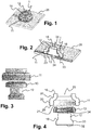
- the illustrated first exemplary embodiment of a battery bridge 1 has an essentially weldable, hollow cylindrical cap (first contact element) 11 and a weldable, essentially cylindrical punch (second contact element) 12. Furthermore, a ring 13 (insulator) is provided, which is arranged between the cap 11 and the punch 12. The punch 12 and the ring 13 are arranged within the through opening 15 of the cap 11. The ring 13 effects a concentric positioning of the punch 12 and the cap 11 in relation to one another in such a way that an air gap 18 is formed between them.
- the air gap has a width of about 50 ⁇ m, for example.
- the illustrated first (open) state of the battery bridge, the metallic cap 11 and the metallic stamp 12 are electrically isolated from one another by means of the electrically insulating ring 13 and the air gap 18.
- the stamp 12 has the same height as the cap 11, so that the upper end face 16 of the cap 11 and the upper end face 34 of the stamp 12 are flush with one another.
- the stamp 12 has a beveled section 19 in which the diameter of the stamp 12 changes from a smaller diameter to a larger diameter.
- the change in diameter is, for example, in the range between 100 ⁇ m and 500 ⁇ m.
- a transition area or "kink" is, as it were, formed in the punch 12, which, as in FIG Fig. 8 shown, laser light of a laser beam 40, which is used for welding, from an underlying electrical circuit - here in the form of a circuit board 25 - shields.
- the cap 11 can also have a beveled section 20 and the ring 13 can have a beveled section 21, this section 21 on the ring 13, such as Fig. 4 shows, is arranged in the region of the top of the ring 13. This results from the arrangement of the ring 13 within the cap 11.
- the cardiac pacemaker 400 has a housing 401 that is hermetically sealed from the outside and a header 402 with a socket 403 for establishing the electrically conductive connection with electrodes (not shown).
- the electrical connection of contacts in the socket with the printed circuit board (PCB) 25 arranged in the housing 401 and an IC (integrated circuit) 409 is made by means of a bushing 405 arranged between the header 402 and the housing 401, which is also hermetically sealed to the outside is.
- PCB printed circuit board
- the IC 409 has electrically conductive connections to a battery 415, a dump resistor 416 and a capacitor unit 417 with a number of capacitors, the battery 415, the dump resistor 416 and the capacitor unit 417 being arranged in the housing 401 of the pacemaker 400.
- battery bridge 1 and test points 420 are arranged in parallel on circuit board 25 such that the electrical connection between battery 415 and IC 409 is open as long as battery bridge 1 is in the first (open) position. State.
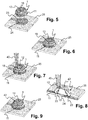
- the battery bridge 1 is produced in that, for example, the cap 11 and the stamp 12 are each produced separately from a metallic material by means of a cold forming or stamping process. Furthermore, the ring 13 is produced, for example, by means of plastic injection molding, for example consisting of POM, PEEK, LCP and / or PBT. Now, first the ring 13 and then the punch 12 are arranged in the through opening 15 of the cap 11 and pressed in so that a press fit is formed between the cap 11 and ring 13 or between ring 13 and punch 12. Through this the ring 13 positions the cap 11 and the punch 12 concentrically to one another and braces them together so that the electrically insulating air gap 18 is formed uniformly. The battery bridge 1 is in the first (open) state.
- a battery bridge 1 produced in this way is now, as in Figures 5 and 6 shown, arranged on a first contact surface 23 or a second contact surface 24 of the circuit board 25 and connected to this in an electrically conductive manner, for example by means of soldering.
- soldering for example, on the cap 11 and / or the punch 12, in each case on the lower end face 29 of the cap 11, in the lower region of the side surface 30 of the cap 11 or on the lower end face 32 of the punch 12 and / or the lower region of the side surface 33 of the stamp 12, a solderable coating (for example containing at least one material from the group comprising gold, ENIG, EPIG, palladium and tin) can be arranged, which was applied before the battery bridge 1 was assembled.
- the first contact surface 23 is electrically conductively connected to the cap 11 and the second contact surface 24 is electrically conductively connected to the stamp 12.
- the circuit is defined via the two test points 420 initialized or started up (power-up).
- the cap 11 and the stamp 12 of the battery bridge 1 can now be fused to one another in a single, automatable work step by means of welding, for example by means of laser welding, without further material supply or removal.
- This step is in the Figures 7 to 9 shown.
- the laser beam 40 is guided along the air gap 18 in the area of the end face 16 of the cap 11 and sets weld points so that the material of the cap 11 and the material of the punch 12 fuse with one another in the area of the air gap 18, an electrically conductive connection between the cap 11 and form die 12 and thereby fill the air gap 18 with a weld 42.
- the path of the electrons from a first conductor track with the first contact surface 23 via the cap 11, the weld seam 42, the punch 12 and the second contact surface 24 of a second conductor track is indicated by arrows 43 in Fig. 11 illustrated.
- the circuit of the circuit board 25 is thus permanently closed and the battery bridge 1 is in the second (closed) state.
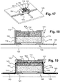
- the height of the cap 11 corresponds to the height of the stamp 12, so that the upper end face 34 of the stamp 12 runs flush with the end face 16 of the cap 11.
- the height of the punch 12 is greater than the height of the cap 11, so that the punch 12 protrudes beyond the end face 16 of the cap.
- the laser beam 40 is somewhat easier to position, since it can be guided along the air gap 18 to the side of the punch 12 (see FIG Fig. 13 ).
- a fillet weld is formed in the area of the air gap 18, which connects the cap 11 to the punch 12 in an electrically conductive manner.
- the inner punch 12 has a smaller height than the outer cap 11.
- the cap has in its end face 16 a through opening 15 through which the laser beam 40 is passed through to establish a connection between the material of the cap 11 and to achieve that of the stamp 12.
- the opening 15 of the cap 11 can also be replaced by a notch, that is to say at least partially closed, with welding then being carried out through the notch in order to realize the electrically conductive connection with the punch 12.
- Fig. 16 shows a fourth embodiment of a battery bridge according to the invention, which the second embodiment according to Figures 12 and 13 resembles.
- the two exemplary embodiments differ only in the form of cap 11, stamp 12 and (not shown) ring 13. While these elements in the second exemplary embodiment according to FIG Figures 12 and 13 are rotationally symmetrical, has the cap 11 of the embodiment according to Fig. 16 a non-rotationally symmetrical shape, namely a Cuboid shape. Accordingly, the punch is also not designed in the shape of a circular cylinder.
- the cross-sectional shape here is essentially an ellipse. Accordingly, the insulator (not shown) is not implemented as a circular ring, but rather as an elliptical / rectangular ring.
- This exemplary embodiment has the advantage that the weld seam runs linearly at least in sections. Other shapes are also conceivable for cap 11, stamp 12 and ring 13 of the battery bridge.
- the battery bridge 101 has a first weldable metallic foil 111 (first contact element) and a second weldable metallic foil 112 (second contact element), which are arranged next to one another, separated by an air gap 118 on a ceramic substrate (insulator) 113.
- the thickness of the metallic foils 111, 112 can be, for example, 400 ⁇ m and the width of the air gap can be, for example, 50 ⁇ m.
- the metallic foils 111, 112 can, for example, have nickel, copper, a copper-nickel alloy and / or stainless steel or consist of one or more of these materials.
- LTCC low temperature cofired ceramic
- HTCC high temperature cofired ceramic with the main component Al 2 O 3
- soldering coating 114 is arranged on the side of the battery bridge 101, which has the first metallic foil 111 and the ceramic substrate 113 on one side and the second metallic foil 112 and the ceramic on the other side -Substrate 113 encloses U-shaped.
- a nickel intermediate layer 115 is arranged between the solder coating 114 and the respective metallic foil 111, 112 or the ceramic substrate 113. An electrically conductive connection from the respective metallic foil 111, 112 to the underside of the ceramic substrate 113 is produced by the solder coating 114 and the nickel intermediate layer 115.
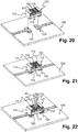
- the method according to the invention for activating an electronic device with a battery bridge 101 according to the invention according to the fifth exemplary embodiment takes place analogously to that based on Figures 5 to 9 explained procedures and is in the Figures 20-23 shown.
- the only difference is that, in the case of the battery bridge 101, the contact elements 111, 112 are not connected directly to the contact surfaces 123, 124 of the circuit board 125, but rather the respective solder coating 114, which makes electrical contact with the first one arranged above the ceramic substrate 113 metallic foil 111 or second metallic foil 112 produces.
- the first metallic foil 111 is also not fused to the second metallic foil 112 along the entire air gap 118, but only two weld points 142 adjacent to one another along the air gap 118 are set. Alternatively, of course, only one welding point or more than two welding points can be provided.
- FIG. 19 The path of the electrons along the conductor track with the first contact surface 123, the solder coating 114, the first metallic foil 111, the weld point 142, the second metallic coating 112, the solder coating 114 and the conductor track with the second contact surface 124 is shown in FIG Fig. 19 indicated by arrows 143.
- a sixth embodiment of a battery bridge 201 is shown.
- This has a first contact element 211, which has an L-shape in cross section, and a second contact element 212, also with an L-shape in cross section.
- These complementary shapes are arranged in such a way that they complement one another and form an air gap 218 between the first contact element 211 and the second contact element 212, namely between the opposing surfaces of these contact elements 211, 212. Accordingly, the air gap 218 forms a step shape.
- an insulator 213 in the form of an adhesive film is arranged, which is, for example, strip-shaped.
- the contact elements 211, 212 are preferably produced by means of cold forming, MIM (metal injection molding), milling or etching, and the insulator 213 is produced from an acrylate adhesive film.
- MIM metal injection molding
- the arrangement on a printed circuit board 225 with a first contact surface 223 and a second contact surface 224 takes place such that the first contact element 211 is soldered directly to the first contact surface 223 and the second contact element 212 is soldered directly to the second contact surface 224.
- a connection of the two contact elements 211, 212 and the second (closed) state of the battery bridge 201 is achieved by two weld points 242.
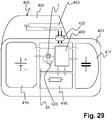
- the seventh exemplary embodiment of a battery bridge 301 according to the invention shown is similar in structure to that in FIG Figures 24 and 25 battery bridge 201 shown.
- the first contact element 311 and the second contact element 312 likewise each have a complementary shape with an L-shaped cross section, between which an air gap 318 is formed.
- the insulator 313, designed for example as an adhesive film, also has a strip shape here in cross section, preferably with a step.
- the battery bridge 301 also has a rectangular ring-shaped housing 316 which surrounds the first contact element 311 and the second contact element 312 in an annular manner.
- first contact element 311 and the second contact element 312 protrude beyond the housing 316 in order to be able to establish proper contact with corresponding contact surfaces of a circuit board.
- the in Fig. 28 The closed state of the battery bridge 311 shown in the figure, the first contact element 311 and the second contact element 312 are connected to one another in an electrically conductive manner via weld points 342.
- the advantages of the above-described SMT-capable battery bridges 1, 101, 201, 301 according to the invention or the above-explained method according to the invention for activating an electronic device lie in particular in the ability to automate the initialization and closing process of the circuit. This enables higher process reliability and a reduction in the throughput time for the power-up to be achieved. It is not necessary to drain material and it is also not necessary to hold down contacts. With a battery bridge 1, 101, 201, 301 that can be welded automatically according to the invention, the production flow can be greatly simplified.
Landscapes
- Engineering & Computer Science (AREA)
- Physics & Mathematics (AREA)
- Optics & Photonics (AREA)
- Mechanical Engineering (AREA)
- Plasma & Fusion (AREA)
- Microelectronics & Electronic Packaging (AREA)
- Manufacturing & Machinery (AREA)
- Health & Medical Sciences (AREA)
- Radiology & Medical Imaging (AREA)
- Veterinary Medicine (AREA)
- Public Health (AREA)
- General Health & Medical Sciences (AREA)
- Animal Behavior & Ethology (AREA)
- Life Sciences & Earth Sciences (AREA)
- Nuclear Medicine, Radiotherapy & Molecular Imaging (AREA)
- Biomedical Technology (AREA)
- Connection Of Batteries Or Terminals (AREA)
Claims (11)
- Elément de liaison pour batterie (1, 101, 201, 301) destiné à un dispositif électronique, de préférence à un implant électronique, comprenant un premier élément de contact (11, 111, 211, 311) électriquement conducteur, un deuxième élément de contact (12, 112, 212, 312) électriquement conducteur et un isolant (13, 113, 213, 313),
où, dans un premier état de l'élément de liaison pour batterie, le premier élément de contact est disposé espacé par rapport au deuxième élément de contact par le biais d'un intervalle d'air (18, 118, 218, 318) prédéfini,
caractérisé en ce que
le premier élément de contact est isolé électriquement par rapport au deuxième élément de contact par l'intervalle d'air et l'isolant,
où le premier élément de contact et le deuxième élément de contact présentent un matériau soudable, où l'élément de liaison pour batterie est conçu de telle façon qu'il puisse être transposé dans un deuxième état au moyen du soudage conjoint du premier élément de contact avec le deuxième élément de contact, état dans lequel l'intervalle d'air entre le premier élément de contact et le deuxième élément de contact est fermé au moins par endroits en étant électriquement conducteur. - Elément de liaison pour batterie (1) selon la revendication 1, caractérisé en ce que l'isolant (13) est conçu dans l'ensemble de forme annulaire, le premier élément de contact (11) est conçu dans l'ensemble en forme de U ou en forme de cylindre creux dans la section transversale et le deuxième élément de contact (12) est conçu dans l'ensemble en forme de cylindre, où l'isolant de forme annulaire est disposé entre le premier élément de contact et le deuxième élément de contact.
- Elément de liaison pour batterie (1) selon la revendication 2, caractérisé en ce que le deuxième élément de contact (12) est disposé à l'intérieur d'un orifice (15) du premier élément de contact (11) se situant à l'intérieur, lequel va de préférence de part en part.
- Elément de liaison pour batterie (1) selon l'une des revendications 2 et 3, caractérisé en ce que le deuxième élément de contact présente un segment (19) biseauté, lequel abrite une lumière laser employée pour le soudage d'un circuit (25) électrique disposé en-dessous de l'élément de liaison pour batterie.
- Elément de liaison pour batterie (1) selon l'une des revendications 2 à 4, caractérisé en ce que le premier élément de contact (11) et/ou le deuxième élément de contact (2) présentent un revêtement améliorant la soudabilité dans un segment servant à la liaison avec le circuit (25) électrique.
- Elément de liaison pour batterie (1) selon l'une des revendications 2 à 5, caractérisé en ce que le deuxième élément de contact (12), dans la région d'une surface frontale supérieure (16) du premier élément de contact (11), dépasse au-dessus de cette surface frontale supérieure sur laquelle a lieu le soudage.
- Elément de liaison pour batterie (1) selon la revendication 1, caractérisé en ce que l'isolant est conçu sous forme de substrat en céramique (113), ainsi que le premier élément de contact est conçu sous forme d'un premier film (111) métallique et le deuxième élément de contact est conçu sous forme de deuxième film (112) métallique, où le premier élément de contact et le deuxième élément de contact sont disposés sur l'isolant sur une distance correspondant à la largeur de l'intervalle d'air (118).
- Elément de liaison pour batterie (1) selon la revendication 1, caractérisé en ce que le premier élément de contact (211, 311) présente une première forme et le deuxième élément de contact (212, 312) présente une deuxième forme, laquelle est complémentaire à la première forme, où l'intervalle d'air (218, 318) est conçu sur les surfaces de la première forme et de la deuxième forme se situant en face et est rempli dans une zone partielle par l'isolant qui est par exemple conçu sous forme d'un film d'adhésif.
- Elément de liaison pour batterie (1) selon l'une des revendications précédentes, caractérisé en ce que l'intervalle d'air (18, 118, 218, 318) présente une largeur dans la plage de 10 µm à 100 µm, de préférence, dans la plage de 30 µm à 80 µm.
- Procédé d'activation d'un dispositif (400) électronique, de préférence, d'un implant électronique, avec un circuit électrique, au moyen d'un élément de liaison pour batterie (1, 101, 201, 301) selon l'une des revendications précédentes, caractérisé par les étapes suivantes :- le positionnement et la fixation de l'élément de liaison pour batterie dans un premier état sur le circuit électrique (25, 125, 225), ainsi que l'établissement d'une liaison électriquement conductrice entre le premier élément de contact (11, 111, 211, 311) et une première piste conductrice ainsi qu'entre le deuxième élément de contact (12, 112, 212, 312) et une deuxième piste conductrice du circuit électrique,- la connexion du circuit électrique avec une source de tension (415) et/ou un condensateur (417), et/ou une résistance de décharge (416),- le démarrage du circuit électrique par le biais d'au moins deux points de test (420),- la transposition de l'élément de liaison pour batterie dans le deuxième état par un soudage conjoint au moins par endroits du premier élément de contact et du deuxième élément de contact de telle manière que l'intervalle d'air (18, 118, 218, 318) est fermé en étant électriquement conducteur au moins par endroits.
- Procédé selon la revendication 10, caractérisé en ce qu'un procédé de soudage en bout à bout ou un procédé de soudage d'angle, ou un procédé de soudage à cœur est mis en œuvre pour le soudage.
Applications Claiming Priority (1)
| Application Number | Priority Date | Filing Date | Title |
|---|---|---|---|
| DE102016101620.9A DE102016101620A1 (de) | 2016-01-29 | 2016-01-29 | Batteriebrücke und Verfahren zum Aktivieren einer elektronischen Vorrichtung |
Publications (2)
| Publication Number | Publication Date |
|---|---|
| EP3200568A1 EP3200568A1 (fr) | 2017-08-02 |
| EP3200568B1 true EP3200568B1 (fr) | 2021-01-06 |
Family
ID=57944259
Family Applications (1)
| Application Number | Title | Priority Date | Filing Date |
|---|---|---|---|
| EP17151706.3A Active EP3200568B1 (fr) | 2016-01-29 | 2017-01-17 | Élément de liaison pour batterie et procédé d'activation d'un dispositif électronique |
Country Status (3)
| Country | Link |
|---|---|
| US (1) | US10615523B2 (fr) |
| EP (1) | EP3200568B1 (fr) |
| DE (1) | DE102016101620A1 (fr) |
Families Citing this family (1)
| Publication number | Priority date | Publication date | Assignee | Title |
|---|---|---|---|---|
| CN106658996A (zh) * | 2016-12-19 | 2017-05-10 | 奇酷互联网络科技(深圳)有限公司 | 实现电路通断切换的方法和印刷电路板 |
Family Cites Families (12)
| Publication number | Priority date | Publication date | Assignee | Title |
|---|---|---|---|---|
| US3766308A (en) | 1972-05-25 | 1973-10-16 | Microsystems Int Ltd | Joining conductive elements on microelectronic devices |
| US4990741A (en) * | 1990-02-06 | 1991-02-05 | Rockwell International Corporation | Method of laser welding |
| NL1001453C2 (nl) | 1995-10-20 | 1997-04-22 | Witmetaal B V | Soldeerelement. |
| US6740821B1 (en) | 2002-03-01 | 2004-05-25 | Micron Technology, Inc. | Selectively configurable circuit board |
| DE10261073A1 (de) * | 2002-12-24 | 2004-07-08 | Rolls-Royce Deutschland Ltd & Co Kg | Verfahren zum Fügen von Werkstücken aus Titanaluminid mittels eines Lötverfahrens |
| US7544220B2 (en) * | 2005-03-31 | 2009-06-09 | Medtronic, Inc. | Welding methods and apparatus for batteries |
| JP2008010501A (ja) | 2006-06-27 | 2008-01-17 | Mitsumi Electric Co Ltd | 回路基板装置 |
| US7968817B2 (en) * | 2006-10-11 | 2011-06-28 | Greatbatch Ltd. | Laser weld process for seam welded electrochemical devices |
| DE102007008549A1 (de) | 2007-02-21 | 2008-08-28 | Siemens Ag | Elektrisches Gerät mit einer eine Anschlussstelle für einen elektrischen Anschlussleiter aufweisenden Leiterbahn und Verfahren zum Verbinden eines elektrischen Anschlussleiters mit einem solchen elektrischen Gerät |
| KR101182235B1 (ko) * | 2009-12-14 | 2012-09-12 | 삼성디스플레이 주식회사 | 증착용 마스크, 그의 제조 방법 및 제조 장치 |
| CN102958274A (zh) | 2011-08-24 | 2013-03-06 | 鸿富锦精密工业(深圳)有限公司 | 电路板 |
| DE102013108563A1 (de) | 2013-08-08 | 2015-02-12 | Thyssenkrupp Steel Europe Ag | Verfahren und Vorrichtung zum Widerstandsschweißen von Sandwichblechen |
-
2016
- 2016-01-29 DE DE102016101620.9A patent/DE102016101620A1/de not_active Withdrawn
-
2017
- 2017-01-05 US US15/399,317 patent/US10615523B2/en active Active
- 2017-01-17 EP EP17151706.3A patent/EP3200568B1/fr active Active
Non-Patent Citations (1)
| Title |
|---|
| None * |
Also Published As
| Publication number | Publication date |
|---|---|
| US10615523B2 (en) | 2020-04-07 |
| DE102016101620A1 (de) | 2017-08-03 |
| US20170222338A1 (en) | 2017-08-03 |
| EP3200568A1 (fr) | 2017-08-02 |
Similar Documents
| Publication | Publication Date | Title |
|---|---|---|
| DE3134557C2 (fr) | ||
| DE10059373B4 (de) | Lecktestgeeignete, kapazitiv gefilterte Durchführung für ein implantierbares medizinisches Gerät | |
| DE69729719T2 (de) | Gefilterte Durchführung für implantierbare medizinische Geräte und entsprechendes Herstellungsverfahren | |
| EP1897588B1 (fr) | Conducteurs tranversants | |
| DE19735409C2 (de) | Verbindungseinrichtung | |
| DE19605252B4 (de) | Oberflächenmontierbare elektrische Mikrominiatur-Schmelzsicherung | |
| DE2366284C2 (de) | Verfahren zum Verschließen eines Halbleiterbauelementgehäuses | |
| EP2329860A1 (fr) | Boîtier de raccordement et sa fabrication | |
| DE102008003659A1 (de) | Schmelzsicherung zur Unterbrechung eines spannungs- und/oder stromführenden Leiters im thermischen Fehlerfall und Verfahren zur Herstellung der Schmelzsicherung | |
| DE2414790C3 (de) | Kristall-Oszillator und Verfahren zu seiner Herstellung | |
| DE102016105696A1 (de) | Elektrolytkondensator | |
| DE102016106482A1 (de) | Verbindungselement für eine elektronische Bauelementanordnung und Verfahren zum Herstellen desselben, elektronische Bauelementanordnung und Verfahren zum Herstellen desselben | |
| DE19523977A1 (de) | Microchip-Sicherung | |
| DE2925509A1 (de) | Packung fuer schaltungselemente | |
| EP3200568B1 (fr) | Élément de liaison pour batterie et procédé d'activation d'un dispositif électronique | |
| DE102008031633B4 (de) | Anordnung zum Befestigen eines elektrischen Bauelements auf einem Träger | |
| DE19739495A1 (de) | Piezoelektrisches Bauteil und Verfahren zur Herstellung desselben | |
| EP1654744B1 (fr) | Module de condensateur et procede de fabrication | |
| EP1606982B1 (fr) | Procede de connexion electrique et mecanique de deux cartes a circuits imprimes | |
| DE3018846A1 (de) | Elektronisches bauelement in chipform und verfahren zur herstellung desselben | |
| EP0418555B1 (fr) | Procédé de fabrication d'un condensateur à électrolyte solide sous forme de chip | |
| EP3069760A1 (fr) | Dispositif electromedical implantable | |
| EP0071917A1 (fr) | Dispositif électrique, groupement de dispositifs ou circuit intégré dont la partie active est placée sur un support métallique et procédé pour la fabrication du dispositif | |
| DE102019129971A1 (de) | Verfahren zum Auflöten eines Bauelements auf eine Leiterplatte, Elektronikeinheit und Feldgerät der Automatisierungstechnik | |
| DE8716967U1 (de) | Flachsicherung für elektrische oder elektronische Schaltkreise |
Legal Events
| Date | Code | Title | Description |
|---|---|---|---|
| PUAI | Public reference made under article 153(3) epc to a published international application that has entered the european phase |
Free format text: ORIGINAL CODE: 0009012 |
|
| STAA | Information on the status of an ep patent application or granted ep patent |
Free format text: STATUS: THE APPLICATION HAS BEEN PUBLISHED |
|
| AK | Designated contracting states |
Kind code of ref document: A1 Designated state(s): AL AT BE BG CH CY CZ DE DK EE ES FI FR GB GR HR HU IE IS IT LI LT LU LV MC MK MT NL NO PL PT RO RS SE SI SK SM TR |
|
| AX | Request for extension of the european patent |
Extension state: BA ME |
|
| STAA | Information on the status of an ep patent application or granted ep patent |
Free format text: STATUS: REQUEST FOR EXAMINATION WAS MADE |
|
| 17P | Request for examination filed |
Effective date: 20180131 |
|
| RBV | Designated contracting states (corrected) |
Designated state(s): AL AT BE BG CH CY CZ DE DK EE ES FI FR GB GR HR HU IE IS IT LI LT LU LV MC MK MT NL NO PL PT RO RS SE SI SK SM TR |
|
| RIC1 | Information provided on ipc code assigned before grant |
Ipc: B23K 101/36 20060101ALN20200616BHEP Ipc: B23K 101/38 20060101ALN20200616BHEP Ipc: H01R 4/02 20060101ALI20200616BHEP Ipc: H01R 43/02 20060101ALI20200616BHEP Ipc: H05K 1/02 20060101AFI20200616BHEP Ipc: B23K 26/32 20140101ALI20200616BHEP Ipc: H05K 3/22 20060101ALN20200616BHEP Ipc: B23K 26/22 20060101ALI20200616BHEP Ipc: H05K 3/32 20060101ALI20200616BHEP Ipc: B23K 26/28 20140101ALI20200616BHEP Ipc: H05K 3/40 20060101ALN20200616BHEP |
|
| GRAP | Despatch of communication of intention to grant a patent |
Free format text: ORIGINAL CODE: EPIDOSNIGR1 |
|
| STAA | Information on the status of an ep patent application or granted ep patent |
Free format text: STATUS: GRANT OF PATENT IS INTENDED |
|
| INTG | Intention to grant announced |
Effective date: 20200730 |
|
| GRAS | Grant fee paid |
Free format text: ORIGINAL CODE: EPIDOSNIGR3 |
|
| GRAA | (expected) grant |
Free format text: ORIGINAL CODE: 0009210 |
|
| STAA | Information on the status of an ep patent application or granted ep patent |
Free format text: STATUS: THE PATENT HAS BEEN GRANTED |
|
| AK | Designated contracting states |
Kind code of ref document: B1 Designated state(s): AL AT BE BG CH CY CZ DE DK EE ES FI FR GB GR HR HU IE IS IT LI LT LU LV MC MK MT NL NO PL PT RO RS SE SI SK SM TR |
|
| REG | Reference to a national code |
Ref country code: GB Ref legal event code: FG4D Free format text: NOT ENGLISH |
|
| REG | Reference to a national code |
Ref country code: AT Ref legal event code: REF Ref document number: 1353777 Country of ref document: AT Kind code of ref document: T Effective date: 20210115 Ref country code: CH Ref legal event code: EP |
|
| REG | Reference to a national code |
Ref country code: DE Ref legal event code: R096 Ref document number: 502017008907 Country of ref document: DE |
|
| REG | Reference to a national code |
Ref country code: IE Ref legal event code: FG4D Free format text: LANGUAGE OF EP DOCUMENT: GERMAN |
|
| REG | Reference to a national code |
Ref country code: NL Ref legal event code: MP Effective date: 20210106 |
|
| REG | Reference to a national code |
Ref country code: LT Ref legal event code: MG9D |
|
| PG25 | Lapsed in a contracting state [announced via postgrant information from national office to epo] |
Ref country code: BG Free format text: LAPSE BECAUSE OF FAILURE TO SUBMIT A TRANSLATION OF THE DESCRIPTION OR TO PAY THE FEE WITHIN THE PRESCRIBED TIME-LIMIT Effective date: 20210406 Ref country code: LT Free format text: LAPSE BECAUSE OF FAILURE TO SUBMIT A TRANSLATION OF THE DESCRIPTION OR TO PAY THE FEE WITHIN THE PRESCRIBED TIME-LIMIT Effective date: 20210106 Ref country code: HR Free format text: LAPSE BECAUSE OF FAILURE TO SUBMIT A TRANSLATION OF THE DESCRIPTION OR TO PAY THE FEE WITHIN THE PRESCRIBED TIME-LIMIT Effective date: 20210106 Ref country code: FI Free format text: LAPSE BECAUSE OF FAILURE TO SUBMIT A TRANSLATION OF THE DESCRIPTION OR TO PAY THE FEE WITHIN THE PRESCRIBED TIME-LIMIT Effective date: 20210106 Ref country code: GR Free format text: LAPSE BECAUSE OF FAILURE TO SUBMIT A TRANSLATION OF THE DESCRIPTION OR TO PAY THE FEE WITHIN THE PRESCRIBED TIME-LIMIT Effective date: 20210407 Ref country code: PT Free format text: LAPSE BECAUSE OF FAILURE TO SUBMIT A TRANSLATION OF THE DESCRIPTION OR TO PAY THE FEE WITHIN THE PRESCRIBED TIME-LIMIT Effective date: 20210506 Ref country code: NO Free format text: LAPSE BECAUSE OF FAILURE TO SUBMIT A TRANSLATION OF THE DESCRIPTION OR TO PAY THE FEE WITHIN THE PRESCRIBED TIME-LIMIT Effective date: 20210406 |
|
| PG25 | Lapsed in a contracting state [announced via postgrant information from national office to epo] |
Ref country code: PL Free format text: LAPSE BECAUSE OF FAILURE TO SUBMIT A TRANSLATION OF THE DESCRIPTION OR TO PAY THE FEE WITHIN THE PRESCRIBED TIME-LIMIT Effective date: 20210106 Ref country code: LV Free format text: LAPSE BECAUSE OF FAILURE TO SUBMIT A TRANSLATION OF THE DESCRIPTION OR TO PAY THE FEE WITHIN THE PRESCRIBED TIME-LIMIT Effective date: 20210106 Ref country code: RS Free format text: LAPSE BECAUSE OF FAILURE TO SUBMIT A TRANSLATION OF THE DESCRIPTION OR TO PAY THE FEE WITHIN THE PRESCRIBED TIME-LIMIT Effective date: 20210106 Ref country code: SE Free format text: LAPSE BECAUSE OF FAILURE TO SUBMIT A TRANSLATION OF THE DESCRIPTION OR TO PAY THE FEE WITHIN THE PRESCRIBED TIME-LIMIT Effective date: 20210106 |
|
| PG25 | Lapsed in a contracting state [announced via postgrant information from national office to epo] |
Ref country code: LU Free format text: LAPSE BECAUSE OF NON-PAYMENT OF DUE FEES Effective date: 20210117 Ref country code: IS Free format text: LAPSE BECAUSE OF FAILURE TO SUBMIT A TRANSLATION OF THE DESCRIPTION OR TO PAY THE FEE WITHIN THE PRESCRIBED TIME-LIMIT Effective date: 20210506 |
|
| REG | Reference to a national code |
Ref country code: BE Ref legal event code: MM Effective date: 20210131 |
|
| REG | Reference to a national code |
Ref country code: DE Ref legal event code: R097 Ref document number: 502017008907 Country of ref document: DE |
|
| PG25 | Lapsed in a contracting state [announced via postgrant information from national office to epo] |
Ref country code: SM Free format text: LAPSE BECAUSE OF FAILURE TO SUBMIT A TRANSLATION OF THE DESCRIPTION OR TO PAY THE FEE WITHIN THE PRESCRIBED TIME-LIMIT Effective date: 20210106 Ref country code: EE Free format text: LAPSE BECAUSE OF FAILURE TO SUBMIT A TRANSLATION OF THE DESCRIPTION OR TO PAY THE FEE WITHIN THE PRESCRIBED TIME-LIMIT Effective date: 20210106 Ref country code: CZ Free format text: LAPSE BECAUSE OF FAILURE TO SUBMIT A TRANSLATION OF THE DESCRIPTION OR TO PAY THE FEE WITHIN THE PRESCRIBED TIME-LIMIT Effective date: 20210106 Ref country code: MC Free format text: LAPSE BECAUSE OF FAILURE TO SUBMIT A TRANSLATION OF THE DESCRIPTION OR TO PAY THE FEE WITHIN THE PRESCRIBED TIME-LIMIT Effective date: 20210106 |
|
| PLBE | No opposition filed within time limit |
Free format text: ORIGINAL CODE: 0009261 |
|
| STAA | Information on the status of an ep patent application or granted ep patent |
Free format text: STATUS: NO OPPOSITION FILED WITHIN TIME LIMIT |
|
| PG25 | Lapsed in a contracting state [announced via postgrant information from national office to epo] |
Ref country code: SK Free format text: LAPSE BECAUSE OF FAILURE TO SUBMIT A TRANSLATION OF THE DESCRIPTION OR TO PAY THE FEE WITHIN THE PRESCRIBED TIME-LIMIT Effective date: 20210106 Ref country code: RO Free format text: LAPSE BECAUSE OF FAILURE TO SUBMIT A TRANSLATION OF THE DESCRIPTION OR TO PAY THE FEE WITHIN THE PRESCRIBED TIME-LIMIT Effective date: 20210106 Ref country code: DK Free format text: LAPSE BECAUSE OF FAILURE TO SUBMIT A TRANSLATION OF THE DESCRIPTION OR TO PAY THE FEE WITHIN THE PRESCRIBED TIME-LIMIT Effective date: 20210106 |
|
| 26N | No opposition filed |
Effective date: 20211007 |
|
| GBPC | Gb: european patent ceased through non-payment of renewal fee |
Effective date: 20210406 |
|
| PG25 | Lapsed in a contracting state [announced via postgrant information from national office to epo] |
Ref country code: AL Free format text: LAPSE BECAUSE OF FAILURE TO SUBMIT A TRANSLATION OF THE DESCRIPTION OR TO PAY THE FEE WITHIN THE PRESCRIBED TIME-LIMIT Effective date: 20210106 Ref country code: ES Free format text: LAPSE BECAUSE OF FAILURE TO SUBMIT A TRANSLATION OF THE DESCRIPTION OR TO PAY THE FEE WITHIN THE PRESCRIBED TIME-LIMIT Effective date: 20210106 Ref country code: GB Free format text: LAPSE BECAUSE OF NON-PAYMENT OF DUE FEES Effective date: 20210406 Ref country code: FR Free format text: LAPSE BECAUSE OF NON-PAYMENT OF DUE FEES Effective date: 20210306 |
|
| PG25 | Lapsed in a contracting state [announced via postgrant information from national office to epo] |
Ref country code: SI Free format text: LAPSE BECAUSE OF FAILURE TO SUBMIT A TRANSLATION OF THE DESCRIPTION OR TO PAY THE FEE WITHIN THE PRESCRIBED TIME-LIMIT Effective date: 20210106 |
|
| PG25 | Lapsed in a contracting state [announced via postgrant information from national office to epo] |
Ref country code: IT Free format text: LAPSE BECAUSE OF FAILURE TO SUBMIT A TRANSLATION OF THE DESCRIPTION OR TO PAY THE FEE WITHIN THE PRESCRIBED TIME-LIMIT Effective date: 20210106 |
|
| PG25 | Lapsed in a contracting state [announced via postgrant information from national office to epo] |
Ref country code: IS Free format text: LAPSE BECAUSE OF FAILURE TO SUBMIT A TRANSLATION OF THE DESCRIPTION OR TO PAY THE FEE WITHIN THE PRESCRIBED TIME-LIMIT Effective date: 20210506 |
|
| PG25 | Lapsed in a contracting state [announced via postgrant information from national office to epo] |
Ref country code: BE Free format text: LAPSE BECAUSE OF NON-PAYMENT OF DUE FEES Effective date: 20210131 |
|
| REG | Reference to a national code |
Ref country code: AT Ref legal event code: MM01 Ref document number: 1353777 Country of ref document: AT Kind code of ref document: T Effective date: 20220117 |
|
| PG25 | Lapsed in a contracting state [announced via postgrant information from national office to epo] |
Ref country code: AT Free format text: LAPSE BECAUSE OF NON-PAYMENT OF DUE FEES Effective date: 20220117 |
|
| PG25 | Lapsed in a contracting state [announced via postgrant information from national office to epo] |
Ref country code: HU Free format text: LAPSE BECAUSE OF FAILURE TO SUBMIT A TRANSLATION OF THE DESCRIPTION OR TO PAY THE FEE WITHIN THE PRESCRIBED TIME-LIMIT; INVALID AB INITIO Effective date: 20170117 |
|
| PG25 | Lapsed in a contracting state [announced via postgrant information from national office to epo] |
Ref country code: NL Free format text: LAPSE BECAUSE OF NON-PAYMENT OF DUE FEES Effective date: 20210206 Ref country code: CY Free format text: LAPSE BECAUSE OF FAILURE TO SUBMIT A TRANSLATION OF THE DESCRIPTION OR TO PAY THE FEE WITHIN THE PRESCRIBED TIME-LIMIT Effective date: 20210106 |
|
| P01 | Opt-out of the competence of the unified patent court (upc) registered |
Effective date: 20230615 |
|
| PGFP | Annual fee paid to national office [announced via postgrant information from national office to epo] |
Ref country code: IE Payment date: 20240118 Year of fee payment: 8 |
|
| PG25 | Lapsed in a contracting state [announced via postgrant information from national office to epo] |
Ref country code: MK Free format text: LAPSE BECAUSE OF FAILURE TO SUBMIT A TRANSLATION OF THE DESCRIPTION OR TO PAY THE FEE WITHIN THE PRESCRIBED TIME-LIMIT Effective date: 20210106 |
|
| PGFP | Annual fee paid to national office [announced via postgrant information from national office to epo] |
Ref country code: DE Payment date: 20240119 Year of fee payment: 8 Ref country code: CH Payment date: 20240202 Year of fee payment: 8 |
|
| PG25 | Lapsed in a contracting state [announced via postgrant information from national office to epo] |
Ref country code: MT Free format text: LAPSE BECAUSE OF FAILURE TO SUBMIT A TRANSLATION OF THE DESCRIPTION OR TO PAY THE FEE WITHIN THE PRESCRIBED TIME-LIMIT Effective date: 20210106 |
|
| REG | Reference to a national code |
Ref country code: DE Ref legal event code: R119 Ref document number: 502017008907 Country of ref document: DE |
|
| REG | Reference to a national code |
Ref country code: CH Ref legal event code: PL |
|
| PG25 | Lapsed in a contracting state [announced via postgrant information from national office to epo] |
Ref country code: DE Free format text: LAPSE BECAUSE OF NON-PAYMENT OF DUE FEES Effective date: 20250801 |
|
| PG25 | Lapsed in a contracting state [announced via postgrant information from national office to epo] |
Ref country code: CH Free format text: LAPSE BECAUSE OF NON-PAYMENT OF DUE FEES Effective date: 20250131 |
|
| PG25 | Lapsed in a contracting state [announced via postgrant information from national office to epo] |
Ref country code: TR Free format text: LAPSE BECAUSE OF FAILURE TO SUBMIT A TRANSLATION OF THE DESCRIPTION OR TO PAY THE FEE WITHIN THE PRESCRIBED TIME-LIMIT Effective date: 20210106 |
|
| PG25 | Lapsed in a contracting state [announced via postgrant information from national office to epo] |
Ref country code: IE Free format text: LAPSE BECAUSE OF NON-PAYMENT OF DUE FEES Effective date: 20250117 |