EP3201832B1 - Fingerprint or palmprint sensor - Google Patents
Fingerprint or palmprint sensor Download PDFInfo
- Publication number
- EP3201832B1 EP3201832B1 EP15788117.8A EP15788117A EP3201832B1 EP 3201832 B1 EP3201832 B1 EP 3201832B1 EP 15788117 A EP15788117 A EP 15788117A EP 3201832 B1 EP3201832 B1 EP 3201832B1
- Authority
- EP
- European Patent Office
- Prior art keywords
- sensor
- cell
- node
- cells
- acquisition
- Prior art date
- Legal status (The legal status is an assumption and is not a legal conclusion. Google has not performed a legal analysis and makes no representation as to the accuracy of the status listed.)
- Not-in-force
Links
Images

Classifications
-
- G—PHYSICS
- G06—COMPUTING OR CALCULATING; COUNTING
- G06V—IMAGE OR VIDEO RECOGNITION OR UNDERSTANDING
- G06V40/00—Recognition of biometric, human-related or animal-related patterns in image or video data
- G06V40/10—Human or animal bodies, e.g. vehicle occupants or pedestrians; Body parts, e.g. hands
- G06V40/12—Fingerprints or palmprints
- G06V40/13—Sensors therefor
- G06V40/1306—Sensors therefor non-optical, e.g. ultrasonic or capacitive sensing
-
- A—HUMAN NECESSITIES
- A61—MEDICAL OR VETERINARY SCIENCE; HYGIENE
- A61B—DIAGNOSIS; SURGERY; IDENTIFICATION
- A61B5/00—Measuring for diagnostic purposes; Identification of persons
- A61B5/117—Identification of persons
- A61B5/1171—Identification of persons based on the shapes or appearances of their bodies or parts thereof
- A61B5/1172—Identification of persons based on the shapes or appearances of their bodies or parts thereof using fingerprinting
-
- G—PHYSICS
- G06—COMPUTING OR CALCULATING; COUNTING
- G06V—IMAGE OR VIDEO RECOGNITION OR UNDERSTANDING
- G06V40/00—Recognition of biometric, human-related or animal-related patterns in image or video data
- G06V40/10—Human or animal bodies, e.g. vehicle occupants or pedestrians; Body parts, e.g. hands
- G06V40/12—Fingerprints or palmprints
- G06V40/13—Sensors therefor
- G06V40/1318—Sensors therefor using electro-optical elements or layers, e.g. electroluminescent sensing
-
- G—PHYSICS
- G06—COMPUTING OR CALCULATING; COUNTING
- G06V—IMAGE OR VIDEO RECOGNITION OR UNDERSTANDING
- G06V40/00—Recognition of biometric, human-related or animal-related patterns in image or video data
- G06V40/10—Human or animal bodies, e.g. vehicle occupants or pedestrians; Body parts, e.g. hands
- G06V40/12—Fingerprints or palmprints
- G06V40/13—Sensors therefor
- G06V40/1329—Protecting the fingerprint sensor against damage caused by the finger
-
- G—PHYSICS
- G06—COMPUTING OR CALCULATING; COUNTING
- G06V—IMAGE OR VIDEO RECOGNITION OR UNDERSTANDING
- G06V40/00—Recognition of biometric, human-related or animal-related patterns in image or video data
- G06V40/10—Human or animal bodies, e.g. vehicle occupants or pedestrians; Body parts, e.g. hands
- G06V40/12—Fingerprints or palmprints
- G06V40/1365—Matching; Classification
-
- G—PHYSICS
- G06—COMPUTING OR CALCULATING; COUNTING
- G06V—IMAGE OR VIDEO RECOGNITION OR UNDERSTANDING
- G06V40/00—Recognition of biometric, human-related or animal-related patterns in image or video data
- G06V40/10—Human or animal bodies, e.g. vehicle occupants or pedestrians; Body parts, e.g. hands
- G06V40/12—Fingerprints or palmprints
- G06V40/1382—Detecting the live character of the finger, i.e. distinguishing from a fake or cadaver finger
- G06V40/1394—Detecting the live character of the finger, i.e. distinguishing from a fake or cadaver finger using acquisition arrangements
-
- H—ELECTRICITY
- H03—ELECTRONIC CIRCUITRY
- H03K—PULSE TECHNIQUE
- H03K17/00—Electronic switching or gating, i.e. not by contact-making and –breaking
- H03K17/94—Electronic switching or gating, i.e. not by contact-making and –breaking characterised by the way in which the control signals are generated
- H03K17/96—Touch switches
- H03K17/962—Capacitive touch switches
-
- H—ELECTRICITY
- H04—ELECTRIC COMMUNICATION TECHNIQUE
- H04N—PICTORIAL COMMUNICATION, e.g. TELEVISION
- H04N25/00—Circuitry of solid-state image sensors [SSIS]; Control thereof
- H04N25/70—SSIS architectures; Circuits associated therewith
- H04N25/76—Addressed sensors, e.g. MOS or CMOS sensors
- H04N25/77—Pixel circuitry, e.g. memories, A/D converters, pixel amplifiers, shared circuits or shared components
Definitions
- the present application relates to the field of fingerprint or palmar sensors.
- sensors have been proposed to perform an electronic acquisition of a fingerprint and / or palmar, that is to say to provide an image of the pattern formed by the ridges and hollows of the skin of a finger, several fingers, and / or the palm of the hand.
- optical sensors, capacitive sensors, thermal sensors, ultrasonic sensors, and electric field sensors have been proposed.
- Such sensors are disclosed in the documents WO2014 / 091093 or JP2006343229 .
- TFT Thin Film Transistor
- a support substrate one or several elementary acquisition cells, each elementary cell (or pixel) comprising an acquisition element, for example photoelectric, pyroelectric or capacitive, and one or more TFT transistors for controlling this element.
- transistor TFT we mean here, transistors formed by successive deposits of conductive, insulating and semiconductive layers on the support substrate.
- the semiconductor channel-forming region of the transistor is produced by depositing a layer of a semiconductor material, for example hydrogenated amorphous silicon or polycrystalline silicon (polycrystalline rendering after annealing, for example).
- this deposit may be preceded by a deposit of a conductive layer for forming a gate electrode, source or drain of the transistor.
- IGZO of the "Indium Gallium Zinc Oxide” - indium gallium zinc oxide
- This deposit may be preceded by a deposit of a conductive layer for forming a gate electrode, source or drain of the transistor.
- the impression sensors made in TFT technology have the advantage of being relatively inexpensive, in particular by virtue of the use of a support substrate made of a low-cost material such as glass (instead of a substrate made of monocrystalline silicon generally used to make transistors), and to be easily integrated in many types of electronic devices, and in particular in devices already using TFT technology to perform other functions, for example to make screens of display.
- TFT technology is particularly advantageous in the field of fingerprint sensors in which the surface of the sensor is substantially identical to the surface of the impression to be acquired, that is to say in which no optical focusing system (or objective) is placed between the sensor and the object whose image is to be acquired. Indeed, because of their large sizes, the realization of such sensors in and on silicon substrates would be a cost far too high for most applications.
- One embodiment provides a fingerprint or palm sensor comprising: on a support substrate, a plurality of elementary acquisition cells, made of TFT technology, each cell comprising a photodetector and a pyroelectric conversion element connected to the same capacitive reading node of the cell, and a read circuit connecting the capacitive read node of the cell to a conductive output track of the cell a source bright lighting; and a heat source distinct from the light source.
- the support substrate is transparent.
- the photodetector and the pyroelectric conversion element are connected in parallel.
- the senor comprises a circuit adapted to control the acquisition of a thermal image and the acquisition of an optical image by the cells of the sensor, this circuit being adapted, during the entire acquisition phase of the optical image, to turn on the light source and keep the heat source off, and, during the entire acquisition phase of the thermal image, to keep the light source off.
- the senor comprises a circuit adapted to control the acquisition of a thermal image and the acquisition of an optical image by the cells of the sensor, this circuit being adapted to implement the acquisition of thermal image during part of an integration period of the acquisition phase of the optical image during which the light source is turned on.
- the photodetector and the pyroelectric conversion element are connected to a capacitive read node of the cell.
- each cell the photodetector and the pyroelectric conversion element are connected to an intermediate node of the cell, the intermediate node being connected to the capacitive reading node of the cell by a selection transistor, and each cell further comprising: a reference capacitor connected between the read capacitive node and an application node of a control signal; and an electrode connected to the capacitive readout node, the electrode being coated with a dielectric layer and being adapted to form a capacitance with the skin of a user for capacitive acquisition of a fingerprint image.
- the photodetector and the pyroelectric conversion element are connected to a same selection transistor allowing, in the open state, to isolate the photodetector from the pyroelectric element.
- the cells are arrayed in rows and columns, and the heat source is controllable to heat the cells line by line.
- the cells are voltage-read cells, each cell comprising: a reset transistor connecting the read capacitive node to an application node of a reset potential and a read circuit of each cell comprising a follower source-mounted transistor, whose gate is connected to the read node, and whose source is connected to an output track of the cell via a read transistor.
- the cells are load-reading cells, the read circuit of each cell comprising a read transistor connecting the read node to an output track of the cell.
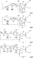
- the figure 1 is an electrical diagram illustrating an example of an optical TFT fingerprint sensor 100.
- the sensor 100 comprises a plurality of identical or similar elementary acquisition cells 101 made in TFT technology on one side of a transparent support substrate, for example made of glass, which will be hereinafter conventionally referred to as the upper face of the substrate.
- a single cell 101 has been represented on the figure 1 .
- Each cell 101 comprises a photodetector PS, for example a photodiode whose anode is connected to an application node of a reference potential GND (for example ground), and whose cathode is connected to a capacitive read node. SN of the cell.
- GND for example ground
- the photodetector PS is a PIN type photodiode, or an organic photodiode.
- the capacity of the reading node SN has been represented in dashed lines in the form of a capacitor whose one electrode is connected to the node SN and whose other electrode is connected to the node GND.
- the capacity of the node SN may be a parasitic capacitance of another element of the cell, for example the parasitic capacitance of the photodiode PS (to which is added the parasitic capacitance of the transistor RS in the example represented), or a specific ability.
- the capacity of the SN node will not be represented in the following figures.
- Each cell 101 further comprises a read transistor RS connecting its read node SN to a conductive output track CL of the cell.
- the control gate of the transistor RS is connected to a VG RS node for applying a control potential of this transistor.
- the output track CL of the cell 101 is connected to an output stage 103 of the sensor.
- the output stage 103 comprises an operational amplifier 105 including an inverting input (-) connected to the track CL and a non-inverting input (+) connected to a node V pol of application of a potential of polarization.
- the output stage 103 further comprises an analog-to-digital converter 107 (ADC) whose input is connected to the output of the amplifier 105.
- the output stage further comprises a capacitor 109 in parallel with a control switch 111 between the inverting input (-) and the output of the amplifier 105.
- the sensor 100 further comprises a lighting light source, not shown.
- the light source is disposed on the side of the face of the substrate opposite to the cells 101, which will be hereinafter called conventionally the underside of the substrate.
- the operation of the sensor 100 is as follows.
- the user places one finger (or more) on or above the top surface of the sensor (cell side 101).
- the backlight light source disposed on the side of the substrate opposite the cells, illuminates the finger through transparent areas of the assembly formed by the support substrate and the cells 101.
- the light is then backscattered by the finger towards the photodiodes PS, with, at each cell 101, a more or less attenuation depending on whether the finger portion above the cell corresponds to a peak or a hollow of the skin of the finger.
- the light source can be placed above or next to the finger, the light then being transmitted by the finger towards the PS photodiodes of the sensor, with a greater or lesser attenuation depending on the portion of finger located above the cell corresponds to a ridge or hollow of the skin of the finger.
- the substrate may be non-transparent.
- the photogenerated charges are transferred to the output track CL of the cell (which may have been previously reset by closing the switch 111) via the transistor RS, and the signal resulting is read by the output stage 103 connected to the track CL.
- the RS transistor being bidirectional, it also resets the PS photodiode to a fixed potential before the start of a new integration period.
- the cells 101 may be connected to the same output track CL and share a same output stage 103 of the sensor.
- the cells 101 are for example arranged in a matrix according to rows and columns, the cells of one and the same column being connected to the same output track CL and to the same output stage 103, and the cells of distinct columns being connected to each other.
- the cells 101 are controllable simultaneously line by line, that is to say that the cells 101 of the same line have their nodes VG RS connected to the same control track and the cells 101 of lines distinct have their VG RS nodes connected to separate control tracks.
- the figure 2 is an electrical diagram illustrating an example of a thermal TFT fingerprint sensor 120.
- the sensor 120 of the figure 2 includes common elements with the sensor 100 of the figure 1 . These elements will not be described again.
- the sensor 120 differs from the sensor 100 mainly in that, in the sensor 120, elementary acquisition cells 121 of thermal type replace the elementary optical acquisition cells 101 of the sensor 100.
- the elementary cells 121 of the sensor of the figure 2 differ from the elementary cells 101 of the sensor of the figure 1 in that, in each cell 121, a pyroelectric conversion element PYR, connecting the reading node SN of the cell to the node GND, replaces the photodetector PS of the cells 101.
- the pyroelectric conversion element PYR typically comprises a layer of a pyroelectric material such as aluminum nitride (AlN), zinc oxide (ZnO), a polymer such as polyvinylidene fluoride (PVDF), whose pyroelectric coefficient is of the order of 40 ⁇ C / m 2 / K, a ceramic material of the PZT (lead titanozirconate) type, whose pyroelectric coefficient is of the order of 350 ⁇ C / m 2 / K, or a crystalline material of the TGS (Triglycine) type sulfate) or LiTaO 3 , arranged between two conductive layers respectively connected to the node SN and to the node GND.
- a pyroelectric material such as aluminum nitride (AlN), zinc oxide (ZnO), a polymer such as polyvinylidene fluoride (PVDF), whose pyroelectric coefficient is of the order of 40 ⁇ C
- the sensor 120 further differs from the sensor 100 of the figure 1 in that it does not include a backlight light source, but includes a heat source, not shown.
- the heat source may comprise a network of resistors regularly distributed over the surface of the sensor.
- the heat source comprises a resistance elementary cell, this resistance being disposed in the vicinity of the pyroelectric element of the cell.
- the resistors of the heat source are preferably arranged on the same side of the support substrate as the cells 101, that is to say on the side of the upper face of the substrate.
- the operation of the sensor 120 is as follows.
- the user has placed one finger (or more) on or above the top surface of the sensor (cell side 121).
- the heat source of the sensor is then turned on, and heats the pyroelectric conversion elements PYR which consequently generate electrical charges on the reading nodes SN of the corresponding cells 121.
- the amount of heat received by each pyroelectric conversion element PYR when the heat source is turned on is greater when the corresponding cell is surmounted by a hollow of the skin, than when it is surmounted by a ridge. Indeed, when the cell is surmounted by a ridge, the skin absorbs a larger part of the heat emitted by the source than when the cell is surmounted by a hollow.
- the amount of electric charges generated on its reading node SN is greater than when the cell is surmounted by a peak.
- the charges accumulated on the node SN are transferred to the output track CL of the cell via the transistor RS , and the resulting signal is read by the output stage 103 connected to the track CL. Since the RS transistor is bidirectional, it also resets the SN node before the start of a new integration period.
- the heat source is controlled to produce a heat pulse, and the cells are read a certain time after the start of the pulse, and / or shortly after the end of this pulse , so as to overcome the phenomena of thermalization causing, over time, the standardization of the accumulated charge levels on the reading nodes SN of the different cells.
- the cells 121 may be connected to the same output track CL and share a same output stage 103 of the sensor.
- the cells 121 are, for example, arranged in a matrix according to rows and columns, the cells of one and the same column being connected to the same output track CL and to the same output stage 103, and the cells of distinct columns being connected to separate output tracks CL and separate output stages 103.
- the cells 121 are controllable simultaneously line by line.
- the heat source is then controllable to heat cells 121 line by line. This makes it possible to scan the sensor line by line by synchronizing the ignition of the heat source with the reading of the cells, and thus to minimize the effects of the thermalization on the acquired image.
- the heat source may consist of conductive tracks extending along the lines of the sensor, for example metal tracks (for example in molybdenum or aluminum), tracks in a metal oxide, possibly transparent (eg indium tin oxide), polycrystalline silicon tracks, or conductive polymer tracks.
- metal tracks for example in molybdenum or aluminum
- tracks in a metal oxide possibly transparent (eg indium tin oxide), polycrystalline silicon tracks, or conductive polymer tracks.
- the elementary acquisition cells 101 and 121 are load-reading cells, that is to say that the reading of a cell passes through the transfer, on the output track CL of the cell (via the RS read transistor of the cell), accumulated charges on the read node SN of the cell.
- An advantage of the load-reading acquisition cells is that they are particularly simple and / or compact (a single transistor per cell in the examples of FIGS. Figures 1 and 2 ).
- Such cells are particularly suitable for TFT technologies, for example based on amorphous silicon or indium gallium zinc oxide, in which the transistors are relatively bulky.
- the pitch of the pixels can typically be of the order of 20 to 50 ⁇ m, which limits the number of transistors that can include each cell.
- the figure 3 is an electrical diagram illustrating another example of an optical or thermal TFT fingerprint sensor 130.
- the sensor 130 of the figure 3 includes elements common to the sensors 100 and 120 of the Figures 1 and 2 . These elements will not be described again.
- the sensor 130 of the figure 3 differs from sensors 100 or 120 of Figures 1 and 2 essentially in that, in the sensor 130, elementary acquisition cells 131 with a voltage reading replace the load-reading cells 101 or 121 of the sensors 100 or 120.
- the sensor 130 also differs from the sensors 100 and 120 in this respect. that in the sensor 130, one or more output stages 133 replace the output stage (s) 103 of the sensors 100 or 120.
- each acquisition elementary cell 131 comprises a connected photoelectric or pyroelectric conversion element 132 between a capacitive read node SN of the cell and an application node of a reference potential GND of the cell.
- the conversion element 132 is an optical conversion element PS of the type described in relation to the figure 1 or a PYR thermal conversion element of the type described in connection with the figure 2 .
- Each cell 131 further comprises a reset transistor RT connecting its read node SN to an application node of a reset potential V RT , for example a positive potential with respect to the potential of the GND node.
- Each cell 131 further comprises a follower source transistor SF, the gate of which is connected to the node SN, and a read transistor RD connecting the source of the transistor SF to the output track CL of the cell.
- the drain of the transistor SF is connected to an application node of a reference potential, for example the potential V RT or another potential.
- the control gate of the transistor RT is connected to a node VG RT for applying a control potential of this transistor
- the gate of the transistor RD is connected to a node VG RD for applying a control potential of this transistor.
- the output track CL of the cell 131 is connected to an output stage 133 of the sensor.
- the output stage 133 comprises an amplifier 135 whose input is connected to the track CL and whose output is connected to an analog-to-digital converter 107 (ADC).
- ADC analog-to-digital converter
- the amplifier 135 is optional, and may in particular be omitted if the potential level of the track CL is compatible with the input of the analog-digital converter 107.
- the sensor 130 further comprises a lighting light source (not shown) if the elements 132 are optical acquisition elements, or a heat source (not shown) if the elements 132 are pyroelectric acquisition elements.
- the conversion element 132 of the cell is first reset via the transistor RT of the cell.
- the transistor RT is then turned off, and during an integration period, photogenerated charges or charges generated by the pyroelectric effect accumulate on the read node SN of the cell.
- the potential of the reading node SN is transferred to the output track CL of the cell via the transistors SF and RD.
- the transistor RD of the cell is turned on.
- the potential of the output track CL is then read by the output stage 133 associated with the output track CL.
- An advantage of the voltage read acquisition cells is that they provide a better signal-to-noise ratio than the load-reading cells of the type described in connection with the Figures 1 and 2 .
- the figure 4 is an electrical diagram illustrating an example of a capacitive TFT fingerprint sensor 140.
- the sensor 140 is a voltage reading sensor.
- the sensor 140 comprises elements that are common with the sensor 130 of the figure 3 . These elements will not be described again below.
- the sensor 140 differs from the sensor 130 of the figure 3 essentially in that, in the sensor 140, capacitive type elementary acquisition cells 141 replace the optical or thermal acquisition cells 131 of the sensor 130.
- the sensor 140 does not include a light source of illumination nor heat source.
- Each cell 141 comprises the same elements as a cell 131 of the sensor of the figure 3 except for the optical or pyroelectric conversion element 132.
- Each cell 141 further comprises a reference capacitor C REF , connected between the read node SN of the cell and a signal application CMD node. control.
- Each cell 141 further comprises a conductive electrode EL connected to the node SN, the electrode EL being coated with a dielectric layer and being intended to form a capacitance with the skin of a finger of the user.
- the electrode EL is preferably placed in the vicinity of the upper surface of the sensor, so that the dielectric thickness between the upper surface of the sensor (intended to receive the finger of the user) and the electrode EL does not exceed a few microns, for example 10 microns.
- the operation of the sensor 140 is as follows.
- the user places a finger (or more) on or above the top surface of the sensor (EL electrode side).
- the read node SN of the cell is first reset via the transistor RT of the cell.
- the transistor RT is then turned off, then a control signal, for example a square-wave or step voltage, is applied to the control node CMD of the cell.
- the reference capacitance C REF and the capacitance formed between the electrode EL and the skin of the finger form a capacitive divider bridge.
- a potential depending on the capacitance formed between the electrode EL and the skin is then established on the reading node SN of the cell.
- the value of this potential is different depending on whether the EL electrode is surmounted by a peak or a hollow of the user's skin.
- the potential of the node SN is transferred to the output track CL of the cell via the transistors SF and RD. For this, the transistor RD of the cell is turned on.
- the potential of the output track CL is then read by the output stage 133 associated with the output track CL.
- the step applied on the CMD node can then be reduced to its initial value.
- a fingerprint sensor made in TFT technology, this sensor comprising, on a transparent insulating support substrate, for example glass, a plurality of elementary acquisition cells, each cell comprising a photodetector, a pyroelectric conversion element, and at least one TFT transistor.
- a transparent insulating support substrate for example glass
- a plurality of elementary acquisition cells each cell comprising a photodetector, a pyroelectric conversion element, and at least one TFT transistor.
- it is planned to combine, in each elementary cell, an optical acquisition element and a thermal acquisition element, so that the sensor provides, during the acquisition of a fingerprint or palmar, an optical image and a thermal image of the impression.
- An advantage of such a sensor is that the two images are acquired by means of acquisition elements based on phenomena having, a priori, no physical relationship. Indeed, the photodetector generates electric charges when it receives photons, and the pyroelectric element generates electric charges when its temperature varies.
- the inventors have indeed found that, generally, an imprint difficult to acquire in the optical field is easier to acquire in the thermal field, and conversely, a footprint difficult to acquire in the thermal field is easier to acquire in the field optical.
- the fact of integrating the photodetector and the pyroelectric conversion element in the same elementary cell makes it possible to share TFT transistors for controlling the cell between the photodetector and the pyroelectric conversion element, and thus to limit the bulk, the complexity and cost of the sensor.
- a same TFT transistor of the cell is connected to both the photodetector and the pyroelectric conversion element, which makes it possible to limit the space requirement.
- the photoelectric and pyroelectric conversion elements are connected in parallel, which makes it possible to obtain particularly simple and compact elementary cells.
- the figure 5 is an example of an optical and thermal TFT fingerprint sensor 150.
- the sensor 150 of the figure 5 is a voltage reading sensor.
- the sensor 150 of the figure 5 includes common elements with the sensor 130 of the figure 3 . These elements will not be described again.
- the sensor 150 of the figure 5 differs from the sensor 130 of the figure 3 essentially in that, in the sensor 150, elementary acquisition cells 151, both optical and thermal, replace the optical or thermal cells 131 of the sensor 130.
- each elementary acquisition cell 151 comprises the same elements as an elementary acquisition cell of the sensor 130, with the exception of the conversion element 132.
- Each cell 151 further comprises a photodetector PS, for example of the type described in connection with the figure 1 , in series with a selection transistor SW1 between the capacitive read node SN of the cell and the reference node GND of the cell.
- the photodetector PS is a photodiode whose anode is connected to the GND node and whose cathode is connected to the node SN via the transistor SW1.
- Each cell 151 further comprises a pyroelectric conversion element PYR, for example of the type described in connection with the figure 2 in series with a selection transistor SW2 between the read node SN of the cell and the node GND.
- the pyroelectric element PYR has a first electrode connected to the GND node and a second electrode connected to the node SN via the transistor SW2.
- the gate of the transistor SW1 is connected to a node VG SW1 for applying a control signal of this transistor
- the gate of the transistor SW2 is connected to a node VG SW2 for applying a control signal of this transistor .
- the sensor 150 further comprises an illumination light source (not shown) for carrying out an optical acquisition of an image, and a heat source (not shown), distinct from the light source, for the implementation of a thermal acquisition of an image.
- the cells 151 may be arranged in a matrix according to rows and columns, the cells of the same line being controlled simultaneously and the cells of distinct lines being controlled successively.
- the heat source can be controllable to heat cells 151 line by line.
- the transistors SW1 and SW2 make it possible to isolate the photodetector PS and / or the pyroelectric element PYR from the reading node SN.
- Two images, respectively optical and thermal, can therefore be successively acquired by the sensor.
- the transistors SW1 are in the on state and the transistors SW2 are non-conducting.
- the transistors SW2 are in the on state, and the transistors SW1 are in the off state.
- the sensor can be controlled identically or similarly to what has been described in connection with the figure 3 .
- the reset transistor RT, and the SF and RD transistors of the read stage are shared by the two PS and PYR conversion elements.
- the example of figure 5 can be adapted to realize an optical and thermal sensor to read in charges, by replacing, in the sensor of the figure 1 , the photodetector PS by the set formed, in the example of the figure 5 by the transistors SW1 and SW2, the photodetector PS, and the pyroelectric element PYR.
- a disadvantage of the sensor 150 lies in the additional cost and the size associated with the presence, in each elementary acquisition cell, of the two selection transistors SW1 and SW2.
- the figure 6 is an electrical diagram illustrating an example of an optical and thermal TFT fingerprint sensor 160 according to a first embodiment.
- the sensor 160 of the figure 6 is a voltage reading sensor. This sensor comprises elements common with the sensor 150 of the figure 5 . These elements will not be described again.
- the sensor 160 of the figure 6 differs from the sensor 150 of the figure 5 essentially in that, in the sensor 160, elementary acquisition cells 161, both optical and thermal, replace the optical and thermal cells 151 of the sensor 150.
- the cells 161 of the sensor 160 differ from the cells 151 of the sensor 150 by they do not include the transistors SW1 and SW2 of the cells 151.
- the photodetector PS (and more particularly the cathode node of the photodiode PS in the example shown) is connected to the node SN , and the pyroelectric element PYR is connected to the node SN.
- the photodetector PS and the pyroelectric element PYR are connected in parallel between the node SN and the node GND.
- the photodetector PS and the pyroelectric element PYR are directly connected to the node SN, and therefore to the transistors RT and SF of the cell.
- the sensor 160 further comprises a light source of illumination (not shown) intended for the implementation of an optical acquisition of an image, and a heat source (not shown) intended for the implementation of a thermal acquisition of an image.
- the light source and the heat source are for example controllable, through a control circuit not shown, for, during a fingerprint acquisition phase, to be alternately switched on and off.
- the light source can be extinguished, and the heat source switched on.
- the pyroelectric element PYR is capable of generating electrical charges representative of the pattern of the print to be acquired.
- the light source can be lit and the heat source extinguished.
- only the photodetector PS is capable of generating electrical charges representative of the pattern of the print to be acquired.
- the sensor 160 can be controlled in the same way or similar to what has been described in connection with the figure 3 .
- reset potential levels applied for optical acquisition and for thermal acquisition are not necessarily the same.
- different reset levels can be provided to balance the levels of the output signals, and to optimize the use of an analog-to-digital converter.
- the readings of the optical signal and the thermal signal can be readings of the two correlated sample type (generally referred to in the art as CDS), in which the output value is equal to the difference between a Useful signal level and a reset level read on the CL track.
- CDS two correlated sample type
- a read of the reset level can be performed, via the track CL, after each reset of the read node SN.
- the heat source when acquiring the thermal image, can be turned on before the end of the reset phase of the read node (i.e., before opening the reset RT), in order to overcome any possible parasitic noise related to current transient effects by the heat source.
- the light source can be lit before the end of the reset phase of the reading node, in order to overcome any possible parasitic noise related to transient current-pulling effects by the light source.
- the acquisition of a thermal image point by the pyroelectric element PYR is much faster than the acquisition of an optical image point by the photodetector PS .
- the reading on the node SN of a potential representative of the imprint pattern is performed 10 to 500 ⁇ s after the ignition of the heat source (in particular to overcome any contrast degradation related to the thermalization), and, during an acquisition of an optical image, the integration time of the photodetector is between 10 and 50 ms.
- the thermal acquisition can be performed during the optical integration period, which reduces the total time required for the acquisition of optical and thermal images.
- the thermal acquisition is preferably performed at the beginning of the optical integration period, for example in the first half of the optical integration period, or at least 500 ⁇ s before the end of the integration period. optical, to ensure that the charges generated by the pyroelectric element on the node SN during the thermal acquisition have time to cancel by effect thermalization before the end of the optical integration period.
- An advantage of the sensor 160 of the figure 6 resides in the low number of transistors per elementary cell 161 with respect to the sensor of the figure 5 .
- the dimensions (surfaces and / or thicknesses) of the photodetector PS and the pyroelectric element PYR, the power of the backlighting light source, the integration time of the photodetector, and the power of the source of heat are chosen so that the voltage levels generated on the node SN during an optical acquisition and during a thermal acquisition are of the same order of magnitude, or at least remain in both cases in a range of acceptable voltage levels for the output stage.
- the above parameters are chosen so that, for the same type of skin structure (peak or trough) above an elementary cell, the voltage level generated on the node SN during an optical acquisition is between 0.5 and 2 times the voltage level generated on the SN node during a thermal acquisition.
- the figure 7 is an electrical diagram illustrating another example of an optical and thermal TFT fingerprint sensor 170 according to the first embodiment.
- the sensor 170 of the figure 7 is a load-bearing sensor. This sensor comprises elements common to the sensors 100 and 120 of the Figures 1 and 2 . These elements will not be described again.
- the sensor 170 of the figure 7 differs from sensors 100 and 120 of Figures 1 and 2 essentially in that, in the sensor 170, elementary acquisition cells 171, both optical and thermal, replace the optical cells 101 or thermal cells 121 of the sensors 100 and 120.
- the cells 171 of the sensor 170 differ from the cells 101 or Sensors 100 and 120 in that they comprise a photodetector PS and a pyroelectric element PYR connected in parallel between the SN and GND nodes of the cell.
- the RS read transistor of the cell is directly connected to both the photodetector PS and the pyroelectric element PYR.
- the transistor RS is shared by the photodetector PS and the pyroelectric element
- the sensor 170 further comprises, as in the example of the figure 6 , a light source of illumination (not shown) intended for carrying out an optical acquisition of an image, and a heat source (not shown) intended for carrying out a thermal acquisition of a picture.
- the light source and the heat source are for example controllable via a control circuit not shown, in the same way or similar to that described in connection with the figure 6 .
- the operation of the sensor 170 is identical or similar to what has been described in connection with the figure 6 , at with the difference that, in the sensor 170, the elementary acquisition cells are load-reading cells. In particular, the cell resets are performed through their RS read transistors.
- the dimensions (surfaces and / or thicknesses) of the photodetector PS and of the pyroelectric element PYR, the power of the backlighting light source, the integration time of the photodetector, and the power of the heat source are preferably chosen so that the amounts of charges generated on the node SN during an optical acquisition and during a thermal acquisition are of the same order of magnitude.
- the figure 8 is an electrical diagram illustrating another example of an optical and thermal TFT fingerprint sensor 180 according to the first embodiment, this sensor further comprising capacitive type acquisition means.
- the sensor 180 of the figure 8 is a voltage reading sensor. This sensor comprises elements that are common with the sensor 160 of the figure 6 . These elements will not be described again.
- the sensor 180 of the figure 8 differs from the sensor 160 of the figure 6 essentially in that, in the sensor 180, elementary acquisition cells 181 replace the cells 161 of the sensor 160.
- the cells 181 of the sensor differ from the cells 161 of the sensor 180 in that they comprise means for acquiring data.
- capacitive type imprint for example of the type described in connection with the figure 4 .
- each cell 181 comprises a selection transistor SW connecting the read node SN of the cell to the photodetector PS and to the pyroelectric element PYR. More particularly, in each cell 181, the photodetector PS and the pyroelectric element PYR are connected in parallel between the node GND and an intermediate node n1, and the selection transistor SW is connected between the node n1 and the node SN.
- the photodetector PS is a photodiode whose anode is connected to the GND node and whose cathode is connected to the node n1.
- the gate of the selection transistor SW is connected to a node VG SW of application of a control signal of this transistor.
- each cell 181 comprises a reference capacitor C REF connected between the reading node SN of the cell and a CMD for applying a control signal, and a conducting electrode EL connected to the node SN, the EL electrode being coated with a dielectric layer and being intended to form a capacitance with the skin of a finger of the user.
- the transistor RT may be connected between the nodes V RT and n1.
- the transistor SW makes it possible to isolate the capacitive acquisition stage from the optical and pyroelectric acquisition stage. This makes it possible in particular, during the implementation of a capacitive acquisition, that the capacitances of the photodetector PS and the pyroelectric element PYR do not contribute to increasing the capacity of the reading node SN, which would make it difficult to acquire a capacitive type imprint signal on the SN node.
- three images of the same fingerprint, respectively optical, thermal and capacitive, can be acquired by the sensor.
- the reset transistor RT, and the SF and RD transistors of the read stage, are shared by the three capacitive, photoelectric, and pyroelectric conversion elements.
- the transistors SW of the cells 181 can be set to the off state, and the cells can be controlled in a manner similar to or identical to that described in connection with the figure 4 .
- the transistors SW of the cells 181 can be turned on, and the cells can be controlled in a manner similar to or identical to that described in connection with the figure 6 .
- the capacity of the elements PYR and PS is generally relatively large compared to the capacity of the node SN (and in particular the capacitance C REF ).
- the thermal and optical signals are not significantly altered by the capacity of the SN node when the transistor SW is in the on state.
- the integration of the light by the photodetector PS can be performed in part or in full during the capacitive reading, which reduces the total time of acquisition of the imprint.
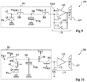
- the figure 9 is an electrical diagram illustrating an example of an optical and thermal TFT fingerprint sensor 190 according to a second embodiment.
- the sensor 190 of the figure 9 is a load-bearing sensor. This sensor comprises elements common with the sensor 170 of the figure 7 . These elements will not be described again.
- the sensor 190 of the figure 9 differs from the sensor 170 of the figure 7 essentially in that, in the sensor 190, elementary acquisition cells 191 replace the cells 171 of the sensor 170.
- the cells 191 of the sensor 190 differ from the cells 171 of the sensor 170 in that, in the cells 191, the photodetector PS is not connected directly between the nodes GND and SN, but is connected between the node GND and an intermediate node n2, the node n2 being connected to the node SN by a selection transistor SW.
- the pyroelectric element PYR is connected directly to the node SN. More particularly, in this example, the photodetector PS is a photodiode whose anode is connected to the GND node and whose cathode is connected to the node n2.
- the selection transistor SW is connected to both the photodetector PS and the pyroelectric element PYR.
- the read transistor RS of the cell is shared by the photodetector PS and the pyroelectric element PYR.
- the transistors SW make it possible, in each elementary acquisition cell, to isolate the photodetector PS from the rest of the cell.
- the figure 10 is an electrical diagram illustrating another example of an optical and thermal TFT fingerprint sensor 200 according to the second embodiment.
- the sensor 200 of the figure 10 is a voltage reading sensor. This sensor comprises elements that are common with the sensor 160 of the figure 6 . These elements will not be described again.
- the sensor 200 of the figure 10 differs from the sensor 160 of the figure 6 essentially in that, in the sensor 200, elementary acquisition cells 201 replace the cells 161 of the sensor 160.
- the cells 201 of the sensor 200 differ from the cells 161 of the sensor 160 in that, in the cells 201, the PS photodetector is not connected directly between the nodes GND and SN, but is connected between the node GND and an intermediate node n3, the node n3 being connected to the node SN by a selection transistor SW.
- the pyroelectric element PYR is connected directly to the node SN. More particularly, in this example, the photodetector PS is a photodiode whose anode is connected to the GND node and whose cathode is connected to the node n3.
- the selection transistor SW is connected to both the photodetector PS and the pyroelectric element PYR.
- the transistors RT, SF and RD of the cell are shared by the photodetector PS and the pyroelectric element PYR.
- the transistors SW make it possible, in each elementary acquisition cell, to isolate the photodetector PS from the rest of the cell, which offers additional control possibilities with respect to the sensor 160 of the figure 6 , all limiting the cost and bulk compared to a sensor with two selection transistors SW1 and SW2 per cell, of the type described in connection with the figure 5 .
- this gives more flexibility in the dimensioning of PS and thermal conversion elements PYR, than in a sensor of the type described in connection with the figure 6 .
- the photodetector PS and the pyroelectric element PYR can be interchanged, that is to say that the PYR element can be placed behind the selection transistor SW, between the node n2 or n3 and the node GND, the photodetector PS being then directly connected to the SN node.
- This choice can be made according to the respective values of the capacities of the PYR and PS elements.
- the photodetector can generate, in addition to the useful signal representative of the pattern of the print to be acquired, noise associated in particular with the currents of darkness and / or light. room.
- the source of light so as to acquire an image representative of the noise generated by the photodetector PS (particularly related to dark currents and parasitic ambient light). Once this image is acquired, it can be subtracted from the final optical image, and, if the photodetector is not isolated from the pyroelectric element, to the final thermal image.
- thermal and optical instead of performing two separate readings, thermal and optical, respectively, seeking to distinguish the thermal signal from the optical signal, as described above, it is possible to read the sum of the photogenerated charges and charges generated by the pyroelectric element, without seeking to separate them, in order to acquire an image combining the optical signal and the thermal signal, which can prove useful for acquiring certain difficult footprints.
- control method in which, during the acquisition of a print, an optical image and a thermal image are read, may be provided for embodiments in which reads several optical images and / or several thermal images of the same footprint.
- the optical integration period is several times greater than the time required to implement the steps of thermal reading of all lines of the sensor, it can be expected to scan successively several times all sensor to acquire several thermal images, then, at the last scan of the sensor, to acquire the optical image.
- the embodiments described above can be combined with other fingerprint acquisition technologies, for example ultrasonic or electric field acquisition technologies, or technologies in which an RF signal is applied through the skin of the user.
- the temperature variation exploited by the PYR pyroelectric conversion elements is a variation that occurs when the user places his finger on the sensor, and / or removes it from the sensor.
- Such sensors can be of static type (the surface of the sensor is at least equal to the surface of the impression to be acquired, and the finger does not move relative to the sensor during the acquisition) or of scanning type (the surface the sensor is smaller than the area of the impression to be acquired, and the finger scrolls past the sensor during acquisition).
Landscapes
- Engineering & Computer Science (AREA)
- Multimedia (AREA)
- Physics & Mathematics (AREA)
- Human Computer Interaction (AREA)
- General Physics & Mathematics (AREA)
- Theoretical Computer Science (AREA)
- Health & Medical Sciences (AREA)
- Life Sciences & Earth Sciences (AREA)
- Signal Processing (AREA)
- Heart & Thoracic Surgery (AREA)
- Public Health (AREA)
- Biomedical Technology (AREA)
- Biophysics (AREA)
- Medical Informatics (AREA)
- Molecular Biology (AREA)
- Surgery (AREA)
- Animal Behavior & Ethology (AREA)
- General Health & Medical Sciences (AREA)
- Pathology (AREA)
- Veterinary Medicine (AREA)
- Image Input (AREA)
- Solid State Image Pick-Up Elements (AREA)
- Photometry And Measurement Of Optical Pulse Characteristics (AREA)
- Measurement Of The Respiration, Hearing Ability, Form, And Blood Characteristics Of Living Organisms (AREA)
- Facsimile Heads (AREA)
- Transforming Light Signals Into Electric Signals (AREA)
Description
La présente demande de brevet revendique la priorité de la demande de brevet français
La présente demande concerne le domaine des capteurs d'empreintes digitales ou palmaires.The present application relates to the field of fingerprint or palmar sensors.
Divers types de capteurs ont été proposés pour réaliser une acquisition électronique d'une empreinte digitale et/ou palmaire, c'est-à-dire pour fournir une image du motif formé par les crêtes et creux de la peau d'un doigt, de plusieurs doigts, et/ou de la paume de la main. On a notamment proposé des capteurs optiques, des capteurs capacitifs, des capteurs thermiques, des capteurs à ultrasons, et des capteurs à champ électrique. De tels capteurs sont divulgués dans les documents
On s'intéresse ici plus particulièrement aux capteurs d'empreintes réalisés en technologie TFT (de l'anglais "Thin Film Transistor" - transistor en couches minces), c'est-à-dire comportant, sur un substrat de support, une ou plusieurs cellules élémentaires d'acquisition, chaque cellule élémentaire (ou pixel) comportant un élément d'acquisition, par exemple photoélectrique, pyroélectrique ou capacitif, et un ou plusieurs transistors TFT permettant de commander cet élément. Par transistor TFT, on entend ici des transistors formés par dépôts successifs de couches conductrices, isolantes et semiconductrices sur le substrat de support. En particulier, dans un transistor TFT, la région semiconductrice de formation de canal du transistor est réalisée par dépôt d'une couche d'un matériau semiconducteur, par exemple du silicium amorphe hydrogéné, du silicium polycristallin (rendu polycristallin après un recuit par exemple), ou encore un matériau de type IGZO (de l'anglais "Indium Gallium Zinc Oxyde" - oxyde d'indium gallium zinc), ce dépôt pouvant être précédé d'un dépôt d'une couche conductrice servant à former une électrode de grille, de source ou de drain du transistor. Les capteurs d'empreintes réalisés en technologie TFT présentent l'avantage d'être relativement peu onéreux, notamment grâce à l'utilisation d'un substrat de support en un matériau à faible coût tel que le verre (au lieu d'un substrat en silicium monocristallin généralement utilisé pour réaliser des transistors), et d'être facilement intégrables dans de nombreux types de dispositifs électroniques, et en particulier dans des dispositifs utilisant déjà la technologie TFT pour réaliser d'autres fonctions, par exemple pour réaliser des écrans d'affichage. La technologie TFT est tout particulièrement avantageuse dans le domaine des capteurs d'empreintes dans lesquels la surface du capteur est sensiblement identique à la surface de l'empreinte à acquérir, c'est-à-dire dans lesquels aucun système optique de focalisation (ou objectif) n'est placé entre le capteur et l'objet dont on souhaite acquérir une image. En effet, en raison de leurs grandes tailles, la réalisation de tels capteurs dans et sur des substrats de silicium aurait un coût bien trop élevé pour la plupart des applications.Of particular interest here are fingerprint sensors made in TFT (Thin Film Transistor) technology, that is to say comprising, on a support substrate, one or several elementary acquisition cells, each elementary cell (or pixel) comprising an acquisition element, for example photoelectric, pyroelectric or capacitive, and one or more TFT transistors for controlling this element. By transistor TFT, we mean here, transistors formed by successive deposits of conductive, insulating and semiconductive layers on the support substrate. In particular, in a TFT transistor, the semiconductor channel-forming region of the transistor is produced by depositing a layer of a semiconductor material, for example hydrogenated amorphous silicon or polycrystalline silicon (polycrystalline rendering after annealing, for example). or a type of material IGZO (of the "Indium Gallium Zinc Oxide" - indium gallium zinc oxide), this deposit may be preceded by a deposit of a conductive layer for forming a gate electrode, source or drain of the transistor. The impression sensors made in TFT technology have the advantage of being relatively inexpensive, in particular by virtue of the use of a support substrate made of a low-cost material such as glass (instead of a substrate made of monocrystalline silicon generally used to make transistors), and to be easily integrated in many types of electronic devices, and in particular in devices already using TFT technology to perform other functions, for example to make screens of display. TFT technology is particularly advantageous in the field of fingerprint sensors in which the surface of the sensor is substantially identical to the surface of the impression to be acquired, that is to say in which no optical focusing system (or objective) is placed between the sensor and the object whose image is to be acquired. Indeed, because of their large sizes, the realization of such sensors in and on silicon substrates would be a cost far too high for most applications.
Un mode de réalisation prévoit un capteur d'empreintes digitales ou palmaires comportant : sur un substrat de support, une pluralité de cellules élémentaires d'acquisition, réalisées en technologie TFT, chaque cellule comportant un photodétecteur et un élément de conversion pyroélectrique reliés à un même noeud capacitif de lecture de la cellule, et un circuit de lecture reliant le noeud capacitif de lecture de la cellule à une piste conductrice de sortie de la cellule une source lumineuse d'éclairage ; et une source de chaleur distincte de la source lumineuse.One embodiment provides a fingerprint or palm sensor comprising: on a support substrate, a plurality of elementary acquisition cells, made of TFT technology, each cell comprising a photodetector and a pyroelectric conversion element connected to the same capacitive reading node of the cell, and a read circuit connecting the capacitive read node of the cell to a conductive output track of the cell a source bright lighting; and a heat source distinct from the light source.
Selon un mode de réalisation, le substrat de support est transparent.According to one embodiment, the support substrate is transparent.
Selon un mode de réalisation, le photodétecteur et l'élément de conversion pyroélectrique sont connectés en parallèle.According to one embodiment, the photodetector and the pyroelectric conversion element are connected in parallel.
Selon un mode de réalisation, le capteur comporte un circuit adapté à commander l'acquisition d'une image thermique et l'acquisition d'une image optique par les cellules du capteur, ce circuit étant adapté, pendant toute la phase d'acquisition de l'image optique, à allumer la source lumineuse et maintenir la source de chaleur éteinte, et, pendant toute la phase d'acquisition de l'image thermique, à maintenir la source lumineuse éteinte.According to one embodiment, the sensor comprises a circuit adapted to control the acquisition of a thermal image and the acquisition of an optical image by the cells of the sensor, this circuit being adapted, during the entire acquisition phase of the optical image, to turn on the light source and keep the heat source off, and, during the entire acquisition phase of the thermal image, to keep the light source off.
Selon un mode de réalisation, le capteur comporte un circuit adapté à commander l'acquisition d'une image thermique et l'acquisition d'une image optique par les cellules du capteur, ce circuit étant adapté à mettre en oeuvre l'acquisition de l'image thermique pendant une partie d'une période d'intégration de la phase d'acquisition de l'image optique pendant laquelle la source lumineuse est allumée.According to one embodiment, the sensor comprises a circuit adapted to control the acquisition of a thermal image and the acquisition of an optical image by the cells of the sensor, this circuit being adapted to implement the acquisition of thermal image during part of an integration period of the acquisition phase of the optical image during which the light source is turned on.
Selon un mode de réalisation, dans chaque cellule, le photodétecteur et l'élément de conversion pyroélectrique sont connectés au à un noeud capacitif de lecture de la cellule.According to one embodiment, in each cell, the photodetector and the pyroelectric conversion element are connected to a capacitive read node of the cell.
Selon un mode de réalisation, dans chaque cellule, le photodétecteur et l'élément de conversion pyroélectrique sont connectés à un noeud intermédiaire de la cellule, le noeud intermédiaire étant relié au noeud capacitif de lecture de la cellule par un transistor de sélection, et chaque cellule comprenant en outre : un condensateur de référence connecté entre le noeud capacitif de lecture et un noeud d'application d'un signal de commande ; et une électrode connectée au noeud capacitif de lecture, l'électrode étant revêtue d'une couche diélectrique et étant destinée à former une capacité avec la peau d'un utilisateur en vue d'une acquisition capacitive d'une image d'empreinte.According to one embodiment, in each cell, the photodetector and the pyroelectric conversion element are connected to an intermediate node of the cell, the intermediate node being connected to the capacitive reading node of the cell by a selection transistor, and each cell further comprising: a reference capacitor connected between the read capacitive node and an application node of a control signal; and an electrode connected to the capacitive readout node, the electrode being coated with a dielectric layer and being adapted to form a capacitance with the skin of a user for capacitive acquisition of a fingerprint image.
Selon un mode de réalisation, le photodétecteur et l'élément de conversion pyroélectrique sont connectés à un même transistor de sélection permettant, à l'état ouvert, d'isoler le photodétecteur de l'élément pyroélectrique.According to one embodiment, the photodetector and the pyroelectric conversion element are connected to a same selection transistor allowing, in the open state, to isolate the photodetector from the pyroelectric element.
Selon un mode de réalisation, les cellules sont disposées en matrice selon des lignes et des colonnes, et la source de chaleur est commandable pour chauffer les cellules ligne par ligne.In one embodiment, the cells are arrayed in rows and columns, and the heat source is controllable to heat the cells line by line.
Selon un mode de réalisation, les cellules sont des cellules à lecture en tension, chaque cellule comportant : un transistor de réinitialisation reliant le noeud capacitif de lecture à un noeud d'application d'un potentiel de réinitialisation et le un circuit de lecture de chaque cellule comportant un transistor monté en source suiveuse, dont la grille est connectée au noeud de lecture, et dont la source est reliée à une piste de sortie de la cellule par l'intermédiaire d'un transistor de lecture.According to one embodiment, the cells are voltage-read cells, each cell comprising: a reset transistor connecting the read capacitive node to an application node of a reset potential and a read circuit of each cell comprising a follower source-mounted transistor, whose gate is connected to the read node, and whose source is connected to an output track of the cell via a read transistor.
Selon un mode de réalisation, les cellules sont des cellules à lecture en charge, le circuit de lecture de chaque cellule comportant un transistor de lecture reliant le noeud de lecture à une piste de sortie de la cellule.According to one embodiment, the cells are load-reading cells, the read circuit of each cell comprising a read transistor connecting the read node to an output track of the cell.
Ces caractéristiques et leurs avantages, ainsi que d'autres, seront exposés en détail dans la description suivante de modes de réalisation particuliers faite à titre non limitatif en relation avec les figures jointes parmi lesquelles :
- la
figure 1 est un schéma électrique illustrant un exemple d'un capteur d'empreintes TFT optique ; - la
figure 2 est un schéma électrique illustrant un exemple d'un capteur d'empreintes TFT thermique ; - la
figure 3 est un schéma électrique illustrant un autre exemple d'un capteur d'empreintes TFT optique ou thermique ; - la
figure 4 est un schéma électrique illustrant un exemple d'un capteur d'empreintes TFT capacitif ; - la
figure 5 est un schéma électrique illustrant un autre exemple de réalisation d'un capteur d'empreintes TFT ; - la
figure 6 est un schéma électrique illustrant un premier mode de réalisation d'un capteur d'empreintes TFT ; - la
figure 7 est un schéma électrique illustrant une variante de réalisation du capteur de lafigure 6 ; - la
figure 8 est un schéma électrique illustrant une autre variante de réalisation du capteur de lafigure 6 ; - la
figure 9 est un schéma électrique illustrant un deuxième mode de réalisation d'un capteur d'empreintes TFT ; et - la
figure 10 est un schéma électrique illustrant une variante de réalisation du capteur de lafigure 9 .
- the
figure 1 is an electrical diagram illustrating an example of an optical TFT fingerprint sensor; - the
figure 2 is an electrical diagram illustrating an example of a thermal TFT fingerprint sensor; - the
figure 3 is an electrical diagram illustrating another example of an optical or thermal TFT fingerprint sensor; - the
figure 4 is an electrical diagram illustrating an example of a capacitive TFT fingerprint sensor; - the
figure 5 is an electrical diagram illustrating another embodiment of a TFT fingerprint sensor; - the
figure 6 is an electrical diagram illustrating a first embodiment of a TFT fingerprint sensor; - the
figure 7 is an electrical diagram illustrating an embodiment variant of the sensor of thefigure 6 ; - the
figure 8 is an electrical diagram illustrating another variant embodiment of the sensor of thefigure 6 ; - the
figure 9 is an electrical diagram illustrating a second embodiment of a TFT fingerprint sensor; and - the
figure 10 is an electrical diagram illustrating an embodiment variant of the sensor of thefigure 9 .
Par souci de clarté, de mêmes éléments ont été désignés par de mêmes références aux différentes figures. De plus, seuls les éléments utiles à la compréhension des modes de réalisation décrits ont été détaillés. En particulier, les circuits périphériques de commande des cellules élémentaires des capteurs d'empreintes TFT décrits n'ont pas été détaillés, la réalisation de tels circuits étant à la portée de l'homme de l'art à la lecture de la présente description. On notera par ailleurs que dans la présente description, lorsque des architectures de cellules élémentaires, de matrices de cellules élémentaires ou de capteurs d'empreintes sont décrites, on utilise le terme "connecté" pour désigner une liaison électrique directe, sans composant électronique intermédiaire, par exemple au moyen d'une piste conductrice, et le terme "couplé" ou le terme "relié", pour désigner une liaison électrique directe ou via un ou plusieurs composants intermédiaires, par exemple via un transistor.For the sake of clarity, the same elements have been designated with the same references in the various figures. In addition, only the elements useful for understanding the described embodiments have been detailed. In particular, the peripheral control circuits of the elementary cells of the TFT impression sensors described have not been detailed, the realization of such circuits being within the reach of those skilled in the art on reading the present description. Note also that in the present description, when architectures of elementary cells, elementary cell matrices or fingerprint sensors are described, the term "connected" is used to designate a direct electrical connection, without intermediate electronic component, for example by means of a conductive track, and the term "coupled" or the term "connected", to designate a direct electrical connection or via one or more intermediate components, for example via a transistor.
La
Le capteur 100 comprend en outre une source lumineuse d'éclairage, non représentée. A titre d'exemple, la source d'éclairage est disposée du côté de la face du substrat opposée aux cellules 101, que l'on appellera ci-après par convention la face inférieure du substrat.The
Le fonctionnement du capteur 100 est le suivant. L'utilisateur place un doigt (ou plusieurs) sur ou au-dessus de la surface supérieure du capteur (côté cellules 101). La source lumineuse de rétroéclairage, disposée du côté du substrat opposé aux cellules, éclaire le doigt à travers des zones transparentes de l'ensemble formé par le substrat de support et les cellules 101. La lumière est alors rétrodiffusée par le doigt en direction des photodiodes PS, avec, au niveau de chaque cellule 101, une atténuation plus ou moins importante selon que la portion de doigt située au-dessus de la cellule correspond à une crête ou à un creux de la peau du doigt. A titre de variante, la source lumineuse peut être placée au-dessus ou à côté du doigt, la lumière étant alors transmise par le doigt en direction des photodiodes PS du capteur, avec une atténuation plus ou moins importante selon que la portion de doigt située au-dessus de la cellule correspond à une crête ou à un creux de la peau du doigt. Dans ce cas, le substrat peut être non transparent. Pendant une période d'intégration d'une cellule 101, le transistor de lecture RS de la cellule est non passant, et la lumière réfléchie par le doigt est convertie en charges électriques par la photodiode PS de la cellule. Ces charges sont stockées sur le noeud de lecture SN de la cellule. A la fin de la période d'intégration, les charges photogénérées sont transférées sur la piste de sortie CL de la cellule (qui peut avoir été préalablement réinitialisée par fermeture de l'interrupteur 111) par l'intermédiaire du transistor RS, et le signal résultant est lu par l'étage de sortie 103 connecté à la piste CL. Le transistor RS étant bidirectionnel, il permet également de réinitialiser la photodiode PS à un potentiel fixé avant le début d'une nouvelle période d'intégration.The operation of the
A titre d'exemple, plusieurs cellules élémentaires 101 peuvent être connectées à une même piste de sortie CL et partager un même étage de sortie 103 du capteur. Les cellules 101 sont par exemple disposées en matrice selon des lignes et des colonnes, les cellules d'une même colonne étant connectées à une même piste de sortie CL et à un même étage de sortie 103, et les cellules de colonnes distinctes étant connectées à des pistes de sortie CL distinctes et à des étages de sortie 103 distincts. A titre d'exemple, les cellules 101 sont commandables simultanément ligne par ligne, c'est-à-dire que les cellules 101 d'une même ligne ont leurs noeuds VGRS connectés à une même piste de commande et les cellules 101 de lignes distinctes ont leurs noeuds VGRS connectés à des pistes de commande distinctes.By way of example, several
La
Le capteur 120 diffère en outre du capteur 100 de la
Le fonctionnement du capteur 120 est le suivant. L'utilisateur a placé un doigt (ou plusieurs) sur ou au-dessus de la surface supérieure du capteur (côté cellules 121). La source de chaleur du capteur est alors mise en marche, et chauffe les éléments de conversion pyroélectrique PYR qui génèrent en conséquence des charges électriques sur les noeuds de lecture SN des cellules 121 correspondantes. La quantité de chaleur reçue par chaque élément de conversion pyroélectrique PYR lorsque la source de chaleur est allumée est plus importante lorsque la cellule correspondante est surmontée par un creux de la peau, que lorsqu'elle est surmontée par une crête. En effet, lorsque la cellule est surmontée par une crête, la peau absorbe une part plus importante de la chaleur émise par la source que lorsque la cellule est surmontée par un creux. Ainsi, lorsqu'une cellule 121 est surmontée par un creux de la peau, la quantité de charges électriques générées sur son noeud de lecture SN est plus importante que lorsque la cellule est surmontée par une crête. A la fin d'une période d'intégration pendant laquelle le transistor de lecture RS de la cellule est maintenu non passant, les charges accumulées sur le noeud SN sont transférées sur la piste de sortie CL de la cellule par l'intermédiaire du transistor RS, et le signal résultant est lu par l'étage de sortie 103 connecté à la piste CL. Le transistor RS étant bidirectionnel, il permet également de réinitialiser le noeud SN avant le début d'une nouvelle période d'intégration.The operation of the
De préférence, lors d'une acquisition, la source de chaleur est commandée pour produire une impulsion de chaleur, et les cellules sont lues un certain temps après le début de l'impulsion, et/ou peu de temps après la fin de cette impulsion, de façon à s'affranchir des phénomènes de thermalisation entraînant, avec le temps, l'uniformisation des niveaux de charge accumulés sur les noeuds de lecture SN des différentes cellules.Preferably, during an acquisition, the heat source is controlled to produce a heat pulse, and the cells are read a certain time after the start of the pulse, and / or shortly after the end of this pulse , so as to overcome the phenomena of thermalization causing, over time, the standardization of the accumulated charge levels on the reading nodes SN of the different cells.
Comme dans l'exemple de la
Dans les capteurs 100 et 120 des
La
La piste de sortie CL de la cellule 131 est connectée à un étage de sortie 133 du capteur. Dans cet exemple, l'étage de sortie 133 comprend un amplificateur 135 dont une entrée est reliée à la piste CL et dont la sortie est reliée à un convertisseur analogique-numérique 107 (ADC). L'amplificateur 135 est optionnel, et peut notamment être omis si le niveau de potentiel de la piste CL est compatible avec l'entrée du convertisseur analogique-numérique 107.The output track CL of the
Le capteur 130 comprend en outre une source lumineuse d'éclairage (non représentée) si les éléments 132 sont des éléments d'acquisition optique, ou une source de chaleur (non représentée) si les éléments 132 sont des éléments d'acquisition pyroélectriques.The
Le fonctionnement d'une cellule élémentaire 131 du capteur 130 lors d'une phase d'acquisition d'une empreinte va maintenant être décrit. L'élément de conversion 132 de la cellule est d'abord réinitialisé par l'intermédiaire du transistor RT de la cellule. Le transistor RT est ensuite rendu non passant, et, pendant une période d'intégration, des charges photogénérées ou des charges générées par effet pyroélectrique s'accumulent sur le noeud de lecture SN de la cellule. A la fin de l'intégration, le potentiel du noeud de lecture SN est reporté sur la piste de sortie CL de la cellule par l'intermédiaire des transistors SF et RD. Pour cela, le transistor RD de la cellule est rendu passant. Le potentiel de la piste de sortie CL est alors lu par l'étage de sortie 133 associé à la piste de sortie CL.The operation of an
Un avantage des cellules d'acquisition à lecture en tension est qu'elles permettent d'obtenir un meilleur rapport signal sur bruit que les cellules à lecture en charge du type décrit en relation avec les
La
Le fonctionnement du capteur 140 est le suivant. L'utilisateur place un doigt (ou plusieurs) sur ou au-dessus de la surface supérieure du capteur (côté électrodes EL). Lors de l'acquisition d'un point d'image de l'empreinte par une cellule 141, le noeud de lecture SN de la cellule est d'abord réinitialisé par l'intermédiaire du transistor RT de la cellule. Le transistor RT est ensuite rendu non passant, puis un signal de commande, par exemple une tension en créneau ou échelon, est appliqué sur le noeud de commande CMD de la cellule. La capacité de référence CREF et la capacité formée entre l'électrode EL et la peau du doigt forment un pont diviseur capacitif. Un potentiel dépendant de la capacité formée entre l'électrode EL et la peau s'établit alors sur le noeud de lecture SN de la cellule. La valeur de ce potentiel est différente selon que l'électrode EL est surmontée par une crête ou par un creux de la peau de l'utilisateur. Le potentiel du noeud SN est reporté sur la piste de sortie CL de la cellule par l'intermédiaire des transistors SF et RD. Pour cela, le transistor RD de la cellule est rendu passant. Le potentiel de la piste de sortie CL est alors lu par l'étage de sortie 133 associé à la piste de sortie CL. L'échelon appliqué sur le noeud CMD peut alors être ramené à sa valeur initiale.The operation of the
Selon un aspect de modes de réalisation décrits, on prévoit un capteur d'empreintes réalisé en technologie TFT, ce capteur comportant, sur un substrat de support isolant transparent, par exemple en verre, une pluralité de cellules élémentaires d'acquisition, chaque cellule comportant un photodétecteur, un élément de conversion pyroélectrique, et au moins un transistor TFT. En d'autres termes, on prévoit de combiner, dans chaque cellule élémentaire, un élément d'acquisition optique et un élément d'acquisition thermique, de façon que le capteur fournisse, lors de l'acquisition d'une empreinte digitale ou palmaire, une image optique et une image thermique de l'empreinte.According to one aspect of embodiments described, there is provided a fingerprint sensor made in TFT technology, this sensor comprising, on a transparent insulating support substrate, for example glass, a plurality of elementary acquisition cells, each cell comprising a photodetector, a pyroelectric conversion element, and at least one TFT transistor. In other words, it is planned to combine, in each elementary cell, an optical acquisition element and a thermal acquisition element, so that the sensor provides, during the acquisition of a fingerprint or palmar, an optical image and a thermal image of the impression.
Un avantage d'un tel capteur est que les deux images sont acquises au moyen d'éléments d'acquisition basés sur des phénomènes n'ayant, à priori, pas de relation physique. En effet, le photodétecteur génère des charges électriques lorsqu'il reçoit des photons, et l'élément pyroélectrique génère des charges électriques lorsque sa température varie. Ceci permet de résoudre, dans une certaine mesure, les difficultés rencontrées lors de l'acquisition d'empreintes de doigts dits "difficiles", c'est-à-dire certains types de doigts sur lesquels les capteurs usuels ne parviennent pas à discriminer de façon satisfaisante les crêtes des creux de la peau. Les inventeurs ont en effet constaté que, généralement, une empreinte difficile à acquérir dans le domaine optique est plus facile à acquérir dans le domaine thermique, et, inversement, une empreinte difficile à acquérir dans le domaine thermique est plus facile à acquérir dans le domaine optique.An advantage of such a sensor is that the two images are acquired by means of acquisition elements based on phenomena having, a priori, no physical relationship. Indeed, the photodetector generates electric charges when it receives photons, and the pyroelectric element generates electric charges when its temperature varies. This solves, to a certain extent, the difficulties encountered in acquiring so-called "difficult" fingerprints, that is to say certain types of fingers on which the usual sensors fail to satisfactorily discriminate the crests of the fingers. hollow of the skin. The inventors have indeed found that, generally, an imprint difficult to acquire in the optical field is easier to acquire in the thermal field, and conversely, a footprint difficult to acquire in the thermal field is easier to acquire in the field optical.
Le fait d'intégrer le photodétecteur et l'élément de conversion pyroélectrique dans une même cellule élémentaire permet de partager des transistors TFT de commande de la cellule entre le photodétecteur et l'élément de conversion pyroélectrique, et ainsi de limiter l'encombrement, la complexité et le coût du capteur. De préférence, comme cela sera détaillé ci-après en relation avec les
La
Le capteur 150 comprend en outre une source lumineuse d'éclairage (non représentée) destinée à la mise en oeuvre d'une acquisition optique d'une image, et une source de chaleur (non représentée), distincte de la source lumineuse, destinée à la mise en oeuvre d'une acquisition thermique d'une image.The
Comme dans les exemples précédents, les cellules 151 peuvent être disposées en matrice selon des lignes et des colonnes, les cellules d'une même ligne étant commandées simultanément et les cellules de lignes distinctes étant commandées successivement. De plus, comme dans l'exemple de la
Dans l'exemple de la
Toutefois, un inconvénient du capteur 150 réside dans le surcoût et l'encombrement lié à la présence, dans chaque cellule élémentaire d'acquisition, des deux transistors de sélection SW1 et SW2.However, a disadvantage of the
La
Le capteur 160 comprend en outre une source lumineuse d'éclairage (non représentée) destinée à la mise en oeuvre d'une acquisition optique d'une image, et une source de chaleur (non représentée) destinée à la mise en oeuvre d'une acquisition thermique d'une image. La source lumineuse et la source de chaleur sont par exemple commandables, par l'intermédiaire d'un circuit de contrôle non représenté, pour, lors d'une phase d'acquisition d'une empreinte, être alternativement allumées puis éteintes. Ainsi, lors d'une phase d'acquisition d'une image thermique de l'empreinte, la source lumineuse peut être éteinte, et la source de chaleur allumée. Il en résulte que seul l'élément pyroélectrique PYR est susceptible de générer des charges électriques représentatives du motif de l'empreinte à acquérir. Lors d'une phase d'acquisition d'une image optique de l'empreinte, la source lumineuse peut être allumée et la source de chaleur éteinte. Il en résulte que seul le photodétecteur PS est susceptible de générer des charges électriques représentatives du motif de l'empreinte à acquérir. Pour le reste, le capteur 160 peut être commandé de façon identique ou similaire à ce qui a été décrit en relation avec la
A titre d'exemple non limitatif, lors de l'acquisition d'une empreinte, la séquence de commande suivante peut être mise en oeuvre :
- réinitialisation du noeud de lecture SN par la mise à l'état passant, puis à l'état non passant, du transistor RT ;
- allumage de la source de chaleur après ouverture du transistor RT, et maintien à l'état éteint de la source lumineuse ;
- extinction de la source de chaleur et lecture du potentiel du noeud SN en vue de la fourniture d'une image thermique de l'empreinte ;
- réinitialisation du noeud de lecture SN par la mise à l'état passant, puis à l'état non passant, du transistor RT ;
- allumage de la source lumineuse après ouverture du transistor RT, et maintien à l'état éteint de la source de chaleur ; et
- lecture du potentiel du noeud SN en vue de la fourniture d'une image optique de l'empreinte (après une période d'intégration) .
- resetting the read node SN by putting the transistor RT into the on state and then off;
- ignition of the heat source after opening transistor RT, and keeping the light source off;
- extinguishing the heat source and reading the potential of the SN node to provide a thermal image of the fingerprint;
- resetting the read node SN by putting the transistor RT into the on state and then off;
- lighting of the light source after opening transistor RT, and keeping the heat source off; and
- reading the potential of the SN node for providing an optical image of the fingerprint (after an integration period).
On notera que l'ordre d'acquisition des images optique et thermique peut être inversé.It will be noted that the order of acquisition of the optical and thermal images can be reversed.
On notera en outre que les niveaux de potentiel de réinitialisation appliqués pour l'acquisition optique et pour l'acquisition thermique ne sont pas nécessairement les mêmes. On peut en particulier prévoir des niveaux de réinitialisation différents pour équilibrer les niveaux des signaux de sortie, et optimiser l'utilisation d'un convertisseur analogique numérique.It should further be noted that the reset potential levels applied for optical acquisition and for thermal acquisition are not necessarily the same. In particular, different reset levels can be provided to balance the levels of the output signals, and to optimize the use of an analog-to-digital converter.
On notera de plus que les lectures du signal optique et du signal thermique peuvent être des lectures du type à deux échantillonnages corrélés (généralement désignées dans la technique par l'acronyme CDS), dans lesquelles la valeur de sortie est égale à la différence entre un niveau de signal utile et un niveau de réinitialisation lus sur la piste CL. Ainsi, dans la séquence susmentionnée, ainsi que dans les séquences de commande décrites ci-après, une lecture du niveau de réinitialisation peut être effectuée, via la piste CL, après chaque réinitialisation du noeud de lecture SN.It should further be noted that the readings of the optical signal and the thermal signal can be readings of the two correlated sample type (generally referred to in the art as CDS), in which the output value is equal to the difference between a Useful signal level and a reset level read on the CL track. Thus, in the aforementioned sequence, as well as in the control sequences described below, a read of the reset level can be performed, via the track CL, after each reset of the read node SN.
A titre de variante, lors de l'acquisition de l'image thermique, la source de chaleur peut être allumée avant la fin de la phase de réinitialisation du noeud de lecture (c'est-à-dire avant d'ouvrir le transistor de réinitialisation RT), afin de s'affranchir d'un éventuel bruit parasite lié à des effets transitoires d'appel de courant par la source de chaleur. De plus, lors de l'acquisition de l'image optique, la source lumineuse peut être allumée avant la fin de la phase de réinitialisation du noeud de lecture, afin de s'affranchir d'un éventuel bruit parasite lié à des effets transitoires d'appel de courant par la source lumineuse.Alternatively, when acquiring the thermal image, the heat source can be turned on before the end of the reset phase of the read node (i.e., before opening the reset RT), in order to overcome any possible parasitic noise related to current transient effects by the heat source. In addition, during the acquisition of the optical image, the light source can be lit before the end of the reset phase of the reading node, in order to overcome any possible parasitic noise related to transient current-pulling effects by the light source.
Par ailleurs, on peut tirer profit du fait que, généralement, l'acquisition d'un point d'image thermique par l'élément pyroélectrique PYR est nettement plus rapide que l'acquisition d'un point d'image optique par le photodétecteur PS. A titre d'exemple illustratif et non limitatif, lors d'une acquisition d'une image thermique, la lecture sur le noeud SN d'un potentiel représentatif du motif d'empreinte s'effectue 10 à 500 µs après l'allumage de la source de chaleur (notamment pour s'affranchir d'une éventuelle dégradation de contraste liée à la thermalisation), et, lors d'une acquisition d'une image optique, le temps d'intégration du photodétecteur est compris entre 10 et 50 ms. A titre de variante, on peut donc prévoir de maintenir la source lumineuse de rétroéclairage allumée pendant l'acquisition thermique, et négliger les charges photogénérées produites par le photodétecteur PS pendant l'acquisition thermique. Ceci permet de simplifier la commande de la source lumineuse. De plus, l'acquisition thermique peut être réalisée pendant la période d'intégration optique, ce qui permet de réduire la durée totale nécessaire à l'acquisition des images optique et thermique. A la fin de la période d'intégration optique, les charges générées sur le noeud de lecture SN par l'élément pyroélectrique PYR peuvent en effet être négligées, dans la mesure où la température au début et à la fin de la période d'intégration optique est pratiquement la même. Dans ce cas, l'acquisition thermique est de préférence effectuée au début de la période d'intégration optique, par exemple dans la première moitié de la période d'intégration optique, ou au moins 500 µs avant la fin de la période d'intégration optique, pour s'assurer que les charges générées par l'élément pyroélectrique sur le noeud SN pendant l'acquisition thermique aient le temps de s'annuler par effet thermalisation avant la fin de la période d'intégration optique.On the other hand, one can take advantage of the fact that, generally, the acquisition of a thermal image point by the pyroelectric element PYR is much faster than the acquisition of an optical image point by the photodetector PS . By way of illustrative and nonlimiting example, during an acquisition of a thermal image, the reading on the node SN of a potential representative of the imprint pattern is performed 10 to 500 μs after the ignition of the heat source (in particular to overcome any contrast degradation related to the thermalization), and, during an acquisition of an optical image, the integration time of the photodetector is between 10 and 50 ms. As a variant, it is therefore possible to keep the backlight light source on during the thermal acquisition, and to neglect the photogenerated charges produced by the photodetector PS during the thermal acquisition. This simplifies the control of the light source. In addition, the thermal acquisition can be performed during the optical integration period, which reduces the total time required for the acquisition of optical and thermal images. At the end of the optical integration period, the charges generated on the reading node SN by the pyroelectric element PYR can indeed be neglected, insofar as the temperature at the beginning and at the end of the integration period optical is virtually the same. In this case, the thermal acquisition is preferably performed at the beginning of the optical integration period, for example in the first half of the optical integration period, or at least 500 μs before the end of the integration period. optical, to ensure that the charges generated by the pyroelectric element on the node SN during the thermal acquisition have time to cancel by effect thermalization before the end of the optical integration period.
A titre d'exemple non limitatif, lors de l'acquisition d'une empreinte, la séquence de commande suivante peut être mise en oeuvre :
- allumage de la source lumineuse de rétroéclairage (la source lumineuse peut être allumée en permanence) ;
- réinitialisation du noeud de lecture SN par la mise à l'état passant du transistor RT ;
- allumage de la source de chaleur, et mise à l'état non passant du transistor RT ;
- extinction de la source de chaleur (typiquement 20 à 50 µs après son allumage) et lecture du potentiel du noeud SN en vue de la fourniture d'une image thermique de l'empreinte (les charges photogénérées par l'élément PS peuvent être négligées) ;
- poursuite de l'intégration optique sans réinitialisation du noeud de lecture SN (pendant ce temps les autres cellules de la matrice peuvent être lues pour fournir une image thermique) ; et
- lecture du potentiel du noeud SN, typiquement 10 à 50 ms après la réinitialisation de la cellule, en vue de la fourniture d'une image optique de l'empreinte (le signal thermique peut alors être négligé car la température de la cellule est revenue sensiblement à son état initial).
- switching on the backlight light source (the light source can be switched on permanently);
- resetting the read node SN by turning on the transistor RT;
- igniting the heat source, and turning off the transistor RT;
- extinction of the heat source (typically 20 to 50 μs after ignition) and reading of the potential of the node SN to provide a thermal image of the cavity (the charges photogenerated by the PS element can be neglected) ;
- continuation of the optical integration without resetting the read node SN (during this time the other cells of the matrix can be read to provide a thermal image); and
- reading of the potential of the node SN, typically 10 to 50 ms after the reinitialization of the cell, in order to provide an optical image of the cavity (the thermal signal can then be neglected because the temperature of the cell has returned substantially to its initial state).
Un avantage du capteur 160 de la
De préférence, mais non limitativement, les dimensions (surfaces et/ou épaisseurs) du photodétecteur PS et de l'élément pyroélectrique PYR, la puissance de la source lumineuse de rétroéclairage, le temps d'intégration du photodétecteur, et la puissance de la source de chaleur, sont choisis de façon que les niveaux de tension générés sur le noeud SN lors d'une acquisition optique et lors d'une acquisition thermique soient du même ordre de grandeur, ou tout du moins restent dans les deux cas dans une plage de niveaux de tension acceptable pour l'étage de sortie. A titre d'exemple non limitatif, les paramètres ci-dessus sont choisis de façon que, pour un même type de structuration de la peau (crête ou creux) au-dessus d'une cellule élémentaire, le niveau de tension généré sur le noeud SN lors d'une acquisition optique soit compris entre 0,5 et 2 fois le niveau de tension généré sur le noeud SN lors d'une acquisition thermique.Preferably, but not exclusively, the dimensions (surfaces and / or thicknesses) of the photodetector PS and the pyroelectric element PYR, the power of the backlighting light source, the integration time of the photodetector, and the power of the source of heat, are chosen so that the voltage levels generated on the node SN during an optical acquisition and during a thermal acquisition are of the same order of magnitude, or at least remain in both cases in a range of acceptable voltage levels for the output stage. AT As a non-limitative example, the above parameters are chosen so that, for the same type of skin structure (peak or trough) above an elementary cell, the voltage level generated on the node SN during an optical acquisition is between 0.5 and 2 times the voltage level generated on the SN node during a thermal acquisition.
La
Le capteur 170 comprend en outre, comme dans l'exemple de la
Le fonctionnement du capteur 170 est identique ou similaire à ce qui a été décrit en relation avec la
De façon similaire à ce qui a été décrit dans l'exemple de la
La
Dans l'exemple de la
Dans l'exemple de la
A titre d'exemple non limitatif, lors de l'acquisition d'une empreinte, la séquence de commande suivante peut être mise en oeuvre :
- réinitialisation du noeud de lecture SN par la mise à l'état passant du transistor RT, et réinitialisation du noeud n1 par la mise à l'état passant du transistor SW ;
- ouverture du transistor de sélection SW pour isoler l'étage d'acquisition optique et thermique du reste de la cellule (l'ouverture du transistor SW marque le début de la période d'intégration de la lumière par le photodétecteur PS) ;
- ouverture du transistor de réinitialisation RT pour isoler le noeud de lecture SN du noeud VRT, et lecture de la valeur de référence pour la lecture capacitive ;
- lecture capacitive de l'empreinte ;
- allumage de la source de chaleur avant la fin de la lecture capacitive ;
- à l'issue de la lecture capacitive, réinitialisation optionnelle du noeud de lecture SN par fermeture puis réouverture du transistor RT ;
- fermeture du transistor de sélection SW et lecture de la valeur de référence pour les lectures thermique et optique ;
- extinction de la source de chaleur et lecture du potentiel du noeud SN en vue de la fourniture d'une image thermique de l'empreinte (le signal optique peut être négligé car les durées des acquisitions capacitive et thermique sont relativement brèves par rapport au temps d'intégration de l'acquisition optique) ;
- poursuite de l'intégration optique sans réinitialisation du noeud de lecture SN (pendant ce temps les autres cellules de la matrice peuvent être lues) ; et
- lecture du potentiel du noeud SN à la fin de la période d'intégration du photodétecteur, en vue de la fourniture d'une image optique (le signal thermique peut alors être négligé car la température de la cellule est revenue sensiblement à son état initial).
- resetting the read node SN by turning on the transistor RT, and resetting the node n1 by turning on the transistor SW;
- opening of the selection transistor SW to isolate the optical and thermal acquisition stage from the rest of the cell (the opening of the transistor SW marks the beginning of the period of integration of the light by the photodetector PS);
- opening of the reset transistor RT to isolate the read node SN of the node V RT , and reading of the reference value for the capacitive reading;
- capacitive fingerprint reading;
- ignition of the heat source before the end of the capacitive reading;
- at the end of the capacitive reading, optional reset of the read node SN by closing then reopening of the transistor RT;
- closing the selection transistor SW and reading the reference value for the thermal and optical readings;
- extinction of the heat source and reading of the potential of the node SN for the purpose of providing a thermal image of the cavity (the optical signal can be neglected because the capacitive and thermal acquisition durations are relatively brief with respect to integration time of optical acquisition);
- continuation of the optical integration without resetting the read node SN (during this time the other cells of the matrix can be read); and
- reading the potential of the SN node at the end of the integration period of the photodetector, for the purpose of providing an optical image (the thermal signal can then be neglected because the temperature of the cell has returned substantially to its initial state) .
La
Dans le capteur 190, les transistors SW permettent, dans chaque cellule élémentaire d'acquisition, d'isoler le photodétecteur PS du reste de la cellule.In the
Un avantage est que ceci offre des possibilités de commande supplémentaires par rapport au capteur 170 de la
A titre d'exemple non limitatif, lors de l'acquisition d'une empreinte, la séquence de commande suivante peut être mise en oeuvre :
- réinitialisation du noeud de lecture SN et du noeud intermédiaire n2 par la mise à l'état passant des transistors RS et SW ;
- ouverture du transistor de sélection SW pour isoler le photodétecteur du noeud SN, et ouverture du transistor RS pour isoler le noeud SN de la piste de sortie CL ;
- allumage de la source de chaleur et de la source d'éclairage (à noter que la source d'éclairage peut en pratique rester allumée en permanence, le photodétecteur PS étant isolé de l'élément pyroélectrique) ;
- extinction de la source de chaleur et lecture du potentiel du noeud SN en vue de la fourniture d'une image thermique de l'empreinte ;
- poursuite de l'intégration optique (pendant ce temps les autres cellules de la matrice peuvent être lues pour fournir l'image thermique) ; et
- fermeture du transistor SW et lecture du potentiel du noeud SN à la fin de la période d'intégration du photodétecteur, en vue de la fourniture d'une image optique.
- resetting the read node SN and the intermediate node n2 by turning on the RS and SW transistors;
- opening of the selection transistor SW to isolate the photodetector of the node SN, and opening of the transistor RS to isolate the node SN of the output track CL;
- ignition of the heat source and the light source (note that the light source may in practice remain permanently lit, the photodetector PS being isolated from the pyroelectric element);
- extinguishing the heat source and reading the potential of the SN node to provide a thermal image of the fingerprint;
- continuation of the optical integration (during this time the other cells of the matrix can be read to provide the thermal image); and
- closing the transistor SW and reading the potential of the node SN at the end of the integration period of the photodetector, for the purpose of providing an optical image.
La
Dans le capteur 200, les transistors SW permettent, dans chaque cellule élémentaire d'acquisition, d'isoler le photodétecteur PS du reste de la cellule, ce qui offre des possibilités de commande supplémentaires par rapport au capteur 160 de la
A titre d'exemple non limitatif, lors de l'acquisition d'une empreinte, la séquence de commande suivante peut être mise en oeuvre :
- allumage de la source lumineuse d'éclairage (dans cet exemple, la source lumineuse peut rester allumée en permanence) ;
- réinitialisation du noeud de lecture SN par la mise à l'état passant du transistor RT, puis ouverture du transistor RT ;
- fermeture du transistor SW - les charges photogénérées par le photodétecteur PS depuis sa précédente réinitialisation sont alors réparties sur l'ensemble de la capacité du noeud de lecture SN ;
- lecture du potentiel du noeud SN à la fin de la période d'intégration du photodétecteur, en vue de la fourniture d'une image optique.
- réinitialisation des noeuds n3 et SN par la mise à l'état passant des transistors RT et SW ;
- ouverture du transistor SW, pour isoler le photodétecteur PS du noeud SN (ce qui définit le début d'une nouvelle période d'intégration du photodétecteur PS) ;
- ouverture du transistor de réinitialisation RT ;
- allumage de la source de chaleur ;
- extinction de la source de chaleur et lecture du potentiel du noeud SN en vue de la fourniture d'une image thermique de l'empreinte.
- switching on the lighting light source (in this example, the light source may remain permanently lit);
- resetting the read node SN by turning on the transistor RT, then opening the transistor RT;
- closing the transistor SW - the photogenerated charges by the photodetector PS since its previous reset are then distributed over the entire capacity of the read node SN;
- reading the potential of the SN node at the end of the integration period of the photodetector, for the purpose of providing an optical image.
- resetting nodes n3 and SN by turning on transistors RT and SW;
- opening of the transistor SW, to isolate the photodetector PS of the node SN (which defines the beginning of a new integration period of the photodetector PS);
- opening of the reset transistor RT;
- ignition of the heat source;
- extinguishing the heat source and reading the potential of the SN node to provide a thermal image of the fingerprint.
A titre de variante, dans les exemples des
Des modes de réalisation particuliers ont été décrits. Diverses variantes et modifications apparaîtront à l'homme de l'art.Particular embodiments have been described. Various variations and modifications will be apparent to those skilled in the art.
En particulier, on notera que, dans un capteur d'empreinte optique, le photodétecteur peut générer, en plus du signal utile représentatif du motif de l'empreinte à acquérir, du bruit lié notamment aux courants d'obscurité et/ou à la lumière ambiante. Pour s'affranchir de ces sources de bruit, on peut prévoir, dans les modes de réalisation susmentionnés, d'effectuer une lecture à vide, c'est-à-dire sans doigt posé sur le capteur et sans allumer la source de rétroéclairage ni la source de lumière, de façon à acquérir une image représentative du bruit généré par le photodétecteur PS (lié notamment aux courants d'obscurité et à la lumière ambiante parasite). Une fois cette image acquise, elle peut être soustraite à l'image optique finale, et, si le photodétecteur n'est pas isolé de l'élément pyroélectrique, à l'image thermique finale.In particular, it will be noted that, in an optical impression sensor, the photodetector can generate, in addition to the useful signal representative of the pattern of the print to be acquired, noise associated in particular with the currents of darkness and / or light. room. In order to overcome these sources of noise, it is possible, in the aforementioned embodiments, to carry out an empty reading, that is to say without a finger on the sensor and without turning on the backlighting source. the source of light, so as to acquire an image representative of the noise generated by the photodetector PS (particularly related to dark currents and parasitic ambient light). Once this image is acquired, it can be subtracted from the final optical image, and, if the photodetector is not isolated from the pyroelectric element, to the final thermal image.
Par ailleurs, au lieu d'effectuer deux lectures distinctes, respectivement thermique et optique, en cherchant à distinguer le signal thermique du signal optique, comme cela a été décrit ci-dessus, on peut prévoir de lire la somme des charges photogénérées et des charges générées par l'élément pyroélectrique, sans chercher à les séparer, afin d'acquérir une image combinant le signal optique et le signal thermique, ce qui peut s'avérer utile pour acquérir certaines empreintes difficiles. A titre d'exemple, dans les modes de réalisation des
En outre, bien que l'on ait décrit ci-dessus des exemples de procédé de commande dans lesquels, lors de l'acquisition d'une empreinte, une image optique et une image thermique sont lues, on pourra prévoir des variantes de réalisation dans lesquelles on lit plusieurs images optiques et/ou plusieurs images thermiques de la même empreinte. A titre d'exemple, si la période d'intégration optique est plusieurs fois supérieure au temps nécessaire à la mise en oeuvre des étapes de lecture thermique de l'ensemble des lignes du capteur, on peut prévoir de balayer successivement plusieurs fois l'ensemble du capteur pour acquérir plusieurs images thermiques, puis, au dernier balayage du capteur, d'acquérir l'image optique.In addition, although above described examples of control method in which, during the acquisition of a print, an optical image and a thermal image are read, may be provided for embodiments in which reads several optical images and / or several thermal images of the same footprint. For example, if the optical integration period is several times greater than the time required to implement the steps of thermal reading of all lines of the sensor, it can be expected to scan successively several times all sensor to acquire several thermal images, then, at the last scan of the sensor, to acquire the optical image.
De plus, dans les modes de réalisation des
- mise à l'état passant des transistors SW de l'ensemble des cellules du capteur ;
- réinitialisation de l'ensemble des cellules du capteur, puis mise à l'état non passant des transistors SW ;
- allumage de la source lumineuse pendant la période d'intégration optique du capteur ;
- à la fin de la période d'intégration, fermeture des transistors de sélection SW dans l'ensemble des cellules du capteur (des charges photogénérées pendant l'intégration sont alors transférées sur le noeud SN, dans la capacité formée par l'élément pyroélectrique) puis ouverture des transistors de sélection SW (la tension aux bornes de la photodiode peut alors continuer à évoluer indépendamment du noeud SN) ;
- lecture, par exemple ligne par ligne, dans l'ensemble des cellules du capteur, du niveau de signal mémorisé sur le noeud SN en vue de la fourniture de l'image optique ;
- dans chaque cellule, après la lecture du signal optique, réinitialisation du noeud SN en fermant le transistor RT et en laissant le transistor SW ouvert ;
- allumage de la source de chaleur ;
- extinction de la source de chaleur et lecture du signal sur le noeud SN en vue de la fourniture d'une image thermique.
- switching on transistors SW of all the cells of the sensor;
- reset all the cells of the sensor, then set to the non-passing state of the transistors SW;
- ignition of the light source during the period of optical integration of the sensor;
- at the end of the integration period, closing of the selection transistors SW in all the cells of the sensor (photogenerated charges during the integration are then transferred to the node SN, in the capacitance formed by the pyroelectric element) then opening the selection transistors SW (the voltage across the photodiode can then continue to evolve independently of the node SN);
- reading, for example line by line, in all the cells of the sensor, the signal level stored on the node SN for the purpose of providing the optical image;
- in each cell, after reading the optical signal, resetting the SN node by closing the transistor RT and leaving the transistor SW open;
- ignition of the heat source;
- extinguishing the heat source and reading the signal on the node SN for the purpose of providing a thermal image.
Par ailleurs, les modes de réalisation décrits ci-dessus peuvent être combinés avec d'autres technologies d'acquisition d'empreintes digitales, par exemple des technologies d'acquisition à ultrasons ou à champ électrique, ou des technologies dans lesquelles un signal RF est appliqué à travers la peau de l'utilisateur.Furthermore, the embodiments described above can be combined with other fingerprint acquisition technologies, for example ultrasonic or electric field acquisition technologies, or technologies in which an RF signal is applied through the skin of the user.
En outre, l'homme de l'art saura adapter les modes de réalisation décrits pour réaliser des capteurs mettant en oeuvre des acquisitions d'images thermiques de type passif, c'est-à-dire des capteurs sans source de chaleur active. Dans ce cas, la variation de température exploitée par les éléments de conversion pyroélectrique PYR est une variation qui se produit lorsque l'utilisateur pose son doigt sur le capteur, et/ou le retire du capteur. De tels capteurs peuvent être de type statique (la surface du capteur est au moins égale à la surface de l'empreinte à acquérir, et le doigt ne bouge pas par rapport au capteur pendant l'acquisition) ou de type à balayage (la surface du capteur est inférieure à la surface de l'empreinte à acquérir, et le doigt défile devant le capteur lors de l'acquisition).In addition, those skilled in the art will be able to adapt the embodiments described to make sensors using acquisitions of passive thermal images, that is to say sensors without active heat source. In this case, the temperature variation exploited by the PYR pyroelectric conversion elements is a variation that occurs when the user places his finger on the sensor, and / or removes it from the sensor. Such sensors can be of static type (the surface of the sensor is at least equal to the surface of the impression to be acquired, and the finger does not move relative to the sensor during the acquisition) or of scanning type (the surface the sensor is smaller than the area of the impression to be acquired, and the finger scrolls past the sensor during acquisition).
Claims (11)
- A fingerprint or palmprint sensor (150; 160; 170; 180; 190; 200) comprising:on a support substrate, a plurality of elementary acquisition cells (151; 161; 171; 181; 191; 201) realized in TFT technology, each cell comprising a photodetector (PS) and a pyroelectric conversion element (PYR) coupled to a same capacitive sense node (SN) of the cell, and a readout circuit (RS; SF, RD) coupling the capacitive sense node (SN) of the cell to an output conductive track (CL) of the cell;an illumination light source; anda heat source distinct from the light source.
- The sensor (150; 160; 170; 180; 190; 200) of claim 1, wherein the support substrate is transparent.
- The sensor (160; 170; 180) of claim 1 or 2, wherein the photodetector (PS) and the pyroelectric conversion element (PYR) are connected in parallel.
- The sensor (160; 170; 180) of any of claims 1 to 3, comprising a circuit capable of controlling the acquisition of a thermal image and the acquisition of an optical image by the sensor cells (161; 171; 181), the circuit being capable, during the entire optical image acquisition phase, of turning on the light source and of keeping the heat source off and, during the entire thermal image acquisition phase, of keeping the light source off.
- The sensor (160; 170; 180) of any of claims 1 to 3, comprising a circuit capable of controlling the acquisition of a thermal image and the acquisition of an optical image by the sensor cells (161; 171; 181), the circuit being capable of implementing the acquisition of the thermal image during part of an integration period of the optical image acquisition phase during which the light source is on.
- The sensor (160; 170) of any of claims 1 to 5, wherein, in each cell (161; 171), the photodetector (PS) and the pyroelectric conversion element (PYR) are connected to the capacitive sense node (SN) of the cell.
- The sensor (180) of any of claims 1 to 5, wherein, in each cell (181), the photodetector (PS) and the pyroelectric conversion element (PYR) are connected to an intermediate node (n1) of the cell, the intermediate node being coupled to the capacitive sense node (SN) of the cell by a selection transistor (SW), and each cell (181) further comprising:a reference capacitor (CREF) connected between the capacitive sense node (SN) and a node (CMD) of application of a control signal; andan electrode (EL) connected to the capacitive sense node (SN), the electrode (EL) being coated with a dielectric layer and being intended to form a capacitance with a user's skin for a capacitive acquisition of a print image.
- The sensor (190; 200) of claim 1 or 2, wherein the photodetector (PS) and the pyroelectric conversion element (PYR) are connected to a same selection transistor (SW) enabling, in the off state, to isolate the photodetector (PS) from the pyroelectric element (PYR).
- The sensor (150; 160; 170; 180; 190; 200) of any of claims 1 to 8, wherein the cells (151; 161; 171; 181; 191; 201) are arranged in an array of rows and columns, and wherein the heat source is controllable to heat the cells (151; 161; 171; 181; 191; 201) row by row.
- The sensor (150; 160; 180; 200) of any of claims 1 to 9, wherein the cells (151; 161; 181; 201) are voltage readout cells, each cell comprising a reset transistor (RT) coupling the capacitive sense node (SN) to a node (VRT) of application of a reset potential, and the readout circuit of each cell comprising a transistor (SF) assembled as a follower source, having its gate connected to the sense node (SN), and having its source coupled to an output track (CL) of the cell via a readout transistor (RD).
- The sensor (170; 190) of any of claims 1 to 9, wherein the cells (171; 191) are charge readout cells, the readout circuit of each cell comprising a readout transistor (RS) coupling the sense node (SN) to an output track (CL) of the cell.
Applications Claiming Priority (2)
| Application Number | Priority Date | Filing Date | Title |
|---|---|---|---|
| FR1459494A FR3026877B1 (en) | 2014-10-03 | 2014-10-03 | SENSOR OF DIGITAL OR PALMAIRE IMPRESSIONS |
| PCT/FR2015/052616 WO2016051087A1 (en) | 2014-10-03 | 2015-09-30 | Fingerprint or palmprint sensor |
Publications (2)
| Publication Number | Publication Date |
|---|---|
| EP3201832A1 EP3201832A1 (en) | 2017-08-09 |
| EP3201832B1 true EP3201832B1 (en) | 2018-10-10 |
Family
ID=52465481
Family Applications (1)
| Application Number | Title | Priority Date | Filing Date |
|---|---|---|---|
| EP15788117.8A Not-in-force EP3201832B1 (en) | 2014-10-03 | 2015-09-30 | Fingerprint or palmprint sensor |
Country Status (7)
| Country | Link |
|---|---|
| US (1) | US10176357B2 (en) |
| EP (1) | EP3201832B1 (en) |
| JP (1) | JP6741657B2 (en) |
| KR (1) | KR20170104439A (en) |
| CN (1) | CN107004125B (en) |
| FR (1) | FR3026877B1 (en) |
| WO (1) | WO2016051087A1 (en) |
Families Citing this family (51)
| Publication number | Priority date | Publication date | Assignee | Title |
|---|---|---|---|---|
| CN104915657B (en) * | 2015-06-29 | 2018-09-18 | 京东方科技集团股份有限公司 | Personal recognition circuit, palm grain identification method and display screen based on LTPS technology |
| FR3046277B1 (en) * | 2015-12-23 | 2018-02-16 | Commissariat A L'energie Atomique Et Aux Energies Alternatives | METHOD FOR RECOGNIZING FALSE FOOTPRINT BY LIGHTING STRUCTURE |
| CN105631432B (en) * | 2016-01-04 | 2020-12-08 | 京东方科技集团股份有限公司 | Fingerprint detection circuit and driving method and display device |
| US10325915B2 (en) | 2016-05-04 | 2019-06-18 | Invensense, Inc. | Two-dimensional array of CMOS control elements |
| US10656255B2 (en) | 2016-05-04 | 2020-05-19 | Invensense, Inc. | Piezoelectric micromachined ultrasonic transducer (PMUT) |
| US10315222B2 (en) | 2016-05-04 | 2019-06-11 | Invensense, Inc. | Two-dimensional array of CMOS control elements |
| US10445547B2 (en) | 2016-05-04 | 2019-10-15 | Invensense, Inc. | Device mountable packaging of ultrasonic transducers |
| US10670716B2 (en) | 2016-05-04 | 2020-06-02 | Invensense, Inc. | Operating a two-dimensional array of ultrasonic transducers |
| US10408797B2 (en) | 2016-05-10 | 2019-09-10 | Invensense, Inc. | Sensing device with a temperature sensor |
| US10441975B2 (en) | 2016-05-10 | 2019-10-15 | Invensense, Inc. | Supplemental sensor modes and systems for ultrasonic transducers |
| US10632500B2 (en) | 2016-05-10 | 2020-04-28 | Invensense, Inc. | Ultrasonic transducer with a non-uniform membrane |
| US10452887B2 (en) | 2016-05-10 | 2019-10-22 | Invensense, Inc. | Operating a fingerprint sensor comprised of ultrasonic transducers |
| US10600403B2 (en) | 2016-05-10 | 2020-03-24 | Invensense, Inc. | Transmit operation of an ultrasonic sensor |
| US10706835B2 (en) | 2016-05-10 | 2020-07-07 | Invensense, Inc. | Transmit beamforming of a two-dimensional array of ultrasonic transducers |
| US11673165B2 (en) | 2016-05-10 | 2023-06-13 | Invensense, Inc. | Ultrasonic transducer operable in a surface acoustic wave (SAW) mode |
| US10562070B2 (en) | 2016-05-10 | 2020-02-18 | Invensense, Inc. | Receive operation of an ultrasonic sensor |
| US10539539B2 (en) | 2016-05-10 | 2020-01-21 | Invensense, Inc. | Operation of an ultrasonic sensor |
| FR3054698B1 (en) * | 2016-07-29 | 2018-09-28 | Commissariat A L'energie Atomique Et Aux Energies Alternatives | ACTIVE THERMAL PATTERN SENSOR COMPRISING A PASSIVE MATRIX OF PIXELS |
| US10162462B2 (en) * | 2017-05-01 | 2018-12-25 | Synaptics Incorporated | Integrating capacitive sensing with an optical sensor |
| US10891461B2 (en) | 2017-05-22 | 2021-01-12 | Invensense, Inc. | Live fingerprint detection utilizing an integrated ultrasound and infrared sensor |
| US10474862B2 (en) | 2017-06-01 | 2019-11-12 | Invensense, Inc. | Image generation in an electronic device using ultrasonic transducers |
| US10643052B2 (en) | 2017-06-28 | 2020-05-05 | Invensense, Inc. | Image generation in an electronic device using ultrasonic transducers |
| US10997388B2 (en) | 2017-12-01 | 2021-05-04 | Invensense, Inc. | Darkfield contamination detection |
| US10984209B2 (en) | 2017-12-01 | 2021-04-20 | Invensense, Inc. | Darkfield modeling |
| WO2019109010A1 (en) * | 2017-12-01 | 2019-06-06 | Invensense, Inc. | Darkfield tracking |
| FR3075954B1 (en) * | 2017-12-22 | 2020-01-10 | Commissariat A L'energie Atomique Et Aux Energies Alternatives | PYROELECTRIC SENSOR WITH ELECTRO-MAGNETIC SHIELDING COMPRISING A COMPOSITE MATERIAL. |
| US11151355B2 (en) | 2018-01-24 | 2021-10-19 | Invensense, Inc. | Generation of an estimated fingerprint |
| TWI652625B (en) | 2018-03-16 | 2019-03-01 | 友達光電股份有限公司 | Fingerprint sensing device |
| US10755067B2 (en) | 2018-03-22 | 2020-08-25 | Invensense, Inc. | Operating a fingerprint sensor comprised of ultrasonic transducers |
| US10937835B2 (en) | 2018-11-21 | 2021-03-02 | BAE Systems Imaging Solutions Inc. | Low-noise integrated post-processed photodiode |
| US10936843B2 (en) | 2018-12-28 | 2021-03-02 | Invensense, Inc. | Segmented image acquisition |
| CN111404533B (en) * | 2019-01-02 | 2022-06-03 | 京东方科技集团股份有限公司 | Detection circuit, grain recognition device and driving method |
| CN110135348B (en) * | 2019-05-15 | 2021-02-09 | 京东方科技集团股份有限公司 | Fingerprint detection circuit, driving method thereof, array substrate and display device |
| CN110287808B (en) * | 2019-06-03 | 2022-01-14 | 京东方科技集团股份有限公司 | Array substrate and manufacturing method thereof, display panel and display device |
| US11188735B2 (en) | 2019-06-24 | 2021-11-30 | Invensense, Inc. | Fake finger detection using ridge features |
| WO2020264046A1 (en) | 2019-06-25 | 2020-12-30 | Invensense, Inc. | Fake finger detection based on transient features |
| US11176345B2 (en) | 2019-07-17 | 2021-11-16 | Invensense, Inc. | Ultrasonic fingerprint sensor with a contact layer of non-uniform thickness |
| US11216632B2 (en) | 2019-07-17 | 2022-01-04 | Invensense, Inc. | Ultrasonic fingerprint sensor with a contact layer of non-uniform thickness |
| US11232549B2 (en) | 2019-08-23 | 2022-01-25 | Invensense, Inc. | Adapting a quality threshold for a fingerprint image |
| US20220004729A1 (en) * | 2019-08-29 | 2022-01-06 | Boe Technology Group Co., Ltd. | Fingerprint identification circuit and driving method thereof, fingerprint identification module, and display device |
| US11392789B2 (en) | 2019-10-21 | 2022-07-19 | Invensense, Inc. | Fingerprint authentication using a synthetic enrollment image |
| EP4100176B1 (en) | 2020-03-09 | 2024-10-09 | InvenSense, Inc. | Ultrasonic fingerprint sensor with a contact layer of non-uniform thickness |
| US11243300B2 (en) | 2020-03-10 | 2022-02-08 | Invensense, Inc. | Operating a fingerprint sensor comprised of ultrasonic transducers and a presence sensor |
| US11328165B2 (en) | 2020-04-24 | 2022-05-10 | Invensense, Inc. | Pressure-based activation of fingerprint spoof detection |
| US11995909B2 (en) | 2020-07-17 | 2024-05-28 | Tdk Corporation | Multipath reflection correction |
| US12174295B2 (en) | 2020-08-07 | 2024-12-24 | Tdk Corporation | Acoustic multipath correction |
| CN112699853B (en) * | 2021-01-28 | 2024-02-02 | 合肥维信诺科技有限公司 | Fingerprint identification circuit, driving method thereof and fingerprint identification equipment |
| US11380126B1 (en) * | 2021-02-04 | 2022-07-05 | Himax Technologies Limited | Display device with embedded biometric detection function in active region |
| US12416807B2 (en) | 2021-08-20 | 2025-09-16 | Tdk Corporation | Retinal projection display system |
| US12260050B2 (en) | 2021-08-25 | 2025-03-25 | Tdk Corporation | Differential receive at an ultrasonic transducer |
| US11886666B1 (en) * | 2022-08-08 | 2024-01-30 | Himax Technologies Limited | Fingerprint detection system and a detection circuit adaptable thereto |
Family Cites Families (13)
| Publication number | Priority date | Publication date | Assignee | Title |
|---|---|---|---|---|
| GB1105828A (en) | 1964-12-14 | 1968-03-13 | Allied Chem | Fumaric acid beverage mixes |
| JPH1079499A (en) * | 1996-09-05 | 1998-03-24 | Nikon Corp | Light receiving element and image sensor using the same |
| GB9804539D0 (en) * | 1998-03-05 | 1998-04-29 | Philips Electronics Nv | Fingerprint sensing devices and systems incorporating such |
| FR2781927B1 (en) * | 1998-07-28 | 2001-10-05 | Commissariat Energie Atomique | DEVICE FOR DETECTING INFRARED / VISIBLE MULTISPECTRAL RADIATION |
| JP3559754B2 (en) * | 2000-07-25 | 2004-09-02 | Necエレクトロニクス株式会社 | Fingerprint authentication device |
| US7088443B2 (en) * | 2002-02-11 | 2006-08-08 | Kla-Tencor Technologies Corporation | System for detecting anomalies and/or features of a surface |
| JP2006343229A (en) * | 2005-06-09 | 2006-12-21 | Mitsubishi Electric Corp | Image sensor |
| JP5775570B2 (en) * | 2010-06-01 | 2015-09-09 | 博立▲碼▼杰通▲訊▼(深▲せん▼)有限公司Boly Media Communications(Shenzhen)Co.,Ltd. | Multispectral photosensitive element and sampling method thereof |
| US20120321149A1 (en) * | 2011-05-17 | 2012-12-20 | Carver John F | Fingerprint sensors |
| CN103136507A (en) * | 2011-11-26 | 2013-06-05 | 陈亘朝 | Fingerprint shape mixing recognition device |
| FR2999338B1 (en) * | 2012-12-10 | 2017-12-08 | Soc Fr De Detecteurs Infrarouges - Sofradir | VISIBLE AND INFRARED MULTISPECTRAL MONOLITHIC IMAGER |
| US9798372B2 (en) * | 2013-06-03 | 2017-10-24 | Qualcomm Incorporated | Devices and methods of sensing combined ultrasonic and infrared signal |
| KR101376228B1 (en) * | 2013-07-17 | 2014-04-01 | 실리콘 디스플레이 (주) | Fingerprint sensor capable of sensing fingerprint by optical method and capacitive method |
-
2014
- 2014-10-03 FR FR1459494A patent/FR3026877B1/en not_active Expired - Fee Related
-
2015
- 2015-09-30 CN CN201580065747.8A patent/CN107004125B/en not_active Expired - Fee Related
- 2015-09-30 WO PCT/FR2015/052616 patent/WO2016051087A1/en not_active Ceased
- 2015-09-30 EP EP15788117.8A patent/EP3201832B1/en not_active Not-in-force
- 2015-09-30 JP JP2017518055A patent/JP6741657B2/en not_active Expired - Fee Related
- 2015-09-30 KR KR1020177011066A patent/KR20170104439A/en not_active Ceased
- 2015-09-30 US US15/516,402 patent/US10176357B2/en active Active
Non-Patent Citations (1)
| Title |
|---|
| None * |
Also Published As
| Publication number | Publication date |
|---|---|
| JP6741657B2 (en) | 2020-08-19 |
| CN107004125B (en) | 2021-06-15 |
| US10176357B2 (en) | 2019-01-08 |
| JP2017538101A (en) | 2017-12-21 |
| US20170293791A1 (en) | 2017-10-12 |
| KR20170104439A (en) | 2017-09-15 |
| FR3026877B1 (en) | 2018-01-05 |
| CN107004125A (en) | 2017-08-01 |
| FR3026877A1 (en) | 2016-04-08 |
| EP3201832A1 (en) | 2017-08-09 |
| WO2016051087A1 (en) | 2016-04-07 |
Similar Documents
| Publication | Publication Date | Title |
|---|---|---|
| EP3201832B1 (en) | Fingerprint or palmprint sensor | |
| EP3289521B1 (en) | Fingerprint or palmprint sensor | |
| EP3332548B1 (en) | Method for controlling an active pixel image sensor | |
| EP0237365B1 (en) | Photo-sensitive device | |
| EP2477393B1 (en) | Imaging device with wide dynamic range | |
| CA2633407C (en) | Electromagnetic radiation detection device, in particular infrared | |
| FR2593343A1 (en) | PHOTOSENSITIVE ELEMENT MEMORY ARRAY AND MANUFACTURING METHOD THEREOF, METHOD FOR READING THE SAME, AND APPLICATION OF SAID MATRIX TO IMAGE SHOOTING | |
| CA2760468C (en) | System and method for detecting infrared radiation | |
| CA2632505C (en) | Infrared radiation detection device with bolometric detectors | |
| FR2598250A1 (en) | RADIOLOGICAL SHOOTING PANEL AND METHOD OF MANUFACTURE | |
| WO2020178496A1 (en) | Color and infrared image sensor | |
| EP3767679B1 (en) | Image sensor pixel | |
| EP3069506B1 (en) | Pooling of two columns of pixels of an image detector | |
| EP3767677A1 (en) | Image sensor pixel | |
| EP3931875A1 (en) | Image-sensor matrix-array device comprising thin-film transistors and organic photodiodes | |
| EP3289522B1 (en) | Pyroelectric sensor for the detection of skin prints | |
| EP1796373A1 (en) | Imaging method with an image sensor with a high dynamic range | |
| EP3767260B1 (en) | Sensor and method for thermal pattern capture with double integration | |
| WO2021043456A1 (en) | Infrared sensor able to capture instantaneously | |
| EP0749234B1 (en) | Semiconductor image sensor with integrated pixel histogram conversion | |
| WO2002104006A1 (en) | Method for controlling a photosensitive device | |
| EP0818827A1 (en) | Photodetector with improved response, matrix sensor comprising a plurality of such photodetectors | |
| FR2941329A1 (en) | BISPECTRAL DETECTOR. |
Legal Events
| Date | Code | Title | Description |
|---|---|---|---|
| STAA | Information on the status of an ep patent application or granted ep patent |
Free format text: STATUS: THE INTERNATIONAL PUBLICATION HAS BEEN MADE |
|
| PUAI | Public reference made under article 153(3) epc to a published international application that has entered the european phase |
Free format text: ORIGINAL CODE: 0009012 |
|
| STAA | Information on the status of an ep patent application or granted ep patent |
Free format text: STATUS: REQUEST FOR EXAMINATION WAS MADE |
|
| 17P | Request for examination filed |
Effective date: 20170329 |
|
| AK | Designated contracting states |
Kind code of ref document: A1 Designated state(s): AL AT BE BG CH CY CZ DE DK EE ES FI FR GB GR HR HU IE IS IT LI LT LU LV MC MK MT NL NO PL PT RO RS SE SI SK SM TR |
|
| AX | Request for extension of the european patent |
Extension state: BA ME |
|
| DAV | Request for validation of the european patent (deleted) | ||
| DAX | Request for extension of the european patent (deleted) | ||
| RAP1 | Party data changed (applicant data changed or rights of an application transferred) |
Owner name: COMMISSARIAT A L'ENERGIE ATOMIQUE ET AUX ENERGIES Owner name: SAFRAN IDENTITY & SECURITY |
|
| GRAP | Despatch of communication of intention to grant a patent |
Free format text: ORIGINAL CODE: EPIDOSNIGR1 |
|
| STAA | Information on the status of an ep patent application or granted ep patent |
Free format text: STATUS: GRANT OF PATENT IS INTENDED |
|
| INTG | Intention to grant announced |
Effective date: 20180614 |
|
| GRAS | Grant fee paid |
Free format text: ORIGINAL CODE: EPIDOSNIGR3 |
|
| GRAA | (expected) grant |
Free format text: ORIGINAL CODE: 0009210 |
|
| STAA | Information on the status of an ep patent application or granted ep patent |
Free format text: STATUS: THE PATENT HAS BEEN GRANTED |
|
| AK | Designated contracting states |
Kind code of ref document: B1 Designated state(s): AL AT BE BG CH CY CZ DE DK EE ES FI FR GB GR HR HU IE IS IT LI LT LU LV MC MK MT NL NO PL PT RO RS SE SI SK SM TR |
|
| REG | Reference to a national code |
Ref country code: GB Ref legal event code: FG4D Free format text: NOT ENGLISH |
|
| REG | Reference to a national code |
Ref country code: CH Ref legal event code: EP Ref country code: AT Ref legal event code: REF Ref document number: 1052105 Country of ref document: AT Kind code of ref document: T Effective date: 20181015 |
|
| REG | Reference to a national code |
Ref country code: IE Ref legal event code: FG4D Free format text: LANGUAGE OF EP DOCUMENT: FRENCH |
|
| REG | Reference to a national code |
Ref country code: DE Ref legal event code: R096 Ref document number: 602015018003 Country of ref document: DE |
|
| RAP2 | Party data changed (patent owner data changed or rights of a patent transferred) |
Owner name: IDEMIA IDENTITY & SECURITY FRANCE Owner name: COMMISSARIAT A L'ENERGIE ATOMIQUE ET AUX ENERGIES |
|
| REG | Reference to a national code |
Ref country code: NL Ref legal event code: MP Effective date: 20181010 |
|
| REG | Reference to a national code |
Ref country code: NO Ref legal event code: T2 Effective date: 20181010 |
|
| REG | Reference to a national code |
Ref country code: LT Ref legal event code: MG4D |
|
| REG | Reference to a national code |
Ref country code: AT Ref legal event code: MK05 Ref document number: 1052105 Country of ref document: AT Kind code of ref document: T Effective date: 20181010 |
|
| PG25 | Lapsed in a contracting state [announced via postgrant information from national office to epo] |
Ref country code: NL Free format text: LAPSE BECAUSE OF FAILURE TO SUBMIT A TRANSLATION OF THE DESCRIPTION OR TO PAY THE FEE WITHIN THE PRESCRIBED TIME-LIMIT Effective date: 20181010 |
|
| PG25 | Lapsed in a contracting state [announced via postgrant information from national office to epo] |
Ref country code: LV Free format text: LAPSE BECAUSE OF FAILURE TO SUBMIT A TRANSLATION OF THE DESCRIPTION OR TO PAY THE FEE WITHIN THE PRESCRIBED TIME-LIMIT Effective date: 20181010 Ref country code: ES Free format text: LAPSE BECAUSE OF FAILURE TO SUBMIT A TRANSLATION OF THE DESCRIPTION OR TO PAY THE FEE WITHIN THE PRESCRIBED TIME-LIMIT Effective date: 20181010 Ref country code: LT Free format text: LAPSE BECAUSE OF FAILURE TO SUBMIT A TRANSLATION OF THE DESCRIPTION OR TO PAY THE FEE WITHIN THE PRESCRIBED TIME-LIMIT Effective date: 20181010 Ref country code: IS Free format text: LAPSE BECAUSE OF FAILURE TO SUBMIT A TRANSLATION OF THE DESCRIPTION OR TO PAY THE FEE WITHIN THE PRESCRIBED TIME-LIMIT Effective date: 20190210 Ref country code: AT Free format text: LAPSE BECAUSE OF FAILURE TO SUBMIT A TRANSLATION OF THE DESCRIPTION OR TO PAY THE FEE WITHIN THE PRESCRIBED TIME-LIMIT Effective date: 20181010 Ref country code: FI Free format text: LAPSE BECAUSE OF FAILURE TO SUBMIT A TRANSLATION OF THE DESCRIPTION OR TO PAY THE FEE WITHIN THE PRESCRIBED TIME-LIMIT Effective date: 20181010 Ref country code: BG Free format text: LAPSE BECAUSE OF FAILURE TO SUBMIT A TRANSLATION OF THE DESCRIPTION OR TO PAY THE FEE WITHIN THE PRESCRIBED TIME-LIMIT Effective date: 20190110 Ref country code: PL Free format text: LAPSE BECAUSE OF FAILURE TO SUBMIT A TRANSLATION OF THE DESCRIPTION OR TO PAY THE FEE WITHIN THE PRESCRIBED TIME-LIMIT Effective date: 20181010 Ref country code: HR Free format text: LAPSE BECAUSE OF FAILURE TO SUBMIT A TRANSLATION OF THE DESCRIPTION OR TO PAY THE FEE WITHIN THE PRESCRIBED TIME-LIMIT Effective date: 20181010 |
|
| PG25 | Lapsed in a contracting state [announced via postgrant information from national office to epo] |
Ref country code: SE Free format text: LAPSE BECAUSE OF FAILURE TO SUBMIT A TRANSLATION OF THE DESCRIPTION OR TO PAY THE FEE WITHIN THE PRESCRIBED TIME-LIMIT Effective date: 20181010 Ref country code: AL Free format text: LAPSE BECAUSE OF FAILURE TO SUBMIT A TRANSLATION OF THE DESCRIPTION OR TO PAY THE FEE WITHIN THE PRESCRIBED TIME-LIMIT Effective date: 20181010 Ref country code: PT Free format text: LAPSE BECAUSE OF FAILURE TO SUBMIT A TRANSLATION OF THE DESCRIPTION OR TO PAY THE FEE WITHIN THE PRESCRIBED TIME-LIMIT Effective date: 20190210 Ref country code: RS Free format text: LAPSE BECAUSE OF FAILURE TO SUBMIT A TRANSLATION OF THE DESCRIPTION OR TO PAY THE FEE WITHIN THE PRESCRIBED TIME-LIMIT Effective date: 20181010 Ref country code: GR Free format text: LAPSE BECAUSE OF FAILURE TO SUBMIT A TRANSLATION OF THE DESCRIPTION OR TO PAY THE FEE WITHIN THE PRESCRIBED TIME-LIMIT Effective date: 20190111 |
|
| REG | Reference to a national code |
Ref country code: DE Ref legal event code: R097 Ref document number: 602015018003 Country of ref document: DE |
|
| PG25 | Lapsed in a contracting state [announced via postgrant information from national office to epo] |
Ref country code: DK Free format text: LAPSE BECAUSE OF FAILURE TO SUBMIT A TRANSLATION OF THE DESCRIPTION OR TO PAY THE FEE WITHIN THE PRESCRIBED TIME-LIMIT Effective date: 20181010 Ref country code: CZ Free format text: LAPSE BECAUSE OF FAILURE TO SUBMIT A TRANSLATION OF THE DESCRIPTION OR TO PAY THE FEE WITHIN THE PRESCRIBED TIME-LIMIT Effective date: 20181010 Ref country code: IT Free format text: LAPSE BECAUSE OF FAILURE TO SUBMIT A TRANSLATION OF THE DESCRIPTION OR TO PAY THE FEE WITHIN THE PRESCRIBED TIME-LIMIT Effective date: 20181010 |
|
| PLBE | No opposition filed within time limit |
Free format text: ORIGINAL CODE: 0009261 |
|
| STAA | Information on the status of an ep patent application or granted ep patent |
Free format text: STATUS: NO OPPOSITION FILED WITHIN TIME LIMIT |
|
| PG25 | Lapsed in a contracting state [announced via postgrant information from national office to epo] |
Ref country code: RO Free format text: LAPSE BECAUSE OF FAILURE TO SUBMIT A TRANSLATION OF THE DESCRIPTION OR TO PAY THE FEE WITHIN THE PRESCRIBED TIME-LIMIT Effective date: 20181010 Ref country code: EE Free format text: LAPSE BECAUSE OF FAILURE TO SUBMIT A TRANSLATION OF THE DESCRIPTION OR TO PAY THE FEE WITHIN THE PRESCRIBED TIME-LIMIT Effective date: 20181010 Ref country code: SM Free format text: LAPSE BECAUSE OF FAILURE TO SUBMIT A TRANSLATION OF THE DESCRIPTION OR TO PAY THE FEE WITHIN THE PRESCRIBED TIME-LIMIT Effective date: 20181010 Ref country code: SK Free format text: LAPSE BECAUSE OF FAILURE TO SUBMIT A TRANSLATION OF THE DESCRIPTION OR TO PAY THE FEE WITHIN THE PRESCRIBED TIME-LIMIT Effective date: 20181010 |
|
| 26N | No opposition filed |
Effective date: 20190711 |
|
| PG25 | Lapsed in a contracting state [announced via postgrant information from national office to epo] |
Ref country code: SI Free format text: LAPSE BECAUSE OF FAILURE TO SUBMIT A TRANSLATION OF THE DESCRIPTION OR TO PAY THE FEE WITHIN THE PRESCRIBED TIME-LIMIT Effective date: 20181010 |
|
| PG25 | Lapsed in a contracting state [announced via postgrant information from national office to epo] |
Ref country code: TR Free format text: LAPSE BECAUSE OF FAILURE TO SUBMIT A TRANSLATION OF THE DESCRIPTION OR TO PAY THE FEE WITHIN THE PRESCRIBED TIME-LIMIT Effective date: 20181010 |
|
| PG25 | Lapsed in a contracting state [announced via postgrant information from national office to epo] |
Ref country code: MC Free format text: LAPSE BECAUSE OF FAILURE TO SUBMIT A TRANSLATION OF THE DESCRIPTION OR TO PAY THE FEE WITHIN THE PRESCRIBED TIME-LIMIT Effective date: 20181010 |
|
| REG | Reference to a national code |
Ref country code: CH Ref legal event code: PL |
|
| PG25 | Lapsed in a contracting state [announced via postgrant information from national office to epo] |
Ref country code: LI Free format text: LAPSE BECAUSE OF NON-PAYMENT OF DUE FEES Effective date: 20190930 Ref country code: CH Free format text: LAPSE BECAUSE OF NON-PAYMENT OF DUE FEES Effective date: 20190930 Ref country code: LU Free format text: LAPSE BECAUSE OF NON-PAYMENT OF DUE FEES Effective date: 20190930 Ref country code: IE Free format text: LAPSE BECAUSE OF NON-PAYMENT OF DUE FEES Effective date: 20190930 |
|
| REG | Reference to a national code |
Ref country code: BE Ref legal event code: MM Effective date: 20190930 |
|
| PG25 | Lapsed in a contracting state [announced via postgrant information from national office to epo] |
Ref country code: BE Free format text: LAPSE BECAUSE OF NON-PAYMENT OF DUE FEES Effective date: 20190930 |
|
| GBPC | Gb: european patent ceased through non-payment of renewal fee |
Effective date: 20190930 |
|
| PG25 | Lapsed in a contracting state [announced via postgrant information from national office to epo] |
Ref country code: GB Free format text: LAPSE BECAUSE OF NON-PAYMENT OF DUE FEES Effective date: 20190930 |
|
| PG25 | Lapsed in a contracting state [announced via postgrant information from national office to epo] |
Ref country code: CY Free format text: LAPSE BECAUSE OF FAILURE TO SUBMIT A TRANSLATION OF THE DESCRIPTION OR TO PAY THE FEE WITHIN THE PRESCRIBED TIME-LIMIT Effective date: 20181010 |
|
| PG25 | Lapsed in a contracting state [announced via postgrant information from national office to epo] |
Ref country code: MT Free format text: LAPSE BECAUSE OF FAILURE TO SUBMIT A TRANSLATION OF THE DESCRIPTION OR TO PAY THE FEE WITHIN THE PRESCRIBED TIME-LIMIT Effective date: 20181010 Ref country code: HU Free format text: LAPSE BECAUSE OF FAILURE TO SUBMIT A TRANSLATION OF THE DESCRIPTION OR TO PAY THE FEE WITHIN THE PRESCRIBED TIME-LIMIT; INVALID AB INITIO Effective date: 20150930 |
|
| REG | Reference to a national code |
Ref country code: DE Ref legal event code: R079 Ref document number: 602015018003 Country of ref document: DE Free format text: PREVIOUS MAIN CLASS: G06K0009000000 Ipc: G06V0010000000 |
|
| PG25 | Lapsed in a contracting state [announced via postgrant information from national office to epo] |
Ref country code: MK Free format text: LAPSE BECAUSE OF FAILURE TO SUBMIT A TRANSLATION OF THE DESCRIPTION OR TO PAY THE FEE WITHIN THE PRESCRIBED TIME-LIMIT Effective date: 20181010 |
|
| PGFP | Annual fee paid to national office [announced via postgrant information from national office to epo] |
Ref country code: NO Payment date: 20220823 Year of fee payment: 8 Ref country code: DE Payment date: 20220818 Year of fee payment: 8 |
|
| PGFP | Annual fee paid to national office [announced via postgrant information from national office to epo] |
Ref country code: FR Payment date: 20220819 Year of fee payment: 8 |
|
| REG | Reference to a national code |
Ref country code: DE Ref legal event code: R119 Ref document number: 602015018003 Country of ref document: DE |
|
| PG25 | Lapsed in a contracting state [announced via postgrant information from national office to epo] |
Ref country code: NO Free format text: LAPSE BECAUSE OF NON-PAYMENT OF DUE FEES Effective date: 20230930 Ref country code: FR Free format text: LAPSE BECAUSE OF NON-PAYMENT OF DUE FEES Effective date: 20230930 Ref country code: DE Free format text: LAPSE BECAUSE OF NON-PAYMENT OF DUE FEES Effective date: 20240403 |