EP3201941B1 - Procédé combiné de fabrication de tranches au moyen d'une couche réceptrice pourvue de trous - Google Patents
Procédé combiné de fabrication de tranches au moyen d'une couche réceptrice pourvue de trous Download PDFInfo
- Publication number
- EP3201941B1 EP3201941B1 EP15767167.8A EP15767167A EP3201941B1 EP 3201941 B1 EP3201941 B1 EP 3201941B1 EP 15767167 A EP15767167 A EP 15767167A EP 3201941 B1 EP3201941 B1 EP 3201941B1
- Authority
- EP
- European Patent Office
- Prior art keywords
- solid
- layer
- less
- receiving layer
- state body
- Prior art date
- Legal status (The legal status is an assumption and is not a legal conclusion. Google has not performed a legal analysis and makes no representation as to the accuracy of the status listed.)
- Active
Links
Images


Classifications
-
- H—ELECTRICITY
- H10—SEMICONDUCTOR DEVICES; ELECTRIC SOLID-STATE DEVICES NOT OTHERWISE PROVIDED FOR
- H10P—GENERIC PROCESSES OR APPARATUS FOR THE MANUFACTURE OR TREATMENT OF DEVICES COVERED BY CLASS H10
- H10P90/00—Preparation of wafers not covered by a single main group of this subclass, e.g. wafer reinforcement
-
- B—PERFORMING OPERATIONS; TRANSPORTING
- B28—WORKING CEMENT, CLAY, OR STONE
- B28D—WORKING STONE OR STONE-LIKE MATERIALS
- B28D5/00—Fine working of gems, jewels, crystals, e.g. of semiconductor material; apparatus or devices therefor
- B28D5/0005—Fine working of gems, jewels, crystals, e.g. of semiconductor material; apparatus or devices therefor by breaking, e.g. dicing
- B28D5/0011—Fine working of gems, jewels, crystals, e.g. of semiconductor material; apparatus or devices therefor by breaking, e.g. dicing with preliminary treatment, e.g. weakening by scoring
-
- H—ELECTRICITY
- H10—SEMICONDUCTOR DEVICES; ELECTRIC SOLID-STATE DEVICES NOT OTHERWISE PROVIDED FOR
- H10F—INORGANIC SEMICONDUCTOR DEVICES SENSITIVE TO INFRARED RADIATION, LIGHT, ELECTROMAGNETIC RADIATION OF SHORTER WAVELENGTH OR CORPUSCULAR RADIATION
- H10F71/00—Manufacture or treatment of devices covered by this subclass
-
- H—ELECTRICITY
- H10—SEMICONDUCTOR DEVICES; ELECTRIC SOLID-STATE DEVICES NOT OTHERWISE PROVIDED FOR
- H10P—GENERIC PROCESSES OR APPARATUS FOR THE MANUFACTURE OR TREATMENT OF DEVICES COVERED BY CLASS H10
- H10P52/00—Grinding, lapping or polishing of wafers, substrates or parts of devices
-
- H—ELECTRICITY
- H10—SEMICONDUCTOR DEVICES; ELECTRIC SOLID-STATE DEVICES NOT OTHERWISE PROVIDED FOR
- H10P—GENERIC PROCESSES OR APPARATUS FOR THE MANUFACTURE OR TREATMENT OF DEVICES COVERED BY CLASS H10
- H10P90/00—Preparation of wafers not covered by a single main group of this subclass, e.g. wafer reinforcement
- H10P90/19—Preparing inhomogeneous wafers
- H10P90/1904—Preparing vertically inhomogeneous wafers
- H10P90/1906—Preparing SOI wafers
- H10P90/1914—Preparing SOI wafers using bonding
-
- Y—GENERAL TAGGING OF NEW TECHNOLOGICAL DEVELOPMENTS; GENERAL TAGGING OF CROSS-SECTIONAL TECHNOLOGIES SPANNING OVER SEVERAL SECTIONS OF THE IPC; TECHNICAL SUBJECTS COVERED BY FORMER USPC CROSS-REFERENCE ART COLLECTIONS [XRACs] AND DIGESTS
- Y10—TECHNICAL SUBJECTS COVERED BY FORMER USPC
- Y10T—TECHNICAL SUBJECTS COVERED BY FORMER US CLASSIFICATION
- Y10T225/00—Severing by tearing or breaking
- Y10T225/30—Breaking or tearing apparatus
- Y10T225/304—Including means to apply thermal shock to work
Definitions
- the present invention relates to a method for producing solid layers.
- materials such as silicon, germanium or sapphire are often used in the form of thin discs and plates (so-called wafers).
- the pamphlet U.S. 2005/0 178 495 A1 describes the transfer of semiconductor elements from a donor substrate to a target substrate. Ion implantation forms a release plane in the donor substrate between a device layer and a main portion of the donor substrate. Semiconductor elements are formed in the device layer. A transfer substrate (handle substrate) made of a glass material is glued onto the component layer. The device layer is detached from the main part of the donor substrate along the plane of detachment and transferred to a target substrate. The bond between the component layer and the transfer substrate is weakened and the transfer substrate is then pulled off the component layer along the weakened bond.
- the pamphlet U.S. 2005/0 178 495 A1 describes the transfer of semiconductor elements from a donor substrate to a target substrate. Ion implantation forms a release plane in the donor substrate between a device layer and a main portion of the donor substrate. Semiconductor elements are formed in the device layer. A transfer substrate (handle substrate) made of a glass material is glued onto the component layer. The
- 2012/0 171 866 A1 describes the transfer of GaAs elements formed on a GaAs substrate to a target substrate.
- a dry film resist is applied to the surface of the GaAs substrate containing the GaAs elements, exposed and developed to remove portions of the dry film resist over the gaps between the GaAs elements.
- the pamphlet U.S. 2008/0 020 547 A1 refers to the transfer of micrometer or millimeter sized objects from a source substrate to a target substrate using a polydimethylsiloxane (PDMS) based transfer substrate. The objects are formed on the starting substrate and separated laterally by mechanical sawing.
- a mixture of an uncrosslinked polymer and a curing agent is applied in liquid form and cured to form PDMS.
- the cured PDMS fills the gaps between the objects and forms a continuous layer above the objects.
- the starting substrate is thinned from the back to the PDMS edge.
- the objects are thus embedded in the transfer substrate and can be individually transferred to the target substrate by molecular bonding, and they can be automatically detached from the transfer substrate.
- the pamphlet U.S. 6,214,733 B1 relates to a method of handling thin semiconductor elements.
- the semiconductor elements are on a front side of a Semiconductor substrate formed.
- a polymer is deposited.
- the polymer fills gaps between the semiconductor elements and covers the semiconductor elements. At the exposed surface, the polymer is bonded to a sapphire carrier.
- the semiconductor substrate is thinned down to the layer thickness of the semiconductor elements.
- the semiconductor elements are then transferred to a new substrate, the sapphire carrier removed and the remains of the polymer chemically dissolved.
- kerf-free wafering are methods that dispense with the conventional sawing and can split thin wafers directly from a thicker workpiece, for example by using temperature-induced stresses. This includes, in particular, methods such as those described in PCT/US2008/012140 and PCT/EP2009/067539 where a polymer layer applied to the workpiece is used to generate these stresses.
- the pamphlets DE102012001620 A1 and US2011259936 A1 describe a method for forming thin silicon wafers.
- a thin layer of PDMS is applied to the front and back of a thick silicon wafer.
- the thermal expansion coefficient is locally varied in one of the PDMS layers.
- the PDMS material is removed locally or a foreign substance is embedded locally in the relevant PDMS layer, for example glass beads, air bubbles, metal particles or fibers.
- the thick silicon wafer is greatly cooled together with the PDMS layers.
- the resulting thermomechanical stresses split a thin silicon disk from the thick silicon disk along a separating surface that runs essentially parallel to the interfaces between the silicon disk and the PDMS layers.
- the distance between the interface and the opposite surface of the cleaved, thin silicon wafer varies locally according to the pattern of the thermal expansion coefficient in the PDMS layer with the locally introduced impurity.
- the polymer layer has a thermal expansion coefficient which is approximately two orders of magnitude higher than that of the workpiece.
- a relatively high modulus of elasticity can be achieved in the polymer layer, so that sufficiently large stresses can be induced in the polymer layer-workpiece layer system by cooling to enable the wafer to be separated from the workpiece.
- the detachment of the polymer layer from the cleaved wafer takes a very long time, since a liquid has to get into the space between the films and the wafer during detachment, as a result of which the polymer layer cannot be used for separating another wafer for a very long time.
- a method comprises at least the steps of providing a solid for separating at least one solid layer, fixing an acquisition layer to hold the solid layer on the solid, the acquisition layer having a large number of holes for conducting a liquid, the acquisition layer being attached to the solid by means of a connecting layer is fixed and thermal loading of the receiving layer for, in particular mechanical, generation of stresses in the solid body, the stresses causing a crack to propagate in the solid body along a detachment plane, the solid body layer being separated from the solid body by the crack.
- a fluid in particular a liquid, can be supplied through the holes in the connecting layer to detach the receiving layer from the solid, the fluid causing the fastening of the receiving layer to the solid to be weakened or eliminated will.
- the holes have a diameter of less than 0.1 mm. This embodiment is advantageous because the smaller the holes in the receiving layer or in the film, the more homogeneous or level the cracks are in the interior of the solid body.
- the receiving layer has more than 10 holes, preferably more than 100 holes and particularly preferably more than 1000 holes.
- This embodiment is advantageous because the absorption layer or film can have a larger number of holes in certain regions than in other regions, whereby preferably more liquid can be conducted through the absorption layer at the same time in the region with the larger number of holes.
- the receiving layer preferably has surface areas which per cm 2 are more than 1, 2, 3, 4, or 5 holes, in particular more than 10 holes, in particular more than 50 holes, in particular more than 100 holes. It is also conceivable that the holes are distributed homogeneously in specific sections of the receiving layer or over the entire receiving layer.
- a radius of less than 50mm preferably less than 25mm and particularly preferably less than 5mm, 4mm, 3mm, 2mm, 1mm or 0.5mm, around the center of each hole is according to a further preferred embodiment of the present invention at least one more hole formed.
- This embodiment is advantageous because this arrangement enables extremely defined and rapid fluid conduction through the receiving layer.
- fs-laser By means of at least one femtosecond laser (fs-laser), defects are produced in the internal structure of the solid before or after the attachment of the recording layer to the solid in order to specify the detachment plane.
- fs-laser femtosecond laser
- the detachment layer or defect layer can be generated in the solid body, through which the crack is guided or guided during crack propagation, which allows the realization of very small TTVs, in particular smaller than 200 micrometers or 100 micrometers or smaller than 80 micrometers or smaller than 60 micrometers or smaller than 40 micrometers or smaller than 20 micrometers or smaller than 10 micrometers or smaller than 5 micrometers, in particular 4, 3, 2 or 1 micrometer.
- the exposure of the wafer to radiation thus creates in a first step a kind of perforation in the interior of the solid body, along which the crack propagation takes place in a second step or along which the layer of solid body is separated from the solid body.
- the guidance of the cracks caused by the defect prevents the holes in the recording layer from having an influence on the topography of the surface structure created by the crack, or the influence of the holes on the topography is greatly reduced.
- the defects or laser pre-damage ensure that the crack runs sufficiently stably in the crack plane or crack contour defined by the defects.
- the laser has a pulse duration of less than 500 fs.
- the stresses for detaching the solid layer from the solid are generated by the thermal loading of the receiving layer, the receiving layer having at least one polymer material, the polymer material experiencing a glass transition at a temperature below 0°C.
- the thermal exposure represents cooling of the receiving layer or polymer layer below 0° C. and preferably below -10° C.
- the polymer layer is cooled in such a way that at least part of the polymer layer, which preferably consists of PDMS, undergoes a glass transition.
- the cooling can be a cooling to below -100° C., which can be effected, for example, by means of liquid nitrogen.
- This embodiment is advantageous because the polymer layer contracts as a function of the temperature change and/or undergoes a glass transition and the resulting forces are transferred to the solid body, as a result of which mechanical stresses can be generated in the solid body, which trigger a crack and/or crack propagation lead, the crack initially propagating along the first detachment plane to split off the solid layer.
- the solid is arranged on a holding layer for holding the solid, the holding layer being arranged on a first planar surface portion of the solid, the first planar surface portion of the solid being spaced from a second planar surface portion of the solid, wherein the polymer layer is arranged on the second flat surface portion and the detachment plane is aligned parallel to the first flat surface portion and/or the second flat surface portion or is produced parallel.
- This embodiment is advantageous because the solid is arranged at least in sections and preferably completely between the retaining layer and the polymer layer, whereby the stresses for crack generation or crack propagation can be introduced into the solid by means of one of these layers or by means of both layers.
- At least or precisely one radiation source is configured for providing the radiation to be introduced into the solid in such a way that the rays emitted by it produce the defects at predetermined locations within the solid.
- This embodiment is advantageous since defects can be produced in the solid body extremely precisely by means of a radiation source, in particular by means of a laser.
- wafering the process is commonly used to strip a thick layer from an even thicker semiconductor ingot, typically a wafer (of industry-specific thicknesses) from an ingot.
- thinning the process is used to split off a very thin layer from a wafer, which corresponds to today's grinding process, but with the advantage that material that is not required remains intact and can be reused.
- a clear separation of "thinning” and “wafering” is complicated because, for example, "thinning” is too by hitting it from the back of a wafer, so that although a thin layer is formed, the laser penetrates deep into the material.
- the radiation source is set in such a way that the rays emitted by it penetrate the solid body to a defined depth, in particular ⁇ 100 ⁇ m, to produce the detachment plane.
- the detachment plane is preferably formed at a parallel distance from an outer and preferably planar surface of the solid body.
- the detachment plane is formed within the solid at a distance of less than 100 microns, and preferably less than 50 microns, and more preferably less than or equal to 20, 10, 5, or 2 microns from the planar surface of the solid.
- the detachment plane is preferably formed in the form of a plane created from defects, the defects being formed within the solid at less than 100 microns and preferably less than 50 microns and more preferably less than 20, 10 or 2 microns from the planar surface of the solid .
- the radiation source is adjusted in such a way that the rays emitted by it penetrate the solid body to a defined depth, in particular >100 ⁇ m, to produce the detachment plane.
- the detachment plane is preferably formed at a parallel distance from an outer and preferably planar surface of the solid body.
- the detachment plane is formed within the solid at a distance of more than 100 microns and preferably more than 200 microns and more preferably more than 400 or 700 microns from the planar surface of the solid.
- the detachment plane is preferably formed in the form of a plane created from defects, the defects being formed within the solid at a distance greater than 100 microns and preferably greater than 200 microns and more preferably greater than 400 or 700 microns from the planar surface of the solid.
- the solid body is subjected to a predetermined wavelength and/or power, the predetermined wavelength preferably being adapted to the respective material or substrate.
- the predetermined wavelength preferably being adapted to the respective material or substrate.
- the solid body has silicon and/or gallium or perovskite and the polymer layer and/or the retaining layer consist at least partially and preferably completely or to more than 75% of polydimethylsiloxane (PDMS), the retaining layer being attached to a at least partially flat surface of a stabilization device is arranged, which consists at least partially of at least one metal.
- the stabilization device is preferably a plate, in particular a plate that has aluminum or consists of it. This embodiment is advantageous because the solid body is defined or held firmly by the stabilization device and the holding layer, as a result of which the stresses can be generated very precisely in the solid body.
- the stresses in the solid body can be set or generated in such a way that crack initiation and/or crack propagation can be controlled to generate a topography of the surface resulting in the plane of the crack.
- the stresses can thus preferably be generated to different degrees in different regions of the solid body, preferably at least at times.
- This embodiment is advantageous because the topography of the produced or separated solid layer can be advantageously influenced by controlling the initiation of the crack and/or the course of the crack.
- the defects define at least one crack guiding layer, wherein the at least one crack guiding layer has a shape that deviates from a planar shape.
- This solution is advantageous since the solid layers produced or the solid bodies produced can have a shape that deviates from a planar layer. It is therefore no longer only possible to form or produce flat layers, but also three-dimensional bodies from a workpiece by means of crack propagation. Due to the manufacturing process, solid bodies produced in this way have a very advantageous surface that requires little or no post-processing. For example, optical elements such as a spar or a lens can be produced in a single-stage or multi-stage, in particular two or three-stage, splitting process.
- the shape of the crack-guiding layer thus has, at least in sections, the contour of a three-dimensional object, in particular a lens or a spade.
- the defects are generated by means of a defect generation device or the radiation source, the defect generation device being configured in such a way that the defects have a constant distance to the defect generation device in the workpiece, the workpiece and the defect generation device being inclined relative to one another in such a way that the defects generated by the defect generation device are generated in the crack guiding layer, the defect generation device and the workpiece being repositioned only two-dimensionally relative to one another during the defect generation.
- the defect generating device is thus preferably repositioned relative to the workpiece, or the workpiece is repositioned relative to the defect generating device, or the defect generating device and the workpiece are both repositioned relative to one another.
- This embodiment is advantageous because the radiation source or the defect generation device only has to be repositioned for defect generation and no modification of the defect generation device has to be effected, in particular no changed defect insertion depth has to be determined and set.
- the defects are generated by means of a defect generation device or the radiation source, the defect generation device being configured in such a way that the defects are generated in the workpiece at a temporarily changing distance from the defect generation device, depending on the distance of the defect generation device the defect to be generated, at least temporarily a modification of the defect generating device is effected, in particular a changed defect insertion depth is determined and set.
- This embodiment is advantageous because preferably no tilting device has to be provided for tilting the workpiece.
- the solid preferably has a material or a material combination from one of the main groups 3, 4 and 5 of the periodic table of the elements, such as Si, SiC, SiGe, Ge, GaAs, InP, GaN, Al2O3 (sapphire), AlN.
- the solid particularly preferably has a combination of elements occurring in the third and fifth group of the periodic table.
- Conceivable materials or material combinations are, for example, gallium arsenide, silicon, silicon carbide, etc.
- the solid body can have a ceramic (e.g.
- Al2O3 - aluminum oxide or consist of a ceramic
- preferred ceramics are, for example, perovskite ceramics (such as Pb, O, Ti / Zr-containing ceramics) in general and lead magnesium niobates, barium titanate, lithium titanate, yttrium aluminum garnet, in particular yttrium aluminum garnet crystals for solid state laser applications, SAW ceramics (surface acoustic wave), such as lithium niobate, gallium orthophosphate, Quartz, calcium titanate, etc. in particular.
- the solid body thus preferably has a semiconductor material or a ceramic material or particularly preferably consists of Solid bodies made of at least one semiconductor material or one ceramic material.
- the solid body it is also conceivable for the solid body to have a transparent material or to consist or be made partially of a transparent material, such as sapphire.
- a transparent material such as sapphire.
- Other materials that can be considered here as solid material alone or in combination with another material are, for example, "wide band gap" materials, InAISb, high-temperature superconductors, in particular rare earth cuprates (eg YBa2Cu3O7).
- the radiation source or part of the radiation source is designed as a femtosecond laser (fs laser).
- fs laser femtosecond laser
- the energy of the fs laser is selected such that the damage propagation in the solid or in the crystal is less than three times the Reyleigh length, preferably less than the Reyleigh length and particularly preferably less than one third of the Reyleigh length.
- the wavelength of the laser beam of the fs laser is selected in such a way that the absorption of the solid body or the material is less than 10 cm -1 and preferably less than 1 cm -1 and particularly preferably less than 0.1 cm - 1 is
- the individual defects each result from multi-photon excitation brought about by the fs laser.
- the receiving layer has a further material which is preferably applied to the polymer as a coating.
- the polymer is applied to the additional material as a coating.
- the coating has local weaknesses, in particular the coating is broken, in particular in order to follow a deformation caused by the polymer when stress is generated.
- the thermal conductivity (W/(m*K)) of the further material is more than 5 times greater, preferably more than 10 times greater and particularly preferably more than 30, more than 100, more than 200 or more than 300 times greater than that of the polymer, the further material preferably being a metal or an alloy.
- the further material is provided in the form of elongate elements, in particular chips, within a layer structure predetermined by the polymer, with the chips preferably being aligned in such a way that their longitudinal axes (preferably at least mostly) incline, in particular orthogonal to the layer extension direction.
- the chips are preferably introduced into the liquid polymer during the production of the receiving layer and aligned, for example, by applying a magnet.
- the present invention also relates to a reusable film for generating stress in a solid, the film having at least one polymer material, in particular PDMS, the polymer material having a glass transition at a temperature of less than 0° C., in particular at a temperature of less than -50° C, learns.
- the film has a plurality of holes for conducting a liquid, each hole having a diameter of less than 0.1 mm.
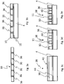
- a workpiece 2 or a substrate is shown, which is arranged in the region of a radiation source 18, in particular a laser, in particular a femtosecond laser (fs laser).
- the workpiece 2 preferably has a first, in particular flat, surface portion 14 and a second, in particular flat, surface portion 16, with the first flat surface portion 14 preferably being aligned essentially or exactly parallel to the second flat surface portion 16.
- the first flat surface portion 14 and the second flat surface portion 16 preferably delimit the workpiece 2 in a Y-direction, which is preferably aligned vertically or plumb.
- the planar surface portions 14 and 16 preferably each extend in an XZ plane, with the XZ plane preferably being oriented horizontally.
- the radiation source 18 emits beams 6 onto the workpiece 2 at the same time or with a time delay.
- the beams 6 penetrate a defined depth into the workpiece 2 and generate local stresses at the respective position or at a predetermined position.
- Fig. 1b a multi-layer arrangement is shown, wherein the workpiece 2 contains the crack-guiding layer 8 and is provided with a holding layer 12 in the area of the first planar surface portion 14, which in turn is preferably overlaid by a further layer 20, with the further layer 20 preferably having a stabilization device, in particular a metal plate.
- a polymer layer 10 is preferably arranged on the second planar surface portion 16 of the workpiece 2 .
- the receiving layer or polymer layer 10 and/or the holding layer 12 preferably consist at least partially and particularly preferably completely of PDMS and particularly preferably has a large number of holes, in particular blind holes and/or through holes.
- In 1c shows a state after crack initiation and subsequent crack development.
- the solid layer 4 adheres to the polymer layer 10 and is or can be spaced apart from the remainder of the workpiece 2 .
- FIG. 2a and 2b are examples of the in Fig. 1a shown production of a crack guide layer 8 by the introduction of local stresses in a workpiece 2, in particular by means of light beams.
- the present invention thus relates to a method for producing solid layers, at least comprising the steps according to claim 1.
- the method according to the invention can additionally include one, several or all of the steps listed below, in particular the provision of a workpiece 2 for separating at least one solid layer 4 , the generation of preferably defined local stresses or local stresses by means of at least one radiation source, in particular an fs laser, in the inner structure of the solid to specify a crack guide layer along which the solid layer is separated from the solid, and the thermal loading of a Polymer layer 10 arranged on the workpiece 2 for, in particular mechanical, generation of detachment stresses in the workpiece 2, with the detachment stresses causing a crack to propagate in the workpiece 2 along the crack-guiding layer 8, which separates the solid-state layer 4 from the W erk Sharing 2 separates include.
- the local tensions preferably cause the crack to propagate in the desired crack guiding layer 8 .
- FIG 2a is thus shown schematically how local stresses 34 can be generated in a workpiece 2, in particular for generating a crack guide layer 8, by means of a radiation source 18, in the case of the present invention by means of at least one femtosecond laser (fs laser), in particular several fs lasers.
- the radiation source 18 emits radiation 6 with a first wavelength 30 and a second wavelength 32.
- the wavelengths 30, 32 are preferably coordinated with one another or the distance between the radiation source 18 and the crack guide layer 8 to be produced is preferably coordinated in such a way that the Waves 30, 32 essentially or exactly meet on the crack guide layer 8 in the workpiece 2, whereby at the point of meeting 34 due to the energies of both waves 30, 32 local stresses or defects are generated.
- the local stresses can be generated by different or combined mechanisms, such as sublimation, melting and/or chemical reaction.
- a focused light beam 6 is shown, the focus of which is preferably in the crack guide layer 8 . It is conceivable here that the light beam 6 is focused by one or more focusing bodies, in particular lens(es) (not shown).
- the workpiece 2 has a multilayer design and preferably has a partially transparent or transparent substrate layer 3 or material layer, which preferably consists of sapphire or has sapphire.
- the light beams 6 pass through the substrate layer 3 onto the crack guide layer 8, which is preferably formed by a sacrificial layer 5, the sacrificial layer 5 being exposed to the radiation in such a way that the generation of local stresses in the sacrificial layer 5 at the focal point or in the Area of focus is effected.
- the local stresses for producing the crack guide layer 8 are produced in the area or precisely on an interface between two layers 3, 4. It is thus also conceivable that the solid layer 4 is produced on a carrier layer, in particular a substrate layer 3, and by means of one or more sacrificial layers 5 and/or by means of the generation of local stresses in an interface, in particular between the solid layer 4 and the carrier layer. a crack guiding layer 8 for detaching or separating the solid layer 4 can be produced.
- Figure 3a shows a recording layer 10 or film according to the invention for generating stress in a solid.
- the film has at least one polymer material, in particular PDMS, with the polymer material having a lower glass transition at a temperature than 0°C, especially at a temperature below -50°C.
- the foil has a plurality of holes 36 for directing a liquid through the foil, the holes 36 each having a diameter of less than 0.1 mm.
- Figure 3b shows a solid 2 and a solid layer 4 separated from it.
- a receiving layer 10 or a film 10 is also arranged on the solid layer 4, by means of which the stresses required to produce a crack for separating the solid layer 4 from the solid 2 were generated.
- the absorption layer 10 has a multiplicity of holes for guiding a liquid, the absorption layer 10 being fixed to the solid layer 4 by means of a bonding layer 11 .
- 3c 1 shows, as an example for illustration, a receiving layer 10 or foil, which can be arranged or is arranged on the solid body 4, preferably likewise by means of a connecting layer 11.
- the receiving layer 10 preferably has a first material portion 39, in particular a polymer portion, and a second material portion 40, in particular a metal portion.
- the second material portion 40 preferably represents a coating of the first material portion 39 and is particularly preferably used for accelerated cooling of the first material portion 39.
- the recording layer 10 is preferably exposed to cold, in particular liquid nitrogen, from direction 38, whereby the second material portion 40 quickly cools down and, in particular, due to the direct contact with the first material portion 39, it is also cooled very quickly.
- 3d 1 shows, as a further illustrative example, an absorption layer 10 or film, which in turn is formed by the first material portion 39 and the second material portion 40.
- the first portion of material 39 has holes 36 which are filled by the second portion of material 40 .
- the second material portion 40 preferably also coats the first material portion 39 on the top side, i.e. parallel to the connecting layer 11.
- Figure 3e shows a further variant of the receiving layer 10 or film according to the invention, which in turn is formed by the first material portion 39 and the second material portion 40 .
- the first portion of material 39 has holes 36 which are lined by the second portion of material 40, ie the wall delimiting the respective hole 36 is coated with the second portion of material.
- the second material portion 40 preferably also coats the first material portion 39 on the top side, i.e. parallel to the connecting layer 11.
- the method for producing of solid layers comprises: providing a solid 2 for separating at least one solid layer 4, arranging an acquisition layer 10 for holding the solid layer 4 on the solid 2, the acquisition layer consisting of at least one polymer and another material, the acquisition layer preferably being the majority in terms of volume and/or mass consists of the polymer, with the other material having a higher conductivity than the polymer, thermal loading of the receiving layer 10 to generate, in particular mechanical, stresses in the solid body 2, the stresses causing a crack in the solid body 2 along a detachment plane 8 spreads, the solid layer 4 being separated from the solid 2 by the crack.
- the film according to the invention for generating stress in a solid has at least one polymer material, in particular PDMS, and a further material, with the film largely consisting of the polymer material in terms of volume, with the further material having a greater thermal conductivity than the polymer material, with the polymer material having a glass transition at a temperature of less than 0°C, in particular at a temperature of less than -50°C, the film having a large number of holes for conducting a liquid through the film, the holes each having a diameter of less than 0, have 1 mm.
Landscapes
- Engineering & Computer Science (AREA)
- Mechanical Engineering (AREA)
- Dicing (AREA)
- Manufacturing & Machinery (AREA)
- Laser Beam Processing (AREA)
- Processing Of Stones Or Stones Resemblance Materials (AREA)
Claims (13)
- Procédé de fabrication de couches de corps solide, comprenant au moins les stades :on se procure un corps (2) solide pour la séparation d'au moins une couche (4) de corps solide ;on fixe une couche (10) de réception pour le maintien de la couche (4) de corps solide sur le corps (2) solide, dans lequel on fixe la couche (10) de réception sur le corps (2) solide au moyen d'une couche (11) de liaison, dans lequel la couche (10) de réception a au moins un matériau polymère, le matériau polymère subissant une transition à l'état vitreux à une température plus basse que 0°C et la couche (10) de réception ayant une pluralité de trous (36) d'un diamètre de moins de 0,1 mm pour envoyer un fluide à la couche (11) de liaison à travers la couche (10) de réception ;on produit des défauts dans la structure intérieure du corps (2) solide pour la prescription d'un plan (8) de détachement au moyen d'au moins un laser (18) à femtoseconde avant ou après la fixation de la couche (10) de réception au corps (2) solide ;et on sollicite thermiquement la couche (10) de réception pour la production de tensions dans le corps (2) solide, dans lequel par les tensions une fissure dans le corps (2) solide se propage le long du plan (8) de détachement, dans lequel par la fissure on sépare la couche (4) de corps solide du corps (2) solide.
- Procédé suivant la revendication 1,
dans lequel
la couche de réception a plus de 10 trous (36), de préférence plus de 100 trous (36) et, d'une manière particulièrement préférée, plus de 1000 trous (36). - Procédé suivant l'une des revendications précédentes,
dans lequel
au moins un autre trou est constitué autour du centre d'un trou dans un rayon de moins de 50 mm, de préférence de moins de 25 mm et, d'une manière particulièrement préférée, de moins de 5 mm. - Procédé suivant l'une des revendications précédentes,
dans lequel
pour détacher la couche (10) de réception du corps (4) solide on envoie un fluide, notamment un liquide dans les trous de la couche (11) de liaison, dans lequel le fluide fait que la fixation de la couche (10) de réception à la couche (4) de corps solide est affaiblie ou supprimée. - Procédé suivant la revendication 4,
dans lequel
on règle le laser (18) à femtoseconde de manière à ce que le rayonnement (6) qu'il émet pour la production du plan (8) de détachement pénètre à une profondeur définie de moins de 200 µm, de préférence de moins de 100 µm et, d'une manière particulièrement préférée, de moins de 50 µm et, d'une manière encore plus particulièrement préférée, de moins de 20 µm, dans le corps (2) solide. - Procédé suivant la revendication 4,
dans lequel
on règle le laser (18) à femtoseconde de manière à ce que le rayonnement (6) qu'il émet pour produire le plan (8) de détachement pénètre dans le corps (2) solide à une profondeur définie de plus de 100 µm, de préférence de plus de 200 µm et, d'une manière encore plus préférée, de plus de 400 µm et, d'une manière particulièrement préférée, de plus de 700 µm. - Procédé suivant l'une des revendications 4 à 6,
dans lequel
le laser (18) à femtoseconde a une durée de pulsation de moins de 500 fs. - Procédé suivant l'une des revendications précédentes 4 à 7,
dans lequel
on choisit l'énergie du faisceau laser à femtoseconde de manière à ce que la propagation d'un dommage dans le corps (2) solide soit plus petite que trois fois la longueur de Rayleigh, de préférence plus petite que la longueur de Rayleigh et, d'une manière particulièrement préférée, plus petite qu'un tiers de la longueur de Rayleigh. - Procédé suivant l'une des revendications 4 à 8 précédentes,
dans lequel
on choisit la longueur d'onde du faisceau du laser à femtoseconde de manière à ce que l'absorption du corps (2) solide soit plus petite que 10cm-1 et, d'une manière préférée, plus petite que 1cm-1 et, d'une manière particulièrement préférée, plus petite que 0,1cm-1. - Procédé suivant l'une des revendications 4 à 9 précédentes,
dans lequel
les divers défauts se produisent respectivement à la suite d'une excitation multiphotonique provoquée par le laser à femtoseconde. - Montage ayant une couche (10) de réception, comportant :un corps (2) solide ayant un plan (8) de détachement prescrit par des défauts dans la structure intérieure du corps (2) solide, dans lequel les défauts ont été produits au moyen d'au moins un laser (18) à femtoseconde avant ou après la fixation de la couche (10) de réception sur le corps (2) solide ;une couche (11) de liaison sur une surface du corps (2) solide, la couche (10) de réception sur la couche (11) de liaison étant fixée au corps (2) solide par la couche (11) de liaison, la couche (10) de réception ayant au moins un matériau polymère, le matériau polymère subissant une transition d'état vitreux à une température plus basse que 0°C, une sollicitation thermique de la couche (10) de réception conduisant à la production de tensions dans le corps (2) solide, dans lequel par les tensions une fissure se propage dans le corps (2) solide le long du plan (8) de détachement, dans lequel par la fissure la couche (4) de corps solide est séparée du corps (2) solide et dans lequel la couche (10) de réception a une pluralité de trous (36) d'un diamètre de moins de 0,1 mm pour envoyer un fluide à la couche (11) de liaison.
- Feuille réutilisable de production de tensions dans un corps solide,dans laquelle la feuille a au moins un matériau polymère, notamment du PDMS, le matériau polymère subissant une transition à l'état vitreux à une température plus basse que 0°C, notamment à une température plus basse que - 50°C,caractérisée en ce quela feuille a une pluralité de trous pour le passage d'un liquide à travers la feuille, les trous ayant chacun un diamètre de moins de 0,1 mm.
- Utilisation d'une feuille suivant la revendication 12 comme couche de réception dans un procédé suivant la revendication 1.
Applications Claiming Priority (2)
| Application Number | Priority Date | Filing Date | Title |
|---|---|---|---|
| DE102014014422.4A DE102014014422A1 (de) | 2014-09-29 | 2014-09-29 | Kombiniertes Waferherstellungsverfahren mit einer Löcher aufweisenden Aufnahmeschicht |
| PCT/EP2015/071948 WO2016050596A1 (fr) | 2014-09-29 | 2015-09-24 | Procédé combiné de fabrication de tranches au moyen d'une couche réceptrice pourvue de trous |
Publications (2)
| Publication Number | Publication Date |
|---|---|
| EP3201941A1 EP3201941A1 (fr) | 2017-08-09 |
| EP3201941B1 true EP3201941B1 (fr) | 2022-12-21 |
Family
ID=54151291
Family Applications (1)
| Application Number | Title | Priority Date | Filing Date |
|---|---|---|---|
| EP15767167.8A Active EP3201941B1 (fr) | 2014-09-29 | 2015-09-24 | Procédé combiné de fabrication de tranches au moyen d'une couche réceptrice pourvue de trous |
Country Status (4)
| Country | Link |
|---|---|
| US (1) | US10960574B2 (fr) |
| EP (1) | EP3201941B1 (fr) |
| DE (1) | DE102014014422A1 (fr) |
| WO (1) | WO2016050596A1 (fr) |
Families Citing this family (2)
| Publication number | Priority date | Publication date | Assignee | Title |
|---|---|---|---|---|
| DE102015008034A1 (de) * | 2015-06-23 | 2016-12-29 | Siltectra Gmbh | Verfahren zum Führen eines Risses im Randbereich eines Spendersubstrats |
| DE102023200449A1 (de) | 2023-01-20 | 2024-07-25 | Infineon Technologies Ag | Vorrichtung und verfahren zum spalten eines halbleiterwafers |
Citations (2)
| Publication number | Priority date | Publication date | Assignee | Title |
|---|---|---|---|---|
| US20110259936A1 (en) * | 2008-12-23 | 2011-10-27 | Siltectra Gmbh | Method for producing thin, free-standing layers of solid state materials with structured surfaces |
| DE102012001620A1 (de) * | 2012-01-30 | 2013-08-01 | Siltectra Gmbh | Verfahren zur Herstellung von dünnen Platten aus Werkstoffen geringer Duktilität mittels temperaturinduzierter mechanischer Spannung unter Verwendung von vorgefertigten Polymer-Folien |
Family Cites Families (8)
| Publication number | Priority date | Publication date | Assignee | Title |
|---|---|---|---|---|
| US6214733B1 (en) | 1999-11-17 | 2001-04-10 | Elo Technologies, Inc. | Process for lift off and handling of thin film materials |
| FR2837620B1 (fr) | 2002-03-25 | 2005-04-29 | Commissariat Energie Atomique | Procede de transfert d'elements de substrat a substrat |
| FR2877142B1 (fr) * | 2004-10-21 | 2007-05-11 | Commissariat Energie Atomique | Procede de transfert d'au moins un objet de taille micrometrique ou millimetrique au moyen d'une poignee en polymere. |
| JP5117692B2 (ja) | 2006-07-14 | 2013-01-16 | ルネサスエレクトロニクス株式会社 | 半導体装置の製造方法 |
| JP5460984B2 (ja) * | 2007-08-17 | 2014-04-02 | 株式会社半導体エネルギー研究所 | 半導体装置の作製方法 |
| JP5590837B2 (ja) | 2009-09-15 | 2014-09-17 | キヤノン株式会社 | 機能性領域の移設方法 |
| DE102010030358B4 (de) * | 2010-06-22 | 2014-05-22 | Osram Opto Semiconductors Gmbh | Verfahren zum Abtrennen einer Substratscheibe |
| DE102014013107A1 (de) | 2013-10-08 | 2015-04-09 | Siltectra Gmbh | Neuartiges Waferherstellungsverfahren |
-
2014
- 2014-09-29 DE DE102014014422.4A patent/DE102014014422A1/de not_active Withdrawn
-
2015
- 2015-09-24 EP EP15767167.8A patent/EP3201941B1/fr active Active
- 2015-09-24 US US15/515,520 patent/US10960574B2/en active Active
- 2015-09-24 WO PCT/EP2015/071948 patent/WO2016050596A1/fr not_active Ceased
Patent Citations (2)
| Publication number | Priority date | Publication date | Assignee | Title |
|---|---|---|---|---|
| US20110259936A1 (en) * | 2008-12-23 | 2011-10-27 | Siltectra Gmbh | Method for producing thin, free-standing layers of solid state materials with structured surfaces |
| DE102012001620A1 (de) * | 2012-01-30 | 2013-08-01 | Siltectra Gmbh | Verfahren zur Herstellung von dünnen Platten aus Werkstoffen geringer Duktilität mittels temperaturinduzierter mechanischer Spannung unter Verwendung von vorgefertigten Polymer-Folien |
Also Published As
| Publication number | Publication date |
|---|---|
| EP3201941A1 (fr) | 2017-08-09 |
| US10960574B2 (en) | 2021-03-30 |
| US20170217048A1 (en) | 2017-08-03 |
| DE102014014422A1 (de) | 2016-03-31 |
| WO2016050596A1 (fr) | 2016-04-07 |
Similar Documents
| Publication | Publication Date | Title |
|---|---|---|
| EP3280577B1 (fr) | Procédé de fabrication de tranches avec economie de materiaux | |
| EP3055098B1 (fr) | Procédé de fabrication de tranches de silicium | |
| EP3055447B1 (fr) | Création d'un point de départ de fissure ou d'un guide de fissuration afin de permettre un meilleur détachement d'une couche de solide à partir d'un solide | |
| EP3055448B1 (fr) | Procédé de production combiné permettant de séparer plusieurs couches de solide minces à partir d'un solide épais | |
| EP3223993A2 (fr) | Séparation de corps solide au moyen de la transformation de matière | |
| EP3245665B1 (fr) | Procédé pour fabriquer une tranche irrégulière | |
| DE102014002600A1 (de) | Kombiniertes Waferherstellungsverfahren mit Laserbehandlung und temperaturinduzierten Spannungen | |
| DE102015004603A1 (de) | Kombiniertes Waferherstellungsverfahren mit Laserbehandlung und temperaturinduzierten Spannungen | |
| EP3147068B1 (fr) | Nouveau procédé de fabrication de tranches | |
| EP3137657B1 (fr) | Procédé combiné de fabrication de corps solides par traitement au laser et tensions thermo-induites pour la production de corps solides tridimensionnels | |
| EP3433876B1 (fr) | Un procédé de division | |
| EP3201941B1 (fr) | Procédé combiné de fabrication de tranches au moyen d'une couche réceptrice pourvue de trous | |
| EP3186824B1 (fr) | Procédé de division et utilisation d'un matériau dans un procédé de division | |
| EP3201944B1 (fr) | Procédé combiné de fabrication de tranches au moyen d'une couche réceptrice à plusieurs constituants | |
| EP3608048B1 (fr) | Procédé de fabrication d'éléments de corps solide au moyen du traitement laser et de contraintes induites par la température | |
| DE102013014623A1 (de) | Vorrichtung und Verfahren zur Herstellung eines Wafers mit einer selektiven Positionierung im Trägersystem | |
| DE102016105616A1 (de) | Polymer-Hybrid-Material, dessen Verwendung in einem Splitting-Verfahren und Verfahren zur Herstellung des Polymer-Hybrid-Materials |
Legal Events
| Date | Code | Title | Description |
|---|---|---|---|
| STAA | Information on the status of an ep patent application or granted ep patent |
Free format text: STATUS: THE INTERNATIONAL PUBLICATION HAS BEEN MADE |
|
| PUAI | Public reference made under article 153(3) epc to a published international application that has entered the european phase |
Free format text: ORIGINAL CODE: 0009012 |
|
| STAA | Information on the status of an ep patent application or granted ep patent |
Free format text: STATUS: REQUEST FOR EXAMINATION WAS MADE |
|
| 17P | Request for examination filed |
Effective date: 20170502 |
|
| AK | Designated contracting states |
Kind code of ref document: A1 Designated state(s): AL AT BE BG CH CY CZ DE DK EE ES FI FR GB GR HR HU IE IS IT LI LT LU LV MC MK MT NL NO PL PT RO RS SE SI SK SM TR |
|
| AX | Request for extension of the european patent |
Extension state: BA ME |
|
| DAV | Request for validation of the european patent (deleted) | ||
| DAX | Request for extension of the european patent (deleted) | ||
| RAP1 | Party data changed (applicant data changed or rights of an application transferred) |
Owner name: SILTECTRA GMBH |
|
| RIN1 | Information on inventor provided before grant (corrected) |
Inventor name: AJAJ, ANAS Inventor name: RICHTER, JAN Inventor name: BEYER, CHRISTIAN |
|
| RAP1 | Party data changed (applicant data changed or rights of an application transferred) |
Owner name: SILTECTRA GMBH |
|
| RAP1 | Party data changed (applicant data changed or rights of an application transferred) |
Owner name: SILTECTRA GMBH |
|
| STAA | Information on the status of an ep patent application or granted ep patent |
Free format text: STATUS: EXAMINATION IS IN PROGRESS |
|
| 17Q | First examination report despatched |
Effective date: 20210316 |
|
| REG | Reference to a national code |
Ref country code: DE Ref legal event code: R079 Ref document number: 502015016210 Country of ref document: DE Free format text: PREVIOUS MAIN CLASS: H01L0021200000 Ipc: H01L0021020000 |
|
| RIC1 | Information provided on ipc code assigned before grant |
Ipc: H01L 21/304 20060101ALI20220714BHEP Ipc: H01L 21/02 20060101AFI20220714BHEP |
|
| GRAP | Despatch of communication of intention to grant a patent |
Free format text: ORIGINAL CODE: EPIDOSNIGR1 |
|
| STAA | Information on the status of an ep patent application or granted ep patent |
Free format text: STATUS: GRANT OF PATENT IS INTENDED |
|
| INTG | Intention to grant announced |
Effective date: 20220908 |
|
| GRAS | Grant fee paid |
Free format text: ORIGINAL CODE: EPIDOSNIGR3 |
|
| GRAA | (expected) grant |
Free format text: ORIGINAL CODE: 0009210 |
|
| STAA | Information on the status of an ep patent application or granted ep patent |
Free format text: STATUS: THE PATENT HAS BEEN GRANTED |
|
| AK | Designated contracting states |
Kind code of ref document: B1 Designated state(s): AL AT BE BG CH CY CZ DE DK EE ES FI FR GB GR HR HU IE IS IT LI LT LU LV MC MK MT NL NO PL PT RO RS SE SI SK SM TR |
|
| REG | Reference to a national code |
Ref country code: GB Ref legal event code: FG4D Free format text: NOT ENGLISH |
|
| REG | Reference to a national code |
Ref country code: DE Ref legal event code: R096 Ref document number: 502015016210 Country of ref document: DE |
|
| REG | Reference to a national code |
Ref country code: CH Ref legal event code: EP |
|
| REG | Reference to a national code |
Ref country code: AT Ref legal event code: REF Ref document number: 1539558 Country of ref document: AT Kind code of ref document: T Effective date: 20230115 |
|
| REG | Reference to a national code |
Ref country code: IE Ref legal event code: FG4D Free format text: LANGUAGE OF EP DOCUMENT: GERMAN |
|
| REG | Reference to a national code |
Ref country code: LT Ref legal event code: MG9D |
|
| REG | Reference to a national code |
Ref country code: NL Ref legal event code: MP Effective date: 20221221 |
|
| PG25 | Lapsed in a contracting state [announced via postgrant information from national office to epo] |
Ref country code: SE Free format text: LAPSE BECAUSE OF FAILURE TO SUBMIT A TRANSLATION OF THE DESCRIPTION OR TO PAY THE FEE WITHIN THE PRESCRIBED TIME-LIMIT Effective date: 20221221 Ref country code: NO Free format text: LAPSE BECAUSE OF FAILURE TO SUBMIT A TRANSLATION OF THE DESCRIPTION OR TO PAY THE FEE WITHIN THE PRESCRIBED TIME-LIMIT Effective date: 20230321 Ref country code: LT Free format text: LAPSE BECAUSE OF FAILURE TO SUBMIT A TRANSLATION OF THE DESCRIPTION OR TO PAY THE FEE WITHIN THE PRESCRIBED TIME-LIMIT Effective date: 20221221 Ref country code: FI Free format text: LAPSE BECAUSE OF FAILURE TO SUBMIT A TRANSLATION OF THE DESCRIPTION OR TO PAY THE FEE WITHIN THE PRESCRIBED TIME-LIMIT Effective date: 20221221 |
|
| PG25 | Lapsed in a contracting state [announced via postgrant information from national office to epo] |
Ref country code: RS Free format text: LAPSE BECAUSE OF FAILURE TO SUBMIT A TRANSLATION OF THE DESCRIPTION OR TO PAY THE FEE WITHIN THE PRESCRIBED TIME-LIMIT Effective date: 20221221 Ref country code: LV Free format text: LAPSE BECAUSE OF FAILURE TO SUBMIT A TRANSLATION OF THE DESCRIPTION OR TO PAY THE FEE WITHIN THE PRESCRIBED TIME-LIMIT Effective date: 20221221 Ref country code: HR Free format text: LAPSE BECAUSE OF FAILURE TO SUBMIT A TRANSLATION OF THE DESCRIPTION OR TO PAY THE FEE WITHIN THE PRESCRIBED TIME-LIMIT Effective date: 20221221 Ref country code: GR Free format text: LAPSE BECAUSE OF FAILURE TO SUBMIT A TRANSLATION OF THE DESCRIPTION OR TO PAY THE FEE WITHIN THE PRESCRIBED TIME-LIMIT Effective date: 20230322 |
|
| PG25 | Lapsed in a contracting state [announced via postgrant information from national office to epo] |
Ref country code: NL Free format text: LAPSE BECAUSE OF FAILURE TO SUBMIT A TRANSLATION OF THE DESCRIPTION OR TO PAY THE FEE WITHIN THE PRESCRIBED TIME-LIMIT Effective date: 20221221 |
|
| P01 | Opt-out of the competence of the unified patent court (upc) registered |
Effective date: 20230528 |
|
| PG25 | Lapsed in a contracting state [announced via postgrant information from national office to epo] |
Ref country code: SM Free format text: LAPSE BECAUSE OF FAILURE TO SUBMIT A TRANSLATION OF THE DESCRIPTION OR TO PAY THE FEE WITHIN THE PRESCRIBED TIME-LIMIT Effective date: 20221221 Ref country code: RO Free format text: LAPSE BECAUSE OF FAILURE TO SUBMIT A TRANSLATION OF THE DESCRIPTION OR TO PAY THE FEE WITHIN THE PRESCRIBED TIME-LIMIT Effective date: 20221221 Ref country code: PT Free format text: LAPSE BECAUSE OF FAILURE TO SUBMIT A TRANSLATION OF THE DESCRIPTION OR TO PAY THE FEE WITHIN THE PRESCRIBED TIME-LIMIT Effective date: 20230421 Ref country code: ES Free format text: LAPSE BECAUSE OF FAILURE TO SUBMIT A TRANSLATION OF THE DESCRIPTION OR TO PAY THE FEE WITHIN THE PRESCRIBED TIME-LIMIT Effective date: 20221221 Ref country code: EE Free format text: LAPSE BECAUSE OF FAILURE TO SUBMIT A TRANSLATION OF THE DESCRIPTION OR TO PAY THE FEE WITHIN THE PRESCRIBED TIME-LIMIT Effective date: 20221221 Ref country code: CZ Free format text: LAPSE BECAUSE OF FAILURE TO SUBMIT A TRANSLATION OF THE DESCRIPTION OR TO PAY THE FEE WITHIN THE PRESCRIBED TIME-LIMIT Effective date: 20221221 |
|
| PG25 | Lapsed in a contracting state [announced via postgrant information from national office to epo] |
Ref country code: SK Free format text: LAPSE BECAUSE OF FAILURE TO SUBMIT A TRANSLATION OF THE DESCRIPTION OR TO PAY THE FEE WITHIN THE PRESCRIBED TIME-LIMIT Effective date: 20221221 Ref country code: PL Free format text: LAPSE BECAUSE OF FAILURE TO SUBMIT A TRANSLATION OF THE DESCRIPTION OR TO PAY THE FEE WITHIN THE PRESCRIBED TIME-LIMIT Effective date: 20221221 Ref country code: IS Free format text: LAPSE BECAUSE OF FAILURE TO SUBMIT A TRANSLATION OF THE DESCRIPTION OR TO PAY THE FEE WITHIN THE PRESCRIBED TIME-LIMIT Effective date: 20230421 Ref country code: AL Free format text: LAPSE BECAUSE OF FAILURE TO SUBMIT A TRANSLATION OF THE DESCRIPTION OR TO PAY THE FEE WITHIN THE PRESCRIBED TIME-LIMIT Effective date: 20221221 |
|
| REG | Reference to a national code |
Ref country code: DE Ref legal event code: R097 Ref document number: 502015016210 Country of ref document: DE |
|
| PLBE | No opposition filed within time limit |
Free format text: ORIGINAL CODE: 0009261 |
|
| STAA | Information on the status of an ep patent application or granted ep patent |
Free format text: STATUS: NO OPPOSITION FILED WITHIN TIME LIMIT |
|
| PG25 | Lapsed in a contracting state [announced via postgrant information from national office to epo] |
Ref country code: DK Free format text: LAPSE BECAUSE OF FAILURE TO SUBMIT A TRANSLATION OF THE DESCRIPTION OR TO PAY THE FEE WITHIN THE PRESCRIBED TIME-LIMIT Effective date: 20221221 |
|
| 26N | No opposition filed |
Effective date: 20230922 |
|
| PG25 | Lapsed in a contracting state [announced via postgrant information from national office to epo] |
Ref country code: SI Free format text: LAPSE BECAUSE OF FAILURE TO SUBMIT A TRANSLATION OF THE DESCRIPTION OR TO PAY THE FEE WITHIN THE PRESCRIBED TIME-LIMIT Effective date: 20221221 |
|
| REG | Reference to a national code |
Ref country code: CH Ref legal event code: PL |
|
| PG25 | Lapsed in a contracting state [announced via postgrant information from national office to epo] |
Ref country code: LU Free format text: LAPSE BECAUSE OF NON-PAYMENT OF DUE FEES Effective date: 20230924 |
|
| REG | Reference to a national code |
Ref country code: BE Ref legal event code: MM Effective date: 20230930 |
|
| GBPC | Gb: european patent ceased through non-payment of renewal fee |
Effective date: 20230924 |
|
| PG25 | Lapsed in a contracting state [announced via postgrant information from national office to epo] |
Ref country code: LU Free format text: LAPSE BECAUSE OF NON-PAYMENT OF DUE FEES Effective date: 20230924 Ref country code: IT Free format text: LAPSE BECAUSE OF FAILURE TO SUBMIT A TRANSLATION OF THE DESCRIPTION OR TO PAY THE FEE WITHIN THE PRESCRIBED TIME-LIMIT Effective date: 20221221 Ref country code: MC Free format text: LAPSE BECAUSE OF FAILURE TO SUBMIT A TRANSLATION OF THE DESCRIPTION OR TO PAY THE FEE WITHIN THE PRESCRIBED TIME-LIMIT Effective date: 20221221 |
|
| REG | Reference to a national code |
Ref country code: IE Ref legal event code: MM4A |
|
| PG25 | Lapsed in a contracting state [announced via postgrant information from national office to epo] |
Ref country code: IE Free format text: LAPSE BECAUSE OF NON-PAYMENT OF DUE FEES Effective date: 20230924 |
|
| PG25 | Lapsed in a contracting state [announced via postgrant information from national office to epo] |
Ref country code: GB Free format text: LAPSE BECAUSE OF NON-PAYMENT OF DUE FEES Effective date: 20230924 |
|
| PG25 | Lapsed in a contracting state [announced via postgrant information from national office to epo] |
Ref country code: CH Free format text: LAPSE BECAUSE OF NON-PAYMENT OF DUE FEES Effective date: 20230930 |
|
| PG25 | Lapsed in a contracting state [announced via postgrant information from national office to epo] |
Ref country code: IE Free format text: LAPSE BECAUSE OF NON-PAYMENT OF DUE FEES Effective date: 20230924 Ref country code: GB Free format text: LAPSE BECAUSE OF NON-PAYMENT OF DUE FEES Effective date: 20230924 Ref country code: FR Free format text: LAPSE BECAUSE OF NON-PAYMENT OF DUE FEES Effective date: 20230930 Ref country code: CH Free format text: LAPSE BECAUSE OF NON-PAYMENT OF DUE FEES Effective date: 20230930 |
|
| PG25 | Lapsed in a contracting state [announced via postgrant information from national office to epo] |
Ref country code: BE Free format text: LAPSE BECAUSE OF NON-PAYMENT OF DUE FEES Effective date: 20230930 |
|
| PG25 | Lapsed in a contracting state [announced via postgrant information from national office to epo] |
Ref country code: BG Free format text: LAPSE BECAUSE OF FAILURE TO SUBMIT A TRANSLATION OF THE DESCRIPTION OR TO PAY THE FEE WITHIN THE PRESCRIBED TIME-LIMIT Effective date: 20221221 |
|
| REG | Reference to a national code |
Ref country code: AT Ref legal event code: MM01 Ref document number: 1539558 Country of ref document: AT Kind code of ref document: T Effective date: 20230924 |
|
| PG25 | Lapsed in a contracting state [announced via postgrant information from national office to epo] |
Ref country code: BG Free format text: LAPSE BECAUSE OF FAILURE TO SUBMIT A TRANSLATION OF THE DESCRIPTION OR TO PAY THE FEE WITHIN THE PRESCRIBED TIME-LIMIT Effective date: 20221221 |
|
| PG25 | Lapsed in a contracting state [announced via postgrant information from national office to epo] |
Ref country code: AT Free format text: LAPSE BECAUSE OF NON-PAYMENT OF DUE FEES Effective date: 20230924 |
|
| PG25 | Lapsed in a contracting state [announced via postgrant information from national office to epo] |
Ref country code: AT Free format text: LAPSE BECAUSE OF NON-PAYMENT OF DUE FEES Effective date: 20230924 |
|
| PG25 | Lapsed in a contracting state [announced via postgrant information from national office to epo] |
Ref country code: CY Free format text: LAPSE BECAUSE OF FAILURE TO SUBMIT A TRANSLATION OF THE DESCRIPTION OR TO PAY THE FEE WITHIN THE PRESCRIBED TIME-LIMIT; INVALID AB INITIO Effective date: 20150924 |
|
| PG25 | Lapsed in a contracting state [announced via postgrant information from national office to epo] |
Ref country code: HU Free format text: LAPSE BECAUSE OF FAILURE TO SUBMIT A TRANSLATION OF THE DESCRIPTION OR TO PAY THE FEE WITHIN THE PRESCRIBED TIME-LIMIT; INVALID AB INITIO Effective date: 20150924 |
|
| REG | Reference to a national code |
Ref country code: DE Ref legal event code: R079 Ref document number: 502015016210 Country of ref document: DE Free format text: PREVIOUS MAIN CLASS: H01L0021020000 Ipc: H10P0095000000 |
|
| PG25 | Lapsed in a contracting state [announced via postgrant information from national office to epo] |
Ref country code: TR Free format text: LAPSE BECAUSE OF FAILURE TO SUBMIT A TRANSLATION OF THE DESCRIPTION OR TO PAY THE FEE WITHIN THE PRESCRIBED TIME-LIMIT Effective date: 20221221 |
|
| PGFP | Annual fee paid to national office [announced via postgrant information from national office to epo] |
Ref country code: DE Payment date: 20251121 Year of fee payment: 11 |