EP3201989B1 - Draht und verfahren zur herstellung eines drahtes zur aufnahme eines kontaktelements - Google Patents
Draht und verfahren zur herstellung eines drahtes zur aufnahme eines kontaktelements Download PDFInfo
- Publication number
- EP3201989B1 EP3201989B1 EP15847577.2A EP15847577A EP3201989B1 EP 3201989 B1 EP3201989 B1 EP 3201989B1 EP 15847577 A EP15847577 A EP 15847577A EP 3201989 B1 EP3201989 B1 EP 3201989B1
- Authority
- EP
- European Patent Office
- Prior art keywords
- conductor
- foil layer
- conductive foil
- exposed portion
- wire
- Prior art date
- Legal status (The legal status is an assumption and is not a legal conclusion. Google has not performed a legal analysis and makes no representation as to the accuracy of the status listed.)
- Active
Links
Images


Classifications
-
- H—ELECTRICITY
- H01—ELECTRIC ELEMENTS
- H01R—ELECTRICALLY-CONDUCTIVE CONNECTIONS; STRUCTURAL ASSOCIATIONS OF A PLURALITY OF MUTUALLY-INSULATED ELECTRICAL CONNECTING ELEMENTS; COUPLING DEVICES; CURRENT COLLECTORS
- H01R4/00—Electrically-conductive connections between two or more conductive members in direct contact, i.e. touching one another; Means for effecting or maintaining such contact; Electrically-conductive connections having two or more spaced connecting locations for conductors and using contact members penetrating insulation
- H01R4/10—Electrically-conductive connections between two or more conductive members in direct contact, i.e. touching one another; Means for effecting or maintaining such contact; Electrically-conductive connections having two or more spaced connecting locations for conductors and using contact members penetrating insulation effected solely by twisting, wrapping, bending, crimping, or other permanent deformation
- H01R4/18—Electrically-conductive connections between two or more conductive members in direct contact, i.e. touching one another; Means for effecting or maintaining such contact; Electrically-conductive connections having two or more spaced connecting locations for conductors and using contact members penetrating insulation effected solely by twisting, wrapping, bending, crimping, or other permanent deformation by crimping
- H01R4/183—Electrically-conductive connections between two or more conductive members in direct contact, i.e. touching one another; Means for effecting or maintaining such contact; Electrically-conductive connections having two or more spaced connecting locations for conductors and using contact members penetrating insulation effected solely by twisting, wrapping, bending, crimping, or other permanent deformation by crimping for cylindrical elongated bodies, e.g. cables having circular cross-section
- H01R4/184—Electrically-conductive connections between two or more conductive members in direct contact, i.e. touching one another; Means for effecting or maintaining such contact; Electrically-conductive connections having two or more spaced connecting locations for conductors and using contact members penetrating insulation effected solely by twisting, wrapping, bending, crimping, or other permanent deformation by crimping for cylindrical elongated bodies, e.g. cables having circular cross-section comprising a U-shaped wire-receiving portion
-
- H—ELECTRICITY
- H01—ELECTRIC ELEMENTS
- H01B—CABLES; CONDUCTORS; INSULATORS; SELECTION OF MATERIALS FOR THEIR CONDUCTIVE, INSULATING OR DIELECTRIC PROPERTIES
- H01B1/00—Conductors or conductive bodies characterised by the conductive materials; Selection of materials as conductors
- H01B1/02—Conductors or conductive bodies characterised by the conductive materials; Selection of materials as conductors mainly consisting of metals or alloys
- H01B1/023—Alloys based on aluminium
-
- H—ELECTRICITY
- H01—ELECTRIC ELEMENTS
- H01B—CABLES; CONDUCTORS; INSULATORS; SELECTION OF MATERIALS FOR THEIR CONDUCTIVE, INSULATING OR DIELECTRIC PROPERTIES
- H01B1/00—Conductors or conductive bodies characterised by the conductive materials; Selection of materials as conductors
- H01B1/02—Conductors or conductive bodies characterised by the conductive materials; Selection of materials as conductors mainly consisting of metals or alloys
- H01B1/026—Alloys based on copper
-
- H—ELECTRICITY
- H01—ELECTRIC ELEMENTS
- H01B—CABLES; CONDUCTORS; INSULATORS; SELECTION OF MATERIALS FOR THEIR CONDUCTIVE, INSULATING OR DIELECTRIC PROPERTIES
- H01B7/00—Insulated conductors or cables characterised by their form
- H01B7/17—Protection against damage caused by external factors, e.g. sheaths or armouring
- H01B7/28—Protection against damage caused by moisture, corrosion, chemical attack or weather
- H01B7/2806—Protection against damage caused by corrosion
-
- H—ELECTRICITY
- H01—ELECTRIC ELEMENTS
- H01R—ELECTRICALLY-CONDUCTIVE CONNECTIONS; STRUCTURAL ASSOCIATIONS OF A PLURALITY OF MUTUALLY-INSULATED ELECTRICAL CONNECTING ELEMENTS; COUPLING DEVICES; CURRENT COLLECTORS
- H01R4/00—Electrically-conductive connections between two or more conductive members in direct contact, i.e. touching one another; Means for effecting or maintaining such contact; Electrically-conductive connections having two or more spaced connecting locations for conductors and using contact members penetrating insulation
- H01R4/10—Electrically-conductive connections between two or more conductive members in direct contact, i.e. touching one another; Means for effecting or maintaining such contact; Electrically-conductive connections having two or more spaced connecting locations for conductors and using contact members penetrating insulation effected solely by twisting, wrapping, bending, crimping, or other permanent deformation
- H01R4/18—Electrically-conductive connections between two or more conductive members in direct contact, i.e. touching one another; Means for effecting or maintaining such contact; Electrically-conductive connections having two or more spaced connecting locations for conductors and using contact members penetrating insulation effected solely by twisting, wrapping, bending, crimping, or other permanent deformation by crimping
- H01R4/187—Electrically-conductive connections between two or more conductive members in direct contact, i.e. touching one another; Means for effecting or maintaining such contact; Electrically-conductive connections having two or more spaced connecting locations for conductors and using contact members penetrating insulation effected solely by twisting, wrapping, bending, crimping, or other permanent deformation by crimping combined with soldering or welding
-
- H—ELECTRICITY
- H01—ELECTRIC ELEMENTS
- H01R—ELECTRICALLY-CONDUCTIVE CONNECTIONS; STRUCTURAL ASSOCIATIONS OF A PLURALITY OF MUTUALLY-INSULATED ELECTRICAL CONNECTING ELEMENTS; COUPLING DEVICES; CURRENT COLLECTORS
- H01R4/00—Electrically-conductive connections between two or more conductive members in direct contact, i.e. touching one another; Means for effecting or maintaining such contact; Electrically-conductive connections having two or more spaced connecting locations for conductors and using contact members penetrating insulation
- H01R4/58—Electrically-conductive connections between two or more conductive members in direct contact, i.e. touching one another; Means for effecting or maintaining such contact; Electrically-conductive connections having two or more spaced connecting locations for conductors and using contact members penetrating insulation characterised by the form or material of the contacting members
- H01R4/62—Connections between conductors of different materials; Connections between or with aluminium or steel-core aluminium conductors
- H01R4/625—Soldered or welded connections
-
- H—ELECTRICITY
- H01—ELECTRIC ELEMENTS
- H01R—ELECTRICALLY-CONDUCTIVE CONNECTIONS; STRUCTURAL ASSOCIATIONS OF A PLURALITY OF MUTUALLY-INSULATED ELECTRICAL CONNECTING ELEMENTS; COUPLING DEVICES; CURRENT COLLECTORS
- H01R43/00—Apparatus or processes specially adapted for manufacturing, assembling, maintaining, or repairing of line connectors or current collectors or for joining electric conductors
- H01R43/02—Apparatus or processes specially adapted for manufacturing, assembling, maintaining, or repairing of line connectors or current collectors or for joining electric conductors for soldered or welded connections
- H01R43/0207—Ultrasonic-, H.F.-, cold- or impact welding
-
- H—ELECTRICITY
- H01—ELECTRIC ELEMENTS
- H01R—ELECTRICALLY-CONDUCTIVE CONNECTIONS; STRUCTURAL ASSOCIATIONS OF A PLURALITY OF MUTUALLY-INSULATED ELECTRICAL CONNECTING ELEMENTS; COUPLING DEVICES; CURRENT COLLECTORS
- H01R43/00—Apparatus or processes specially adapted for manufacturing, assembling, maintaining, or repairing of line connectors or current collectors or for joining electric conductors
- H01R43/28—Apparatus or processes specially adapted for manufacturing, assembling, maintaining, or repairing of line connectors or current collectors or for joining electric conductors for wire processing before connecting to contact members, not provided for in groups H01R43/02 - H01R43/26
Definitions
- the articles and methods described below generally relate to the field of preparing a wire to receive a contact element.
- Automotive cables such as a battery cable, can include an aluminum conductor which can be lighter and less expensive than conventional copper conductors.
- a contact element such as a ring terminal, is crimped or otherwise secured to a bare end of the aluminum conductor to form a terminated end.
- the contact element is typically made from copper based alloys such as brass, for example, or another material that is different than aluminum.
- the bare end of aluminum conductor can be susceptible to oxidation (e.g., sapphire oxidation) which can inhibit conductivity between the bare end and the contact element and thus can prevent proper termination with a contact element.
- the aluminum conductor can also be susceptible to galvanic corrosion when it is terminated to a material that is more basic than aluminum, such as brass, and when moisture is present at the interface between the conductor and the contact element. The galvanic corrosion can cause aluminum dissolution which can adversely affect the conductivity between the aluminum conductor and the contact element.
- the aluminum conductor can be more susceptible to mechanical creep at its terminated end at low temperatures (e.g., 80 degrees C) than conventional copper conductors which can result in undesirable impedances.
- the aluminum conductor is also weaker than a copper conductor which can result in the aluminum conductor being easier to pull out of the contact element after termination.
- WO 2011/118416 A1 discloses a method relating to the preamble of claim 1 and more specifically it discloses an aluminum electric wire (10) with a female terminal fitting (20) comprising an electric wire (10) with a metal core (11) covered by an insulation sheath (13); a terminal fitting (20) provided with an electric wire connecting section (25) that is connected to the core (11) and made from a different type of metal than the core (11); and a thin adherend (30) made of metal that has similar ionization tendencies to the terminal fitting (20) and that is attachable from an end where the core (11) has been exposed by the peeling away of the insulation sheath (13) on the electric wire (10) to an end where the insulation sheath (13) remains intact.
- the adherend (30) is formed by winding copper foil in a plurality of layers.
- the adherend (30) is bonded to the core (11) of the electric wire (10) by ultrasonic welding and the electric wire connecting section (25) of the terminal fitting (20) is crimped to the adherend (30).
- DE 102 23 397 A1 discloses a method involving sliding a metal sleeve (14), that is tinned at least on its inside, over a stripped end (13) of the cable, and metallically tinned by ultrasonic tinning with the conductors (11) at the end of the cable.
- a metal tinned contact terminal (22) is placed over the tinned end of the cable and pressed.
- An independent claim is included for a connection for contacting and fixing a cable.
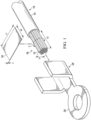
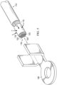
- FIG. 1 illustrates a wire 10 having a conductor 12 and an insulating layer 14 surrounding the conductor 12. A portion of the insulating layer 14 is shown to be removed from the conductor 12 to expose a bare portion 16 of the conductor 12.
- the insulating layer 14 can be removed with any of a variety of suitable methods, such as through interaction with a set of wire strippers.
- any of a variety of suitable alternative conductors can be used having different quantities/sizes of strands, including a conductor having an individual strand (e.g., a solid conductor) and/or being devoid of insulation (e.g., a grounding conductor.
- a conductive foil layer 18 is attached to a portion of the bare portion 16 of the conductor 12.
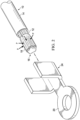
- the conductive foil layer 18 can be wrapped around the bare portion 16 of the conductor 12, as illustrated in FIG. 2 , and pressure can be applied to the conductive foil layer 18 (in the direction of the arrows P).
- the application of pressure to the conductive foil layer 18 can be the result of simply overlying the conductive foil layer 18 onto the bare portion 16 of the conductor 12 (e.g., by grasping the ends of the conductive foil layer 18 and wrapping it around the bare portion 16).
- the desired pressure can be applied by hand, with a tool (e.g., pliers), or any of a variety of other suitable methods.
- the bare portion 16 of the conductor 12 and the conductive foil layer 18 are joined together.
- the bare portion 16 and the conductive foil layer 18 are joined together through welding, such as through ultrasonic welding, for example. Welding the bare portion 16 and the conductive foil layer 18 together can bond the conductive foil layer 18 to the conductor 12 as well as bond the strands of the conductor 12 together to form an amalgamated mass (e.g., a nugget). Welding can also help break apart any oxidation formed on the conductor 12 that might adversely affect the conductivity between the conductor 12 and the conductive foil layer 18. Welding can accordingly enhance the conductivity characteristics between the conductor 12 and the conductive foil layer 18.
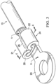
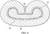
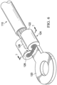
- a terminal 20 is slid over the conductive foil layer 18 and secured to the amalgamated mass of the bare portion 16 and the conductor 12, such as with a crimping tool, for example, to create a terminated wire 21, as illustrated in FIGS. 3 and 4 .
- an exterior surface 22 of a crimping portion 24 of the terminal 20 can be reinforced, such as by applying solder 26 at a separation point 28 of the crimping portion 24, to enhance the durability of the connection between the terminal 20 and the conductor 12.
- the terminal 20 can be nickel plated, or plated with another conductive material, prior to attachment of the terminal 20 to the conductor 12.
- the nickel plating can protect the terminal from galvanic corrosion to enhance the conductivity between the conductor 12 and the material that forms the terminal 20 (e.g., brass).
- the terminated end can additionally or alternatively be dipped in molten solder to enhance durability of the terminated wire 21.
- the terminal 20 is shown to be a ring terminal, it is to be appreciated that any of a variety of suitable alternative contact elements, such as a slotted terminal, a bus bar, or a termination block, for example, can be attached to the wire 10.
- the terminated wire 21 is contemplated for use in a variety of suitable applications, such as, for example, as a vehicular battery cable.
- the conductor 12 and the conductive foil layer 18 are formed of different conductive materials with the conductive foil layer 18 having about the same or higher conductivity than the conductor 12.
- the conductive foil layer 18 can enhance the overall conductivity between the conductor 12 and the terminal 20 as compared to the conductive foil layer 18 not being present (i.e., the conductor 12 and the terminal 20 being entirely in contact with each other).
- the conductor 12 is formed of aluminum or an aluminum alloy
- the conductive foil layer 18 is formed of copper
- the terminal 20 can be formed of brass.
- the copper of the conductive foil layer 18 can allow the interaction between the aluminum conductor 12 and the brass terminal 20 to be more conductive than crimping the brass terminal 20 directly to the aluminum conductor 12 (which in some instances can be non-conductive).
- the conductive foil layer 18 can be formed of a material that is, in examples not according to the present invention, as conductive as or, in embodiments according to the present invention, more conductive than the conductor 12.
- the conductor 12 can be formed of a conductive material having a conductivity of about 3.5*10 7 S/m (at 20 degrees C) or less, and the conductive foil layer 18 can be formed of conductive material having a conductivity of about 4.1*10 7 S/m (at 20 degrees C) or more.
- the conductor 12 can be formed of a conductive material that is substantially susceptible to oxidation, such as an aluminum alloy, a chromium alloy, and/or a magnesium alloy, and the conductive foil layer 18 can be formed of conductive material that is not substantially susceptible to oxidization such as a copper alloy, silver, nickel, and/or gold.
- the conductive foil layer 18 is shown to have a length L1, a width W, and a thickness T and the bare portion 16 of the conductor 12 is shown to have a length L2, a diameter D, and a circumference C.
- the length L1 and width W of the conductive foil layer 18 can be less than the circumference C and the length L2 of the bare portion 16 of the conductor 12, respectively, such that when the conductive foil layer 18 is attached to the conductor 12, the conductive foil layer 18 neither reaches the end of the conductor 12 nor completely surrounds it.
- the length L1 of the conductive foil layer 18 is more than the circumference C of the bare portion 16 of the conductor 12, respectively, such that when the conductive foil layer 18 is attached to the conductor 12, the conductive foil layer 18 overlaps at its ends such that it entirely surrounds the bare portion 16.
- the diameter D of the conductor can be significantly more than the thickness T of the conductive foil layer 18, and can in certain embodiments have a ratio of between about 100:1 and about 500:1 and in certain embodiments can have a ratio of about 200:1.
- the length L1 can be about 40 mm
- the width W can be about 18 mm
- the thickness T can be about 0.035 mm
- the length L2 can be about 20 mm
- the diameter D can be about 8 mm
- the circumference C can be about 25 mm.
- a layer described herein as being a foil, such as conductive foil layer 18, should be understood to mean that the layer is a sheet-like substrate having a length and width that are substantially greater than the thickness of the substrate.
- ratio of the combined length and width of the layer to the thickness of the layer can be between about 500:1 to about 100,000:1. In certain embodiments, the ratio can be about 10,000: 1 to about 25,000: 1 and preferably about 14,000:1
- the bare portion 16 of the conductor 12, alone or in combination with the conductive foil layer 18, can be cleaned before or after application of the conductive foil layer 18 to remove any oxides on the conductor 12 and/or between the conductor 12 and the conductive foil layer thus enhancing the effectiveness of the conductivity between the conductor 12, the conductive foil layer 18, and the terminal 20.
- the conductor 12 and/or conductive foil layer 18 can be cleaned via a plasma treatment performed by a blown-ion air system (not shown). The blown-ion air system can force pressurized air towards an electrode, through a narrow nozzle, and onto the bare portion 16.
- the electrode creates positively charged ions in the pressurized air which is then accelerated by the nozzle and provided onto the bare portion 16 of the conductor 12.
- the positively charged ions in the airstream positively charge the outer surface of the bare portion 16 thereby increasing its surface energy to remove any oxides.
- the conductor 12 and/or conductive foil layer 18 can be cleaned via a high temperature induction heating process that applies a flame to the conductor 12 and/or conductive foil layer 18 using any of a variety of fuels, such as, for example, hydrogen gas, alcohol, and/or acetylene.
- the bare portion 16 of the conductor 12 and the conductive foil layer 18 can be joined by soldering such as by dipping the bare portion 16 and the conductive foil layer 18 together in a molten material (e.g., such as molten tin) or resistance soldering the bare portion 16 and the conductive foil layer 18 together, for example, both of which can enhance the conductivity between the bare portion 16, the conductive foil layer 18, and the terminal 20.
- a molten material e.g., such as molten tin
- resistance soldering the bare portion 16 and the conductive foil layer 18 together for example, both of which can enhance the conductivity between the bare portion 16, the conductive foil layer 18, and the terminal 20.
- cleaning the bare portion 16 and/or the conductive foil layer 18 can encourage the application of solder.
- the soldering can be performed in addition to the welding or in addition to or in lieu of the cleaning described above.
- the bare portion 16 and/or the conductive foil layer 18 can undergo any of a
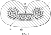
- FIGS. 5-7 illustrate an embodiment which is not according to the present invention and is presented here for illustration purposes only.
- This embodiment relates to a wire 110, a conductive foil layer 118 and a terminal 120 that are similar to, or the same in many respects as, the wire 10, the conductive foil layer 18 and the terminal 120, respectively, illustrated in FIGS. 1-4 .
- the wire 110 can include a conductor 112, an insulating layer 114, a bare portion 116, and a conductive foil layer 118.
- the conductive foil layer 118 can be joined to the bare portion 116 of the conductor 112 by applying pressure to the conductive foil layer 118 (in the direction of the arrows P) and without any welding (ultrasonic or otherwise).
- the terminal 20 can be slid over the bundle of strands (e.g., 123) at the bare portion 16 and secured to the bundle of strands (e.g., 123), such as with a crimping tool, for example.
- An exterior surface 122 of a crimping portion 124 of the terminal 120 can be reinforced, such as by applying solder 126 at a separation point 128 of the crimping portion 124.
- FIG. 8 illustrates a wire 210, a conductive foil layer 218 and a terminal 220 that are similar to, or the same, in many respects as the wire 10, the conductive foil layer 18 and the terminal 20, respectively, illustrated in FIGS. 1-4 .
- the wire 210 can include a conductor 212, an insulating layer 214, and a bare portion 216.
- the conductive foil layer 218, according to this invention, is a corrugated screen having a plurality of elevated portions (e.g., points) distributed along upper and lower surfaces (upper surface 230 shown).
- the points can abrade the bare portion 216 of the conductor 212 (e.g., remove any oxidation) to facilitate effective electrical contact between the bare portion and the conductive foil layer 218. If the bare portion 216 and the conductive foil layer 218 are joined by soldering, as described above, the solder can collect in pockets defined between the points to facilitate effective bonding between the bare portion 216 and the conductive foil layer 218.
- the conductive foil layer 218 can be formed of nickel and the conductor 212 can be formed of aluminum 212.
- FIGS. 9-10 illustrate a wire 310 that is similar to, or the same, in many respects as the wire 10 illustrated in FIGS. 1-4 .
- the wire 310 can include a conductor 312, an insulating layer 314, and a bare portion 316.
- a ferrule 331 can be provided in lieu of, or in addition to, a conductive foil layer (e.g., 18).
- the ferrule 331 can be joined to the bare portion similarly as described above and a terminal (not shown) can then be secured thereto.
- a terminated wire e.g., an alternative terminated wire
- the alternative terminated wire can be similar in many respects to the terminated wire 21 described above except that the alternative terminated wire does not include a conductive foil layer (e.g., 18).
- a portion of an insulating layer e.g., 14
- a conductor e.g., 12
- a bare portion e.g., 16
- the bare portion can then be cleaned (e.g., with a plasma treatment) and welded (e.g., through ultrasonic welding) to bind individual strands of the conductor together.
- the steps of cleaning and welding can be performed in any order. Once welded, the bare portion can be soldered (e.g., through tin dipping or resistive soldering). A terminal (e.g., 20) can then be attached to the bare portion insulating layer to create the alternative terminated wire.
- the conductor 112 can be formed of aluminum and the conductive foil layer can be formed of nickel.
- the terminated wire that was tested was a 0 AWG (1/0) aluminum wire having a bare portion (e.g., 14) measuring about 20 mm, a copper conductive foil layer (e.g., 18) having a length (e.g., L1) of about 40 mm, a width (e.g., W) of about 18 mm, and a thickness (e.g., T) of about 0.035 mm, and a brass terminal.
- the copper conductive foil layer was manually wrapped onto the bare portion and then was ultrasonically welded to form a nugget. A terminal was then crimped onto the nugget.
- Comparative testing was also conducted to compare the results for different terminations of a 0 AWG (1/0) aluminum wire having a bare portion (e.g., 14) measuring about 20 mm, a copper conductive foil layer (e.g., 18) having a length (e.g., L1) of about 40 mm, a width (e.g., W) of about 20 mm, and a thickness (e.g., T) of about 0.035 mm, and a brass terminal.
- a variety of different terminated wires were assembled using certain of the methodologies described above and resistance tests were performed on the terminated wires.
- Example Termination Method Resistance (Ohms)
- Example #1 Bare Conductor with Terminal Crimped Directly to Bare Conductor Open Circuit (high resistance)
- Example #2 Terminated Conductor Prepared and Terminated Without Conductive Foil Layer as follows: 0.345 milliohms 1.
- Ultrasonically Weld Bare Conductor 2.
- Plasma Clean Welded Bare Conductor 3.
- Dip Bare Conductor in Molten Solder 4.
- Crimp Terminal to Soldered End of Bare Conductor. 5.
- Resistance Solder Outer Surface of Terminal Example #3 Terminated Conductor Prepared and Terminated Without Conductive Foil Layer as followss: 0.179 milliohms 1.
- Plasma Clean Bare Conductor 2.
- Ultrasonically Weld Bare Conductor 3. Plasma Clean Bare Conductor 4.
Landscapes
- Engineering & Computer Science (AREA)
- Manufacturing & Machinery (AREA)
- Connections Effected By Soldering, Adhesion, Or Permanent Deformation (AREA)
Claims (15)
- Verfahren zum Anschließen eines Drahtes (10; 210) mit einem Kontaktelement (20; 220), wobei der Draht einen Leiter (12; 212) und eine den Leiter umgebende Isolierschicht (14; 214) umfasst, wobei der Leiter aus Aluminium oder einer Aluminiumlegierung gebildet ist, wobei das Verfahren umfasst:Entfernen der Isolierschicht von dem Leiter, um einen Teil (16; 216) des Leiters freizulegen, wobei der freigelegte Teil einen Umfang aufweist;Anbringen einer leitenden Folienschicht (18; 218) auf dem freigelegten Teil des Leiters, so dass die leitende Folienschicht (18; 218) den Umfang des freigelegten Teils des Leiters vollständig umgibt;Verschweißen der leitenden Folienschicht (18; 218) und des freiliegenden Abschnitts des Leiters miteinander, um eine verschmolzene Masse zu bilden; undAnbringen des Kontaktelements (20; 220) auf der verschmolzenen Masse, wobei das Kontaktelement aus einem anderen Material als der Leiter (12; 212) und die leitende Folienschicht (18; 218) gebildet ist, wobei:
die leitende Folienschicht (18; 218) aus Kupfer gebildet ist, wobei das Verfahren dadurch gekennzeichnet ist, dass die leitende Folienschicht (218) eine gewellte Abschirmung mit einer Vielzahl von erhöhten Abschnitten umfasst, die entlang der oberen und unteren Oberflächen verteilt sind; und wenn die leitende Folienschicht (218) auf dem freiliegenden Abschnitt (216) installiert wird, die erhöhten Abschnitte so konfiguriert sind, dass sie den freiliegenden Abschnitt (216) des Leiters (212) vor dem Verschweißen der leitenden Folienschicht (218) und des freiliegenden Abschnitts abschleifen. - Verfahren nach Anspruch 1, wobei das Anbringen des Kontaktelements (20; 220) auf der verschmolzenen Masse das Crimpen des Kontaktelements umfasst.
- Verfahren nach Anspruch 1 oder 2, wobei das Zusammenschweißen der leitenden Folienschicht (18; 218) und des freiliegenden Abschnitts (16; 216) des Leiters (12; 212) das Ultraschallschweißen der leitenden Folienschicht mit dem freiliegenden Abschnitt des Leiters umfasst.
- Verfahren nach einem der Ansprüche 1 bis 3 umfassend das Reinigen des freiliegenden Abschnitts (16; 216) des Leiters (12; 212) vor dem Zusammenschweißen der leitenden Folienschicht (18; 218) und des freiliegenden Abschnitts des Leiters, und optional umfasst das Reinigen des freiliegenden Abschnitts des Leiters die Plasmabehandlung des freiliegenden Abschnitts des Leiters.
- Verfahren nach einem der Ansprüche 1 bis 4, das ferner das Aufbringen von Lot (26) auf die amalgamierte Masse umfasst, und wobei das Aufbringen von Lot auf die amalgamierte Masse optional das Eintauchen der amalgamierten Masse in ein geschmolzenes Material umfasst.
- Verfahren nach einem der Ansprüche 1 bis 5, wobei das Kontaktelement (20; 220) aus Messing besteht.
- Verfahren nach einem der Ansprüche 1 bis 6, wobei die leitende Folienschicht (18; 218) eine Dicke aufweist und das Verhältnis des Durchmessers des Leiters (12; 212) zur Dicke der leitenden Folienschicht etwa 200:1 beträgt.
- Verfahren nach Anspruch 2 umfasst ferner das Löten einer Außenfläche des Kontaktelements (20; 220).
- Verfahren nach einem der Ansprüche 1 bis 8, wobei das Anbringen der leitenden Folienschicht (18; 218) das vollständige Umwickeln des freiliegenden Abschnitts (16; 216) des Leiters (12; 212) mit der leitenden Folienschicht umfasst, so dass sich gegenüberliegende Enden der leitenden Folienschicht überlappen.
- Anschlussdraht (21), umfassend: einen Leiter (12; 212), wobei der Leiter einen freiliegenden Abschnitt (16; 216) umfasst und aus Aluminium oder einer Aluminiumlegierung gebildet ist, wobei der freiliegende Abschnitt einen Umfang aufweist; eine leitende Folienschicht (18; 218), die aus Kupfer gebildet und auf dem freiliegenden Abschnitt des Leiters so installiert ist, dass die leitende Folienschicht den Umfang des freiliegenden Abschnitts des Leiters vollständig umgibt; ein Kontaktelement (20; 220), das aus einem anderen Material als der Leiter und die leitende Folienschicht gebildet ist; wobei:
die leitende Folienschicht (18; 218) und der freiliegende Abschnitt des Leiters miteinander verschweißt sind, um eine verschmolzene Masse zu bilden; das Kontaktelement (20; 220) an der verschmolzenen Masse befestigt ist, wobei der abgeschlossene Draht dadurch gekennzeichnet ist, dass die leitende Folienschicht (218) eine gewellte Abschirmung mit einer Vielzahl von erhöhten Abschnitten umfasst, die entlang der oberen und unteren Oberflächen verteilt sind; und wenn die leitende Folienschicht (218) auf dem freiliegenden Abschnitt (216) installiert ist, die erhöhten Abschnitte so konfiguriert sind, dass sie den freiliegenden Abschnitt (216) des Leiters (212) vor dem Verschweißen der leitenden Folienschicht (218) und des freiliegenden Abschnitts abschleifen. - Anschlussdraht nach Anspruch 10, wobei der Leiter (12; 212) ein blanker Leiter ist.
- Anschlussdraht nach Anspruch 10 oder 11, wobei der Leiter (12; 212) aus einer Aluminiumlegierung und das Kontaktelement (20; 220) aus Messing besteht.
- Anschlussdraht nach einem der Ansprüche 10-12, wobei die leitende Folienschicht (18; 218) und der freiliegende Teil (16; 216) des Leiters (12; 212) durch Ultraschallschweißen miteinander verbunden sind.
- Anschlussdraht nach einem der Ansprüche 10-13, wobei der Leiter (12; 212) einen Durchmesser hat, die leitende Folienschicht (18; 218) eine Dicke hat und das Verhältnis des Durchmessers des Leiters zur Dicke der leitenden Folienschicht etwa 200:1 beträgt.
- Anschlussdraht nach einem der Ansprüche 10-14, wobei die leitende Folienschicht (18; 218) gegenüberliegende Enden aufweist, die einander überlappen, wenn sie an dem freiliegenden Abschnitt (16; 216) des Leiters (12; 212) angebracht ist.
Applications Claiming Priority (2)
| Application Number | Priority Date | Filing Date | Title |
|---|---|---|---|
| US201462059317P | 2014-10-03 | 2014-10-03 | |
| PCT/US2015/053738 WO2016054516A1 (en) | 2014-10-03 | 2015-10-02 | Wire and methods for preparing a wire to receive a contact element |
Publications (4)
| Publication Number | Publication Date |
|---|---|
| EP3201989A1 EP3201989A1 (de) | 2017-08-09 |
| EP3201989A4 EP3201989A4 (de) | 2018-03-07 |
| EP3201989C0 EP3201989C0 (de) | 2024-09-25 |
| EP3201989B1 true EP3201989B1 (de) | 2024-09-25 |
Family
ID=59253320
Family Applications (1)
| Application Number | Title | Priority Date | Filing Date |
|---|---|---|---|
| EP15847577.2A Active EP3201989B1 (de) | 2014-10-03 | 2015-10-02 | Draht und verfahren zur herstellung eines drahtes zur aufnahme eines kontaktelements |
Country Status (2)
| Country | Link |
|---|---|
| EP (1) | EP3201989B1 (de) |
| CN (1) | CN107004962B (de) |
Families Citing this family (2)
| Publication number | Priority date | Publication date | Assignee | Title |
|---|---|---|---|---|
| JP7041180B2 (ja) * | 2020-02-10 | 2022-03-23 | 矢崎総業株式会社 | 電線の接続構造及び接続方法 |
| CN113054508A (zh) * | 2021-03-12 | 2021-06-29 | 明讯新材料(常州)有限公司 | 一种线缆端子压接方法 |
Citations (1)
| Publication number | Priority date | Publication date | Assignee | Title |
|---|---|---|---|---|
| DE10223397A1 (de) * | 2003-10-04 | 2003-12-24 | Edelhoff Adolf Feindrahtwerk | Verfahren und Verbindung zur Kontaktierung eines Aluminiumkabels |
Family Cites Families (9)
| Publication number | Priority date | Publication date | Assignee | Title |
|---|---|---|---|---|
| US3716909A (en) * | 1972-04-13 | 1973-02-20 | Aluminum Co Of America | Improved method of soldering |
| US5425832A (en) * | 1990-10-05 | 1995-06-20 | Bridgestone Corporation | Surface treatment of fluoropolymer members and preparation of composite products therefrom |
| JP2000299140A (ja) * | 1999-04-15 | 2000-10-24 | Yazaki Corp | 電線と接続端子の接続方法及び接続構造 |
| JP2007305314A (ja) * | 2006-05-08 | 2007-11-22 | Hitachi Cable Ltd | 接続端子付きケーブルとその製造方法、並びに接続端子とケーブルとの超音波溶接方法および超音波溶接機 |
| JP5235369B2 (ja) * | 2007-09-18 | 2013-07-10 | 株式会社オートネットワーク技術研究所 | ワイヤーハーネスおよびその製造方法ならびに絶縁電線の接続方法 |
| JP5447071B2 (ja) * | 2010-03-25 | 2014-03-19 | 株式会社オートネットワーク技術研究所 | 端子金具付き電線及びその製造方法 |
| EP2625746B1 (de) * | 2010-10-06 | 2017-11-01 | Sonics & Materials, Inc. | System und verfahren zur klemmung von aluminiumleitern |
| DE112013002610T5 (de) * | 2012-03-30 | 2015-02-26 | Yazaki Corporation | Gecrimpter Drahtanschluss |
| DE102013201167A1 (de) * | 2013-01-24 | 2014-08-07 | Elringklinger Ag | Verfahren zum Herstellen einer elektrisch leitenden Verbindung zwischen einer elektrischen Leitung und einem elektrisch leitenden Bauteil und nach dem Verfahren hergestellte Baugruppe |
-
2015
- 2015-10-02 EP EP15847577.2A patent/EP3201989B1/de active Active
- 2015-10-02 CN CN201580061388.9A patent/CN107004962B/zh active Active
Patent Citations (1)
| Publication number | Priority date | Publication date | Assignee | Title |
|---|---|---|---|---|
| DE10223397A1 (de) * | 2003-10-04 | 2003-12-24 | Edelhoff Adolf Feindrahtwerk | Verfahren und Verbindung zur Kontaktierung eines Aluminiumkabels |
Also Published As
| Publication number | Publication date |
|---|---|
| EP3201989A4 (de) | 2018-03-07 |
| EP3201989C0 (de) | 2024-09-25 |
| CN107004962B (zh) | 2021-01-26 |
| EP3201989A1 (de) | 2017-08-09 |
| CN107004962A (zh) | 2017-08-01 |
Similar Documents
| Publication | Publication Date | Title |
|---|---|---|
| US9991608B2 (en) | Wire and methods for preparing a wire to receive a contact element | |
| EP2192601B1 (de) | Kabelbaum und verfahren zu seiner herstellung | |
| US20120324727A1 (en) | Crimp connection to aluminum cable | |
| JP4580445B2 (ja) | 端子とそれを用いたコイル装置 | |
| US11362445B2 (en) | Contact system for contacting a braided shield and a contact element | |
| WO2013032030A1 (en) | Electric cable end processing method and electric cable end structure with solder coating and sheath protection | |
| CN105390905B (zh) | 覆皮电线的接合方法 | |
| JP2016001551A (ja) | 被覆電線および圧着端子付き電線 | |
| CN107005014A (zh) | 带端子电线及带端子电线的制造方法 | |
| WO2012161292A1 (en) | Connection structure of crimping connection part of aluminum electric wire and metal terminal and method for manufacturing the same | |
| WO2016017013A1 (ja) | 端子と電線の接合方法および電線接続用の端子 | |
| JP2013020761A (ja) | アルミリッツ線の端子接続方法及び端子接続部 | |
| JP2011124178A (ja) | 端子金具付き電線及びその製造方法 | |
| CN107004962B (zh) | 导线和制备导线以接收接触元件的方法 | |
| WO2018104166A1 (en) | A bimetal end sleeve | |
| JP6941731B2 (ja) | 電気デバイス用の撚り線コネクタ及び撚り線コネクタの製造方法 | |
| WO2015122268A1 (ja) | アルミニウム系電線の端子接続構造 | |
| GB2052891A (en) | Method of attaching a contact element to an electric line | |
| JP6013417B2 (ja) | 被覆電線の接合方法 | |
| KR101282631B1 (ko) | 전선의 단자 접속방법 | |
| JP4894624B2 (ja) | 導線の接続方法 | |
| JP6276820B2 (ja) | 被覆電線の接合方法 | |
| JP2017152094A (ja) | 端子部材 | |
| WO2015064667A1 (ja) | リッツ線用端子 | |
| JP6232368B2 (ja) | 端子の接続方法 |
Legal Events
| Date | Code | Title | Description |
|---|---|---|---|
| STAA | Information on the status of an ep patent application or granted ep patent |
Free format text: STATUS: THE INTERNATIONAL PUBLICATION HAS BEEN MADE |
|
| PUAI | Public reference made under article 153(3) epc to a published international application that has entered the european phase |
Free format text: ORIGINAL CODE: 0009012 |
|
| STAA | Information on the status of an ep patent application or granted ep patent |
Free format text: STATUS: REQUEST FOR EXAMINATION WAS MADE |
|
| 17P | Request for examination filed |
Effective date: 20170331 |
|
| AK | Designated contracting states |
Kind code of ref document: A1 Designated state(s): AL AT BE BG CH CY CZ DE DK EE ES FI FR GB GR HR HU IE IS IT LI LT LU LV MC MK MT NL NO PL PT RO RS SE SI SK SM TR |
|
| AX | Request for extension of the european patent |
Extension state: BA ME |
|
| DAV | Request for validation of the european patent (deleted) | ||
| DAX | Request for extension of the european patent (deleted) | ||
| A4 | Supplementary search report drawn up and despatched |
Effective date: 20180206 |
|
| RIC1 | Information provided on ipc code assigned before grant |
Ipc: H01R 4/02 20060101AFI20180131BHEP Ipc: H01R 4/62 20060101ALI20180131BHEP Ipc: H01R 4/18 20060101ALN20180131BHEP Ipc: H01B 1/02 20060101ALI20180131BHEP Ipc: H01R 43/28 20060101ALI20180131BHEP Ipc: H01R 43/02 20060101ALI20180131BHEP |
|
| STAA | Information on the status of an ep patent application or granted ep patent |
Free format text: STATUS: EXAMINATION IS IN PROGRESS |
|
| 17Q | First examination report despatched |
Effective date: 20180926 |
|
| GRAP | Despatch of communication of intention to grant a patent |
Free format text: ORIGINAL CODE: EPIDOSNIGR1 |
|
| STAA | Information on the status of an ep patent application or granted ep patent |
Free format text: STATUS: GRANT OF PATENT IS INTENDED |
|
| RIC1 | Information provided on ipc code assigned before grant |
Ipc: H01R 4/18 20060101ALN20240418BHEP Ipc: H01R 4/62 20060101ALI20240418BHEP Ipc: H01R 4/02 20060101AFI20240418BHEP Ipc: H01B 1/02 20060101ALI20240418BHEP Ipc: H01R 43/28 20060101ALI20240418BHEP Ipc: H01R 43/02 20060101ALI20240418BHEP |
|
| INTG | Intention to grant announced |
Effective date: 20240502 |
|
| RIC1 | Information provided on ipc code assigned before grant |
Ipc: H01R 4/18 20060101ALN20240419BHEP Ipc: H01B 1/02 20060101ALI20240419BHEP Ipc: H01R 43/28 20060101ALI20240419BHEP Ipc: H01R 43/02 20060101ALI20240419BHEP Ipc: H01R 4/62 20060101ALI20240419BHEP Ipc: H01R 4/02 20060101AFI20240419BHEP |
|
| GRAS | Grant fee paid |
Free format text: ORIGINAL CODE: EPIDOSNIGR3 |
|
| GRAA | (expected) grant |
Free format text: ORIGINAL CODE: 0009210 |
|
| STAA | Information on the status of an ep patent application or granted ep patent |
Free format text: STATUS: THE PATENT HAS BEEN GRANTED |
|
| AK | Designated contracting states |
Kind code of ref document: B1 Designated state(s): AL AT BE BG CH CY CZ DE DK EE ES FI FR GB GR HR HU IE IS IT LI LT LU LV MC MK MT NL NO PL PT RO RS SE SI SK SM TR |
|
| REG | Reference to a national code |
Ref country code: GB Ref legal event code: FG4D |
|
| REG | Reference to a national code |
Ref country code: CH Ref legal event code: EP |
|
| REG | Reference to a national code |
Ref country code: DE Ref legal event code: R096 Ref document number: 602015089994 Country of ref document: DE |
|
| REG | Reference to a national code |
Ref country code: IE Ref legal event code: FG4D |
|
| U01 | Request for unitary effect filed |
Effective date: 20241021 |
|
| U07 | Unitary effect registered |
Designated state(s): AT BE BG DE DK EE FI FR IT LT LU LV MT NL PT RO SE SI Effective date: 20241104 |
|
| U20 | Renewal fee for the european patent with unitary effect paid |
Year of fee payment: 10 Effective date: 20241127 |
|
| PG25 | Lapsed in a contracting state [announced via postgrant information from national office to epo] |
Ref country code: NO Free format text: LAPSE BECAUSE OF FAILURE TO SUBMIT A TRANSLATION OF THE DESCRIPTION OR TO PAY THE FEE WITHIN THE PRESCRIBED TIME-LIMIT Effective date: 20241225 |
|
| PG25 | Lapsed in a contracting state [announced via postgrant information from national office to epo] |
Ref country code: GR Free format text: LAPSE BECAUSE OF FAILURE TO SUBMIT A TRANSLATION OF THE DESCRIPTION OR TO PAY THE FEE WITHIN THE PRESCRIBED TIME-LIMIT Effective date: 20241226 |
|
| PG25 | Lapsed in a contracting state [announced via postgrant information from national office to epo] |
Ref country code: RS Free format text: LAPSE BECAUSE OF FAILURE TO SUBMIT A TRANSLATION OF THE DESCRIPTION OR TO PAY THE FEE WITHIN THE PRESCRIBED TIME-LIMIT Effective date: 20241225 |
|
| PG25 | Lapsed in a contracting state [announced via postgrant information from national office to epo] |
Ref country code: RS Free format text: LAPSE BECAUSE OF FAILURE TO SUBMIT A TRANSLATION OF THE DESCRIPTION OR TO PAY THE FEE WITHIN THE PRESCRIBED TIME-LIMIT Effective date: 20241225 Ref country code: NO Free format text: LAPSE BECAUSE OF FAILURE TO SUBMIT A TRANSLATION OF THE DESCRIPTION OR TO PAY THE FEE WITHIN THE PRESCRIBED TIME-LIMIT Effective date: 20241225 Ref country code: GR Free format text: LAPSE BECAUSE OF FAILURE TO SUBMIT A TRANSLATION OF THE DESCRIPTION OR TO PAY THE FEE WITHIN THE PRESCRIBED TIME-LIMIT Effective date: 20241226 |
|
| PG25 | Lapsed in a contracting state [announced via postgrant information from national office to epo] |
Ref country code: IS Free format text: LAPSE BECAUSE OF FAILURE TO SUBMIT A TRANSLATION OF THE DESCRIPTION OR TO PAY THE FEE WITHIN THE PRESCRIBED TIME-LIMIT Effective date: 20250125 |
|
| PG25 | Lapsed in a contracting state [announced via postgrant information from national office to epo] |
Ref country code: SM Free format text: LAPSE BECAUSE OF FAILURE TO SUBMIT A TRANSLATION OF THE DESCRIPTION OR TO PAY THE FEE WITHIN THE PRESCRIBED TIME-LIMIT Effective date: 20240925 |
|
| PG25 | Lapsed in a contracting state [announced via postgrant information from national office to epo] |
Ref country code: ES Free format text: LAPSE BECAUSE OF FAILURE TO SUBMIT A TRANSLATION OF THE DESCRIPTION OR TO PAY THE FEE WITHIN THE PRESCRIBED TIME-LIMIT Effective date: 20240925 |
|
| PG25 | Lapsed in a contracting state [announced via postgrant information from national office to epo] |
Ref country code: CZ Free format text: LAPSE BECAUSE OF FAILURE TO SUBMIT A TRANSLATION OF THE DESCRIPTION OR TO PAY THE FEE WITHIN THE PRESCRIBED TIME-LIMIT Effective date: 20240925 Ref country code: PL Free format text: LAPSE BECAUSE OF FAILURE TO SUBMIT A TRANSLATION OF THE DESCRIPTION OR TO PAY THE FEE WITHIN THE PRESCRIBED TIME-LIMIT Effective date: 20240925 |
|
| PG25 | Lapsed in a contracting state [announced via postgrant information from national office to epo] |
Ref country code: SK Free format text: LAPSE BECAUSE OF FAILURE TO SUBMIT A TRANSLATION OF THE DESCRIPTION OR TO PAY THE FEE WITHIN THE PRESCRIBED TIME-LIMIT Effective date: 20240925 |
|
| REG | Reference to a national code |
Ref country code: CH Ref legal event code: PL |
|
| PG25 | Lapsed in a contracting state [announced via postgrant information from national office to epo] |
Ref country code: MC Free format text: LAPSE BECAUSE OF FAILURE TO SUBMIT A TRANSLATION OF THE DESCRIPTION OR TO PAY THE FEE WITHIN THE PRESCRIBED TIME-LIMIT Effective date: 20240925 |
|
| PG25 | Lapsed in a contracting state [announced via postgrant information from national office to epo] |
Ref country code: CH Free format text: LAPSE BECAUSE OF NON-PAYMENT OF DUE FEES Effective date: 20241031 |
|
| PLBE | No opposition filed within time limit |
Free format text: ORIGINAL CODE: 0009261 |
|
| STAA | Information on the status of an ep patent application or granted ep patent |
Free format text: STATUS: NO OPPOSITION FILED WITHIN TIME LIMIT |
|
| GBPC | Gb: european patent ceased through non-payment of renewal fee |
Effective date: 20241225 |
|
| 26N | No opposition filed |
Effective date: 20250626 |
|
| PG25 | Lapsed in a contracting state [announced via postgrant information from national office to epo] |
Ref country code: GB Free format text: LAPSE BECAUSE OF NON-PAYMENT OF DUE FEES Effective date: 20241225 |
|
| PG25 | Lapsed in a contracting state [announced via postgrant information from national office to epo] |
Ref country code: IE Free format text: LAPSE BECAUSE OF NON-PAYMENT OF DUE FEES Effective date: 20241002 |
|
| U20 | Renewal fee for the european patent with unitary effect paid |
Year of fee payment: 11 Effective date: 20251027 |
|
| PG25 | Lapsed in a contracting state [announced via postgrant information from national office to epo] |
Ref country code: HR Free format text: LAPSE BECAUSE OF FAILURE TO SUBMIT A TRANSLATION OF THE DESCRIPTION OR TO PAY THE FEE WITHIN THE PRESCRIBED TIME-LIMIT Effective date: 20240925 |
|
| PG25 | Lapsed in a contracting state [announced via postgrant information from national office to epo] |
Ref country code: CY Free format text: LAPSE BECAUSE OF FAILURE TO SUBMIT A TRANSLATION OF THE DESCRIPTION OR TO PAY THE FEE WITHIN THE PRESCRIBED TIME-LIMIT; INVALID AB INITIO Effective date: 20151002 |
|
| PG25 | Lapsed in a contracting state [announced via postgrant information from national office to epo] |
Ref country code: HU Free format text: LAPSE BECAUSE OF FAILURE TO SUBMIT A TRANSLATION OF THE DESCRIPTION OR TO PAY THE FEE WITHIN THE PRESCRIBED TIME-LIMIT; INVALID AB INITIO Effective date: 20151002 |
|
| PG25 | Lapsed in a contracting state [announced via postgrant information from national office to epo] |
Ref country code: TR Free format text: LAPSE BECAUSE OF FAILURE TO SUBMIT A TRANSLATION OF THE DESCRIPTION OR TO PAY THE FEE WITHIN THE PRESCRIBED TIME-LIMIT Effective date: 20240925 |