EP3202040B1 - Näherungssensoranordnung - Google Patents
Näherungssensoranordnung Download PDFInfo
- Publication number
- EP3202040B1 EP3202040B1 EP15781865.9A EP15781865A EP3202040B1 EP 3202040 B1 EP3202040 B1 EP 3202040B1 EP 15781865 A EP15781865 A EP 15781865A EP 3202040 B1 EP3202040 B1 EP 3202040B1
- Authority
- EP
- European Patent Office
- Prior art keywords
- proximity sensor
- sensor assembly
- support
- base
- contact surfaces
- Prior art date
- Legal status (The legal status is an assumption and is not a legal conclusion. Google has not performed a legal analysis and makes no representation as to the accuracy of the status listed.)
- Active
Links
Images


Classifications
-
- B—PERFORMING OPERATIONS; TRANSPORTING
- B25—HAND TOOLS; PORTABLE POWER-DRIVEN TOOLS; MANIPULATORS
- B25J—MANIPULATORS; CHAMBERS PROVIDED WITH MANIPULATION DEVICES
- B25J13/00—Controls for manipulators
- B25J13/08—Controls for manipulators by means of sensing devices, e.g. viewing or touching devices
- B25J13/086—Proximity sensors
-
- B—PERFORMING OPERATIONS; TRANSPORTING
- B25—HAND TOOLS; PORTABLE POWER-DRIVEN TOOLS; MANIPULATORS
- B25J—MANIPULATORS; CHAMBERS PROVIDED WITH MANIPULATION DEVICES
- B25J19/00—Accessories fitted to manipulators, e.g. for monitoring, for viewing; Safety devices combined with or specially adapted for use in connection with manipulators
- B25J19/06—Safety devices
-
- H—ELECTRICITY
- H03—ELECTRONIC CIRCUITRY
- H03K—PULSE TECHNIQUE
- H03K17/00—Electronic switching or gating, i.e. not by contact-making and –breaking
- H03K17/94—Electronic switching or gating, i.e. not by contact-making and –breaking characterised by the way in which the control signals are generated
- H03K17/945—Proximity switches
- H03K17/955—Proximity switches using a capacitive detector
-
- H—ELECTRICITY
- H03—ELECTRONIC CIRCUITRY
- H03K—PULSE TECHNIQUE
- H03K2217/00—Indexing scheme related to electronic switching or gating, i.e. not by contact-making or -breaking covered by H03K17/00
- H03K2217/94—Indexing scheme related to electronic switching or gating, i.e. not by contact-making or -breaking covered by H03K17/00 characterised by the way in which the control signal is generated
- H03K2217/96—Touch switches
- H03K2217/9607—Capacitive touch switches
- H03K2217/960755—Constructional details of capacitive touch and proximity switches
- H03K2217/960765—Details of shielding arrangements
Definitions
- the invention relates to a proximity sensor arrangement for detecting objects approaching the arrangement with a base and a carrier which carries a proximity sensor with a measuring electrode and a shield electrode extending between the measuring electrode and a surface of the base.
- a proximity sensor arrangement is off WO 2013/093 326 A1 and JP 2010 010116 A known.
- Fastening means for fastening the carrier to the base are mentioned in this document, but not described.
- the invention is based on the object of creating a proximity sensor arrangement which is space-saving and robust.
- the object of the invention is achieved by a proximity sensor arrangement with a base such as a robot arm, a board mounted on a surface of the base, carrying contact surfaces and at least one carrier, the contact surfaces complementary to the contact surfaces of the board and at least one proximity sensor connected to the contact surfaces a measuring electrode and a shield electrode extending between the measuring electrode and the surface, the base and the carrier being plug-connected in a plug-in direction parallel to the surface in order to bring the contact surfaces of the circuit board and the carrier into contact.
- a proximity sensor arrangement with a base such as a robot arm, a board mounted on a surface of the base, carrying contact surfaces and at least one carrier, the contact surfaces complementary to the contact surfaces of the board and at least one proximity sensor connected to the contact surfaces a measuring electrode and a shield electrode extending between the measuring electrode and the surface, the base and the carrier being plug-connected in a plug-in direction parallel to the surface in order to bring the contact surfaces of the circuit board and the carrier into contact.
- This connector can be made in different ways. According to a first approach, the carrier itself can be slipped onto the base so that it grips around it in the plug-in state with a friction fit and / or a form fit.
- the plug connection between the base and the carrier can come about indirectly, via the board, in that the contact surfaces are parts of mutually complementary electrical connectors of the carrier and the board.
- a long insertion path can be accommodated in a tightly limited installation space above the surface of the base.
- the height of this installation space can be smaller than the length of the plug-in path.
- the proximity sensor is also electrically contacted by the mechanical plug connection, the assembly effort is minimized.
- a defective proximity sensor can also be easily replaced without any cabling effort by plugging in another carrier with an intact proximity sensor.
- the contact surfaces of the circuit board and the carrier are advantageously aligned or extended in the insertion direction. In this way, an electrical contact can be ensured despite tolerances in the positioning of the carrier.
- one of the contact surfaces can be designed as an electrically conductive spring which is pushed onto a complementary contact surface when the carrier is plugged in and, by being elastically deformed, contributes to the frictional engagement of the plug connection.
- the carrier advantageously has a rigid base plate and the measuring electrode and the shield electrode are arranged on opposite surfaces of the base plate.
- the rigid base plate provides a basis for a holistic fastening of the electrodes and gives the proximity sensor arrangement stability, in particular with respect to the detachment phenomena of the proximity sensors caused by vibrations and oscillations.
- the electrodes can be vapor-deposited, printed or electroplated onto the carrier.
- the base plate can also be used as an insulator that separates the measuring electrode from the shield electrode.
- One of the complementary plug connectors can comprise an edge of the base plate or the circuit board, wherein the contact surfaces can be contact fields arranged on the edge.
- These contact fields can be implemented cost-effectively in the manufacture of the base plate or circuit board using known mass production techniques; there is no need to mount a connector component on the base plate or the circuit board.
- the other connector In order to be able to accommodate the edge, the other connector must overlap with it in a direction perpendicular to the surface of the base, which results in a further minimization of the overhang over the base. If the contact surfaces are attached to the edge of the base plate, the measuring and shield electrodes can be applied over a large area and are applied to the base plate without any interruptions caused by any components.
- One of the contact fields is preferably designed in one piece with the measuring electrode and another in one piece with the shield electrode. In this way, the electrodes and contact fields can be efficiently formed in a single operation.
- the base plate can have projections protruding beyond the surface carrying the shield electrode.
- the projections keep the shield electrode at a distance from the base and prevent the shield electrode and the possibly conductive base from short-circuiting.
- At least one of the protrusions can be a rib running along an edge of the shield electrode.
- the projection can serve as an insulator with respect to a further shield electrode which is adjacent to the first shield electrode and is arranged with it on a common surface.
- the carrier can be secured to the base by at least one screw.
- the screw is preferably oriented transversely to the insertion direction. It cannot cause any movement of the contact surfaces against each other when tightened.
- the carrier is preferably shaped as a channel extending in a longitudinal direction.
- the carrier can at least partially grip the base.
- the shield electrode is on an inside of the channel facing the base and the measuring electrode is on one of the base attached away from the outside of the channel, then the shield electrode can shield the measuring electrode from interference with the base.
- the proximity sensor arrangement preferably has at least two supports, which complement each other to form a shell enclosing the base in a tubular manner. It is thus possible in a simple manner to distribute proximity sensors around the entire circumference of the base in order to detect the approach of foreign bodies from all directions.
- the measuring electrodes and the shield electrodes of the proximity sensors preferably extend in a transverse direction from one edge of the carrier to an opposite edge. In this way, particularly in the case of a tubular arrangement of supports, a uniform sensitivity can be achieved over the entire circumference of this arrangement.
- the point at which an object is approaching cannot be precisely located. Therefore, several proximity sensors should be distributed on the carrier in the longitudinal direction. In this way, the point at which an object is approaching can be recognized using the proximity sensor that responds most strongly to the object.
- multiple contact surfaces can be distributed along the board.
- the circuit board preferably has two groups of contact surfaces, and two carriers are plugged into the base from mutually opposite plugging directions.
- the measuring electrodes of the proximity sensors are preferably designed to be narrower in the longitudinal direction than the shield electrodes. As a result, the measuring electrode can be better shielded by the shield electrode against interference from the base.
- each proximity sensor is limited.
- a further development of the invention therefore provides a switch by means of which several proximity sensors can be connected in parallel.
- the proximity sensors connected in parallel then act like a single proximity sensor; d. H. it is no longer possible to differentiate which of the proximity sensors connected in parallel is approached by an approaching object first.
- this measure has the effect that the range of the detection area of the proximity sensors connected in parallel is extended (compared to proximity sensors not connected in parallel) in order to be able to detect an approaching object from a further distance.
- the parallel connection can be partially or completely canceled by the switch. This reduces the range of the detection range of the proximity sensors again, but from the larger number of available proximity sensors, those to which the object is approaching first can be identified.
- a first preventive measure can be taken. For example, the speed of the robot can be reduced.
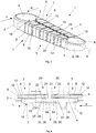
- a carrier 5 is shown.
- the carrier 5 is designed as a channel which extends along a longitudinal direction 6 and has a U-profile in cross section.
- Several proximity sensors 7 are fixedly attached to the carrier 5.
- Each proximity sensor 7 comprises a measuring electrode 8 and a shield electrode 9.
- Measuring and shield electrodes 8 and 9 are firmly connected to the carrier 5 and can, for. B. be glued. In a preferred alternative, the electrodes are electroplated or vapor-deposited onto the carrier 5.
- the measuring electrodes 8 are staggered in the longitudinal direction on an outer side of the channel-shaped carrier 5 and extend in the transverse direction over the entire width of the outer side, from an upper edge 14 to a lower edge 15.
- the shield electrodes 9 are on an inner side of the channel-shaped carrier 5 and also extend over their entire width from edge 14 to edge 15. The carrier 5 is thus almost covered by the measuring and shield electrodes 8 and 9.
- the measuring electrodes 8 are designed to be narrower in the longitudinal direction, so that each shield electrode 9 protrudes laterally beyond the opposite measuring electrode 8 in the longitudinal direction.
- the shield electrodes 9 can also shield the edges of the measuring electrodes 8 from interference fields from the substrate 2.
- the carrier 5 located between the shield electrodes 9.1, 9.2 and measuring electrodes 8.1, 8.2 is formed from an insulating material, typically injection-molded from plastic, and effects an electrical separation of the shield and measuring electrodes.
- the carrier 5 also has a plurality of projections 12 designed as ribs, which extend between the shield electrodes 9 of two adjacent proximity sensors 7. Since the ribs 12 protrude inwards beyond the shield electrodes 9, they keep a cavity 18 open between these and the base 2 and thus ensure galvanic separation of the shield electrodes 9 from the base 2.
- the cavity 18 can be filled with an insulating material.
- the outside of the channel-shaped carrier 5 here has further projections 10 designed as ribs, which protrude outward beyond the measuring electrodes 8.
- the projections 10 are arranged between two proximity sensors 7 and act like an insulator in that they each separate a measuring electrode 8 of the two adjacent proximity sensors 7 from one another. Furthermore, the projections 10 are arranged opposite the projections 12.
- the projections 10 carry a housing 17 which protects the measuring electrodes 8 from direct contact with objects approaching the proximity sensors 7. They hold an air-filled cavity 19 between the measuring electrodes 8 and the housing 17.
- the carrier 5 is flat on its outside, and instead of the housing, a flexible film is attached to the outside to protect the measuring electrodes 8 and glued or welded to the carrier 5 between two adjacent measuring electrodes 8, or a layer of lacquer is applied Measuring electrodes 8 and carrier 5 applied.
- the base 2 can be grounded to divert currents.
- Fig. 3 shows a proximity sensor arrangement 1, which comprises the base 2, here in the form of an arm element 26 of a robot arm, two supports 5 equipped with proximity sensors 7 and a circuit board 4.
- the carriers 5 grip around the base 2 in a frictionally engaged manner, in that one carrier 5 is pushed on from one direction L and the other carrier 5 is pushed on from an opposite direction R until their inner projections 12 lie against the base 2 all around.
- the two channel-shaped supports 5 then complement each other to form a tubular structure and enclose the base 2 extending in the longitudinal direction 6, so that the base 2 is surrounded all around by shield electrodes 9 and measuring electrodes 8 of the proximity sensors 7.
- the circuit board 4 is firmly screwed to a surface 3 of the base 2 with screws 16.
- the circuit board 4 can include all components that are required for signal processing of the proximity sensors 7. In particular, it comprises several pairs of springs 20 for establishing electrical connections with the electrodes 8, 9 on the carriers 5.
- Fig. 4 shows two pairs of springs 20 in an enlarged detail.
- the left pair of springs 20 is used to insert the carrier 5 pushed on in the insertion direction L and the right pair of springs 20 is used to insert the other carrier 5 pushed in the insertion direction R.
- Each pair of springs 20 comprises an upper spring 21 and a lower spring 22 arranged below, which are soldered onto the circuit board 4 and which together delimit an insertion groove.
- the insertion groove of the left pair of springs 20 is open to the left and clamps the upper edge 14 of the left carrier 5 pushed in the insertion direction L.
- the insertion groove of the right pair of springs 20 is open to the right and clamps the upper edge 14 of the right carrier 5 pushed in the insertion direction R.
- the springs 21 and 22 apply a clamping force to the carrier 5 inserted between them, which force the carrier 5 to the circuit board 4 or the pad 2 connected to it frictionally.
- the springs 21 and 22 serve as contact surfaces 35, 37 of the circuit board 4, which can be electrically conductively connected to corresponding contact surfaces 36, 38 of the carrier 5, so that one of the edges 14 has a male connector and the pairs of springs 20 receiving it form complementary female connectors.
- the contact surfaces 36, 38 are arranged in a row along the upper edges 14 of the carrier 5. How Fig. 4 shows, an electrical contact with one of the measuring electrodes 8 of the carrier 5 is made via the upper spring 21 and an electrical contact with one of the shield electrodes 9 of the carrier 5 is made via the lower spring 22. I. E. the measuring and shield electrodes 8, 9 reaching as far as the edge 14 of the carrier 5 are used at the same time as contact surfaces 36, 38 of the carrier 5.
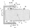
- a carrier 5 which is in a form-fitting connection with the base 2.
- the carrier 5 is pushed onto the base 2 in the insertion direction L.
- a spring 21 is attached to its upper edge 14 and a further spring 22 is attached to its lower edge 15.
- the springs 21 and 22 are two plates 4 which are fastened to the top and bottom of the base 2.
- the boards 4 are congruent and along their to the cutting plane of the Fig. 5 vertical edges are provided with recesses or openings 39. At least one of the circuit boards 4, here the upper circuit board 4, has a contact surface 35 between each opening 39 and the edge adjacent thereto.
- the springs 21 and 22 are shaped like hairpins, each with a leg 40 resting flat on the inside of the carrier and a leg 41 bent in several waves, which are connected in one piece via a bend facing the edge 14.
- a shaft 42 of the bent leg engages when the carrier 5 is pushed in the plug-in direction L up to the stop on the base 2, into one of the openings 39 of the two boards 4 and thereby produces a form fit.
- a second shaft forms a contact surface 36 which, when it snaps into one of the openings 39, also makes electrical contact with the contact surface 35 of the upper board adjacent to the opening 39.
- the shield electrode 9 is in the vicinity of the in Fig. 5
- the spring 21 shown in section is cut out, so that there is no electrical contact between it and this spring 21. Instead, the spring 21 is conductively connected to the measuring electrode 8 arranged on the outside of the carrier 5 via a plated-through hole 43, ie a solder-filled hole in the carrier 5.
- Another feather that is in the perspective of the Fig. 5 is hidden behind the spring 21 shown is soldered directly to the shield electrode 9. Since both electrodes of each proximity sensor 7 are in contact with the upper circuit board 4, there is no need to wire the lower circuit board 4; the spring 22 is only used to fasten the carrier 5.
- the carrier 5 is suitable for retrofitting existing systems with proximity sensors.
- the carriers 5 can be attached and / or screwed to arm elements 26 or 27 of a robot 23.
- the arm members 26 and 27 each serve as a base 2 extending in a longitudinal direction, such as, for. B. in Fig. 3 shown.
- the circuit board 4 is screwed onto a surface of the arm element 26 or 27 serving as a base 2.
- the carrier 5 can then be pushed onto the arm element 26 or 27 and inserted into the spring pairs 20 of the circuit board 4.
- the carriers 5 are each made to match the length of the two arm elements 26 and 27, so that proximity sensors 7 are distributed on both arm elements 26 and 27 over their entire length.
- Fig. 6 outlines of the proximity sensors 7 are indicated with dashed lines.
- the robot 23 can move its arm elements 26 and 27 in different directions.
- the lower arm element 26 is rotatably supported by means of a joint unit 25 with respect to a stationary base 24 about a vertical first axis 31 and a second axis 32 which is perpendicular to the plane of the drawing in the configuration shown here.
- the upper arm element 27 is rotatably supported relative to the lower arm element 26 by means of a further joint unit 25 about a third axis 33 parallel to the second axis and about a fourth axis 34 running in its longitudinal direction.
- an instrument 28 is rotatably mounted relative to the upper arm element 27 by means of a further joint unit 25.
- this proximity sensor 7 If an object 30 comes into the detection area of at least one of the proximity sensors 7 located on the arm elements 26 and 27, this proximity sensor 7 generates a signal and forwards it to a control unit 29, which can be accommodated in the base 24.
- the control unit 29 can then initiate a suitable safety measure to protect against a collision of the robot 23 with the object 30 and, for example, stop a movement of the robot 23.
- Proximity sensors of the two arm elements 26, 27, in particular those in the vicinity of the joint unit 25, can also detect one another if they come close to one another by pivoting about the third axis 33.
- the insertion directions R, L are aligned parallel to the third axis 33, so that the proximity sensors of one of the two supports 5 mounted on the arm element 26 are always facing away from the other arm element 27 and are not disturbed by it.
- control unit 29 can switch the proximity sensors 7 located on the same carrier 5 all or in groups of adjacent proximity sensors 7 in parallel in order to create a composite sensor with a larger electrode area. If an object 30 has been detected by such a composite sensor, the parallel connection can be completely or partially canceled again.
- the range is reduced again as a result, the point of the arm element 26 or 27 which the object 30 is approaching can be localized more precisely, since the proximity sensors which are not connected in parallel can detect objects separately from one another.
Landscapes
- Engineering & Computer Science (AREA)
- Robotics (AREA)
- Mechanical Engineering (AREA)
- Human Computer Interaction (AREA)
- Switches That Are Operated By Magnetic Or Electric Fields (AREA)
- Measurement Of Length, Angles, Or The Like Using Electric Or Magnetic Means (AREA)
Description
- Die Erfindung betrifft eine Näherungssensoranordnung zum Detektieren von sich der Anordnung nähernden Objekten mit einer Unterlage und einem Träger, der einen Näherungssensor mit einer Messelektrode und einer sich zwischen der Messelektrode und einer Oberfläche der Unterlage erstreckenden Schildelektrode trägt. Eine solche Näherungssensoranordnung ist aus
WO 2013/093 326 A1 undJP 2010 010116 A - Der Erfindung liegt die Aufgabe zugrunde, eine Näherungssensoranordnung zu schaffen, die platzsparend und robust ist.
- Die Aufgabe der Erfindung wird gelöst durch eine Näherungssensoranordnung mit einer Unterlage wie etwa einem Roboterarm, einer auf einer Oberfläche der Unterlage montierten, Kontaktflächen tragenden Platine und wenigstens einem Träger, der zu den Kontaktflächen der Platine komplementäre Kontaktflächen und wenigstens einen mit den Kontaktflächen verbundenen Näherungssensor mit einer Messelektrode und einer sich zwischen Messelektrode und Oberfläche erstreckenden Schildelektrode trägt, wobei zum Inkontaktbringen der Kontaktflächen der Platine und des Trägers Unterlage und Träger in einer zu der Oberfläche parallelen Steckrichtung steckverbunden sind.
- Diese Steckverbindung kann auf unterschiedliche Weise hergestellt werden. Einem ersten Ansatz zufolge ist der Träger selber auf die Unterlage aufsteckbar, so dass er sie im steckverbundenen Zustand reib- und/oder formschlüssig umgreift.
- Einem zweiten Ansatz zufolge kann die Steckverbindung zwischen Unterlage und Träger indirekt, über die Platine, zustande kommen, indem die Kontaktflächen Teile von zueinander komplementären elektrischen Steckverbindern des Trägers und der Platine sind.
- In beiden Fällen kann aufgrund der oberflächenparallelen Steckrichtung ein langer Steckweg in einem eng begrenzten Bauraum über der Oberfläche der Unterlage untergebracht werden. Insbesondere kann die Höhe dieses Bauraums kleiner sein als die Länge des Steckweges.
- Da durch die mechanische Steckverbindung der Näherungssensor zugleich auch elektrisch kontaktiert wird, minimiert sich der Montageaufwand.
- Auch kann ein defekter Näherungssensor ganz ohne Verkabelungsaufwand durch Aufstecken eines anderen Trägers mit einem intakten Näherungssensor einfach ausgewechselt werden.
- Die Kontaktflächen der Platine und des Trägers sind vorteilhafterweise in Steckrichtung ausgerichtet oder ausgedehnt. So kann ein elektrischer Kontakt trotz Toleranzen bei der Positionierung des Trägers sichergestellt werden.
- Beispielsweise kann eine der Kontaktflächen als eine elektrisch leitende Feder ausgebildet sein, die sich beim Stecken des Trägers auf eine komplementäre Kontaktfläche aufschiebt und, indem sie sich dabei elastisch verformt, zum Reibschluss der Steckverbindung beiträgt.
- Der Träger weist vorteilhafterweise eine starre Grundplatte auf und die Messelektrode und die Schildelektrode sind an entgegengesetzten Oberflächen der Grundplatte angeordnet.
- Die starre Grundplatte bietet eine Grundlage einer ganzheitlichen Befestigung der Elektroden und verleiht der Näherungssensoranordnung Stabilität, insbesondere gegenüber durch Vibrationen und Schwingungen hervorgerufene Ablöseerscheinungen der Näherungssensoren. Die Elektroden können auf den Träger aufgedampft, aufgedruckt oder aufgalvanisiert sein.
- Die Grundplatte kann darüber hinaus als Isolator genutzt werden, der die Messelektrode von der Schildelektrode trennt.
- Einer der komplementären Steckverbinder kann einen Rand der Grundplatte oder der Platine umfassen, wobei die Kontaktflächen auf dem Rand angeordnete Kontaktfelder sein können. Diese Kontaktfelder sind kostengünstig bei der Fertigung der Grundplatte oder Platine mit bekannten Massenproduktionstechniken realisierbar, die Montage eines Steckverbinderbauteils auf der Grundplatte oder der Platine erübrigt sich. Der andere Steckverbinder muss, um den Rand aufnehmen zu können, mit diesem in zur Oberfläche der Unterlage senkrechter Richtung überlappen, woraus sich eine weitere Minimierung des Überstands über die Unterlage ergibt. Wenn die Kontaktflächen am Rand der Grundplatte angebracht sind, können die Mess- und Schildelektroden großflächig und frei von Unterbrechungen durch etwaige Bauteile auf der Grundplatte aufgebracht werden.
- Vorzugsweise ist jeweils eines der Kontaktfelder einteilig mit der Messelektrode und ein anderes einteilig mit der Schildelektrode ausgebildet. So können die Elektroden und Kontaktfelder rationell in einem einzigen Arbeitsgang ausgebildet werden.
- Die Grundplatte kann über die die Schildelektrode tragende Oberfläche überstehende Vorsprünge aufweisen. Die Vorsprünge halten die Schildelektrode auf Abstand zur Unterlage und verhindern, dass sich die Schildelektrode und die eventuell leitfähige Unterlage kurzschließen können.
- Wenigstens einer der Vorsprünge kann eine entlang einer Kante der Schildelektrode verlaufende Rippe sein. So kann der Vorsprung als Isolator gegenüber einer weiteren Schildelektrode dienen, die zur ersteren Schildelektrode benachbart und mit dieser auf einer gemeinsamen Oberfläche angeordnet ist.
- Der Träger kann an der Unterlage durch wenigstens eine Schraube gesichert sein.
- Eine Bohrung der Grundplatte, die eine solche Schraube aufnehmen kann, verläuft vorzugsweise durch einen der Vorsprünge. So ist sichergestellt, dass beim Festziehen der Schraube die Schildelektrode nicht gegen die Unterlage gedrückt werden kann.
- Die Schraube ist vorzugsweise quer zur Steckrichtung orientiert. So kann sie beim Festziehen keine Bewegung der Kontaktflächen gegeneinander bewirken.
- Der Träger ist vorzugsweise als sich in einer Längsrichtung erstreckende Rinne geformt. Somit kann der Träger die Unterlage zumindest teilweise umgreifen.
- Wird die Schildelektrode an einer der Unterlage zugewandten Innenseite der Rinne und die Messelektrode an einer von der Unterlage abgewandten Außenseite der Rinne angebracht, dann kann die Schildelektrode die Messelektrode vor Störungen der Unterlage abschirmen.
- Vorzugsweise weist die Näherungssensoranordnung zumindest zwei Träger auf, die sich zu einer die Unterlage rohrförmig umschließenden Hülle ergänzen. So ist es auf einfache Weise möglich, Näherungssensoren um den gesamten Umfang der Unterlage zu verteilen, um die Annäherung von Fremdkörpern aus allen Richtungen zu erfassen.
- Die Messelektroden und die Schildelektroden der Näherungssensoren erstrecken sich vorzugsweise in einer Querrichtung von einem Rand des Trägers zu einem gegenüberliegenden Rand. So kann insbesondere bei einer rohrförmigen Anordnung von Trägern eine über den gesamten Umfang dieser Anordnung gleichmäßige Empfindlichkeit erreicht werden.
- Sofern am Träger nur ein einziger Näherungssensor angebracht ist, kann die Stelle, der sich ein Objekt nähert, nicht exakt lokalisiert werden. Daher sollten am Träger in der Längsrichtung mehrere Näherungssensoren verteilt sein. So kann die Stelle, der sich ein Objekt nähert, anhand desjenigen Näherungssensors erkannt werden, der am stärksten auf das Objekt anspricht.
- Zum Kontaktieren der mehreren Näherungssensoren können entlang der Platine mehrere Kontaktflächen verteilt sein.
- Die Platine weist vorzugsweise zwei Gruppen von Kontaktflächen auf, und zwei Träger sind aus einander entgegengesetzten Steckrichtungen mit der Unterlage steckverbunden.
- Vorzugsweise sind die Messelektroden der Näherungssensoren in der Längsrichtung schmaler als die Schildelektroden ausgebildet. Dadurch kann die Messelektrode besser von der Schildelektrode gegen von der Unterlage ausgehende Störungen geschirmt werden.
- Der Erfassungsbereich eines jeden Näherungssensors ist limitiert. Daher sieht eine Weiterbildung der Erfindung einen Schalter vor, durch den mehrere Näherungssensoren parallel geschaltet werden können. Zwar wirken dann die parallel geschalteten Näherungssensoren wie ein einzelner Näherungssensor; d. h. es kann nicht mehr unterschieden werden, welchem der parallel geschalteten Näherungssensoren ein sich näherndes Objekt zuerst nähert. Jedoch bewirkt diese Maßnahme, dass sich die Reichweite des Erfassungsbereichs der parallel geschalteten Näherungssensoren (im Vergleich zu nicht parallel geschalteten Näherungssensoren) erweitert, um ein sich näherndes Objekt schon aus weiterem Abstand erfassen zu können.
- Die Parallelschaltung kann durch den Schalter teilweise oder ganz wieder aufgehoben werden. Dadurch reduziert sich zwar die Reichweite des Erfassungsbereichs der Näherungssensoren wieder, jedoch können aus der größeren Anzahl der verfügbaren Näherungssensoren diejenigen identifiziert werden, denen sich das Objekt zuerst nähert.
- Bei Erfassung eines Objekts kann eine erste Präventivmaßnahme ergriffen werden. Beispielsweise kann die Geschwindigkeit des Roboters reduziert werden.
- Weitere Merkmale und Vorteile der Erfindung ergeben sich aus der nachfolgenden Beschreibung von Ausführungsbeispielen unter Bezugnahme auf die beigefügten Figuren. Es zeigen:
- Fig. 1
- einen Träger mit Näherungssensoren,
- Fig. 2
- eine Schnittansicht einer Näherungssensoranordnung,
- Fig. 3
- eine von zwei Trägern umschlossene Unterlage,
- Fig. 4
- eine detaillierte Ansicht von Steckverbindungen,
- Fig. 5
- einen mit der Unterlage in formschlüssiger Verbindung stehenden Träger und
- Fig. 6
- einen mit den Trägern bestückten Roboter;
- In
Fig. 1 ist ein Träger 5 gezeigt. Der Träger 5 ist als eine sich entlang einer Längsrichtung 6 erstreckende Rinne ausgebildet, die im Querschnitt ein U-Profil aufweist. Am Träger 5 sind mehrere Näherungssensoren 7 fest angebracht. Jeder Näherungssensor 7 umfasst eine Messelektrode 8 und eine Schildelektrode 9. - Mess- und Schildelektroden 8 und 9 sind mit dem Träger 5 fest verbunden und können z. B. aufgeklebt sein. In einer bevorzugten Alternative sind die Elektroden auf den Träger 5 aufgalvanisiert oder aufgedampft.
- Die Messelektroden 8 sind in Längsrichtung gestaffelt an einer Außenseite des rinnenförmigen Trägers 5 angebracht und erstrecken sich in der Querrichtung über die gesamte Breite der Außenseite, von einem oberen Rand 14 bis zu einem unteren Rand 15. Die Schildelektroden 9 sind an einer Innenseite des rinnenförmigen Trägers 5 angebracht und erstrecken sich ebenfalls über deren gesamte Breite von Rand 14 zum Rand 15. Der Träger 5 ist somit nahezu von den Mess- und Schildelektroden 8 und 9 bedeckt.
- Im Vergleich zu den Schildelektroden 9 sind die Messelektroden 8 in Längsrichtung schmaler ausgelegt, so dass jede Schildelektrode 9 in Längsrichtung die ihr gegenüberliegende Messelektrode 8 seitlich überragt. Somit können die Schildelektroden 9 auch die Ränder der Messelektroden 8 gegen Störfelder aus der Unterlage 2 abschirmen.
- Der zwischen den Schildelektroden 9.1, 9.2 und Messelektroden 8.1, 8.2 befindliche Träger 5 ist aus einem Isolationsmaterial gebildet, typischerweise aus Kunststoff spritzgeformt, und bewirkt eine elektrische Trennung von Schild- und Messelektroden.
- Der Träger 5 weist an der Innenseite ferner mehrere als Rippen ausgebildete Vorsprünge 12 auf, die sich zwischen den Schildelektroden 9 zweier benachbarter Näherungssensoren 7 erstrecken. Indem die Rippen 12 über die Schildelektroden 9 nach innen überstehen, halten sie einen Hohlraum 18 zwischen diesen und der Unterlage 2 offen und stellen so eine galvanische Trennung der Schildelektroden 9 von der Unterlage 2 sicher. Optional kann der Hohlraum 18 mit einem Isoliermaterial ausgefüllt werden.
- Die Außenseite des rinnenförmigen Trägers 5 weist hier weitere als Rippen ausgebildete Vorsprünge 10 auf, die über die Messelektroden 8 nach außen überstehen. Die Vorsprünge 10 sind zwischen zwei Näherungssensoren 7 angeordnet und wirken wie ein Isolator, indem sie jeweils eine Messelektrode 8 der beiden benachbarten Näherungssensoren 7 voneinander trennen. Ferner sind die Vorsprünge 10 den Vorsprüngen 12 gegenüberliegend angeordnet.
- Die Vorsprünge 10 tragen ein Gehäuse 17, das die Messelektroden 8 vor einer direkten Kontaktierung mit sich an die Näherungssensoren 7 annähernden Objekten schützt. Sie halten zwischen den Messelektroden 8 und dem Gehäuse 17 einen mit Luft gefüllten Hohlraum 19 offen.
- Einer nicht gezeichneten Variante zufolge ist der Träger 5 an seiner Außenseite eben, und anstelle des Gehäuses ist als Schutz der Messelektroden 8 eine flexible Folie auf die Außenseite aufgezogen und zwischen zwei benachbarten Messelektroden 8 mit dem Träger 5 verklebt oder verschweißt, oder eine Lackschicht ist auf Messelektroden 8 und Träger 5 aufgetragen.
- Durch die Vorsprünge 10 und 12 sind quer zur Längsrichtung 6 des Trägers 5 verlaufende Bohrungen 11 (s.
Fig. 1 ) vorgesehen. Durch die Bohrungen 11 können Schrauben 13 (s.Fig. 2 ) eingeführt werden, um den Träger 5 ggf. zusammen mit dem Gehäuse 17 an der Unterlage 2 zu befestigen. - Zur Ableitung von Strömen kann die Unterlage 2 geerdet sein.
-
Fig. 3 zeigt eine Näherungssensoranordnung 1, die die Unterlage 2, hier in Form eines Armelements 26 eines Roboterarms, zwei mit Näherungssensoren 7 ausgerüstete Träger 5 sowie eine Platine 4 umfasst. Die Träger 5 umgreifen die Unterlage 2 reibschlüssig, indem der eine Träger 5 aus einer Richtung L und der andere Träger 5 aus einer entgegengesetzten Richtung R aufgeschoben wird, bis ihre innenliegenden Vorsprünge 12 ringsum an der Unterlage 2 anliegen. Die beiden rinnenförmigen Träger 5 ergänzen sich dann zu einer rohrförmigen Struktur und umschließen die sich in Längsrichtung 6 erstreckende Unterlage 2, so dass die Unterlage 2 ringsum von Schildelektroden 9 und Messelektroden 8 der Näherungssensoren 7 umgeben ist. - Die Platine 4 ist an einer Oberfläche 3 der Unterlage 2 fest mit Schrauben 16 angeschraubt. Die Platine 4 kann sämtliche Bauelemente umfassen, die zur Signalverarbeitung der Näherungssensoren 7 benötigt werden. Sie umfasst insbesondere mehrere Federpaare 20 zum Herstellen von elektrischen Verbindungen mit den Elektroden 8, 9 auf den Trägern 5.
-
Fig. 4 zeigt zwei Federpaare 20 in einem vergrößert dargestellten Ausschnitt. Das linke Federpaar 20 dient zum Einstecken des in Steckrichtung L aufgeschobenen Trägers 5 und das rechte Federpaar 20 dient zum Einstecken des anderen in Steckrichtung R aufgeschobenen Trägers 5. - Jedes Federpaar 20 umfasst jeweils eine obere Feder 21 und eine darunter angeordnete untere Feder 22, die auf der Platine 4 aufgelötet sind und die gemeinsam eine Einstecknut begrenzen. Die Einstecknut des linken Federpaars 20 ist nach links offen und klemmt den oberen Rand 14 des in Steckrichtung L aufgeschobenen linken Trägers 5. Die Einstecknut des rechten Federpaars 20 ist nach rechts offen und klemmt den oberen Rand 14 des in Steckrichtung R aufgeschobenen rechten Trägers 5.
- Somit bringen die Federn 21 und 22 auf den zwischen sie gesteckten Träger 5 eine Klemmkraft auf, die den Träger 5 mit der Platine 4 bzw. der mit dieser verbundenen Unterlage 2 reibschlüssig verbindet.
- Andererseits dienen die Federn 21 und 22 als Kontaktflächen 35, 37 der Platine 4, die mit korrespondierenden Kontaktflächen 36, 38 der Träger 5 elektrisch leitend verbunden werden können, so dass einer der Ränder 14 jeweils einen männlichen Steckverbinder und die ihn aufnehmenden Federpaare 20 einen dazu komplementären weiblichen Steckverbinder bilden. Die Kontaktflächen 36, 38 sind in einer Reihe entlang der oberen Ränder 14 der Träger 5 angeordnet. Wie
Fig. 4 zeigt, wird über die obere Feder 21 ein elektrischer Kontakt mit einer der Messelektroden 8 des Trägers 5 und über die untere Feder 22 ein elektrischer Kontakt mit einer der Schildelektroden 9 des Trägers 5 hergestellt. D. h. die bis zum Rand 14 des Trägers 5 reichenden Mess- und Schildelektroden 8, 9 werden zugleich als Kontaktflächen 36, 38 des Trägers 5 genutzt. - Als Alternative zu der reibschlüssigen Verbindung zeigt
Fig. 5 einen mit der Unterlage 2 in formschlüssiger Verbindung stehenden Träger 5. Der Träger 5 ist in Steckrichtung L auf die Unterlage 2 aufgesteckt. An der Innenseite des Trägers 5 sind an dessen oberen Rand 14 eine Feder 21 und an dessen unteren Rand 15 eine weitere Feder 22 befestigt. Den Federn 21 und 22 liegen zwei Platinen 4 gegenüber, die an Ober- und Unterseite der Unterlage 2 befestigt sind. - Die Platinen 4 sind deckungsgleich und entlang ihrer zur Schnittebene der
Fig. 5 senkrechten Ränder mit Aussparungen oder Durchbrüchen 39 versehen. Wenigstens eine der Platinen 4, hier die obere Platine 4, weist zwischen jedem Durchbruch 39 und dem dazu benachbarten Rand eine Kontaktfläche 35 auf. - Die Federn 21 und 22 sind haarnadelartig geformt, mit jeweils einem an der Innenseite des Trägers flach anliegenden Schenkel 40 und einem in mehreren Wellen gebogenen Schenkel 41, die über einen dem Rand 14 zugewandte Biegung einteilig zusammenhängen. Eine Welle 42 des gebogenen Schenkels rastet, wenn der Träger 5 in der Steckrichtung L bis zum Anschlag auf die Unterlage 2 aufgeschoben ist, in einen der Durchbrüche 39 der beiden Platinen 4 ein und stellt dadurch einen Formschluss her. Eine zweite Welle bildet eine Kontaktfläche 36, die beim Einrasten in einen der Durchbrüche 39 auch einen elektrischen Kontakt zur dem Durchbruch 39 benachbarten Kontaktfläche 35 der oberen Platine herstellt.
- Die Schildelektrode 9 ist in der Umgebung der in
Fig. 5 im Schnitt gezeigten Feder 21 ausgespart, so dass zwischen ihr und dieser Feder 21 kein elektrischer Kontakt besteht. Stattdessen ist die Feder 21 über eine Durchkontaktierung 43, d.h. eine lotgefüllte Bohrung des Trägers 5, mit der außen am Träger 5 angeordneten Messelektrode 8 leitend verbunden. Eine weitere Feder, die in der Perspektive derFig. 5 hinter der gezeigten Feder 21 verborgen ist, ist direkt auf die Schildelektrode 9 aufgelötet. Da somit beide Elektroden jedes Näherungssensors 7 mit der oberen Platine 4 kontaktiert sind, kann auf eine Verdrahtung der unteren Platine 4 verzichtet werden; die Feder 22 dient lediglich der Befestigung des Trägers 5. - Der erfindungsgemäße Träger 5 ist geeignet, bestehende Systeme nachträglich mit Näherungssensoren auszurüsten. Wie in
Fig. 6 gezeigt, können die Träger 5 an Armelemente 26 oder 27 eines Roboters 23 aufgesteckt und/oder angeschraubt werden. Die Armelemente 26 und 27 dienen jeweils als eine sich in eine Längsrichtung erstreckende Unterlage 2, wie z. B. inFig. 3 gezeigt. Die Platine 4 wird auf eine Oberfläche des als Unterlage 2 dienenden Armelements 26 bzw. 27 angeschraubt. Anschließend können die Träger 5 auf das Armelement 26 bzw. 27 aufgeschoben und in die Federpaare 20 der Platine 4 gesteckt werden. - Die Träger 5 sind jeweils angepasst auf die Länge der beiden Armelemente 26 und 27 angefertigt, so dass Näherungssensoren 7 an beiden Armelemente 26 und 27 über deren gesamte Länge verteilt sind. In
Fig. 6 sind Umrisse der Näherungssensoren 7 mit gestrichelten, Linien angedeutet. - Der Roboter 23 kann seine Armelemente 26 und 27 in verschiedene Richtungen bewegen. Das untere Armelement 26 ist mittels einer Gelenkeinheit 25 gegenüber einem feststehenden Sockel 24 um eine vertikale erste Achse 31 und eine in der hier gezeigten Konfiguration zur Zeichnungsebene senkrechte zweite Achse 32 drehbar gelagert. Das obere Armelement 27 ist gegenüber dem unteren Armelement 26 mittels einer weiteren Gelenkeinheit 25 um eine zur zweiten Achse parallele dritte Achse 33 und um eine in seiner Längsrichtung verlaufende vierte Achse 34 drehbar gelagert. Ferner ist ein Instrument 28 mittels einer weiteren Gelenkeinheit 25 gegenüber dem oberen Armelement 27 drehbar gelagert.
- Gerät ein Objekt 30 in den Erfassungsbereich zumindest eines der an den Armelementen 26 und 27 befindlichen Näherungssensoren 7, erzeugt dieser Näherungssensor 7 ein Signal und leitet dieses an eine Steuereinheit 29, die im Sockel 24 untergebracht sein kann. Die Steuereinheit 29 kann daraufhin eine geeignete Sicherheitsmaßnahme zum Schutz vor einer Kollision des Roboters 23 mit dem Objekt 30 einleiten und beispielsweise eine Bewegung des Roboters 23 stoppen.
- Näherungssensoren der beiden Armelemente 26, 27, insbesondere solche in der Nähe der Gelenkeinheit 25 können einander auch gegenseitig erfassen, wenn sie einander durch Schwenken um die dritte Achse 33 nahekommen. Wenigstens am Armelement 26 sind die Steckrichtungen R, L parallel zur dritten Achse 33 ausgerichtet, so dass stets die Näherungssensoren eines der beiden am Armelement 26 montierten Träger 5 vom anderen Armelement 27 abgewandt sind und durch dieses nicht gestört werden.
- Um die Reichweite des Erfassungsbereichs der Näherungssensoranordnung 1 zu erhöhen, kann die Steuereinheit 29 die an einem gleichen Träger 5 befindlichen Näherungssensoren 7 allesamt oder in Gruppen von jeweils einander benachbarten Näherungssensoren 7 parallel schalten, um einen zusammengesetzten Sensor mit größerer Elektrodenfläche zu schaffen. Wurde ein Objekt 30 von einem solchen zusammengesetzten Sensor erfasst, kann die Parallelschaltung vollständig oder in Teilen wieder aufgehoben werden.
- Zwar wird dadurch die Reichweite wieder reduziert, jedoch kann die Stelle des Armelements 26 oder 27, der sich das Objekt 30 annähert, präziser lokalisiert werden, da die nicht parallel geschalteten Näherungssensoren Objekte voneinander losgelöst erkennen können.
-
- 1
- Näherungssensoranordnung
- 2
- Unterlage
- 3
- Oberfläche
- 4
- Platine
- 5
- Träger
- 6
- Längsrichtung
- 7
- Näherungssensor
- 8
- Messelektrode
- 9
- Schildelektrode
- 10
- Vorsprung
- 11
- Bohrung
- 12
- Vorsprung
- 13
- Schraube
- 14
- Rand
- 15
- Rand
- 16
- Schraube
- 17
- Gehäuse
- 18
- Hohlraum
- 19
- Hohlraum
- 20
- Federpaar
- 21
- Feder
- 22
- Feder
- 23
- Roboter
- 24
- Sockel
- 25
- Gelenkeinheit
- 26
- Armelement
- 27
- Armelement
- 28
- Instrument
- 29
- Steuereinheit
- 30
- Objekt
- 31
- Achse
- 32
- Achse
- 33
- Achse
- 34
- Achse
- 35
- Kontaktfläche
- 36
- Kontaktfläche
- 37
- Kontaktfläche
- 38
- Kontaktfläche
- 39
- Durchbruch
- 40
- Schenkel
- 41
- Schenkel
- 42
- Welle
Claims (18)
- Näherungssensoranordnung (1) mit einer Unterlage (2), und wenigstens einem Träger (5), der wenigstens einen Näherungssensor (7) mit einer Messelektrode (8) und einer sich zwischen der Messelektrode (8) und einer Oberfläche (3) erstreckenden Schildelektrode (9) trägt, dadurch gekennzeichnet, dass eine Kontaktflächen (35, 37) tragende Platine (4) auf der Oberfläche (3) der Unterlage (2) montiert ist, dass der Träger (5) zu den Kontaktflächen (35, 37) der Platine (4) komplementäre Kontaktflächen (36, 38) aufweist, dass zum elektrischen Inkontaktbringen der Kontaktflächen (35, 36, 37, 38) der Platine (4) und des Trägers (5) die Unterlage (2) und der Träger (5) in einer zu der Oberfläche (3) parallelen Steckrichtung (R, L) steckverbunden sind, und dass die Mess- und Schildelektroden (8, 9) mit den Kontaktflächen (36, 38) des Trägers (5) elektrisch verbunden sind.
- Näherungssensoranordnung (1) nach Anspruch 1, dadurch gekennzeichnet, dass die Kontaktflächen (35, 36, 37, 38) der Platine (4) und des Trägers (5) in der Steckrichtung (L, R) ausgedehnt sind.
- Näherungssensoranordnung (1) nach Anspruch 1 oder 2, dadurch gekennzeichnet, dass der Träger (5) die Unterlage (2) reib- und/oder formschlüssig umgreift.
- Näherungssensoranordnung (1) nach einem der vorhergehenden Ansprüche, dadurch gekennzeichnet, dass die Kontaktflächen (35, 36, 37, 38) Teile von zueinander komplementären elektrischen Steckverbindern des Trägers (5) und der Platine (4) sind, die die Steckverbindung zwischen Unterlage (2) und Träger (5) vermitteln.
- Näherungssensoranordnung (1) nach Anspruch 3 oder 4, dadurch gekennzeichnet, dass der Träger (5) eine starre Grundplatte aufweist und die Messelektrode (8) und die Schildelektrode (9) an entgegengesetzten Oberflächen der Grundplatte angeordnet sind.
- Näherungssensoranordnung (1) nach Anspruch 5, soweit auf Anspruch 4 rückbezogen, dadurch gekennzeichnet, dass einer der komplementären Steckverbinder einen Rand (14) der Grundplatte oder der Platine (4) umfasst und die Kontaktflächen (35, 36, 37, 38) auf dem Rand (14) angeordnete Kontaktfelder sind.
- Näherungssensoranordnung (1) nach Anspruch 6, dadurch gekennzeichnet, dass jeweils eines der Kontaktfelder einteilig mit der Messelektrode (8) und ein anderes einteilig mit der Schildelektrode (9) ausgebildet ist.
- Näherungssensoranordnung (1) nach Anspruch 6 oder 7, dadurch gekennzeichnet, dass die Grundplatte über die die Schildelektrode (9) tragende Oberfläche überstehende Vorsprünge (12) aufweist.
- Näherungssensoranordnung (1) nach Anspruch 8, dadurch gekennzeichnet, dass wenigstens einer der Vorsprünge (12) eine entlang einer Kante der Schildelektrode (9) verlaufende Rippe ist.
- Näherungssensoranordnung (1) nach Anspruch 8 oder 9, dadurch gekennzeichnet, dass eine die Grundplatte kreuzende Bohrung (11) durch wenigstens einen der Vorsprünge (12) verläuft.
- Näherungssensoranordnung (1) nach einem der vorhergehenden Ansprüche, dadurch gekennzeichnet, dass der Träger (5) an der Platine (4) durch wenigstens eine quer zur Steckrichtung (L, R) orientierte Schraube (13) gesichert ist.
- Näherungssensoranordnung (1) nach einem der vorhergehenden Ansprüche, dadurch gekennzeichnet, dass der Träger (5) als sich in einer Längsrichtung (6) erstreckende Rinne geformt ist.
- Näherungssensoranordnung (1) nach Anspruch 12, dadurch gekennzeichnet, dass zwei Träger (5) sich zu einer die Unterlage (2) rohrförmig umschließenden Hülle ergänzen.
- Näherungssensoranordnung (1) nach einem der Ansprüche 12 bis 13, dadurch gekennzeichnet, dass die Messelektrode (8) und Schildelektrode (9) des Näherungssensors (7) sich in einer Querrichtung von einem Rand (14) des Trägers (5) zu einem gegenüberliegenden Rand (15) erstrecken.
- Näherungssensoranordnung (1) nach einem der vorhergehenden Ansprüche, dadurch gekennzeichnet, dass mehrere Näherungssensoren (7) am Träger (5) in einer Längsrichtung (6) verteilt sind.
- Näherungssensoranordnung (1) nach Anspruch 15, dadurch gekennzeichnet, dass Kontaktflächen (35, 37) zum Kontaktieren der mehreren Näherungssensoren (7) entlang der Platine verteilt sind.
- Näherungssensoranordnung (1) nach Anspruch 15, dadurch gekennzeichnet, dass die Platine (4) zwei Gruppen von Kontaktflächen (35, 37) aufweist und dass zwei Träger (5) aus einander entgegengesetzten Steckrichtungen (L, R) mit der Unterlage (2) steckverbunden sind.
- Näherungssensoranordnung (1) nach einem der Ansprüche 12 bis 17, dadurch gekennzeichnet, dass die Messelektroden (8) der Näherungssensoren (7) in der Längsrichtung (6) schmaler als die Schildelektroden (9) sind.
Applications Claiming Priority (2)
| Application Number | Priority Date | Filing Date | Title |
|---|---|---|---|
| DE102014014050.4A DE102014014050B4 (de) | 2014-09-29 | 2014-09-29 | Näherungssensoranordnung |
| PCT/EP2015/001903 WO2016050344A1 (de) | 2014-09-29 | 2015-09-24 | Näherungssensoranordnung |
Publications (2)
| Publication Number | Publication Date |
|---|---|
| EP3202040A1 EP3202040A1 (de) | 2017-08-09 |
| EP3202040B1 true EP3202040B1 (de) | 2021-04-07 |
Family
ID=54337231
Family Applications (1)
| Application Number | Title | Priority Date | Filing Date |
|---|---|---|---|
| EP15781865.9A Active EP3202040B1 (de) | 2014-09-29 | 2015-09-24 | Näherungssensoranordnung |
Country Status (5)
| Country | Link |
|---|---|
| US (1) | US10335955B2 (de) |
| EP (1) | EP3202040B1 (de) |
| CN (1) | CN107000214B (de) |
| DE (1) | DE102014014050B4 (de) |
| WO (1) | WO2016050344A1 (de) |
Families Citing this family (11)
| Publication number | Priority date | Publication date | Assignee | Title |
|---|---|---|---|---|
| DE112017001677T5 (de) * | 2016-03-29 | 2018-12-13 | Life Robotics Inc. | Näherungssensorvorrichtung und Roboterarmmechanismus |
| FR3070022B1 (fr) * | 2017-08-10 | 2020-11-06 | Fogale Nanotech | Element d’habillage capacitif pour robot, robot muni d’un tel element d’habillage |
| FR3072176B1 (fr) * | 2017-10-10 | 2022-03-04 | Fogale Nanotech | Dispositif de mesure d'impedance |
| JP7052308B2 (ja) * | 2017-11-15 | 2022-04-12 | セイコーエプソン株式会社 | センサー、およびロボット |
| JP7000992B2 (ja) * | 2018-05-25 | 2022-01-19 | トヨタ自動車株式会社 | マニピュレータおよび移動ロボット |
| EP3851256A4 (de) * | 2018-09-14 | 2022-06-01 | Alps Alpine Co., Ltd. | Näherungsdetektionssystem |
| CN109382850B (zh) * | 2018-11-27 | 2024-03-29 | 中国科学院合肥物质科学研究院 | 一种铝合金型材送料机械手防撞系统 |
| JP7311343B2 (ja) * | 2019-07-19 | 2023-07-19 | ファナック株式会社 | ロボット |
| CN112512752A (zh) * | 2019-08-02 | 2021-03-16 | 深圳市越疆科技有限公司 | 装置的避障方法、装置和控制器 |
| CN113451791B (zh) * | 2021-05-22 | 2024-01-05 | 深圳市越疆科技股份有限公司 | 检测电路板与电极的连接结构、电子皮肤、外壳及机械臂 |
| WO2024022585A1 (en) | 2022-07-27 | 2024-02-01 | Abb Schweiz Ag | Robot system with accessories magnetically attached to the robot arm |
Citations (3)
| Publication number | Priority date | Publication date | Assignee | Title |
|---|---|---|---|---|
| JPS63238502A (ja) * | 1987-03-27 | 1988-10-04 | Yokohama Rubber Co Ltd:The | 近接覚・触覚センサ |
| DE20004404U1 (de) * | 2000-03-09 | 2001-07-19 | Merten GmbH & Co. KG, 51674 Wiehl | Elektrischer Installationsschalter |
| JP2010010116A (ja) * | 2008-05-30 | 2010-01-14 | Fujikura Ltd | 接近制御装置および接近センサ |
Family Cites Families (11)
| Publication number | Priority date | Publication date | Assignee | Title |
|---|---|---|---|---|
| US5166679A (en) | 1991-06-06 | 1992-11-24 | The United States Of America As Represented By The Administrator Of The National Aeronautics & Space Administration | Driven shielding capacitive proximity sensor |
| US5539292A (en) * | 1994-11-28 | 1996-07-23 | The United States Of America As Represented By The Administrator Of The National Aeronautics And Space Administration | Capaciflector-guided mechanisms |
| JP2001005126A (ja) | 1999-04-22 | 2001-01-12 | Minolta Co Ltd | 画像形成装置 |
| JP2001057126A (ja) * | 1999-08-16 | 2001-02-27 | San Miyuuron:Kk | タッチスイッチ |
| CN100518654C (zh) * | 2004-08-31 | 2009-07-29 | 皇家飞利浦电子股份有限公司 | X光机的接近传感器 |
| JP4774055B2 (ja) | 2004-08-31 | 2011-09-14 | コーニンクレッカ フィリップス エレクトロニクス エヌ ヴィ | X線装置用の近接センサ |
| DE102005003492B4 (de) | 2005-01-25 | 2008-05-29 | Sick Ag | Sensorsystem und Sicherungsverfahren |
| FI20105368A0 (fi) | 2010-04-09 | 2010-04-09 | Zenrobotics Oy | Herkkä mutta kestävä tuntoaisti |
| DE102011078077A1 (de) * | 2011-06-24 | 2012-12-27 | Ident Technology Ag | Leiterplatte mit Elektrodenkonfiguration eines kapazitiven Sensors |
| FR2985048B1 (fr) * | 2011-12-21 | 2014-08-15 | Nanotec Solution | Dispositif et procede de mesure capacitive sensible a la pression pour interfaces tactiles et sans contact |
| US9896045B2 (en) | 2012-03-15 | 2018-02-20 | Carling Technologies, Inc. | Touch activated, wireless switches |
-
2014
- 2014-09-29 DE DE102014014050.4A patent/DE102014014050B4/de not_active Expired - Fee Related
-
2015
- 2015-09-24 CN CN201580052326.1A patent/CN107000214B/zh not_active Expired - Fee Related
- 2015-09-24 US US15/514,964 patent/US10335955B2/en active Active
- 2015-09-24 EP EP15781865.9A patent/EP3202040B1/de active Active
- 2015-09-24 WO PCT/EP2015/001903 patent/WO2016050344A1/de not_active Ceased
Patent Citations (3)
| Publication number | Priority date | Publication date | Assignee | Title |
|---|---|---|---|---|
| JPS63238502A (ja) * | 1987-03-27 | 1988-10-04 | Yokohama Rubber Co Ltd:The | 近接覚・触覚センサ |
| DE20004404U1 (de) * | 2000-03-09 | 2001-07-19 | Merten GmbH & Co. KG, 51674 Wiehl | Elektrischer Installationsschalter |
| JP2010010116A (ja) * | 2008-05-30 | 2010-01-14 | Fujikura Ltd | 接近制御装置および接近センサ |
Also Published As
| Publication number | Publication date |
|---|---|
| CN107000214A (zh) | 2017-08-01 |
| EP3202040A1 (de) | 2017-08-09 |
| US10335955B2 (en) | 2019-07-02 |
| DE102014014050A1 (de) | 2016-03-31 |
| DE102014014050B4 (de) | 2017-08-03 |
| WO2016050344A1 (de) | 2016-04-07 |
| CN107000214B (zh) | 2019-11-19 |
| US20180236667A1 (en) | 2018-08-23 |
Similar Documents
| Publication | Publication Date | Title |
|---|---|---|
| EP3202040B1 (de) | Näherungssensoranordnung | |
| DE112016001330B4 (de) | Elektrischer Verteiler | |
| DE69631980T2 (de) | Elektrischer Verbinder | |
| EP2112716A2 (de) | Kontaktelement für eine Anschlussklemme, Anschlussklemme und Steckbrücke für ein Kontaktelement | |
| DE102011119842B4 (de) | Elektrisches Verbindungselement und Leiterplattenanordnung | |
| WO2018006892A1 (de) | Anordnung und verfahren zur masseanbindung einer leiterkarte an ein gehäuse eines elektrischen gerätes | |
| DE202015106042U1 (de) | Leiterplatte | |
| EP1555865B1 (de) | Montage einer Sperrkreisanordnung mit diskreten, passiven elektronischen Bauteilen | |
| EP3232454A1 (de) | Busbar mit einer mehrzahl von filmkondensatoren | |
| DE202012002352U1 (de) | Anordnung aus Steckverbinder und Leiterplatte | |
| DE102015115819A1 (de) | Leiterbrückenelement sowie Bestückungsgurt und Leiterplatten mit einem solchen | |
| DE202015008007U1 (de) | Leiterplattenanordnung | |
| DE102004037629B4 (de) | Verbindungselement für Leiterplatten | |
| EP3192155B1 (de) | Elektromotor mit smd-bauteilen und zugehöriges verbindungsteil | |
| EP0249646B1 (de) | Leiterplattenanschlussklemme | |
| EP0078481B1 (de) | Kontaktierungsvorrichtung mit einem Klemmelement zum Kontaktieren von elektrischen Kontaktstellen auf Leiterplatten | |
| DE102009053206B4 (de) | Kontaktelementanordnung | |
| DE102016224657A1 (de) | Verfahren zum Verbinden eines Bauelementträgers mit einer Leiterplatte und Verbund aus einer Leiterplatte und einem Bauelementträger | |
| DE102017011113B4 (de) | Elektrisches Verbindungselement mit einer Stromschiene | |
| WO2003009427A1 (de) | System und verfahren zur elektrischen kontaktierung und mechanischen befestigung von leiterplatten | |
| EP2482386A1 (de) | Vorrichtung zur elektrischen und mechanischen Verbindung von zwei übereinander angeordneten Leiterplatten | |
| DE102014117536A1 (de) | Sensor mit zwei im Winkel verbundenen Leiterplatten und Verfahren zur seitlichen Verbindung zweier Leiterplatten | |
| DE102017105470B4 (de) | Leuchtenbaugruppe | |
| DE102014103040B4 (de) | Leiterplattenanordnung mit flexiblem Verbindungselement | |
| EP0966777B1 (de) | Elektrische baugruppe |
Legal Events
| Date | Code | Title | Description |
|---|---|---|---|
| STAA | Information on the status of an ep patent application or granted ep patent |
Free format text: STATUS: THE INTERNATIONAL PUBLICATION HAS BEEN MADE |
|
| PUAI | Public reference made under article 153(3) epc to a published international application that has entered the european phase |
Free format text: ORIGINAL CODE: 0009012 |
|
| STAA | Information on the status of an ep patent application or granted ep patent |
Free format text: STATUS: REQUEST FOR EXAMINATION WAS MADE |
|
| 17P | Request for examination filed |
Effective date: 20170427 |
|
| AK | Designated contracting states |
Kind code of ref document: A1 Designated state(s): AL AT BE BG CH CY CZ DE DK EE ES FI FR GB GR HR HU IE IS IT LI LT LU LV MC MK MT NL NO PL PT RO RS SE SI SK SM TR |
|
| AX | Request for extension of the european patent |
Extension state: BA ME |
|
| DAV | Request for validation of the european patent (deleted) | ||
| DAX | Request for extension of the european patent (deleted) | ||
| RAP1 | Party data changed (applicant data changed or rights of an application transferred) |
Owner name: ABB SCHWEIZ AG |
|
| GRAP | Despatch of communication of intention to grant a patent |
Free format text: ORIGINAL CODE: EPIDOSNIGR1 |
|
| STAA | Information on the status of an ep patent application or granted ep patent |
Free format text: STATUS: GRANT OF PATENT IS INTENDED |
|
| INTG | Intention to grant announced |
Effective date: 20200916 |
|
| GRAS | Grant fee paid |
Free format text: ORIGINAL CODE: EPIDOSNIGR3 |
|
| GRAJ | Information related to disapproval of communication of intention to grant by the applicant or resumption of examination proceedings by the epo deleted |
Free format text: ORIGINAL CODE: EPIDOSDIGR1 |
|
| GRAL | Information related to payment of fee for publishing/printing deleted |
Free format text: ORIGINAL CODE: EPIDOSDIGR3 |
|
| STAA | Information on the status of an ep patent application or granted ep patent |
Free format text: STATUS: REQUEST FOR EXAMINATION WAS MADE |
|
| GRAP | Despatch of communication of intention to grant a patent |
Free format text: ORIGINAL CODE: EPIDOSNIGR1 |
|
| STAA | Information on the status of an ep patent application or granted ep patent |
Free format text: STATUS: GRANT OF PATENT IS INTENDED |
|
| INTC | Intention to grant announced (deleted) | ||
| INTG | Intention to grant announced |
Effective date: 20210129 |
|
| GRAA | (expected) grant |
Free format text: ORIGINAL CODE: 0009210 |
|
| STAA | Information on the status of an ep patent application or granted ep patent |
Free format text: STATUS: THE PATENT HAS BEEN GRANTED |
|
| AK | Designated contracting states |
Kind code of ref document: B1 Designated state(s): AL AT BE BG CH CY CZ DE DK EE ES FI FR GB GR HR HU IE IS IT LI LT LU LV MC MK MT NL NO PL PT RO RS SE SI SK SM TR |
|
| REG | Reference to a national code |
Ref country code: GB Ref legal event code: FG4D Free format text: NOT ENGLISH |
|
| REG | Reference to a national code |
Ref country code: AT Ref legal event code: REF Ref document number: 1380997 Country of ref document: AT Kind code of ref document: T Effective date: 20210415 Ref country code: CH Ref legal event code: EP |
|
| REG | Reference to a national code |
Ref country code: DE Ref legal event code: R096 Ref document number: 502015014527 Country of ref document: DE |
|
| REG | Reference to a national code |
Ref country code: IE Ref legal event code: FG4D Free format text: LANGUAGE OF EP DOCUMENT: GERMAN |
|
| REG | Reference to a national code |
Ref country code: LT Ref legal event code: MG9D |
|
| REG | Reference to a national code |
Ref country code: NL Ref legal event code: MP Effective date: 20210407 |
|
| PG25 | Lapsed in a contracting state [announced via postgrant information from national office to epo] |
Ref country code: LT Free format text: LAPSE BECAUSE OF FAILURE TO SUBMIT A TRANSLATION OF THE DESCRIPTION OR TO PAY THE FEE WITHIN THE PRESCRIBED TIME-LIMIT Effective date: 20210407 Ref country code: NL Free format text: LAPSE BECAUSE OF FAILURE TO SUBMIT A TRANSLATION OF THE DESCRIPTION OR TO PAY THE FEE WITHIN THE PRESCRIBED TIME-LIMIT Effective date: 20210407 Ref country code: FI Free format text: LAPSE BECAUSE OF FAILURE TO SUBMIT A TRANSLATION OF THE DESCRIPTION OR TO PAY THE FEE WITHIN THE PRESCRIBED TIME-LIMIT Effective date: 20210407 Ref country code: HR Free format text: LAPSE BECAUSE OF FAILURE TO SUBMIT A TRANSLATION OF THE DESCRIPTION OR TO PAY THE FEE WITHIN THE PRESCRIBED TIME-LIMIT Effective date: 20210407 Ref country code: BG Free format text: LAPSE BECAUSE OF FAILURE TO SUBMIT A TRANSLATION OF THE DESCRIPTION OR TO PAY THE FEE WITHIN THE PRESCRIBED TIME-LIMIT Effective date: 20210707 |
|
| PG25 | Lapsed in a contracting state [announced via postgrant information from national office to epo] |
Ref country code: RS Free format text: LAPSE BECAUSE OF FAILURE TO SUBMIT A TRANSLATION OF THE DESCRIPTION OR TO PAY THE FEE WITHIN THE PRESCRIBED TIME-LIMIT Effective date: 20210407 Ref country code: SE Free format text: LAPSE BECAUSE OF FAILURE TO SUBMIT A TRANSLATION OF THE DESCRIPTION OR TO PAY THE FEE WITHIN THE PRESCRIBED TIME-LIMIT Effective date: 20210407 Ref country code: PL Free format text: LAPSE BECAUSE OF FAILURE TO SUBMIT A TRANSLATION OF THE DESCRIPTION OR TO PAY THE FEE WITHIN THE PRESCRIBED TIME-LIMIT Effective date: 20210407 Ref country code: NO Free format text: LAPSE BECAUSE OF FAILURE TO SUBMIT A TRANSLATION OF THE DESCRIPTION OR TO PAY THE FEE WITHIN THE PRESCRIBED TIME-LIMIT Effective date: 20210707 Ref country code: PT Free format text: LAPSE BECAUSE OF FAILURE TO SUBMIT A TRANSLATION OF THE DESCRIPTION OR TO PAY THE FEE WITHIN THE PRESCRIBED TIME-LIMIT Effective date: 20210809 Ref country code: GR Free format text: LAPSE BECAUSE OF FAILURE TO SUBMIT A TRANSLATION OF THE DESCRIPTION OR TO PAY THE FEE WITHIN THE PRESCRIBED TIME-LIMIT Effective date: 20210708 Ref country code: LV Free format text: LAPSE BECAUSE OF FAILURE TO SUBMIT A TRANSLATION OF THE DESCRIPTION OR TO PAY THE FEE WITHIN THE PRESCRIBED TIME-LIMIT Effective date: 20210407 Ref country code: IS Free format text: LAPSE BECAUSE OF FAILURE TO SUBMIT A TRANSLATION OF THE DESCRIPTION OR TO PAY THE FEE WITHIN THE PRESCRIBED TIME-LIMIT Effective date: 20210807 |
|
| REG | Reference to a national code |
Ref country code: DE Ref legal event code: R097 Ref document number: 502015014527 Country of ref document: DE |
|
| PG25 | Lapsed in a contracting state [announced via postgrant information from national office to epo] |
Ref country code: SK Free format text: LAPSE BECAUSE OF FAILURE TO SUBMIT A TRANSLATION OF THE DESCRIPTION OR TO PAY THE FEE WITHIN THE PRESCRIBED TIME-LIMIT Effective date: 20210407 Ref country code: SM Free format text: LAPSE BECAUSE OF FAILURE TO SUBMIT A TRANSLATION OF THE DESCRIPTION OR TO PAY THE FEE WITHIN THE PRESCRIBED TIME-LIMIT Effective date: 20210407 Ref country code: EE Free format text: LAPSE BECAUSE OF FAILURE TO SUBMIT A TRANSLATION OF THE DESCRIPTION OR TO PAY THE FEE WITHIN THE PRESCRIBED TIME-LIMIT Effective date: 20210407 Ref country code: DK Free format text: LAPSE BECAUSE OF FAILURE TO SUBMIT A TRANSLATION OF THE DESCRIPTION OR TO PAY THE FEE WITHIN THE PRESCRIBED TIME-LIMIT Effective date: 20210407 Ref country code: CZ Free format text: LAPSE BECAUSE OF FAILURE TO SUBMIT A TRANSLATION OF THE DESCRIPTION OR TO PAY THE FEE WITHIN THE PRESCRIBED TIME-LIMIT Effective date: 20210407 Ref country code: RO Free format text: LAPSE BECAUSE OF FAILURE TO SUBMIT A TRANSLATION OF THE DESCRIPTION OR TO PAY THE FEE WITHIN THE PRESCRIBED TIME-LIMIT Effective date: 20210407 Ref country code: ES Free format text: LAPSE BECAUSE OF FAILURE TO SUBMIT A TRANSLATION OF THE DESCRIPTION OR TO PAY THE FEE WITHIN THE PRESCRIBED TIME-LIMIT Effective date: 20210407 |
|
| PLBE | No opposition filed within time limit |
Free format text: ORIGINAL CODE: 0009261 |
|
| STAA | Information on the status of an ep patent application or granted ep patent |
Free format text: STATUS: NO OPPOSITION FILED WITHIN TIME LIMIT |
|
| 26N | No opposition filed |
Effective date: 20220110 |
|
| REG | Reference to a national code |
Ref country code: CH Ref legal event code: PL |
|
| REG | Reference to a national code |
Ref country code: BE Ref legal event code: MM Effective date: 20210930 |
|
| GBPC | Gb: european patent ceased through non-payment of renewal fee |
Effective date: 20210924 |
|
| PG25 | Lapsed in a contracting state [announced via postgrant information from national office to epo] |
Ref country code: IS Free format text: LAPSE BECAUSE OF FAILURE TO SUBMIT A TRANSLATION OF THE DESCRIPTION OR TO PAY THE FEE WITHIN THE PRESCRIBED TIME-LIMIT Effective date: 20210807 Ref country code: MC Free format text: LAPSE BECAUSE OF FAILURE TO SUBMIT A TRANSLATION OF THE DESCRIPTION OR TO PAY THE FEE WITHIN THE PRESCRIBED TIME-LIMIT Effective date: 20210407 Ref country code: AL Free format text: LAPSE BECAUSE OF FAILURE TO SUBMIT A TRANSLATION OF THE DESCRIPTION OR TO PAY THE FEE WITHIN THE PRESCRIBED TIME-LIMIT Effective date: 20210407 |
|
| PG25 | Lapsed in a contracting state [announced via postgrant information from national office to epo] |
Ref country code: LU Free format text: LAPSE BECAUSE OF NON-PAYMENT OF DUE FEES Effective date: 20210924 Ref country code: IT Free format text: LAPSE BECAUSE OF FAILURE TO SUBMIT A TRANSLATION OF THE DESCRIPTION OR TO PAY THE FEE WITHIN THE PRESCRIBED TIME-LIMIT Effective date: 20210407 Ref country code: IE Free format text: LAPSE BECAUSE OF NON-PAYMENT OF DUE FEES Effective date: 20210924 Ref country code: GB Free format text: LAPSE BECAUSE OF NON-PAYMENT OF DUE FEES Effective date: 20210924 Ref country code: FR Free format text: LAPSE BECAUSE OF NON-PAYMENT OF DUE FEES Effective date: 20210930 Ref country code: BE Free format text: LAPSE BECAUSE OF NON-PAYMENT OF DUE FEES Effective date: 20210930 |
|
| PG25 | Lapsed in a contracting state [announced via postgrant information from national office to epo] |
Ref country code: LI Free format text: LAPSE BECAUSE OF NON-PAYMENT OF DUE FEES Effective date: 20210930 Ref country code: CH Free format text: LAPSE BECAUSE OF NON-PAYMENT OF DUE FEES Effective date: 20210930 |
|
| PGFP | Annual fee paid to national office [announced via postgrant information from national office to epo] |
Ref country code: DE Payment date: 20220920 Year of fee payment: 8 |
|
| REG | Reference to a national code |
Ref country code: AT Ref legal event code: MM01 Ref document number: 1380997 Country of ref document: AT Kind code of ref document: T Effective date: 20210924 |
|
| PG25 | Lapsed in a contracting state [announced via postgrant information from national office to epo] |
Ref country code: AT Free format text: LAPSE BECAUSE OF NON-PAYMENT OF DUE FEES Effective date: 20210924 |
|
| PG25 | Lapsed in a contracting state [announced via postgrant information from national office to epo] |
Ref country code: HU Free format text: LAPSE BECAUSE OF FAILURE TO SUBMIT A TRANSLATION OF THE DESCRIPTION OR TO PAY THE FEE WITHIN THE PRESCRIBED TIME-LIMIT; INVALID AB INITIO Effective date: 20150924 |
|
| REG | Reference to a national code |
Ref country code: DE Ref legal event code: R082 Ref document number: 502015014527 Country of ref document: DE Representative=s name: MAIWALD GMBH, DE |
|
| PG25 | Lapsed in a contracting state [announced via postgrant information from national office to epo] |
Ref country code: CY Free format text: LAPSE BECAUSE OF FAILURE TO SUBMIT A TRANSLATION OF THE DESCRIPTION OR TO PAY THE FEE WITHIN THE PRESCRIBED TIME-LIMIT Effective date: 20210407 |
|
| REG | Reference to a national code |
Ref country code: DE Ref legal event code: R119 Ref document number: 502015014527 Country of ref document: DE |
|
| PG25 | Lapsed in a contracting state [announced via postgrant information from national office to epo] |
Ref country code: MK Free format text: LAPSE BECAUSE OF FAILURE TO SUBMIT A TRANSLATION OF THE DESCRIPTION OR TO PAY THE FEE WITHIN THE PRESCRIBED TIME-LIMIT Effective date: 20210407 |
|
| PG25 | Lapsed in a contracting state [announced via postgrant information from national office to epo] |
Ref country code: TR Free format text: LAPSE BECAUSE OF FAILURE TO SUBMIT A TRANSLATION OF THE DESCRIPTION OR TO PAY THE FEE WITHIN THE PRESCRIBED TIME-LIMIT Effective date: 20210407 |
|
| PG25 | Lapsed in a contracting state [announced via postgrant information from national office to epo] |
Ref country code: DE Free format text: LAPSE BECAUSE OF NON-PAYMENT OF DUE FEES Effective date: 20240403 |
|
| PG25 | Lapsed in a contracting state [announced via postgrant information from national office to epo] |
Ref country code: MT Free format text: LAPSE BECAUSE OF FAILURE TO SUBMIT A TRANSLATION OF THE DESCRIPTION OR TO PAY THE FEE WITHIN THE PRESCRIBED TIME-LIMIT Effective date: 20210407 |