EP3203252B1 - Schaltungsanordnung zur bestimmung der zellspannung einer einzelzelle in einem zellverbund - Google Patents
Schaltungsanordnung zur bestimmung der zellspannung einer einzelzelle in einem zellverbund Download PDFInfo
- Publication number
- EP3203252B1 EP3203252B1 EP17000108.5A EP17000108A EP3203252B1 EP 3203252 B1 EP3203252 B1 EP 3203252B1 EP 17000108 A EP17000108 A EP 17000108A EP 3203252 B1 EP3203252 B1 EP 3203252B1
- Authority
- EP
- European Patent Office
- Prior art keywords
- measuring
- voltage
- circuit arrangement
- cell
- capacitor
- Prior art date
- Legal status (The legal status is an assumption and is not a legal conclusion. Google has not performed a legal analysis and makes no representation as to the accuracy of the status listed.)
- Active
Links
Images

Classifications
-
- G—PHYSICS
- G01—MEASURING; TESTING
- G01R—MEASURING ELECTRIC VARIABLES; MEASURING MAGNETIC VARIABLES
- G01R31/00—Arrangements for testing electric properties; Arrangements for locating electric faults; Arrangements for electrical testing characterised by what is being tested not provided for elsewhere
- G01R31/36—Arrangements for testing, measuring or monitoring the electrical condition of accumulators or electric batteries, e.g. capacity or state of charge [SoC]
- G01R31/396—Acquisition or processing of data for testing or for monitoring individual cells or groups of cells within a battery
-
- G—PHYSICS
- G01—MEASURING; TESTING
- G01R—MEASURING ELECTRIC VARIABLES; MEASURING MAGNETIC VARIABLES
- G01R19/00—Arrangements for measuring currents or voltages or for indicating presence or sign thereof
- G01R19/165—Indicating that current or voltage is either above or below a predetermined value or within or outside a predetermined range of values
- G01R19/16533—Indicating that current or voltage is either above or below a predetermined value or within or outside a predetermined range of values characterised by the application
- G01R19/16538—Indicating that current or voltage is either above or below a predetermined value or within or outside a predetermined range of values characterised by the application in AC or DC supplies
- G01R19/16542—Indicating that current or voltage is either above or below a predetermined value or within or outside a predetermined range of values characterised by the application in AC or DC supplies for batteries
-
- G—PHYSICS
- G01—MEASURING; TESTING
- G01R—MEASURING ELECTRIC VARIABLES; MEASURING MAGNETIC VARIABLES
- G01R31/00—Arrangements for testing electric properties; Arrangements for locating electric faults; Arrangements for electrical testing characterised by what is being tested not provided for elsewhere
- G01R31/36—Arrangements for testing, measuring or monitoring the electrical condition of accumulators or electric batteries, e.g. capacity or state of charge [SoC]
- G01R31/367—Software therefor, e.g. for battery testing using modelling or look-up tables
-
- G—PHYSICS
- G01—MEASURING; TESTING
- G01R—MEASURING ELECTRIC VARIABLES; MEASURING MAGNETIC VARIABLES
- G01R31/00—Arrangements for testing electric properties; Arrangements for locating electric faults; Arrangements for electrical testing characterised by what is being tested not provided for elsewhere
- G01R31/36—Arrangements for testing, measuring or monitoring the electrical condition of accumulators or electric batteries, e.g. capacity or state of charge [SoC]
- G01R31/382—Arrangements for monitoring battery or accumulator variables, e.g. SoC
- G01R31/3835—Arrangements for monitoring battery or accumulator variables, e.g. SoC involving only voltage measurements
Definitions
- the invention relates to a circuit arrangement for determining the cell voltage of an individual cell in a cell assembly of a battery pack according to the preamble of claim 1.
- a circuit arrangement for measuring the cell voltages of individual cells of a battery pack is known.
- the individual cells form a cell assembly from a series connection of individual cells, with potential points being formed between electrically adjacent individual cells of the series connection.
- the potentials of the potential points that follow one another in the series connection increase in magnitude starting from a reference potential.
- Each potential point of the series connection is connected to a measuring input of an evaluation device via a measuring resistor and a switch. After the switch is closed, a voltage drops across the measuring resistor, which is recorded by the evaluation device.
- the measuring resistors assigned to a potential point are connected in series in the manner of a resistor cascade and form an ohmic load on the individual cells to be measured.
- the closed switch and the first measuring resistor form a first electrical measuring circuit with the first individual cell. If the second switch is closed—all other switches are open—the first individual cell, the second individual cell, the first measuring resistor and the second measuring resistor form a closed measuring circuit. With each measurement, an individual cell is electrically loaded, with the load on the first individual cells in a series connection being greater than that on the last individual cells in the series connection. The individual cells are each measured by closing the individual switches, with the voltage drop across the measuring resistor being recorded and evaluated.
- the U.S. 2004/0051534 A1 , the EP 2 122 380 A2 and the JP 2002 286 766 A1 show similar circuit arrangements for measuring the cell voltage of an individual cell in a cell assembly.
- the invention is based on the object of specifying a circuit arrangement for determining the cell voltage of an individual cell in a cell assembly consisting of a series connection of individual cells in a battery pack, which is simple in design and has a low electrical load on the individual cells during the measurement.
- the measurement input of the evaluation device is connected to the reference potential via a capacitor, with the evaluation device recording the charging time of the capacitor to a predetermined measurement voltage.
- the evaluation device determines the cell voltage of the measured individual cell based on the charging time of the measuring capacitor.
- the charging time of the measuring capacitor to the measuring voltage is advantageously recorded in a simple manner by means of a counter which starts when the measurement begins and stops when the predetermined measuring voltage is reached.
- the charging time of the measuring capacitor is directly recorded in counting units by the counter in a simple manner, with the number of counting units preferably being selected to be large. So e.g. B. reaching the measuring voltage with a counter reading of several thousand or tens of thousands counted units can be designed, which allows a high resolution without great technical effort. Compared to known A/D converters, a high level of accuracy can be achieved.
- the count of the counter is proportional to the charging time of the measuring capacitor to the measuring voltage.
- the counting unit of the counter can correspond to a predetermined fixed time unit. The counter simply counts the pulses of a timer.
- the capacitor voltage of the measuring capacitor is connected to a first input of a comparator, to the second input of which a reference value corresponding to the predetermined measurement voltage is connected.
- the output of the comparator can easily be connected to the counter as a control signal. The output of the comparator starts and stops the counter.
- the evaluation device for converting the counter reading into the cell voltage of the measured individual cell is advantageously designed in a microprocessor.
- the counter can also be designed as an integrated component in this microprocessor.
- the comparator is expediently an integrated component of the microprocessor.
- the timing element is formed by the "clock" of the microprocessor, the pulse sequence of which is counted by the counter.
- the predetermined measurement voltage is advantageously smaller, in particular approximately 10% to 95% smaller than the cell voltage of a fully charged individual cell, so that the electrical load on the individual cell during the measurement process is low. If the cell voltage of a single cell when charged is around 4.2 volts, the specified measurement voltage can be e.g. B. at only 2000 mV.
- the predetermined measurement voltage which is also used as a reference value for comparison, is advantageously 1000 mV.
- FIG. 1 An exemplary embodiment of a circuit arrangement 10 of individual cells Z 1 , Z 2 , Z 3 , Z 4 , Z 5 , Z 6 , Z 7 , Z 8 , Z 9 to Z n within a battery pack 1 is shown schematically.
- the individual cells Z 1 to Z n are connected in series in a series circuit 2 and jointly provide a battery pack voltage U A as the total voltage.
- the battery pack voltage U A consists of the individual voltages U 1 , U 2 , U 3 , U 4 , U 5 , U 6 , U 7 , U 8 , U 9 to Un .
- the individual cells Z 1 to Z n form a cell assembly of the battery pack.
- the series circuit 2 After each individual cell Z 1 to Z n , the series circuit 2 has a potential point P 1 , P 2 , P 3 , P 4 , P 5 , P 6 , P 7 , P 8 , P 9 to P n , where - as at the Voltage arrows U 1 to U n can be seen - the potentials of the potential points P 1 to P n following one another in the series circuit 2 increase starting from a reference potential 3 .
- the reference potential 3 is preferably the ground potential.
- Each potential point P 1 to P n is connected via a measuring resistor R 1 , R 2 , R 3 , R 4 , R 5 , R 6 , R 7 , R 8 , R 9 to R n and a switch S 1 , S 2 , S 3 , S 4 , S 5 , S 6 , S 7 , S 8 , S 9 to S n are connected to a measurement input 7 of an evaluation device 5 .
- the reference symbol Z i , P i , U i , S i , R i with the index i is used generally for the reference symbols Z 1 , Z 2 , . . . Z n , P 1 , P 2 , , U 1 , U 2 , ... U n , S 1 , S 2 , ... S n , R 1 , R 2 , ... R n , where i is a natural number from 1 to n .
- the switch S 7 the individual voltages U 1 , U 2 , U 3 , U 4 , U 5 , U 6 and U 7 of the partial series connection of the individual cells Z 1 , Z 2 , Z 3 , Z 4 , Z 5 , Z 6 and Z 7 as a total voltage across the capacitor C.
- the measuring resistors R 1 , R 2 , R 3 , R 4 , R 5 , R 6 , R 7 , R 8 , R 9 to R n are in selected according to their size. So for the first resistor R 1 z. B.
- a value of 10k ⁇ is chosen; the following measuring resistors R 2 , R 3 , R 4 , R 5 , R 6 , R 7 , R 8 , R 9 to R n are designed with increasing values; with ten measuring resistors R n the last measuring resistor R n has a value of z. 100k ⁇ .
- the electrical conditions for measuring an individual voltage U i on an individual cell Z i are adapted as a function of the closed switch S i .
- the measurement input 7 of the evaluation device 5 is connected to the reference potential 3 via a capacitor C.
- FIG. The positive connection of the capacitor C is connected to a calibration voltage 4 via a switch S K and an ohmic resistor R K .
- the evaluation device 5 may be useful to provide the evaluation device 5 with a second measuring input and a second measuring capacitor, whereby the total duration of the measurement of all z. B. ten individual cells can be reduced. In this way, even in the case of larger accumulators with arrangements of a larger number of individual cells, sufficient measuring arrangements can be made available which ensure reliable electrical monitoring.
- Each measurement input is calibrated individually together with the assigned measurement capacitor C, and the calibration values are advantageously stored in a microprocessor 8 .
- a dynamic calibration is advantageously carried out in such a way that a calibration process is run through after each measurement, so that aging or a temperature drift of the measuring capacitor C is compensated for.
- the capacitor voltage Uc to be tapped off between the reference potential 3 and the measuring input 7 is supplied to a microprocessor 8 via an input resistor R M .
- the capacitor voltage Uc is connected to a first input 6 of a comparator 11 .
- a reference value in the form of a predetermined measurement voltage U M is present at the other, second input 9 of the comparator.
- the output 12 of the comparator controls a counter 13 which counts the pulses 15 of a timer 14 .
- the charging time t of the capacitor C to the measurement voltage U M specified as the reference value is determined on the basis of the counted pulses 15.
- the microprocessor 8 can use the charging time t i to infer the cell voltage U i of the measured individual cell Z i .
- the counter 13 is started when the switch S 1 is closed.
- the capacitor voltage Uc is present at the comparator 11; at the other input 9 of the comparator, the measurement voltage U M is applied as a reference value.
- the counter 13 counts the pulses 15 of the timer 14.
- the counter 13 is stopped via the output 12 of the comparator 11. The count is proportional to a time - here the loading time t 1 - since the count of a number of Pulses 15 of the timer 14 corresponds.
- a normalized charge of the capacitor is implemented.
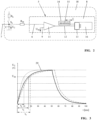
- the charging of the measuring capacitor C is shown schematically as an example for different charging curves 20 .
- the measurement voltage U M is below a maximum charging voltage of the capacitor C; for detecting the cell voltage U i of an individual cell Z i it is sufficient to consider a sub-branch of the charging curve 20 of the measuring capacitor C.
- the charging time t i which is required to charge the measuring capacitor C to the measuring voltage U M , can be determined via the counter reading of the counter 13 .
- the evaluation device 5 z. B. based on the charging time t 1 determined by the counter 13, the cell voltage Ui of the measured individual cell Z 1 .
- one counting unit of the counter 13 corresponds to a predetermined fixed time unit, namely a period T of the pulses 15. If a pulse sequence with a high frequency is selected, the counter 13 counts a large number of pulses 15 , whereby high resolution and high accuracy can be achieved with a simple structure. Counter readings of several thousand, tens of thousands or hundreds of thousands of units can be reached, depending on the selected frequency and pulse sequence. With little effort, a high degree of accuracy can be achieved, which is hardly possible with an A/D converter with justifiable effort.
- the evaluation device 5 for converting the count of the counter 13 into the cell voltage U i of the measured individual cell Z i is embodied in a microprocessor 8 .
- the counter 13 forms an integrated component of the microprocessor 8.
- the comparator 11 also forms an integrated component of the microprocessor 8.
Landscapes
- Physics & Mathematics (AREA)
- General Physics & Mathematics (AREA)
- Engineering & Computer Science (AREA)
- Power Engineering (AREA)
- Charge And Discharge Circuits For Batteries Or The Like (AREA)
- Measurement Of Current Or Voltage (AREA)
- Secondary Cells (AREA)
- Tests Of Electric Status Of Batteries (AREA)
Description
- Die Erfindung betrifft eine Schaltungsanordnung zur Bestimmung der Zellspannung einer Einzelzelle in einem Zellverbund eines Akkupacks nach dem Oberbegriff des Anspruchs 1.
- Aus der
DE 10 2007 049 528 B4 ist eine Schaltungsanordnung zur Messung der Zellspannungen von Einzelzellen eines Akkupacks bekannt. Die Einzelzellen bilden einen Zellverbund aus einer Reihenschaltung von Einzelzellen, wobei zwischen elektrisch benachbarten Einzelzellen der Reihenschaltung Potenzialpunkte ausgebildet sind. Die Potenziale der in der Reihenschaltung aufeinander folgenden Potenzialpunkte wachsen ausgehend von einem Bezugspotenzial im Betrag an. Jeder Potenzialpunkt der Reihenschaltung ist über einen Messwiderstand und einen Schalter mit einem Messeingang einer Auswertevorrichtung verbunden. Am Messwiderstand fällt nach Schließen des Schalters eine Spannung ab, die von der Auswertevorrichtung erfasst wird. Die einem Potenzialpunkt zugeordneten Messwiderstände sind nach Art einer Widerstandskaskade in Reihe geschaltet und bilden eine ohmsche Last der zu messenden Einzelzellen. Dabei bilden bei einer Messung der ersten Einzelzelle der Reihenschaltung der geschlossene Schalter und der erste Messwiderstand mit der ersten Einzelzelle einen ersten elektrischen Messkreis. Wird der zweite Schalter geschlossen - alle anderen Schalter sind offen -, bilden die erste Einzelzelle, die zweite Einzelzelle, der erste Messwiderstand und der zweite Messwiderstand einen geschlossenen Messkreis. Mit jeder Messung wird eine Einzelzelle elektrisch belastet, wobei die Belastung der ersten Einzelzellen einer Reihenschaltung größer ist als die der letzten Einzelzellen der Reihenschaltung. Die Einzelzellen werden jeweils durch Schließen der einzelnen Schalter gemessen, wobei jeweils die am Messwiderstand abfallende Spannung erfasst und ausgewertet wird. - Die
US 2004/0051534 A1 , dieEP 2 122 380 A2 und dieJP 2002 286 766 A1 - Der Aufwand einer derartigen Schaltungsanordnung zur Einzelspannungsmessung ist hoch; da die gemessenen Spannungen unter ohmscher Last erfasst werden, sind die Einzelzellen elektrisch stark belastet, wodurch die Standzeit des Akkupacks beeinflusst sein kann.
- Der Erfindung liegt die Aufgabe zugrunde, eine Schaltungsanordnung zur Bestimmung der Zellspannung einer Einzelzelle in einem Zellverbund aus einer Reihenschaltung von Einzelzellen eines Akkupacks anzugeben, welche einfach aufgebaut ist und eine geringe elektrische Belastung der Einzelzellen während der Messung aufweist.
- Die Aufgabe wird nach den Merkmalen des Anspruchs 1 gelöst.
- Der Messeingang der Auswertevorrichtung ist über einen Kondensator mit dem Bezugspotenzial verbunden, wobei die Auswertevorrichtung die Ladezeit des Kondensators auf eine vorgegebene Messspannung erfasst. Die Auswertevorrichtung bestimmt anhand der Ladezeit des Messkondensators die Zellspannung der gemessenen Einzelzelle.
- Vorteilhaft wird die Ladezeit des Messkondensators auf die Messspannung in einfacher Weise mittels eines Zählers erfasst, der mit dem Beginn der Messung anläuft und bei Erreichen der vorgegebenen Messspannung stoppt. Durch den Zähler wird in einfacher Weise unmittelbar die Ladezeit des Messkondensators in Zähleinheiten erfasst, wobei die Menge der Zähleinheiten vorzugsweise groß gewählt ist. So kann z. B. das Erreichen der Messspannung mit einem Zählerstand von mehreren Tausend oder Zehntausend gezählten Einheiten ausgelegt werden, was ohne großen technischen Aufwand eine hohe Auflösung ermöglicht. Gegenüber bekannten A/D Wandlern kann so eine hohe Genauigkeit erzielt werden.
- Der Zählerstand des Zählers ist der Ladezeit des Messkondensators auf die Messspannung proportional. Dabei kann die Zähleinheit des Zählers einer vorgegebenen festen Zeiteinheit entsprechen. In einfacher Weise zählt der Zähler die Impulse eines Zeitgliedes.
- Die Kondensatorspannung des Messkondensators wird auf einen ersten Eingang eines Komparators geschaltet, auf dessen zweiten Eingang ein Referenzwert entsprechend der vorgegebenen Messspannung aufgeschaltet ist. Der Ausgang des Komparators kann in einfacher Weise als Steuerungssignal auf den Zähler geschaltet sein. Der Ausgang des Komparators startet und stoppt den Zähler.
- Die Auswertevorrichtung zur Umrechnung des Zählerstandes in die Zellspannung der gemessenen Einzelzelle ist vorteilhaft in einem Mikroprozessor ausgebildet. In diesem Mikroprozessor kann auch der Zähler als integriertes Bauteil ausgeführt sein. Der Komparator ist zweckmäßig ein integriertes Bauteil des Mikroprozessors. Das Zeitglied wird von der "Clock" des Mikroprozessors gebildet, dessen Impulsfolge von dem Zähler gezählt wird.
- Vorteilhaft ist die vorgegebene Messspannung kleiner, insbesondere etwa 10% bis 95% kleiner als die Zellspannung einer vollständig geladenen Einzelzelle, so dass die elektrische Belastung der Einzelzelle während des Messvorgangs gering ist. Liegt die Zellspannung einer Einzelzelle im geladenen Zustand bei etwa 4,2 Volt, so kann die vorgegebene Messspannung z. B. bei nur 2000 mV liegen. Vorteilhaft liegt die vorgegebene Messspannung, die auch als Referenzwert zum Vergleich herangezogen wird, bei 1000 mV.
- Weitere Merkmale der Erfindung ergeben sich aus den weiteren Ansprüchen, der Beschreibung und der Zeichnung, in der ein Ausführungsbeispiel der Erfindung dargestellt ist. Es zeigen:
- Fig. 1
- in schematischer Darstellung eine Schaltungsanordnung zur Bestimmung der Zellspannung einer Einzelzelle in einem Zellverbund,
- Fig. 2
- in schematischer Darstellung ein Blockschaltbild einer Auswertevorrichtung,
- Fig. 3
- in schematischer Darstellung den Spannungsverlauf der Kondensatorspannung des Messkondensators.
- In
Fig. 1 ist ein Ausführungsbeispiel einer Schaltungsanordnung 10 von Einzelzellen Z1, Z2, Z3, Z4, Z5, Z6, Z7, Z8, Z9 bis Zn innerhalb eines Akkupacks 1 schematisch wiedergegeben. Die Einzelzellen Z1 bis Zn sind in einer Reihenschaltung 2 hintereinander geschaltet und stellen als Summenspannung gemeinsam eine Akkupackspannung UA zur Verfügung. Die Akkupackspannung UA setzt sich zusammen aus den Einzelspannungen U1, U2, U3, U4, U5, U6, U7, U8, U9 bis Un. Die Einzelzellen Z1 bis Zn bilden einen Zellverbund des Akkupacks. - Die Reihenschaltung 2 weist nach jeder Einzelzelle Z1 bis Zn einen Potenzialpunkt P1, P2, P3, P4, P5, P6, P7, P8, P9 bis Pn auf, wobei - wie an den Spannungspfeilen U1 bis Un zu ersehen - die Potenziale der in der Reihenschaltung 2 aufeinander folgenden Potenzialpunkte P1 bis Pn ausgehend von einem Bezugspotenzial 3 anwachsen. Das Bezugspotenzial 3 ist vorzugsweise das Massepotenzial.
- Jeder Potenzialpunkt P1 bis Pn ist über einen Messwiderstand R1, R2, R3, R4, R5, R6, R7, R8, R9 bis Rn und einen Schalter S1, S2, S3, S4, S5, S6, S7, S8, S9 bis Sn mit einem Messeingang 7 einer Auswertevorrichtung 5 verbunden.
- Im Folgenden wird das Bezugszeichen Zi, Pi, Ui, Si, Ri mit dem Index i allgemein für die Bezugszeichen Z1, Z2, ... Zn, P1, P2, ... Pn, U1, U2, ... Un, S1, S2, ... Sn, R1, R2, ... Rn, verwendet, wobei i für eine natürliche Zahl von 1 bis n steht. Beispielsweise ist so Zi als (Zi) mit i = 1, 2, 3, ...., n definiert.
- Aufgrund der dargestellten Schaltungsanordnung 10 liegen mit Schließen z. B. des Schalters S7 die Einzelspannungen U1, U2, U3, U4, U5, U6 und U7 der Teilreihenschaltung der Einzelzellen Z1, Z2, Z3, Z4, Z5, Z6 und Z7 als Summenspannung am Kondensator C an. Um unabhängig von dem gewählten Schalter Si am Kondensator C vergleichbare Messergebnisse abgreifen zu können, sind die Messwiderstände R1, R2, R3, R4, R5, R6, R7, R8, R9 bis Rn in ihrer Größe angepasst gewählt. So wird für den ersten Widerstand R1 z. B. ein Wert von 10kΩ gewählt; die folgenden Messwiderstände R2, R3, R4, R5, R6, R7, R8, R9 bis Rn sind mit wachsenden Werten ausgebildet; bei zehn Messwiderständen Rn hat der letzte Messwiderstand Rn einen Wert von z. B. 100kΩ. Auf diese Weise werden die elektrischen Bedingungen zur Messung einer Einzelspannung Ui an einer Einzelzelle Zi abhängig von dem geschlossenen Schalter Si angepasst. Jeder aktive Messzweig ist so mit τ = R•C statisch kalibriert worden.
- Der Messeingang 7 der Auswertevorrichtung 5 ist über einen Kondensator C mit dem Bezugspotenzial 3 verbunden. Über einen Schalter SK und einen Ohm'schen Widerstand RK ist der positive Anschluss des Kondensators C mit einer Kalibrierspannung 4 verbunden.
- Es kann zweckmäßig sein, die Auswertevorrichtung 5 mit einem zweiten Messeingang und einem zweiten Messkondensator zu versehen, wodurch die Gesamtdauer der Messung aller z. B. zehn Einzelzellen verringert werden kann. So können auch bei größeren Akkumulatoren mit Anordnungen von einer größeren Anzahl von Einzelzellen ausreichend Messanordnungen zur Verfügung gestellt werden, die eine sichere elektrische Überwachung gewährleisten.
- Jeder Messeingang wird zusammen mit dem zugeordneten Messkondensator C einzeln kalibriert, und die Werte der Kalibrierung werden vorteilhaft in einem Mikroprozessor 8 abgelegt. Vorteilhaft erfolgt eine dynamische Kalibrierung derart, dass nach jeder Messung ein Kalibrierprozess durchlaufen wird, so dass eine Alterung oder ein Temperaturdrift des Messkondensators C ausgeglichen wird.
- Die zwischen dem Bezugspotenzial 3 und dem Messeingang 7 abzugreifende Kondensatorspannung Uc wird über einen Eingangswiderstand RM einem Mikroprozessor 8 zugeführt.
- Die Kondensatorspannung Uc wird auf einen ersten Eingang 6 eines Komparators 11 geschaltet. An dem anderen, zweiten Eingang 9 des Komparators liegt ein Referenzwert in Form einer vorgegebenen Messspannung UM an.
- Der Ausgang 12 des Komparators steuert einen Zähler 13, der die Impulse 15 eines Zeitgliedes 14 zählt. In einer Berechnungseinheit 16, der unmittelbar der Zählerstand des Zählers 13 übermittelt wird, wird anhand der gezählten Impulse 15 die Ladezeit t des Kondensators C auf die als Referenzwert vorgegebene Messspannung UM ermittelt. Der Mikroprozessor 8 kann anhand der Ladezeit ti auf die Zellspannung Ui der gemessenen Einzelzelle Zi schließen.
- Wird z. B. die Zelle Z1 durch Schließen des Schalters S1 an den Messkondensator C angelegt, so wird mit Schließen des Schalters S1 der Zähler 13 gestartet. Am Komparator 11 liegt einerseits die Kondensatorspannung Uc an; am anderen Eingang 9 des Komparators liegt die Messspannung UM als Referenzwert an. Während des Aufladens des Kondensators C zählt der Zähler 13 die Impulse 15 des Zeitgliedes 14. Sobald die Kondensatorspannung Uc den Referenzwert der Messspannung UM erreicht, wird über den Ausgang 12 des Komparators 11 der Zähler 13 gestoppt. Der Zählerstand ist proportional einer Zeit - hier der Ladezeit t1 -, da der Zählerstand einer Anzahl von Impulsen 15 des Zeitgliedes 14 entspricht. Es ist eine normierte Ladung des Kondensators umgesetzt.
- In
Fig. 3 ist schematisch die Aufladung des Messkondensators C beispielhaft für verschiedene Ladekurven 20 wiedergegeben. Wie dargestellt, liegt die Messspannung UM unterhalb einer maximalen Ladespannung des Kondensators C; für die Erfassung der Zellspannung Ui einer Einzelzelle Zi ist ausreichend, einen Teilzweig der Ladekurve 20 des Messkondensators C zu betrachten. Über den Zählerstand des Zählers 13 kann die Ladezeit ti bestimmt werden, die benötigt wird, um den Messkondensator C auf die Messspannung UM aufzuladen. So bestimmt die Auswertevorrichtung 5 z. B. anhand der über den Zähler 13 ermittelten Ladezeit t1 die Zellspannung Ui der gemessenen Einzelzelle Z1. - Da das Zeitglied 14 eine zeitstabile Impulsfolge aus Impulsen 15 bereitstellt, entspricht eine Zähleinheit des Zählers 13 einer vorgegebenen festen Zeiteinheit, nämlich einer Periode T der Impulse 15. Wird eine Impulsfolge mit hoher Frequenz gewählt, wird vom Zähler 13 eine große Anzahl von Impulsen 15 gezählt, wodurch bei einfachem Aufbau eine hohe Auflösung und eine hohe Genauigkeit zu erzielen sind. Es können Zählerstände von mehreren Tausend, Zehntausend oder Hunderttausend Einheiten erreicht werden, je nach gewählter Frequenz und Impulsfolge. Bei geringem Aufwand ist so eine hohe Genauigkeit erreichbar, die in dieser Güte mit einem A/D-Wandler mit vertretbarem Aufwand kaum möglich ist.
- Die Auswertevorrichtung 5 zur Umrechnung des Zählerstandes des Zählers 13 in die Zellspannung Ui der gemessenen Einzelzelle Zi ist in einem Mikroprozessor 8 ausgebildet. Dabei bildet der Zähler 13 ein integriertes Bauteil des Mikroprozessors 8. In gleicher Weise bildet auch der Komparator 11 ein integriertes Bauteil des Mikroprozessors 8.
Claims (13)
- Schaltungsanordnung mit einer Auswertevorrichtung (5) zur Bestimmung der Zellspannung (Ui) einer Einzelzelle (Zi) in einem Zellverbund aus einer Reihenschaltung (2) von Einzelzellen (Zi) eines Akkupacks (1),wobei zwischen elektrisch benachbarten Einzelzellen (Zi) der Reihenschaltung (2) jeweils ein Potenzialpunkt (Pi) ausgebildet ist, und die Potenziale der in der Reihenschaltung (2) aufeinander folgenden Potenzialpunkte (Pi) ausgehend von einem Bezugspotenzial (3) im Betrag anwachsen,wobei jeder Potenzialpunkt (Pi) der Reihenschaltung (2) über einen Messwiderstand (Ri) und einen Schalter (Si) mit einem Messeingang (7) der Auswertevorrichtung (5) verbunden ist,wobei durch die Schaltungsanordnung (10) ein erster Potenzialpunkt (P1) mit einem ersten Widerstand (R1) mit dem Messeingang (7) verbunden ist, und die in der Reihe folgenden Potenzialpunkte (Pi) der Schaltungsanordnung (10) über Messwiderstände (Ri) mit anwachsenden Werten mit dem Messeingang (7) verbunden sind, unddie Schaltungsanordnung (10) ausgebildet ist, durch Schließen eines Schalters (Si) die Einzelspannungen (Ui) einer Teilreihenschaltung der Einzelzellen (Zi) als Summenspannung auf den Messeingang (7) zu schalten,dadurch gekennzeichnet,- dass der Messeingang (7) über einen Messkondensator (C) mit dem Bezugspotenzial (3) verbunden ist, und die Auswertevorrichtung (5) ausgebildet ist, die Ladezeit (ti) des Messkondensators (C) auf eine vorgegebene Messspannung (UM) zu erfassen,- und dass die Auswertevorrichtung (5) ausgebildet ist, anhand der Ladezeit (ti) des Messkondensators (C) und der Zeitkonstante des jeweiligen aktiven Messzweigs (Ri ∗C) das Potenzial des Potenzialpunktes und die Zellspannung (Ui) der Einzelzelle (Zi) zu bestimmen.
- Schaltungsanordnung nach Anspruch 1,
weiter ausgebildet, die Ladezeit (ti) des Messkondensators (C) auf die Messspannung (UM) mittels eines Zählers (13) zu erfassen, der mit dem Beginn der Messung anläuft und bei Erreichen der vorgegebenen Messspannung (UM) stoppt. - Schaltungsanordnung nach Anspruch 2,
dadurch gekennzeichnet, dass der Zählerstand des Zählers (13) der Ladezeit (ti) des Messkondensators (C) auf die Messspannung (UM) proportional ist. - Schaltungsanordnung nach Anspruch 3,
dadurch gekennzeichnet, dass eine Zähleinheit des Zählers (13) einer vorgegebenen Zeiteinheit (ti) entspricht. - Schaltungsanordnung nach Anspruch 4,
dadurch gekennzeichnet, dass der Zähler (13) die Impulse (15) eines Zeitgliedes (14) zählt. - Schaltungsanordnung nach Anspruch 2,
weiter ausgebildet, die Kondensatorspannung (Uc) des Messkondensators (C) auf einen ersten Eingang (6) eines Komparators (11) zu schalten, und auf einen zweiten Eingang (9) des Komparators ein Referenzwert entsprechend der vorgegebenen Messspannung (UM) aufzuschalten. - Schaltungsanordnung nach Anspruch 6, weiter ausgebildet, den Ausgang (12) des Komparators (11) als Steuerungssignal auf den Zähler (13) zu schalten.
- Schaltungsanordnung nach einem der Ansprüche 1 bis 7,
dadurch gekennzeichnet, dass die Auswertevorrichtung (5) zur Umrechnung des Zählerstandes in die Zellspannung (Ui) der gemessenen Einzelzelle (Zi) in einem Mikroprozessor (8) ausgebildet ist. - Schaltungsanordnung nach Anspruch 8,
dadurch gekennzeichnet, dass der Zähler (13) ein integriertes Bauteil des Mikroprozessors (8) ist. - Schaltungsanordnung nach Anspruch 7,
dadurch gekennzeichnet, dass ein Komparator zum Vergleich der Kondensatorspannung (Uc) des Messkondensators (C) mit einem Referenzwert als integriertes Bauteil des Mikroprozessors (8) ausgebildet ist. - Schaltungsanordnung nach Anspruch 9,
dadurch gekennzeichnet, dass der Zähler (13) den Takt eines internen Taktgebers des Mikroprozessors (8) zählt. - Schaltungsanordnung nach einem der Ansprüche 1 bis 11,
dadurch gekennzeichnet, dass die Messspannung (UM) kleiner ist als die Zellspannung (Ui) einer Einzelzelle (Zi). - Schaltungsanordnung nach Anspruch 1,
dadurch gekennzeichnet, dass die Messwiderstände (Ri) in ihrer Größe derart gewählt sind, dass unabhängig von dem gewählten Schalter (Si) am Kondensator (C) vergleichbare Messergebnisse abgegriffen werden.
Applications Claiming Priority (1)
| Application Number | Priority Date | Filing Date | Title |
|---|---|---|---|
| DE102016001057.6A DE102016001057A1 (de) | 2016-01-30 | 2016-01-30 | Schaltungsanordnung zur Bestimmung der Zellspannung einer Einzelzelle in einem Zellverbund |
Publications (2)
| Publication Number | Publication Date |
|---|---|
| EP3203252A1 EP3203252A1 (de) | 2017-08-09 |
| EP3203252B1 true EP3203252B1 (de) | 2023-06-21 |
Family
ID=57890647
Family Applications (1)
| Application Number | Title | Priority Date | Filing Date |
|---|---|---|---|
| EP17000108.5A Active EP3203252B1 (de) | 2016-01-30 | 2017-01-23 | Schaltungsanordnung zur bestimmung der zellspannung einer einzelzelle in einem zellverbund |
Country Status (4)
| Country | Link |
|---|---|
| US (1) | US10401437B2 (de) |
| EP (1) | EP3203252B1 (de) |
| CN (1) | CN107024660B (de) |
| DE (1) | DE102016001057A1 (de) |
Families Citing this family (2)
| Publication number | Priority date | Publication date | Assignee | Title |
|---|---|---|---|---|
| DE102019200510A1 (de) * | 2019-01-16 | 2020-07-16 | Audi Ag | Messanordnung, Hochvoltbatterie, Kraftfahrzeug und Verfahren zum Bestimmen einer komplexen Impedanz |
| EP4166962B1 (de) * | 2021-10-15 | 2024-06-19 | Andreas Stihl AG & Co. KG | Elektrischer energiespeicher |
Family Cites Families (8)
| Publication number | Priority date | Publication date | Assignee | Title |
|---|---|---|---|---|
| JP4540029B2 (ja) * | 2001-03-23 | 2010-09-08 | 株式会社Gsユアサ | 電圧検出方法及び電圧検出装置 |
| JP3791767B2 (ja) * | 2001-03-27 | 2006-06-28 | 株式会社デンソー | フライングキャパシタ式電圧検出回路 |
| DE10207062A1 (de) * | 2002-02-20 | 2003-08-28 | Philips Intellectual Property | Verfahren und Schaltungsanordnung zur Ermittlung des mittleren Stromverbrauchs eines batteriebetriebenen Gerätes |
| US7772803B2 (en) * | 2007-01-07 | 2010-08-10 | Enerdel, Inc. | Method and system to measure series-connected cell voltages using a flying capacitor |
| DE102007049528B4 (de) | 2007-10-15 | 2009-06-25 | Panasonic Electronic Devices Europe Gmbh | Verfahren und Vorrichtung zur Messung von Zellenspannungen in einer Mehrzahl von in Reihe geschalteten Akkumulatorzellen |
| WO2010062141A2 (ko) * | 2008-11-27 | 2010-06-03 | 주식회사 엘지화학 | 배터리 셀 전압 측정 장치 및 방법 |
| DE102014204959A1 (de) * | 2014-03-18 | 2015-09-24 | Robert Bosch Gmbh | Batteriezelleinrichtung mit einer Batteriezelle und einer Temperaturmessschaltung zum Bestimmen der Temperatur der Batteriezelle und entsprechendes Verfahren |
| FR3039006B1 (fr) * | 2015-07-17 | 2019-05-03 | Commissariat A L'energie Atomique Et Aux Energies Alternatives | Dispositif de gestion d'un assemblage de cellules de stockage ou de production d'energie electrique |
-
2016
- 2016-01-30 DE DE102016001057.6A patent/DE102016001057A1/de active Pending
-
2017
- 2017-01-23 EP EP17000108.5A patent/EP3203252B1/de active Active
- 2017-01-26 CN CN201710057074.2A patent/CN107024660B/zh active Active
- 2017-01-30 US US15/419,752 patent/US10401437B2/en active Active
Also Published As
| Publication number | Publication date |
|---|---|
| DE102016001057A1 (de) | 2017-08-03 |
| CN107024660A (zh) | 2017-08-08 |
| EP3203252A1 (de) | 2017-08-09 |
| US10401437B2 (en) | 2019-09-03 |
| US20170219658A1 (en) | 2017-08-03 |
| CN107024660B (zh) | 2021-12-07 |
Similar Documents
| Publication | Publication Date | Title |
|---|---|---|
| EP3701274B1 (de) | Verfahren zum betrieb eines batteriesensors und batteriesensor | |
| EP2442125B1 (de) | Verfahren und Vorrichtung zum Überwachen der maximal verfügbaren Kapazität einer Batterie | |
| EP0188477A1 (de) | Verfahren und einrichtung zur überwachung des ladezustandes von wiederaufladbaren batterien. | |
| DE102012206893A1 (de) | Verfahren und Vorrichtung zum Bestimmen eines Ladezustands einer Batterie und Batterie | |
| WO2013178330A1 (de) | Verfahren und vorrichtung zum feststellen der tatsächlichen kapazität einer batterie | |
| EP3449264B1 (de) | Verfahren zum bestimmen eines laststroms und batteriesensor | |
| DE102016201026B4 (de) | Verfahren und Vorrichtung zur Bestimmung einer Restkapazität einer Blei-Säure-Batterie | |
| DE102020125127A1 (de) | Verfahren zur Bestimmung des Zustands eines wiederaufladbaren Batteriesystems | |
| EP3203252B1 (de) | Schaltungsanordnung zur bestimmung der zellspannung einer einzelzelle in einem zellverbund | |
| EP0154033A1 (de) | Prüfverfahren für Gleichstromquellen wie Akkumulatoren, Batterien oder dgl. und Prüfgerät | |
| DE102014220913A1 (de) | Verfahren und Vorrichtung zur Bestimmung einer Widerstandsänderung einer Energiespeichereinrichtung und Fahrzeug | |
| DE102014007304A1 (de) | Kraftfahrzeug-Batteriemanagement mit Einzelzellenüberwachung | |
| DE102014219807B4 (de) | Verfahren und Vorrichtung zur Prüfung einer Funktionsfähigkeit eines Stromsensors und Fahrzeug | |
| EP0836085B1 (de) | Widerstandsmessschaltung und Widerstandsmessverfahren | |
| EP3362810B1 (de) | Fortbewegungsmittel, vorrichtung und verfahren zur ermittlung einer spannung einer zelle eines strangs mehrerer in reihe geschalteter zellen eines elektrochemischen energiespeichers | |
| DE102014219806A1 (de) | Verfahren und Vorrichtung zur Prüfung einer Funktionsfähigkeit eines Stromsensors und Fahrzeug | |
| DE102019132768A1 (de) | Kalibriereinrichtung zur Kalibrierung einer elekrischen Ersatzschaltung | |
| DE3031452A1 (de) | Schaltungsanordnung zum messen von spitzenwerten eines nicht periodischen vorganges mit geringer wiederholungsfolge | |
| DE3213516C1 (en) | Method and arrangement for determining the state of aging of a secondary battery | |
| EP4616212A1 (de) | Verfahren und vorrichtung zur bestimmung von kapazität, innenwiderstand und leerlaufspannungskurve einer batterie | |
| DE102016006419A1 (de) | Gleichstromimpuls-Batterietestgerät und Verfahren zur Erkennung eines Batterietyps | |
| DE102019126136A1 (de) | Verfahren und Einrichtung zum Ermitteln einer eine Temperatur eines Widerstandstemperaturfühlers beschreibenden Temperaturinformation, Wechselrichter, Fahrzeug und Computerprogramm | |
| DE102005029890A1 (de) | Zustandserkennung für mehrere in Serie geschaltete Batteriezellen | |
| DE102010046605A1 (de) | Batteriesteuergerät mit einem Modell zur Ermittlung der Batterielebensdauer | |
| DE102015219823A1 (de) | Elektrisch antreibbares Fortbewegungsmittel, Vorrichtung und Verfahren zur Ermittlung einer Spannung einer Zelle eines Strangs mehrerer in Reihe geschalteter Zellen eines elektrochemischen Energiespeichers |
Legal Events
| Date | Code | Title | Description |
|---|---|---|---|
| PUAI | Public reference made under article 153(3) epc to a published international application that has entered the european phase |
Free format text: ORIGINAL CODE: 0009012 |
|
| STAA | Information on the status of an ep patent application or granted ep patent |
Free format text: STATUS: THE APPLICATION HAS BEEN PUBLISHED |
|
| AK | Designated contracting states |
Kind code of ref document: A1 Designated state(s): AL AT BE BG CH CY CZ DE DK EE ES FI FR GB GR HR HU IE IS IT LI LT LU LV MC MK MT NL NO PL PT RO RS SE SI SK SM TR |
|
| AX | Request for extension of the european patent |
Extension state: BA ME |
|
| STAA | Information on the status of an ep patent application or granted ep patent |
Free format text: STATUS: REQUEST FOR EXAMINATION WAS MADE |
|
| 17P | Request for examination filed |
Effective date: 20180205 |
|
| RBV | Designated contracting states (corrected) |
Designated state(s): AL AT BE BG CH CY CZ DE DK EE ES FI FR GB GR HR HU IE IS IT LI LT LU LV MC MK MT NL NO PL PT RO RS SE SI SK SM TR |
|
| STAA | Information on the status of an ep patent application or granted ep patent |
Free format text: STATUS: EXAMINATION IS IN PROGRESS |
|
| 17Q | First examination report despatched |
Effective date: 20200609 |
|
| GRAP | Despatch of communication of intention to grant a patent |
Free format text: ORIGINAL CODE: EPIDOSNIGR1 |
|
| STAA | Information on the status of an ep patent application or granted ep patent |
Free format text: STATUS: GRANT OF PATENT IS INTENDED |
|
| INTG | Intention to grant announced |
Effective date: 20230117 |
|
| RIN1 | Information on inventor provided before grant (corrected) |
Inventor name: KULZER, MARKUS Inventor name: HEIGEMEYR, CHRISTIAN Inventor name: LIEBHARD, GERNOT Inventor name: SCHURR, MARTIN |
|
| GRAS | Grant fee paid |
Free format text: ORIGINAL CODE: EPIDOSNIGR3 |
|
| GRAA | (expected) grant |
Free format text: ORIGINAL CODE: 0009210 |
|
| STAA | Information on the status of an ep patent application or granted ep patent |
Free format text: STATUS: THE PATENT HAS BEEN GRANTED |
|
| AK | Designated contracting states |
Kind code of ref document: B1 Designated state(s): AL AT BE BG CH CY CZ DE DK EE ES FI FR GB GR HR HU IE IS IT LI LT LU LV MC MK MT NL NO PL PT RO RS SE SI SK SM TR |
|
| REG | Reference to a national code |
Ref country code: CH Ref legal event code: EP |
|
| REG | Reference to a national code |
Ref country code: DE Ref legal event code: R096 Ref document number: 502017014932 Country of ref document: DE |
|
| REG | Reference to a national code |
Ref country code: AT Ref legal event code: REF Ref document number: 1581258 Country of ref document: AT Kind code of ref document: T Effective date: 20230715 |
|
| REG | Reference to a national code |
Ref country code: IE Ref legal event code: FG4D Free format text: LANGUAGE OF EP DOCUMENT: GERMAN |
|
| REG | Reference to a national code |
Ref country code: LT Ref legal event code: MG9D |
|
| REG | Reference to a national code |
Ref country code: NL Ref legal event code: MP Effective date: 20230621 |
|
| PG25 | Lapsed in a contracting state [announced via postgrant information from national office to epo] |
Ref country code: SE Free format text: LAPSE BECAUSE OF FAILURE TO SUBMIT A TRANSLATION OF THE DESCRIPTION OR TO PAY THE FEE WITHIN THE PRESCRIBED TIME-LIMIT Effective date: 20230621 Ref country code: NO Free format text: LAPSE BECAUSE OF FAILURE TO SUBMIT A TRANSLATION OF THE DESCRIPTION OR TO PAY THE FEE WITHIN THE PRESCRIBED TIME-LIMIT Effective date: 20230921 |
|
| PG25 | Lapsed in a contracting state [announced via postgrant information from national office to epo] |
Ref country code: RS Free format text: LAPSE BECAUSE OF FAILURE TO SUBMIT A TRANSLATION OF THE DESCRIPTION OR TO PAY THE FEE WITHIN THE PRESCRIBED TIME-LIMIT Effective date: 20230621 Ref country code: NL Free format text: LAPSE BECAUSE OF FAILURE TO SUBMIT A TRANSLATION OF THE DESCRIPTION OR TO PAY THE FEE WITHIN THE PRESCRIBED TIME-LIMIT Effective date: 20230621 Ref country code: LV Free format text: LAPSE BECAUSE OF FAILURE TO SUBMIT A TRANSLATION OF THE DESCRIPTION OR TO PAY THE FEE WITHIN THE PRESCRIBED TIME-LIMIT Effective date: 20230621 Ref country code: LT Free format text: LAPSE BECAUSE OF FAILURE TO SUBMIT A TRANSLATION OF THE DESCRIPTION OR TO PAY THE FEE WITHIN THE PRESCRIBED TIME-LIMIT Effective date: 20230621 Ref country code: HR Free format text: LAPSE BECAUSE OF FAILURE TO SUBMIT A TRANSLATION OF THE DESCRIPTION OR TO PAY THE FEE WITHIN THE PRESCRIBED TIME-LIMIT Effective date: 20230621 Ref country code: GR Free format text: LAPSE BECAUSE OF FAILURE TO SUBMIT A TRANSLATION OF THE DESCRIPTION OR TO PAY THE FEE WITHIN THE PRESCRIBED TIME-LIMIT Effective date: 20230922 |
|
| PG25 | Lapsed in a contracting state [announced via postgrant information from national office to epo] |
Ref country code: FI Free format text: LAPSE BECAUSE OF FAILURE TO SUBMIT A TRANSLATION OF THE DESCRIPTION OR TO PAY THE FEE WITHIN THE PRESCRIBED TIME-LIMIT Effective date: 20230621 |
|
| PG25 | Lapsed in a contracting state [announced via postgrant information from national office to epo] |
Ref country code: SK Free format text: LAPSE BECAUSE OF FAILURE TO SUBMIT A TRANSLATION OF THE DESCRIPTION OR TO PAY THE FEE WITHIN THE PRESCRIBED TIME-LIMIT Effective date: 20230621 |
|
| PG25 | Lapsed in a contracting state [announced via postgrant information from national office to epo] |
Ref country code: ES Free format text: LAPSE BECAUSE OF FAILURE TO SUBMIT A TRANSLATION OF THE DESCRIPTION OR TO PAY THE FEE WITHIN THE PRESCRIBED TIME-LIMIT Effective date: 20230621 |
|
| PG25 | Lapsed in a contracting state [announced via postgrant information from national office to epo] |
Ref country code: IS Free format text: LAPSE BECAUSE OF FAILURE TO SUBMIT A TRANSLATION OF THE DESCRIPTION OR TO PAY THE FEE WITHIN THE PRESCRIBED TIME-LIMIT Effective date: 20231021 |
|
| PG25 | Lapsed in a contracting state [announced via postgrant information from national office to epo] |
Ref country code: SM Free format text: LAPSE BECAUSE OF FAILURE TO SUBMIT A TRANSLATION OF THE DESCRIPTION OR TO PAY THE FEE WITHIN THE PRESCRIBED TIME-LIMIT Effective date: 20230621 Ref country code: SK Free format text: LAPSE BECAUSE OF FAILURE TO SUBMIT A TRANSLATION OF THE DESCRIPTION OR TO PAY THE FEE WITHIN THE PRESCRIBED TIME-LIMIT Effective date: 20230621 Ref country code: RO Free format text: LAPSE BECAUSE OF FAILURE TO SUBMIT A TRANSLATION OF THE DESCRIPTION OR TO PAY THE FEE WITHIN THE PRESCRIBED TIME-LIMIT Effective date: 20230621 Ref country code: PT Free format text: LAPSE BECAUSE OF FAILURE TO SUBMIT A TRANSLATION OF THE DESCRIPTION OR TO PAY THE FEE WITHIN THE PRESCRIBED TIME-LIMIT Effective date: 20231023 Ref country code: IS Free format text: LAPSE BECAUSE OF FAILURE TO SUBMIT A TRANSLATION OF THE DESCRIPTION OR TO PAY THE FEE WITHIN THE PRESCRIBED TIME-LIMIT Effective date: 20231021 Ref country code: ES Free format text: LAPSE BECAUSE OF FAILURE TO SUBMIT A TRANSLATION OF THE DESCRIPTION OR TO PAY THE FEE WITHIN THE PRESCRIBED TIME-LIMIT Effective date: 20230621 Ref country code: EE Free format text: LAPSE BECAUSE OF FAILURE TO SUBMIT A TRANSLATION OF THE DESCRIPTION OR TO PAY THE FEE WITHIN THE PRESCRIBED TIME-LIMIT Effective date: 20230621 Ref country code: CZ Free format text: LAPSE BECAUSE OF FAILURE TO SUBMIT A TRANSLATION OF THE DESCRIPTION OR TO PAY THE FEE WITHIN THE PRESCRIBED TIME-LIMIT Effective date: 20230621 |
|
| PG25 | Lapsed in a contracting state [announced via postgrant information from national office to epo] |
Ref country code: PL Free format text: LAPSE BECAUSE OF FAILURE TO SUBMIT A TRANSLATION OF THE DESCRIPTION OR TO PAY THE FEE WITHIN THE PRESCRIBED TIME-LIMIT Effective date: 20230621 |
|
| REG | Reference to a national code |
Ref country code: DE Ref legal event code: R097 Ref document number: 502017014932 Country of ref document: DE |
|
| PLBE | No opposition filed within time limit |
Free format text: ORIGINAL CODE: 0009261 |
|
| STAA | Information on the status of an ep patent application or granted ep patent |
Free format text: STATUS: NO OPPOSITION FILED WITHIN TIME LIMIT |
|
| PG25 | Lapsed in a contracting state [announced via postgrant information from national office to epo] |
Ref country code: DK Free format text: LAPSE BECAUSE OF FAILURE TO SUBMIT A TRANSLATION OF THE DESCRIPTION OR TO PAY THE FEE WITHIN THE PRESCRIBED TIME-LIMIT Effective date: 20230621 |
|
| PG25 | Lapsed in a contracting state [announced via postgrant information from national office to epo] |
Ref country code: SI Free format text: LAPSE BECAUSE OF FAILURE TO SUBMIT A TRANSLATION OF THE DESCRIPTION OR TO PAY THE FEE WITHIN THE PRESCRIBED TIME-LIMIT Effective date: 20230621 |
|
| 26N | No opposition filed |
Effective date: 20240322 |
|
| PG25 | Lapsed in a contracting state [announced via postgrant information from national office to epo] |
Ref country code: SI Free format text: LAPSE BECAUSE OF FAILURE TO SUBMIT A TRANSLATION OF THE DESCRIPTION OR TO PAY THE FEE WITHIN THE PRESCRIBED TIME-LIMIT Effective date: 20230621 Ref country code: IT Free format text: LAPSE BECAUSE OF FAILURE TO SUBMIT A TRANSLATION OF THE DESCRIPTION OR TO PAY THE FEE WITHIN THE PRESCRIBED TIME-LIMIT Effective date: 20230621 |
|
| PG25 | Lapsed in a contracting state [announced via postgrant information from national office to epo] |
Ref country code: MC Free format text: LAPSE BECAUSE OF FAILURE TO SUBMIT A TRANSLATION OF THE DESCRIPTION OR TO PAY THE FEE WITHIN THE PRESCRIBED TIME-LIMIT Effective date: 20230621 |
|
| PG25 | Lapsed in a contracting state [announced via postgrant information from national office to epo] |
Ref country code: MC Free format text: LAPSE BECAUSE OF FAILURE TO SUBMIT A TRANSLATION OF THE DESCRIPTION OR TO PAY THE FEE WITHIN THE PRESCRIBED TIME-LIMIT Effective date: 20230621 |
|
| REG | Reference to a national code |
Ref country code: CH Ref legal event code: PL |
|
| PG25 | Lapsed in a contracting state [announced via postgrant information from national office to epo] |
Ref country code: LU Free format text: LAPSE BECAUSE OF NON-PAYMENT OF DUE FEES Effective date: 20240123 |
|
| GBPC | Gb: european patent ceased through non-payment of renewal fee |
Effective date: 20240123 |
|
| PG25 | Lapsed in a contracting state [announced via postgrant information from national office to epo] |
Ref country code: LU Free format text: LAPSE BECAUSE OF NON-PAYMENT OF DUE FEES Effective date: 20240123 |
|
| PG25 | Lapsed in a contracting state [announced via postgrant information from national office to epo] |
Ref country code: GB Free format text: LAPSE BECAUSE OF NON-PAYMENT OF DUE FEES Effective date: 20240123 |
|
| PG25 | Lapsed in a contracting state [announced via postgrant information from national office to epo] |
Ref country code: BE Free format text: LAPSE BECAUSE OF NON-PAYMENT OF DUE FEES Effective date: 20240131 |
|
| PG25 | Lapsed in a contracting state [announced via postgrant information from national office to epo] |
Ref country code: CH Free format text: LAPSE BECAUSE OF NON-PAYMENT OF DUE FEES Effective date: 20240131 |
|
| PG25 | Lapsed in a contracting state [announced via postgrant information from national office to epo] |
Ref country code: GB Free format text: LAPSE BECAUSE OF NON-PAYMENT OF DUE FEES Effective date: 20240123 Ref country code: CH Free format text: LAPSE BECAUSE OF NON-PAYMENT OF DUE FEES Effective date: 20240131 Ref country code: BE Free format text: LAPSE BECAUSE OF NON-PAYMENT OF DUE FEES Effective date: 20240131 |
|
| REG | Reference to a national code |
Ref country code: BE Ref legal event code: MM Effective date: 20240131 |
|
| PG25 | Lapsed in a contracting state [announced via postgrant information from national office to epo] |
Ref country code: BG Free format text: LAPSE BECAUSE OF FAILURE TO SUBMIT A TRANSLATION OF THE DESCRIPTION OR TO PAY THE FEE WITHIN THE PRESCRIBED TIME-LIMIT Effective date: 20230621 |
|
| PG25 | Lapsed in a contracting state [announced via postgrant information from national office to epo] |
Ref country code: BG Free format text: LAPSE BECAUSE OF FAILURE TO SUBMIT A TRANSLATION OF THE DESCRIPTION OR TO PAY THE FEE WITHIN THE PRESCRIBED TIME-LIMIT Effective date: 20230621 |
|
| PG25 | Lapsed in a contracting state [announced via postgrant information from national office to epo] |
Ref country code: IE Free format text: LAPSE BECAUSE OF NON-PAYMENT OF DUE FEES Effective date: 20240123 |
|
| PG25 | Lapsed in a contracting state [announced via postgrant information from national office to epo] |
Ref country code: IE Free format text: LAPSE BECAUSE OF NON-PAYMENT OF DUE FEES Effective date: 20240123 |
|
| REG | Reference to a national code |
Ref country code: AT Ref legal event code: MM01 Ref document number: 1581258 Country of ref document: AT Kind code of ref document: T Effective date: 20240123 |
|
| PG25 | Lapsed in a contracting state [announced via postgrant information from national office to epo] |
Ref country code: AT Free format text: LAPSE BECAUSE OF NON-PAYMENT OF DUE FEES Effective date: 20240123 |
|
| PG25 | Lapsed in a contracting state [announced via postgrant information from national office to epo] |
Ref country code: CY Free format text: LAPSE BECAUSE OF FAILURE TO SUBMIT A TRANSLATION OF THE DESCRIPTION OR TO PAY THE FEE WITHIN THE PRESCRIBED TIME-LIMIT; INVALID AB INITIO Effective date: 20170123 |
|
| PG25 | Lapsed in a contracting state [announced via postgrant information from national office to epo] |
Ref country code: HU Free format text: LAPSE BECAUSE OF FAILURE TO SUBMIT A TRANSLATION OF THE DESCRIPTION OR TO PAY THE FEE WITHIN THE PRESCRIBED TIME-LIMIT; INVALID AB INITIO Effective date: 20170123 |
|
| PG25 | Lapsed in a contracting state [announced via postgrant information from national office to epo] |
Ref country code: TR Free format text: LAPSE BECAUSE OF FAILURE TO SUBMIT A TRANSLATION OF THE DESCRIPTION OR TO PAY THE FEE WITHIN THE PRESCRIBED TIME-LIMIT Effective date: 20230621 |
|
| PGFP | Annual fee paid to national office [announced via postgrant information from national office to epo] |
Ref country code: DE Payment date: 20260127 Year of fee payment: 10 |
|
| PGFP | Annual fee paid to national office [announced via postgrant information from national office to epo] |
Ref country code: FR Payment date: 20260126 Year of fee payment: 10 |