EP3203461A2 - Zeitkontrollierer - Google Patents
Zeitkontrollierer Download PDFInfo
- Publication number
- EP3203461A2 EP3203461A2 EP17153988.5A EP17153988A EP3203461A2 EP 3203461 A2 EP3203461 A2 EP 3203461A2 EP 17153988 A EP17153988 A EP 17153988A EP 3203461 A2 EP3203461 A2 EP 3203461A2
- Authority
- EP
- European Patent Office
- Prior art keywords
- data
- segment
- timing controller
- character
- sub
- Prior art date
- Legal status (The legal status is an assumption and is not a legal conclusion. Google has not performed a legal analysis and makes no representation as to the accuracy of the status listed.)
- Ceased
Links
- 238000012545 processing Methods 0.000 claims abstract description 38
- 238000010586 diagram Methods 0.000 description 35
- 238000012986 modification Methods 0.000 description 26
- 230000004048 modification Effects 0.000 description 26
- 238000013144 data compression Methods 0.000 description 9
- 239000011159 matrix material Substances 0.000 description 5
- 239000004065 semiconductor Substances 0.000 description 4
- 239000000758 substrate Substances 0.000 description 4
- 230000005540 biological transmission Effects 0.000 description 3
- 230000006870 function Effects 0.000 description 3
- 230000007257 malfunction Effects 0.000 description 3
- 238000000034 method Methods 0.000 description 3
- 101100422768 Saccharomyces cerevisiae (strain ATCC 204508 / S288c) SUL2 gene Proteins 0.000 description 2
- 238000007796 conventional method Methods 0.000 description 2
- 239000000446 fuel Substances 0.000 description 2
- 230000002093 peripheral effect Effects 0.000 description 2
- 238000006467 substitution reaction Methods 0.000 description 2
- QNRATNLHPGXHMA-XZHTYLCXSA-N (r)-(6-ethoxyquinolin-4-yl)-[(2s,4s,5r)-5-ethyl-1-azabicyclo[2.2.2]octan-2-yl]methanol;hydrochloride Chemical compound Cl.C([C@H]([C@H](C1)CC)C2)CN1[C@@H]2[C@H](O)C1=CC=NC2=CC=C(OCC)C=C21 QNRATNLHPGXHMA-XZHTYLCXSA-N 0.000 description 1
- 101100191136 Arabidopsis thaliana PCMP-A2 gene Proteins 0.000 description 1
- 101100048260 Saccharomyces cerevisiae (strain ATCC 204508 / S288c) UBX2 gene Proteins 0.000 description 1
- 230000002159 abnormal effect Effects 0.000 description 1
- 230000036772 blood pressure Effects 0.000 description 1
- 239000003990 capacitor Substances 0.000 description 1
- 238000006243 chemical reaction Methods 0.000 description 1
- 238000005352 clarification Methods 0.000 description 1
- 238000012937 correction Methods 0.000 description 1
- 238000013461 design Methods 0.000 description 1
- 239000004973 liquid crystal related substance Substances 0.000 description 1
- 238000013507 mapping Methods 0.000 description 1
- 238000002156 mixing Methods 0.000 description 1
- 230000008707 rearrangement Effects 0.000 description 1
- 230000011664 signaling Effects 0.000 description 1
- 238000001356 surgical procedure Methods 0.000 description 1
Images



Classifications
-
- G—PHYSICS
- G09—EDUCATION; CRYPTOGRAPHY; DISPLAY; ADVERTISING; SEALS
- G09G—ARRANGEMENTS OR CIRCUITS FOR CONTROL OF INDICATING DEVICES USING STATIC MEANS TO PRESENT VARIABLE INFORMATION
- G09G3/00—Control arrangements or circuits, of interest only in connection with visual indicators other than cathode-ray tubes
- G09G3/20—Control arrangements or circuits, of interest only in connection with visual indicators other than cathode-ray tubes for presentation of an assembly of a number of characters, e.g. a page, by composing the assembly by combination of individual elements arranged in a matrix no fixed position being assigned to or needed to be assigned to the individual characters or partial characters
- G09G3/22—Control arrangements or circuits, of interest only in connection with visual indicators other than cathode-ray tubes for presentation of an assembly of a number of characters, e.g. a page, by composing the assembly by combination of individual elements arranged in a matrix no fixed position being assigned to or needed to be assigned to the individual characters or partial characters using controlled light sources
- G09G3/30—Control arrangements or circuits, of interest only in connection with visual indicators other than cathode-ray tubes for presentation of an assembly of a number of characters, e.g. a page, by composing the assembly by combination of individual elements arranged in a matrix no fixed position being assigned to or needed to be assigned to the individual characters or partial characters using controlled light sources using electroluminescent panels
- G09G3/32—Control arrangements or circuits, of interest only in connection with visual indicators other than cathode-ray tubes for presentation of an assembly of a number of characters, e.g. a page, by composing the assembly by combination of individual elements arranged in a matrix no fixed position being assigned to or needed to be assigned to the individual characters or partial characters using controlled light sources using electroluminescent panels semiconductive, e.g. using light-emitting diodes [LED]
- G09G3/3208—Control arrangements or circuits, of interest only in connection with visual indicators other than cathode-ray tubes for presentation of an assembly of a number of characters, e.g. a page, by composing the assembly by combination of individual elements arranged in a matrix no fixed position being assigned to or needed to be assigned to the individual characters or partial characters using controlled light sources using electroluminescent panels semiconductive, e.g. using light-emitting diodes [LED] organic, e.g. using organic light-emitting diodes [OLED]
- G09G3/3225—Control arrangements or circuits, of interest only in connection with visual indicators other than cathode-ray tubes for presentation of an assembly of a number of characters, e.g. a page, by composing the assembly by combination of individual elements arranged in a matrix no fixed position being assigned to or needed to be assigned to the individual characters or partial characters using controlled light sources using electroluminescent panels semiconductive, e.g. using light-emitting diodes [LED] organic, e.g. using organic light-emitting diodes [OLED] using an active matrix
-
- G—PHYSICS
- G09—EDUCATION; CRYPTOGRAPHY; DISPLAY; ADVERTISING; SEALS
- G09G—ARRANGEMENTS OR CIRCUITS FOR CONTROL OF INDICATING DEVICES USING STATIC MEANS TO PRESENT VARIABLE INFORMATION
- G09G3/00—Control arrangements or circuits, of interest only in connection with visual indicators other than cathode-ray tubes
- G09G3/20—Control arrangements or circuits, of interest only in connection with visual indicators other than cathode-ray tubes for presentation of an assembly of a number of characters, e.g. a page, by composing the assembly by combination of individual elements arranged in a matrix no fixed position being assigned to or needed to be assigned to the individual characters or partial characters
- G09G3/2092—Details of a display terminals using a flat panel, the details relating to the control arrangement of the display terminal and to the interfaces thereto
- G09G3/2096—Details of the interface to the display terminal specific for a flat panel
-
- G—PHYSICS
- G09—EDUCATION; CRYPTOGRAPHY; DISPLAY; ADVERTISING; SEALS
- G09G—ARRANGEMENTS OR CIRCUITS FOR CONTROL OF INDICATING DEVICES USING STATIC MEANS TO PRESENT VARIABLE INFORMATION
- G09G3/00—Control arrangements or circuits, of interest only in connection with visual indicators other than cathode-ray tubes
- G09G3/20—Control arrangements or circuits, of interest only in connection with visual indicators other than cathode-ray tubes for presentation of an assembly of a number of characters, e.g. a page, by composing the assembly by combination of individual elements arranged in a matrix no fixed position being assigned to or needed to be assigned to the individual characters or partial characters
- G09G3/34—Control arrangements or circuits, of interest only in connection with visual indicators other than cathode-ray tubes for presentation of an assembly of a number of characters, e.g. a page, by composing the assembly by combination of individual elements arranged in a matrix no fixed position being assigned to or needed to be assigned to the individual characters or partial characters by control of light from an independent source
- G09G3/36—Control arrangements or circuits, of interest only in connection with visual indicators other than cathode-ray tubes for presentation of an assembly of a number of characters, e.g. a page, by composing the assembly by combination of individual elements arranged in a matrix no fixed position being assigned to or needed to be assigned to the individual characters or partial characters by control of light from an independent source using liquid crystals
- G09G3/3611—Control of matrices with row and column drivers
- G09G3/3648—Control of matrices with row and column drivers using an active matrix
-
- G—PHYSICS
- G09—EDUCATION; CRYPTOGRAPHY; DISPLAY; ADVERTISING; SEALS
- G09G—ARRANGEMENTS OR CIRCUITS FOR CONTROL OF INDICATING DEVICES USING STATIC MEANS TO PRESENT VARIABLE INFORMATION
- G09G5/00—Control arrangements or circuits for visual indicators common to cathode-ray tube indicators and other visual indicators
- G09G5/22—Control arrangements or circuits for visual indicators common to cathode-ray tube indicators and other visual indicators characterised by the display of characters or indicia using display control signals derived from coded signals representing the characters or indicia, e.g. with a character-code memory
- G09G5/222—Control of the character-code memory
-
- G—PHYSICS
- G09—EDUCATION; CRYPTOGRAPHY; DISPLAY; ADVERTISING; SEALS
- G09G—ARRANGEMENTS OR CIRCUITS FOR CONTROL OF INDICATING DEVICES USING STATIC MEANS TO PRESENT VARIABLE INFORMATION
- G09G2310/00—Command of the display device
- G09G2310/08—Details of timing specific for flat panels, other than clock recovery
Definitions
- the present invention relates to a timing controller that receives image data from a graphic controller or other devices, and that transmits information to a gate driver or a source driver.
- FIG. 1 is a block diagram showing an image display system.
- An image display system 100R includes a display panel 102 configured as a liquid crystal panel, an organic EL panel or the like, a gate driver 104, a source driver 106, a graphic controller 110, and a timing controller 200R.
- the graphic controller 110 generates image data to be displayed on the display panel 102.
- the image data includes pixel (RGB) data in the form of serial data, which is transmitted to the timing controller 200R.
- the timing controller 200R receives the image data, and generates various kinds of control signals and timing signals (synchronization signals).
- the gate driver 104 sequentially switches the selected scanning line from among the scanning lines L S of the display panel 102 in synchronization with a signal received from the timing controller 200R. Furthermore, the RGB data is supplied to the source driver 106.
- the timing controller 200R and the graphic controller 110 are coupled via a differential serial interface.
- image data transmission cannot be performed after the image display system 100R is started up. Accordingly, in this period of time, the display panel 102 cannot display an image. Also, if link disconnection occurs due to noise or the like after the link has been established, the display panel 102 cannot display an image before the link is established again. Also, if a corresponding cable is unplugged or disconnected, or otherwise if a malfunction occurs in a part of the serial interface or the graphic controller 110, the same problem occurs. In the present specification, such a problem state in which an image display operation cannot be performed will be referred to as the "display inoperative state".
- the timing controller 200R is provided with an implemented function for displaying given information on the display panel 102 in the display inoperative state.
- the timing controller 200R stores a predetermined failsafe display pattern 201.
- Examples of such a display pattern 201 includes a color bar image, a monotone screen image, and the like.
- the timing controller 200R transmits such a failsafe display pattern 201 to the source driver 106 as a substitution for the image data to be received from the graphic controller 110.
- the image display system 100R shown in Fig. 1 is capable of preventing the occurrence of an complete blackout state in the display panel 102 even in the display inoperative state.
- the pattern 201 to be displayed in this state is required to be determined in a design stage for the image display system 100R. That is to say, such an arrangement is not capable of displaying useful information in a real-time manner.
- the present invention has been made in order to solve such a problem. Accordingly, it is an exemplary purpose of an embodiment of the present invention to provide a timing controller that is capable of displaying useful information on a display panel in a real-time manner both in the display inoperative state and in a normal state.
- An embodiment of the present invention relates to a timing controller.
- the timing controller comprises: a main input interface structured to receive input image data; memory structured to stores multiple segment data that correspond to multiple respective segments that form a segment character, wherein each segment data is structured to specify on/off states of pixels that correspond to the corresponding segment on an image frame; a sub input interface structured to receive sub data that specifies the segment character to be displayed; a segment decoder structured to generate the segment character in the form of a raster image based on the sub data of the multiple segments and the multiple segment data; an image processing circuit structured to generate output image data to be displayed on a display panel, based on at least one from among the input image data and output data of the segment decoder; and an output interface structured to output the output image data to a data driver.
- Such an embodiment is capable of displaying, on a display panel, information using desired segment characters specified by the sub data in a real-time manner, instead of or in addition to a display pattern determined beforehand.
- segment characters By employing such segment characters, such an arrangement is not required to store bitmap information with respect to multiple alphabetic and numeric characters. Thus, such an arrangement requires only small-scale memory on the timing controller side.
- examples of such "segment characters” include dot-matrix characters each formed of multiple dots, in addition to 16-segment characters, 14-segment characters, and 7-segment characters.
- the segment decoder may comprise: a multiplexer structured to receive a first luminance value that specifies the color of the segment character and a second luminance value that specifies the color of the background, and to select one from among the first luminance value and the second luminance value thus received; and a timing generator structured to control the multiplexer according to the sub data and the segment data.
- Such an arrangement requires only a simple configuration to convert such a segment character into a raster image.
- the image processing circuit may select one from among the input image data and the output data of the segment decoder so as to generate the output image data.
- the image processing circuit may be structured to combine the input image data and the output data of the segment decoder so as to generate the output image data.
- the image processing circuit may be structured to switch between: (i) a mode in which data is selected from among the input image data and the output data of the segment decoder so as to generate the output image data; and (ii) a mode in which the input image data and the output data of the segment decoder are combined so as to generate the output image data.
- the segment character may comprise multiple segments designed such that two or more segments have a common shape.
- the segment data of the aforementioned two or more segments having the common shape may comprise shape data that specifies the shape of the segment and data that specifies the shift amount by which the segment is to be shifted.
- the sub data may comprise multiple bits that specify the on/off states of the multiple respective segments.
- the sub data may comprise a character code that specifies the segment character.
- the timing controller may further comprise a character decoder structured to convert the character code into multiple bits that specify the on/off states of the multiple respective segments.
- the sub data may further comprise first data that specifies the size of the segment character.
- the memory may store the segment data for each size. Such an arrangement provides improved visibility. Also, such an arrangement allows the amount of information to be increased. For example, such an arrangement provides a manner of use in which the font size, etc., is changed according to the priority of the information.
- the sub data may further comprise second data that specifies an interval between segment characters. Such an arrangement provides improved visibility.
- the sub data may further comprise an indication of transparency of the segment character.
- the sub input interface may be configured as an SPI (Serial Peripheral Interface) or otherwise an I 2 C (Inter-Integrated Circuit) interface.
- SPI Serial Peripheral Interface
- I 2 C Inter-Integrated Circuit
- the timing controller may be monolithically integrated on a single semiconductor substrate.
- Examples of such a "monolithically integrated" arrangement include: an arrangement in which all the circuit components are formed on a semiconductor substrate; and an arrangement in which principal circuit components are monolithically integrated. Also, a part of the circuit components such as resistors and capacitors may be arranged in the form of components external to such a semiconductor substrate in order to adjust the circuit constants.
- the electronic device may comprise any one of the aforementioned timing controllers.
- Yet another embodiment of the present invention relates to an in-vehicle display apparatus or otherwise as a medical display apparatus.
- a display apparatus may comprise any one of the aforementioned timing controllers.
- the state represented by the phrase "the member A is coupled to the member B" includes a state in which the member A is indirectly coupled to the member B via another member that does not affect the electric connection therebetween, in addition to a state in which the member A is physically and directly coupled to the member B.
- the state represented by the phrase "the member C is provided between the member A and the member B" includes a state in which the member A is indirectly coupled to the member C, or the member B is indirectly coupled to the member C via another member that does not affect the electric connection therebetween, in addition to a state in which the member A is directly coupled to the member C, or the member B is directly coupled to the member C.
- Fig. 2 is a block diagram showing a timing controller 200 according to an embodiment.
- the timing controller 200 receives input image data from the graphic controller 110, supplies output image data to the source driver 106, and supplies control signals and synchronization signals to the gate driver 104 and the source driver 106, in the same way as the image display system 100R shown in Fig. 1 .
- the timing controller 200 may be configured as a function IC integrated on a single semiconductor substrate.
- the timing controller 200 includes a main input interface 202, an image processing circuit 204, an output interface circuit 208, a sub input interface 210, memory 212, and a segment decoder 220.
- the main input interface 202, the image processing circuit 204, and the output interface circuit 208 form a circuit block that relates to a display operation for the image data received from the graphic controller 110.
- a circuit block may have the same configuration as that included in the timing controller 200R according to a conventional technique.
- the main input interface 202 is coupled to the graphic controller 110 via a first line 112, and receives input image data S1.
- a high-speed differential serial interface such as an LVDS (Low Voltage Differential Signaling) may be employed.
- the image processing circuit 204 performs various kinds of signal processing on the input image data S1 received via the main input interface 202.
- the signal processing provided by the image processing circuit 204 is not restricted in particular. That is to say, known techniques may be employed. Examples of such image processing include gamma correction, FRC (Frame Rate Control) processing, RGB mapping, and the like.
- the output interface circuit 208 outputs the output image data S2 thus subjected to the image processing to the source driver 106.
- the timing controller 200 is capable of displaying an image (which will be referred to as a "sub image” hereafter) based on sub data S3 instead of or otherwise in addition to an image (which will be referred to as a "main image” hereafter) based on the input image data S1.
- the timing controller 200 includes the sub input interface 210, the memory 212, and the segment decoder 220.
- Figs. 3A through 3C are diagrams for explaining such a segment character.
- a segment character 800 is displayed in the form of an on/off combination of multiple segments 802.
- Fig. 3A shows a 16-segment character.
- Identifiers A through P are respectively assigned to the sixteen segments 802 for convenience.
- Fig. 3B shows an example of a code for representing such a 16-segment character.
- Such a 16-segment character can be represented by 16-bit data, i.e., 2-byte data.
- a register (214 in Fig. 2 ) having a data capacity of 2 bytes may preferably be provided for each character, which allows a letter or a symbol to be uniquely specified.
- Fig. 3C shows examples of characters represented by such a 16-segment character. Specifically, Fig. 3C shows character examples including upper-case letters of the alphabet, Arabic numerals, and other symbols such as "+", "-", "#", and "*". In addition, such an arrangement is capable of representing other characters, examples of which include lower-case letters of the alphabet, Greek numerals, other symbols, Japanese hiragana characters, Japanese katakana characters, Chinese characters, and other characters for other languages.
- the sub input interface 210 is coupled to the graphic controller 110 via a second line 114 that is independent of the first line 112.
- a register access-type interface such as an SPI (Serial Peripheral Interface), an I 2 C interface, or the like, may be employed.
- the graphic controller 110 generates the sub data S3 that indicates a segment character to be displayed on the display, instead of or otherwise in addition to the input image data S1.
- the sub input interface 210 receives the sub data S3 via the second line 114. It should be noted that the independence between the first line 112 and the second line 114 allows the sub input interface 210 to receive the sub data S3 from the graphic controller 110 even in a state in which a malfunction has occurred in the first line 112 or even before a link is established between the main input interface 202 and the graphic controller 110 when the system is started up.
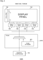
- Fig. 4A is a diagram showing an example of a sub image 900.
- the sub image 900 displayed on the display panel 102 may include multiple segment characters 800.
- description will be made assuming that the sub image 900 has fixed regions R1 through RN each of which is capable of displaying a segment character 800.
- the sub data S3 has no information that specifies the positions of the regions R1 through RN.
- the sub data S3 specifies the character to be displayed for each region R.
- Such an arrangement allows the user of the timing controller 200 to freely display a desired character.
- Fig. 4B is a diagram showing an example of an address map held by the register 214.
- the register of the sub input interface 210 has a 2-byte address area assigned for each region R.
- the address areas 0 to 1 correspond to the region R1
- the address areas 2 to 3 correspond to the region R2.
- the graphic controller 110 writes a value that indicates a character to be displayed, i.e., the sub data S3, to the address that corresponds to each region R.
- the memory 212 stores multiple segment data S4 A through S4 P that each indicate the on/off states of the pixels on the image frame with respect to the corresponding one of the multiple segments (A through P in Fig. 3A ).
- the memory 212 may be configured as nonvolatile memory such as ROM (Read Only Memory) or the like.
- the segment data S4 A represents the on/off state of the segment A
- the segment data S4B represents the on/off state of the segment B. Detailed description will be made later regarding the segment data S4.
- the segment decoder 220 generates a raster image of the segment character 800 to be displayed (conversion into a bitmap format) based on the sub data S3 and the multiple segment data S4.
- the segment decoder 220 outputs output data S5 in the form of image data (sub image data) of the segment character 800 specified by the sub data S3.
- the image processing circuit 204 receives, as input data, the input image data S1 and the sub image data S5 generated by the segment decoder 220.
- the image processing circuit 204 generates the output image data S2 to be displayed on the display panel, based on the input image data S1 and the sub image data S5.
- FIG. 5A is a block diagram showing an example configuration of the image processing circuit 204.
- the image processing circuit 204 may include a multiplexer 205 configured as an input stage to receive the input image data S1 and the sub image data S5, and to select one from among them according to a control signal SEL1.
- a processor 206 configured as a downstream stage performs predetermined signal processing on the image data selected by the multiplexer 205. Before a link is established between the main input interface 202 and the graphic controller 110, the image processing circuit 204 may select the sub image data S5.
- the image processing circuit 204 may select the sub image data S5.
- the image processing circuit 204 selects the input image data S1.
- the image processing circuit 204 may select one from among the input image data S1 and the sub image data S5 according to the control data received from the graphic controller 110.
- the main input interface 202 may be configured to be switched between a mode in which the image data to be displayed is selected from among the input image data S1 and the sub image data S5 and a mode in which the input image data S1 and the sub image data S5 are combined. That is to say, both the functions shown in Fig. 5A and 5B may be implemented.
- the timing controller 200 allows the display panel 102 to display information using desired segment characters specified in a real-time manner according to the sub data S3, instead of or in addition to a predetermined display pattern as shown in Fig. 1 .
- the timing controller 200 is configured to employ such segment characters.
- bitmap information is held for each of multiple alphabetic and numeric characters, e.g., in a case in which each character is represented by (X ⁇ Y)-pixel data
- each character is represented by (X ⁇ Y)-pixel data
- each character is represented by (X ⁇ Y)-pixel data
- the present embodiment requires the timing controller to have only a small memory capacity.
- the present invention encompasses various kinds of apparatuses and circuits that can be regarded as a block configuration or a circuit configuration shown in Fig. 2 , or otherwise that can be derived from the aforementioned description. That is to say, the present invention is not restricted to a specific circuit configuration. More specific description will be made below regarding an example configuration for clarification and ease of understanding of the essence of the present invention and the circuit operation. That is to say, the following description will by no means be intended to restrict the technical scope of the present invention.
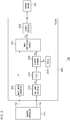
- Fig. 6 is a block diagram showing an example configuration of the segment decoder 220.
- the segment decoder 220 includes a font color generating unit 222, a background color generating unit 224, a multiplexer 226, and a timing generator 228.
- the font color generating unit 222 generates a first luminance value L1 that indicates the color (font color) of the segment character 800.
- the background color generating unit 224 generates a second luminance value L2 that indicates the background color.
- the multiplexer 226 receives the first luminance value L1 and the second luminance value L2. The multiplexer 226 selects one from among the first luminance value L1 and the second luminance value L2 thus received, according to a selection signal SEL2.
- the timing generator 228 controls the multiplexer 226 based on the sub data S3 and the segment data S4. For example, the timing generator 228 converts a sub image represented by the sub data S3 into a raster image, in synchronization with a pixel clock CLK PIX . Such an arrangement requires only a simple configuration to convert such a segment character into a raster image. It should be noted that the configuration of the segment decoder 220 is not restricted to such an arrangement.
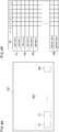
- Figs. 7A and 7B are operation waveform diagrams each showing the operation of the segment decoder 220 shown in Fig. 6 .
- Fig. 7A shows the pixels PIX that form three lines (L i , L i+1 , L i+2 ) to be displayed on the display panel 102. Each pixel included in a segment that is to be turned on is shown in black.
- the timing controller 200 generates RGB data from left-hand pixels to right-hand pixels in every line, from upper lines to lower lines, in synchronization with the pixel clock CLK PIX .
- the timing generator 228 generates the selection signal SEL2 in synchronization with the pixel clock CLK PIX , so as to generate the sub image based on the sub data S3.
- each character is represented by an image including (X ⁇ Y) pixels. Accordingly, each segment data S4 can be represented by (X ⁇ Y)-bit data (in a case in which data compression as described later is not performed).
- the segment character 800 shown in Fig. 3A is designed to have multiple segments that can be classified into groups, each of which is associated with a common shape.
- the segments A, B, P, L, E, and F classified into a first group have a common shape and a position relation in which each segment can be obtained by shifting any one of the other segments in the same group.
- the segments H, J, C, G, N, and D classified into a second group have another common shape.
- the segments I and M classified into a third group have a yet another common shape.
- the segments O and K classified into a fourth group have a yet another common shape.
- the segment data S4 may comprise shape data S7 that represents the shape of the segment and shift data S6 that represents the shift data.
- shape data S7 that represents the shape of the segment
- shift data S6 that represents the shift data.
- Figs. 8A through 8C are diagrams for explaining the segment data compression. Description will be made below directing attention to the first group.
- Fig. 8B shows a common member 804 of the segments A, B, P, L, E, and F, having the same shape, and classified into the first group.
- the common member 804 has a height of y pixels (y ⁇ Y) and a width of x pixels (x ⁇ X), which can be represented by (x ⁇ y)-bit data.
- the shape data S7 is configured as (130 ⁇ 45)-bit data.
- Each of the segments A, B, P, L, F, and E can be represented by the common shape data S7 shifted by ⁇ x in the horizontal direction and by ⁇ y in the vertical direction from a given reference position (x 0 , y 0 ).
- Fig. 8C shows the shift for the segment P.
- the data S6 that represents the shift amount for each segment is configured as (X + Y)-bit data at most.
- the segment data compression is also applicable to the second group through the fourth group in the same way as the first data. It should be noted that the data format of the segment data is not restricted to such an arrangement described above.
- Figs. 9A and 9B are diagrams each showing an in-vehicle display apparatus 600 employing the timing controller 200.
- the in-vehicle display apparatus 600 is embedded in a console 602 in front of a cockpit.
- the in-vehicle display apparatus 600 receives the input image data S1 to be displayed from a vehicle-side processor, and displays a speedometer 604, a tachometer 606 that indicates the rotational speed of an engine, and a remaining fuel meter 608, based on the input image data S1.
- the input image data S1 further includes the remaining battery charge data
- the timing controller 200 further displays a remaining battery charge gauge based the image data S1 ( Fig. 9A ).
- the in-vehicle display apparatus 600 when the in-vehicle display apparatus 600 is started up after the user switches on the ignition, such an arrangement allows a given character string such as "PLEASE WAIT", a character string that represents the current time, or the like, to be displayed in the form of the sub image data S5 before the input image data S1 can be displayed.
- a given character string such as "PLEASE WAIT", a character string that represents the current time, or the like
- the timing controller 200 may be employed in a medical display apparatus.
- the medical display apparatus displays necessary information for medical doctors and nurses in a medical examination, medical treatment, or surgery.
- the timing controller 200 allows such a medical display apparatus to display important information (e.g., the heart rate, blood pressure, and the like, of the subject) in the form of the sub image data S5 even in a situation in which the input image data S1 cannot be displayed.
- Fig. 10 is a perspective view showing an electronic device 500.
- the electronic device 500 shown in Fig. 10 may be configured as a laptop PC, a tablet terminal, a smartphone, a portable game machine, an audio player, or the like.
- the electronic device 500 includes a graphic controller 110, a display panel 102, a gate driver 104, and a source driver 106, each of which is built into a housing 502.
- a transmission apparatus 120 may be arranged between the timing controller 200 and the graphic controller 110, and may include a differential transmitter, a propagation path, and a differential receiver.
- Fig. 11 is a block diagram showing a part of a configuration of a timing controller 200a according to a first modification.
- the sub data S3' received from the graphic controller 110 includes a character code that specifies a segment character.
- the character code thus employed may be configured as an ASCII (American Standard Code for Information Interchange) code.
- the segment decoder 220 of the timing controller 200a further includes a character decoder 230 that converts a given character code into multiple bits that indicate the on/off states of the multiple segments.
- Fig. 12 is a block diagram showing a part of a configuration of a timing controller 200b according to a second modification.
- the timing controller 200b further includes an image generating unit 232 that generates local sub data S3b.
- the image generating unit 232 writes the sub data S3b to the register 214.
- the sub data to be written to the register 214 is selected from among the external sub data S3a input to the sub input interface 210 from an external circuit and the local sub data S3b generated by an internal component of the timing controller 200b.
- the sub data thus selected is written to the register 214.
- the segment decoder 220b converts a given segment character into a raster image based on the sub data written to the register 214. This allows debug information and error information with respect to the timing controller 200b itself to be displayed.
- the configuration of the sub input interface 210 is not restricted to such a register access-type configuration.
- the sub input interface 210 may be configured to employ differential serial transmission as with the first line 112.
- the sub input interface 210 may be designed as a desired interface.
- each segment character 800 may have a font size that can be selected from among multiple font sizes.
- the segment data S4 may preferably be prepared for each font size, and the sub data S3 may preferably include additional data for specifying the font size.
- an arrangement may be made which is capable of specifying the drawing position for each of the multiple segment characters 800. That is to say, an arrangement may be made which is capable of changing the coordinate position for each of the multiple regions R1 through RN.
- the sub data S3 may include data that indicates the character interval. Description has been made with reference to Fig. 4A regarding an arrangement in which the sub image 900 is configured as a single line. Also, the sub image 900 may be configured as multiple-line text.
- the sub data S3 may include a parameter that indicates the alignment in the height direction for each of the multiple segment characters 800 to be drawn on a single line, examples of which include the bottom alignment, top alignment, center alignment, and the like.
- the sub data S3 may further include third data that indicates the transparency of the segment character.
- a pixel sequence that corresponds to the main image may be input as the second luminance value L2 shown in Fig. 6 .
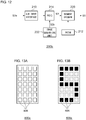
- Figs. 13A and 13B are diagrams each showing a segment character according to a seventh modification.
- Such a segment character 800a is configured as a dot-matrix character formed of multiple dots 806.
- Fig. 13 shows a (4 ⁇ 7)-dot matrix.
- the number of dots in each of the vertical direction and horizontal direction is not restricted in particular. It can be assumed that the multiple dots 806 are equivalent to the multiple segments 802.
- each dot 806 is not equivalent to a single pixel of the display panel 102. Rather, each dot 806 includes multiple pixels.
- the shape of each dot 806 is not restricted to such a rectangular shape. Also, each dot 806 may have other shapes such as a circular shape, a rhombic shape, an octagonal shape, or the like.
- the memory 212 stores multiple segment data each of which specifies the on/off states of the pixels on an image frame for each of the multiple dots 806.
- the multiple dots 806 may be configured to have the same shape. Such an arrangement allows the segment data to be compressed using the method described with reference to Figs. 8A through 8C .
- Each (4 ⁇ 7)-dot matrix character can be represented by 28-bit data. Accordingly, by preparing a 4-byte (32-bit) register (214 in Fig. 2 ) for each character, such an arrangement is capable of uniquely specifying a given character or symbol to be displayed.
- Figs. 14A and 14B are diagrams each showing a segment character according to an eighth modification.
- Fig. 14A shows "A" as an upper-case letter of the alphabet.
- Fig. 14B shows "C” as an upper-case letter of the alphabet.
- each segment character is configured as a combination of multiple types of segments (four types in this example, i.e., segment types A through D).
- the shape of each segment is not restricted to such a rectangular shape.
- each segment data S4 corresponds to the multiple types of segments.
- Each segment data S4 specifies the shape of the corresponding segment type (which is represented by the on/off states of the pixels on the image frame, for example).
- the data for representing each segment character includes: (i) type data that specifies the segment type for each of the multiple segments to be used; and (ii) position data that specifies the position of each of the multiple segments to be used.
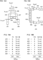
- Fig. 15A is a diagram showing description data S30[A] that represents the segment character "A” shown in Fig. 14A.
- Fig. 15B is a diagram showing description data S30[C] that represents the segment character "C” shown in Fig. 14B .
- the segment character 300 shown in Fig. 14A is formed of eight segments 301 through 308. Accordingly, the description data S30[A] thereof includes type data S31 that specifies the respective types of the eight segments 301 through 308 and position data S32 that specifies the respective positions of the eight segments 301 through 308. The position may be represented by the coordinate position of the upper-left corner of each segment or otherwise any one of the other corners.
- a segment character 400 shown in Fig. 15A is formed of eight segments 401 through 408. Accordingly, the description data S30[C] thereof includes the type data S31 that specifies the respective types of the eight segments 401 through 408 and the position data S32 that specifies the respective positions of the eight segments 401 through 408.
- the description data S30 may preferably be defined for each character to be used.
- the upper-case letters of the alphabet "A” through “Z” may be represented by defining 26 sets of description data S30[A] through S30[Z].
- the lower-case letters of the alphabet "a” through “z” may be represented by defining 26 sets of description data S30[a] through S30[z].
- the numerals "0" through “9” may be represented by defining ten sets of description data S30[0] through S30[9].
- Greek letters, Japanese hiragana characters, Japanese katakana characters, and Chinese characters may be defined.
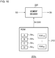
- Fig. 16 is a diagram showing a part of a timing controller 200c according to an eighth modification.
- the memory 212 stores the type data S30 defined for each segment character in addition to the segment data S4 defined for each segment type.
- the segment decoder 220 receives the sub data S3 that specifies the segment character to be displayed, and reads out the description data S30 that corresponds to the segment character to be displayed.
- the sub data S3 indicates an instruction to display the letter of the alphabet "A”
- such an arrangement assigns a segment of the type A to the coordinate position (x1, y1) as the segment 301 based on the type data S30[A] shown in Fig. 15A .
- such an arrangement assigns a segment of the type A to the coordinate position (x2, y2) as the segment 302.
- Such an arrangement allows desired characters and symbols to be displayed.
Landscapes
- Engineering & Computer Science (AREA)
- Physics & Mathematics (AREA)
- Computer Hardware Design (AREA)
- General Physics & Mathematics (AREA)
- Theoretical Computer Science (AREA)
- Chemical & Material Sciences (AREA)
- Crystallography & Structural Chemistry (AREA)
- Control Of Indicators Other Than Cathode Ray Tubes (AREA)
- Controls And Circuits For Display Device (AREA)
- Digital Computer Display Output (AREA)
Applications Claiming Priority (2)
| Application Number | Priority Date | Filing Date | Title |
|---|---|---|---|
| JP2016018702 | 2016-02-03 | ||
| JP2016083131A JP6698412B2 (ja) | 2016-02-03 | 2016-04-18 | タイミングコントローラ、それを用いた電子機器、車載用または医療用ディスプレイ装置 |
Publications (2)
| Publication Number | Publication Date |
|---|---|
| EP3203461A2 true EP3203461A2 (de) | 2017-08-09 |
| EP3203461A3 EP3203461A3 (de) | 2017-08-23 |
Family
ID=57956135
Family Applications (1)
| Application Number | Title | Priority Date | Filing Date |
|---|---|---|---|
| EP17153988.5A Ceased EP3203461A3 (de) | 2016-02-03 | 2017-01-31 | Zeitgeber |
Country Status (2)
| Country | Link |
|---|---|
| US (1) | US10235931B2 (de) |
| EP (1) | EP3203461A3 (de) |
Families Citing this family (5)
| Publication number | Priority date | Publication date | Assignee | Title |
|---|---|---|---|---|
| JP7149058B2 (ja) * | 2017-08-10 | 2022-10-06 | ローム株式会社 | 車載用のタイミングコントローラおよびそれを用いた自動車 |
| AU2021307935A1 (en) | 2020-07-16 | 2023-03-16 | Ventec Life Systems, Inc. | System and method for concentrating gas |
| US11915570B2 (en) | 2020-07-16 | 2024-02-27 | Ventec Life Systems, Inc. | System and method for concentrating gas |
| CA3189540A1 (en) | 2020-07-16 | 2022-01-20 | Invacare Corporation | System and method for concentrating gas |
| EP4181995A4 (de) | 2020-07-16 | 2025-05-07 | Ventec Life Systems, Inc. | System und verfahren zur konzentration von gas |
Citations (7)
| Publication number | Priority date | Publication date | Assignee | Title |
|---|---|---|---|---|
| JPS6211886A (ja) * | 1985-07-10 | 1987-01-20 | 株式会社日立製作所 | 漢字パタ−ン発生器 |
| JPH06138866A (ja) * | 1992-10-30 | 1994-05-20 | Nec Ic Microcomput Syst Ltd | 文字フォント生成装置ならびに文字フォント生成方法 |
| JPH06317782A (ja) | 1993-03-25 | 1994-11-15 | Toshiba Corp | 表示装置 |
| JP2002169524A (ja) | 2000-12-01 | 2002-06-14 | Sony Corp | 通信方法および装置、ならびに、表示方法および装置 |
| US20050177787A1 (en) * | 2003-10-01 | 2005-08-11 | Yvonne Yen | Method and apparatus for font processing |
| US6995779B1 (en) * | 1998-01-29 | 2006-02-07 | Rohm Co., Ltd. | Driving device for a display |
| WO2007130049A1 (en) * | 2006-05-05 | 2007-11-15 | Panasonic Automotive Systems Company Of America Division Of Panasonic Corporation Of North America | System and method for adding on-screen display information into a video signal |
Family Cites Families (5)
| Publication number | Priority date | Publication date | Assignee | Title |
|---|---|---|---|---|
| US4513282A (en) * | 1979-12-28 | 1985-04-23 | Citizen Watch Company Limited | Liquid crystal matrix display device |
| US4533909A (en) * | 1980-05-16 | 1985-08-06 | Apple Computer, Inc. | Computer with color display |
| BR9909213A (pt) * | 1998-12-15 | 2000-11-14 | Citizen Watch Co Ltd | Dispositivo eletrônico |
| JP2009032714A (ja) * | 2007-07-24 | 2009-02-12 | Renesas Technology Corp | 半導体集積回路、表示装置及び電子回路 |
| JP4995325B2 (ja) * | 2008-07-25 | 2012-08-08 | 株式会社アドバンテスト | クロック乗せ換え回路およびそれを用いた試験装置 |
-
2017
- 2017-01-31 EP EP17153988.5A patent/EP3203461A3/de not_active Ceased
- 2017-02-01 US US15/422,007 patent/US10235931B2/en active Active
Patent Citations (7)
| Publication number | Priority date | Publication date | Assignee | Title |
|---|---|---|---|---|
| JPS6211886A (ja) * | 1985-07-10 | 1987-01-20 | 株式会社日立製作所 | 漢字パタ−ン発生器 |
| JPH06138866A (ja) * | 1992-10-30 | 1994-05-20 | Nec Ic Microcomput Syst Ltd | 文字フォント生成装置ならびに文字フォント生成方法 |
| JPH06317782A (ja) | 1993-03-25 | 1994-11-15 | Toshiba Corp | 表示装置 |
| US6995779B1 (en) * | 1998-01-29 | 2006-02-07 | Rohm Co., Ltd. | Driving device for a display |
| JP2002169524A (ja) | 2000-12-01 | 2002-06-14 | Sony Corp | 通信方法および装置、ならびに、表示方法および装置 |
| US20050177787A1 (en) * | 2003-10-01 | 2005-08-11 | Yvonne Yen | Method and apparatus for font processing |
| WO2007130049A1 (en) * | 2006-05-05 | 2007-11-15 | Panasonic Automotive Systems Company Of America Division Of Panasonic Corporation Of North America | System and method for adding on-screen display information into a video signal |
Also Published As
| Publication number | Publication date |
|---|---|
| EP3203461A3 (de) | 2017-08-23 |
| US20170221414A1 (en) | 2017-08-03 |
| US10235931B2 (en) | 2019-03-19 |
Similar Documents
| Publication | Publication Date | Title |
|---|---|---|
| JP6698412B2 (ja) | タイミングコントローラ、それを用いた電子機器、車載用または医療用ディスプレイ装置 | |
| US10235931B2 (en) | Timing controller | |
| US11186294B2 (en) | In-vehicle timing controller and vehicle using the same | |
| US6266042B1 (en) | Display system with resolution conversion | |
| US11250766B2 (en) | Semiconductor apparatus | |
| KR101987186B1 (ko) | 멀티비젼 시스템 및 그 구동방법 | |
| KR20060047943A (ko) | 표시 패널 구동장치 | |
| CN113314082B (zh) | 显示装置以及源极驱动器 | |
| US10068536B2 (en) | Circuit device, electro-optical device, and electronic apparatus | |
| CN107665105A (zh) | 显示设备接口转换装置、多屏显示系统及多屏显示方法 | |
| JP7097507B2 (ja) | 半導体装置、それを用いた車載用ディスプレイシステム、電子機器 | |
| US6483510B1 (en) | Integrated graphic and character mixing circuit for driving an LCD display | |
| US9305510B2 (en) | LCD driving module, LCD device, and method for driving LCD | |
| US11367415B2 (en) | Semiconductor apparatus | |
| US20200242989A1 (en) | Electro-optical apparatus, display control system, display driver, electronic device, and mobile unit | |
| CN117734427A (zh) | 控制器电路及车载显示系统 | |
| KR20040038665A (ko) | 표시 유닛, 표시 장치, 및 화상 표시 시스템 | |
| JP2008209711A (ja) | 電子ペーパー | |
| JP4698139B2 (ja) | 画像表示装置及びマルチディスプレイ装置 | |
| US20030179179A1 (en) | Apparatus, method and program for generating image signal having pointer signal | |
| US20190193562A1 (en) | Display system and driving method thereof | |
| US11715442B2 (en) | Semiconductor apparatus with OSD function | |
| US11074843B2 (en) | Drive circuit, electro-optical device, electronic apparatus including electro-optical device, and movable body including electronic apparatus | |
| CN212570348U (zh) | 一种多屏显示检测装置 | |
| JP2025099469A (ja) | 半導体装置および表示システム |
Legal Events
| Date | Code | Title | Description |
|---|---|---|---|
| PUAI | Public reference made under article 153(3) epc to a published international application that has entered the european phase |
Free format text: ORIGINAL CODE: 0009012 |
|
| STAA | Information on the status of an ep patent application or granted ep patent |
Free format text: STATUS: THE APPLICATION HAS BEEN PUBLISHED |
|
| PUAL | Search report despatched |
Free format text: ORIGINAL CODE: 0009013 |
|
| AK | Designated contracting states |
Kind code of ref document: A2 Designated state(s): AL AT BE BG CH CY CZ DE DK EE ES FI FR GB GR HR HU IE IS IT LI LT LU LV MC MK MT NL NO PL PT RO RS SE SI SK SM TR |
|
| AX | Request for extension of the european patent |
Extension state: BA ME |
|
| AK | Designated contracting states |
Kind code of ref document: A3 Designated state(s): AL AT BE BG CH CY CZ DE DK EE ES FI FR GB GR HR HU IE IS IT LI LT LU LV MC MK MT NL NO PL PT RO RS SE SI SK SM TR |
|
| AX | Request for extension of the european patent |
Extension state: BA ME |
|
| RIC1 | Information provided on ipc code assigned before grant |
Ipc: G09G 3/20 20060101AFI20170719BHEP Ipc: G09G 5/22 20060101ALI20170719BHEP |
|
| STAA | Information on the status of an ep patent application or granted ep patent |
Free format text: STATUS: REQUEST FOR EXAMINATION WAS MADE |
|
| 17P | Request for examination filed |
Effective date: 20180223 |
|
| RBV | Designated contracting states (corrected) |
Designated state(s): AL AT BE BG CH CY CZ DE DK EE ES FI FR GB GR HR HU IE IS IT LI LT LU LV MC MK MT NL NO PL PT RO RS SE SI SK SM TR |
|
| STAA | Information on the status of an ep patent application or granted ep patent |
Free format text: STATUS: EXAMINATION IS IN PROGRESS |
|
| 17Q | First examination report despatched |
Effective date: 20180524 |
|
| STAA | Information on the status of an ep patent application or granted ep patent |
Free format text: STATUS: THE APPLICATION HAS BEEN REFUSED |
|
| 18R | Application refused |
Effective date: 20191202 |