EP3203523B1 - Méthode d'affichage pour une structure de pixel - Google Patents
Méthode d'affichage pour une structure de pixel Download PDFInfo
- Publication number
- EP3203523B1 EP3203523B1 EP15793668.3A EP15793668A EP3203523B1 EP 3203523 B1 EP3203523 B1 EP 3203523B1 EP 15793668 A EP15793668 A EP 15793668A EP 3203523 B1 EP3203523 B1 EP 3203523B1
- Authority
- EP
- European Patent Office
- Prior art keywords
- sub
- pixel
- pixels
- adjacent
- display
- Prior art date
- Legal status (The legal status is an assumption and is not a legal conclusion. Google has not performed a legal analysis and makes no representation as to the accuracy of the status listed.)
- Active
Links
Images


Classifications
-
- G—PHYSICS
- G09—EDUCATION; CRYPTOGRAPHY; DISPLAY; ADVERTISING; SEALS
- G09G—ARRANGEMENTS OR CIRCUITS FOR CONTROL OF INDICATING DEVICES USING STATIC MEANS TO PRESENT VARIABLE INFORMATION
- G09G3/00—Control arrangements or circuits, of interest only in connection with visual indicators other than cathode-ray tubes
- G09G3/20—Control arrangements or circuits, of interest only in connection with visual indicators other than cathode-ray tubes for presentation of an assembly of a number of characters, e.g. a page, by composing the assembly by combination of individual elements arranged in a matrix no fixed position being assigned to or needed to be assigned to the individual characters or partial characters
- G09G3/2003—Display of colours
-
- G—PHYSICS
- G02—OPTICS
- G02F—OPTICAL DEVICES OR ARRANGEMENTS FOR THE CONTROL OF LIGHT BY MODIFICATION OF THE OPTICAL PROPERTIES OF THE MEDIA OF THE ELEMENTS INVOLVED THEREIN; NON-LINEAR OPTICS; FREQUENCY-CHANGING OF LIGHT; OPTICAL LOGIC ELEMENTS; OPTICAL ANALOGUE/DIGITAL CONVERTERS
- G02F1/00—Devices or arrangements for the control of the intensity, colour, phase, polarisation or direction of light arriving from an independent light source, e.g. switching, gating or modulating; Non-linear optics
- G02F1/01—Devices or arrangements for the control of the intensity, colour, phase, polarisation or direction of light arriving from an independent light source, e.g. switching, gating or modulating; Non-linear optics for the control of the intensity, phase, polarisation or colour
- G02F1/13—Devices or arrangements for the control of the intensity, colour, phase, polarisation or direction of light arriving from an independent light source, e.g. switching, gating or modulating; Non-linear optics for the control of the intensity, phase, polarisation or colour based on liquid crystals, e.g. single liquid crystal display cells
- G02F1/133—Constructional arrangements; Operation of liquid crystal cells; Circuit arrangements
- G02F1/136—Liquid crystal cells structurally associated with a semi-conducting layer or substrate, e.g. cells forming part of an integrated circuit
- G02F1/1362—Active matrix addressed cells
-
- G—PHYSICS
- G09—EDUCATION; CRYPTOGRAPHY; DISPLAY; ADVERTISING; SEALS
- G09G—ARRANGEMENTS OR CIRCUITS FOR CONTROL OF INDICATING DEVICES USING STATIC MEANS TO PRESENT VARIABLE INFORMATION
- G09G3/00—Control arrangements or circuits, of interest only in connection with visual indicators other than cathode-ray tubes
- G09G3/20—Control arrangements or circuits, of interest only in connection with visual indicators other than cathode-ray tubes for presentation of an assembly of a number of characters, e.g. a page, by composing the assembly by combination of individual elements arranged in a matrix no fixed position being assigned to or needed to be assigned to the individual characters or partial characters
- G09G3/22—Control arrangements or circuits, of interest only in connection with visual indicators other than cathode-ray tubes for presentation of an assembly of a number of characters, e.g. a page, by composing the assembly by combination of individual elements arranged in a matrix no fixed position being assigned to or needed to be assigned to the individual characters or partial characters using controlled light sources
- G09G3/30—Control arrangements or circuits, of interest only in connection with visual indicators other than cathode-ray tubes for presentation of an assembly of a number of characters, e.g. a page, by composing the assembly by combination of individual elements arranged in a matrix no fixed position being assigned to or needed to be assigned to the individual characters or partial characters using controlled light sources using electroluminescent panels
- G09G3/32—Control arrangements or circuits, of interest only in connection with visual indicators other than cathode-ray tubes for presentation of an assembly of a number of characters, e.g. a page, by composing the assembly by combination of individual elements arranged in a matrix no fixed position being assigned to or needed to be assigned to the individual characters or partial characters using controlled light sources using electroluminescent panels semiconductive, e.g. using light-emitting diodes [LED]
- G09G3/3208—Control arrangements or circuits, of interest only in connection with visual indicators other than cathode-ray tubes for presentation of an assembly of a number of characters, e.g. a page, by composing the assembly by combination of individual elements arranged in a matrix no fixed position being assigned to or needed to be assigned to the individual characters or partial characters using controlled light sources using electroluminescent panels semiconductive, e.g. using light-emitting diodes [LED] organic, e.g. using organic light-emitting diodes [OLED]
-
- H—ELECTRICITY
- H10—SEMICONDUCTOR DEVICES; ELECTRIC SOLID-STATE DEVICES NOT OTHERWISE PROVIDED FOR
- H10K—ORGANIC ELECTRIC SOLID-STATE DEVICES
- H10K50/00—Organic light-emitting devices
-
- H—ELECTRICITY
- H10—SEMICONDUCTOR DEVICES; ELECTRIC SOLID-STATE DEVICES NOT OTHERWISE PROVIDED FOR
- H10K—ORGANIC ELECTRIC SOLID-STATE DEVICES
- H10K59/00—Integrated devices, or assemblies of multiple devices, comprising at least one organic light-emitting element covered by group H10K50/00
- H10K59/30—Devices specially adapted for multicolour light emission
- H10K59/35—Devices specially adapted for multicolour light emission comprising red-green-blue [RGB] subpixels
- H10K59/353—Devices specially adapted for multicolour light emission comprising red-green-blue [RGB] subpixels characterised by the geometrical arrangement of the RGB subpixels
-
- H—ELECTRICITY
- H10—SEMICONDUCTOR DEVICES; ELECTRIC SOLID-STATE DEVICES NOT OTHERWISE PROVIDED FOR
- H10P—GENERIC PROCESSES OR APPARATUS FOR THE MANUFACTURE OR TREATMENT OF DEVICES COVERED BY CLASS H10
- H10P14/00—Formation of materials, e.g. in the shape of layers or pillars
- H10P14/60—Formation of materials, e.g. in the shape of layers or pillars of insulating materials
- H10P14/61—Formation of materials, e.g. in the shape of layers or pillars of insulating materials using masks
-
- G—PHYSICS
- G02—OPTICS
- G02F—OPTICAL DEVICES OR ARRANGEMENTS FOR THE CONTROL OF LIGHT BY MODIFICATION OF THE OPTICAL PROPERTIES OF THE MEDIA OF THE ELEMENTS INVOLVED THEREIN; NON-LINEAR OPTICS; FREQUENCY-CHANGING OF LIGHT; OPTICAL LOGIC ELEMENTS; OPTICAL ANALOGUE/DIGITAL CONVERTERS
- G02F2201/00—Constructional arrangements not provided for in groups G02F1/00 - G02F7/00
- G02F2201/52—RGB geometrical arrangements
-
- G—PHYSICS
- G09—EDUCATION; CRYPTOGRAPHY; DISPLAY; ADVERTISING; SEALS
- G09G—ARRANGEMENTS OR CIRCUITS FOR CONTROL OF INDICATING DEVICES USING STATIC MEANS TO PRESENT VARIABLE INFORMATION
- G09G2300/00—Aspects of the constitution of display devices
- G09G2300/04—Structural and physical details of display devices
- G09G2300/0439—Pixel structures
- G09G2300/0452—Details of colour pixel setup, e.g. pixel composed of a red, a blue and two green components
-
- G—PHYSICS
- G09—EDUCATION; CRYPTOGRAPHY; DISPLAY; ADVERTISING; SEALS
- G09G—ARRANGEMENTS OR CIRCUITS FOR CONTROL OF INDICATING DEVICES USING STATIC MEANS TO PRESENT VARIABLE INFORMATION
- G09G2300/00—Aspects of the constitution of display devices
- G09G2300/04—Structural and physical details of display devices
- G09G2300/0439—Pixel structures
- G09G2300/0465—Improved aperture ratio, e.g. by size reduction of the pixel circuit, e.g. for improving the pixel density or the maximum displayable luminance or brightness
-
- G—PHYSICS
- G09—EDUCATION; CRYPTOGRAPHY; DISPLAY; ADVERTISING; SEALS
- G09G—ARRANGEMENTS OR CIRCUITS FOR CONTROL OF INDICATING DEVICES USING STATIC MEANS TO PRESENT VARIABLE INFORMATION
- G09G2320/00—Control of display operating conditions
- G09G2320/02—Improving the quality of display appearance
- G09G2320/0242—Compensation of deficiencies in the appearance of colours
Definitions
- the present invention belongs to the technical field of display, and specifically relates to a display method of a pixel structure.
- the color display screen displays an image by means of pixel units.
- a pixel unit includes sub-pixels with three different colors of red(R), green(G) and blue(B), and the color and brightness displayed in a pixel point (wherein each pixel point corresponds to one pixel unit) are controlled by means of controlling magnitudes of components of three RGB sub-pixels in corresponding pixel unit.
- Figs. 1A to 1C are structural schematic diagrams of arrangements of the RGB sub-pixels in a pixel unit in the related art, including the following three types of arrangement: bar-shape arrangement (see Fig. 1A ), delta arrangement (see Fig. 1B ) and mosaic arrangement (see Fig. 1C ).
- the RGB sub-pixels are arranged in rows sequentially and the same type of RGB sub-pixels are arranged in a column respectively. Since there is only one color in the direction of column in such an arrangement, the color nonuniformity and the error of color edge are readily to occur, affecting the display effect.
- the color nonuniformity in some directions also occurs and the resolution therein is not high.
- the resolution of a display device can be improved by increasing Pixels Per Inch (PPI) of the display device.
- PPI Pixels Per Inch
- each pixel consists of sub-pixels, the number of needed sub-pixels is large when a display device requires a large amount of pixels to achieve the display with high resolution.
- the improvement to the process will reach the limits with consistent refinement of the process.
- EP 2709155 A1 and EP2637209 A1 provide a pixel arrangement structure to improve aperture ratio of pixels by efficiently setting up the gaps between pixels.
- the pixel arrangement structure includes a first pixel having a center coinciding with a center of a virtual square; a second pixel separated from the first pixel and having a center at a first vertex of the virtual square; and a third pixel separated from the first pixel and the second pixel, and having a center at a second vertex neighboring the first vertex of the virtual square.
- the first pixel, the second pixel, and the third pixel have polygonal shapes.
- the first pixel has an octagonal shape, and at least one of the second pixel or the third pixel has a hexagonal shape.
- CN103745684 A discloses a pixel array, a display and a method for rendering image on the display.
- the pixel array is composed of a plurality of basic pixel units arranged in row and column directions.
- Each of the basic pixel units comprises: a first sub-pixel group composed of two adjacent first type sub-pixels having a first color, with a distance therebetween smaller than a first predetermined value; a second sub-pixel group composed of two adjacent second type sub-pixels having a second color, with a distance therebetween smaller than the first predetermined value; and two third sub-pixel groups, each of which is composed of two adjacent third type sub-pixels having a third color, with a distance therebetween smaller than the first predetermined value.
- US 2007/257946A1 discloses a full-color display system having improved apparent resolution.
- the full-color display system comprises a display formed from an array of full-color groups of light-emitting elements each comprising more than one luma-chroma sub-group of light-emitting elements; and a processor for receiving a full color input image signal that specifies full color image values at each of a two-dimensional number of sampled addressable spatial locations within an image to be displayed, for providing a full color image signal with image signal values corresponding to the spatial location of each luma-chroma sub-group, for computing a control signal representing the relative values, or difference between values, for the image signal values corresponding to each luma-chroma sub-group and at least one of each luma-chroma sub-group's neighbors, and for rendering a signal for driving each light-emitting element within each luma-chroma sub-group of light-emitting elements as a function of the values for the image signal corresponding to each lum
- CN103956134 A discloses a display method wherein subpixels are borrowed by pixel units to display an image.
- US2014/252321 A1 discloses a pixel structure having first and second pixel units comprising subpixels arranged in an oblique line.
- an object of the present invention is to provide a display method of a pixel structure, the pixel structure capable of increasing the aperture ratios of sub-pixels while achieving high resolution, which not only simplifies the manufacture process, obtains good brightness level and extends the lifetime of product, but also prevents the error of color edge and the color nonuniformity by setting the weighted value of the missing basic color of the pixel structure in the display process, hence achieving better display effect.
- the technical solution used to solve the technical problem in the present invention is the display method of the pixel structure described in claim 1.
- Area of the second sub-pixel is the same as that of the fourth sub-pixel, and area of the first sub-pixel is the same as that of the third sub-pixel and greater than that of the second sub-pixel.
- the distance between two adjacent second sub-pixels is equal to the distance between two adjacent fourth sub-pixels, and less than the distance between two adjacent first sub-pixels and the distance between two adjacent third sub-pixels.
- the distance between the first sub-pixel and the third sub-pixel adjacent to each other is less than the distance between the second sub-pixel and the fourth sub-pixel adjacent to each other.
- the first sub-pixel and the second sub-pixel in the first pixel unit are disposed in adjacent two rows and adjacent two columns of sub-pixels
- the third sub-pixel and the fourth sub-pixel in the second pixel unit are disposed in adjacent two rows and adjacent two columns of sub-pixels, so that the first sub-pixels and the third sub-pixels are arranged alternately in turn in the row or column direction respectively, and the second sub-pixels and the fourth sub-pixels are arranged alternately in turn in the row or column direction, respectively.
- first sub-pixels and the third sub-pixels are alternately disposed in odd rows and odd columns, and the second sub-pixels and the fourth sub-pixels are alternately disposed in even rows and even columns; or,
- centers of the first sub-pixels and the third sub-pixels located in the same row or column are in the same line, and centers of the second sub-pixels and the fourth sub-pixels located in the same row or column are in the same line.
- the first sub-pixels, the second sub-pixels, the third sub-pixels and the fourth sub-pixels are arranged uniformly.
- the center of the first sub-pixel is located in the perpendicular bisector of a line connecting the centers of two third sub-pixels adjacent to the first sub-pixel; and in the same row, the center of the first sub-pixel is located in the perpendicular bisector of a line connecting the centers of two third sub-pixels adjacent to the first sub-pixel.
- the center of the third sub-pixel is located in the perpendicular bisector of a line connecting the centers of two first sub-pixels adjacent to the third sub-pixel; and in the same row, the center of the third sub-pixel is located in the perpendicular bisector of a line connecting the centers of two first sub-pixels adjacent to the third sub-pixel.
- the second sub-pixel or the fourth sub-pixel is located in a direction of an oblique angle of 45 degree with respect to the first sub-pixel or the third sub-pixel.
- distance between the first sub-pixel and the second sub-pixel adjacent to each other is equal to distance between the third sub-pixel and the fourth sub-pixel adjacent to each other, and distance between the first sub-pixel and the third sub-pixel adjacent to each other is less than distance between the second sub-pixel and the fourth sub-pixel adjacent to each other.
- the basic colors include red, green and blue, the basic color of the first sub-pixel is red, the basic color of the third sub-pixel is blue, and the basic colors of the second and the fourth sub-pixels are green.
- the shapes of the first sub-pixel, the second sub-pixel, the third sub-pixel and the fourth sub-pixel are any one of round shape, triangular shape, quadrangular shape different from a square shape or diamond shape, pentagonal shape, hexagonal shape or octagonal shape or a combination thereof.
- the shapes of the first sub-pixel and the third sub-pixel are the same, and the shapes of the first sub-pixel and the third sub-pixel are the same.
- the first sub-pixel and the second sub-pixel in the first pixel unit are connected to one data line respectively, and the third sub-pixel and fourth sub-pixel in the second pixel unit are connected to one data line respectively, the data lines being used to receive the pixel display information.
- the display device is an organic light emission diode display device or liquid crystal display device.
- the advantageous effects of the present invention are in that the pixel structure and the display method thereof provided in the present invention increases the aperture ratios of sub-pixels by improving the pixel arrangement, and increases the brightness of pixel structure and the pixel resolution correspondingly; in the meantime, a display method with respect to the above pixel structure is designed, which is capable of implementing normal image display and preventing the error of color edge and the color nonuniformity due to the pixel arrangements in the related art, thereby improving the display effect of display devices and solving the problems that the resolution of a display device, especially of an organic light emission display device, is hard to improve due to the process issue in the related art.
- the technical concept of the present invention is: forming a plurality of colors by using the mixture of three primary colors of red, green and blue so as to implement the image display; and disposing the three primary colors of red, green and blue, which are disposed in the same pixel unit in the related art, separately into adjacent two pixel units by using the characteristics that the sensitivity of human eyes to different colors varies, and adjusting the arrangement of pixel units such that the pixel unit in the pixel structure can implement the display of three primary colors of RGB by additionally using the missing basic colors of its own from adjacent pixel units, therefore implementing the image display with different colors and obtaining good color uniformity.
- a pixel structure includes first pixel units and second pixel units arranged alternately in turn, wherein the first pixel unit comprises a first sub-pixel and a second sub-pixel arranged in an oblique line, and the second pixel unit comprises a third sub-pixel and a fourth sub-pixel arranged in an oblique line; and the first and the third sub-pixels have different basic colors and the second and the fourth sub-pixels have the same basic color.
- Such pixel structure is capable of increasing the aperture ratio of sub-pixels while achieving high resolution, which not only simplifies the manufacture process, obtains good brightness level and extends the lifetime of the product, but also prevents the error of color edge and the color nonuniformity by setting the weighted value of the missing basic color of the pixel structure in the display process, hence achieving better display effect.
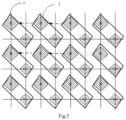
- this embodiment provides a pixel structure, including first pixel units 1 and second pixel units 2 which are arranged alternately in turn, wherein the first pixel unit 1 comprises a first sub-pixel 11 and a second sub-pixel 12 arranged in an oblique line, and the second pixel unit 2 comprises a third sub-pixel 21 and a fourth sub-pixel 22 arranged in an oblique line; and the first sub-pixel 11 and the third sub-pixel 21 have different basic colors, and the second sub-pixel 12 and the fourth sub-pixel 22 have the same basic color.
- the basic color of the first sub-pixel 11 is red
- the basic color of the third sub-pixel 21 is blue
- the basic color of the second sub-pixel 12 and the fourth sub-pixel 22 is green.
- the basic color refers to color owned by the sub-pixel structure and capable of implementing the color display.
- the basic color refers to the color of the light-emitting layer in the organic light emitting diode, that is, the color corresponding to the light emitted from the light-emitting layer under normal voltage; with respect to the pixel structure in the liquid crystal display device, the basic color refers to color of a color filter (referred to as CF) in a color filter substrate, that is, the color corresponding to the light of the backlight source which is filtered by the color filter substrate.
- the basic colors include red, green and blue.
- the basic color of sub-pixel may be selected any one from the three primary colors of red, green and blue.
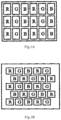
- alternating arrangements of the first and the second pixel units are shown in Figs. 2A and 2B , in which the directions of the oblique arrangements of the sub-pixels in the first pixel unit 1 and the second pixel unit 2 adjacent to each other in each column may parallel to each other (as shown in Fig. 2A ), or may cross each other and even may be perpendicular to each other (as shown in Fig. 2B ).
- the first pixel units 1 and the second pixel units 2 are alternately arranged in the row and column directions. Specifically, the first pixel units 1 and the second pixel units 2 are alternately arranged in the row and column directions. Among the pixel units in adjacent rows, the first pixel unit 1 and the second pixel unit 2 are arranged to stagger one pixel unit distance in the row direction. Among the pixel units in adjacent columns, the first pixel unit 1 and the second pixel unit 2 are arranged to stagger one pixel unit distance in the column direction.
- the pixel unit include the first pixel unit 1 or the second pixel unit 2.
- the first pixel units 1 and the second pixel units 2 are arranged in a different order in adjacent rows of pixel units as well as in adjacent columns of pixel units. As shown in Figs. 2A and 2B , each pixel unit is illustrated in the dash-line frame. Among two adjacent rows of the pixel units, if the first pixel units 1 and the second pixel units 2 in one row are arranged in the order of the first pixel unit 1, the second pixel unit 2, the first pixel unit 1, the second pixel unit 2, ..., the first pixel units 1 and the second pixel units 2 in the other row are arranged in the order of the second pixel unit 2, the first pixel unit 1, the second pixel unit 2, the first pixel unit 1,....
- the first pixel units 1 and the second pixel units 2 in one column are arranged in the order of the first pixel unit 1, the second pixel unit 2, the first pixel unit 1, the second pixel unit 2,..., the first pixel units 1 and the second pixel units 2 in the other column are arranged in the order of the second pixel unit 2, the first pixel unit 1, the second pixel unit 2, the first pixel unit 1,....
- the first sub-pixel 11 and the second sub-pixel 12 in the first pixel unit 1 are disposed in adjacent two rows of sub-pixels and adjacent two columns of sub-pixels respectively
- the third sub-pixel 21 and the fourth sub-pixel 22 in the second pixel unit 2 are disposed in adjacent two rows of sub-pixels and adjacent two columns of sub-pixels respectively, so that the first sub-pixels 11 and the third sub-pixels 21 are arranged alternately in turn in the row or column direction respectively
- the second sub-pixels 12 and the fourth sub-pixels 22 are arranged alternately in turn in the row or column direction respectively, that is, the second sub-pixels 12 and the fourth sub-pixels 22 are arranged in the same row or column.
- first sub-pixels 11 and the third sub-pixels 21 are alternately disposed in odd rows or even rows
- the second sub-pixels 12 and the fourth sub-pixels 22 are alternately disposed in even rows or odd rows accordingly.
- first sub-pixels 11 and the third sub-pixels 21 are alternately disposed in odd columns or even columns
- the second sub-pixels 12 and the fourth sub-pixels 22 are alternately disposed in even columns or odd columns accordingly.
- the first sub-pixels 11 and the third sub-pixels 21 are alternately disposed in odd rows and odd columns, and the second sub-pixels 12 and the fourth sub-pixels 22 are alternately disposed in even rows and even columns; or, the first sub-pixels 11 and the third sub-pixels 21 are alternately disposed in odd rows and even columns, and the second sub-pixels 12 and the fourth sub-pixels 22 are alternately disposed in even rows and odd columns; or, the first sub-pixels 11 and the third sub-pixels 21 are alternately disposed in even rows and odd columns, and the second sub-pixels 12 and the fourth sub-pixels 22 are alternately disposed in odd rows and even columns; or, the first sub-pixels 11 and the third sub-pixels 21 are alternately disposed in even rows and even columns, and the second sub-pixels 12 and the fourth sub-pixels 22 are alternately disposed in odd rows and even columns; or, the first sub-pixels 11 and the third sub-pixels 21 are alternately disposed in even rows and even columns
- each of such sub-pixels may be combined with adjacent a first pixel unit 1 or a second pixel unit 2 to form a pixel unit comprising three sub-pixels for display, or may display by additionally using two sub-pixels from adjacent first pixel unit 1 or second pixel unit 2, which can implement excellent display effect by using the edge processing algorithms, which is not limited herein.
- the first sub-pixels 11 and the third sub-pixels 21 are alternately disposed in one row, and the second sub-pixels 12 and the fourth sub-pixels 22 are alternately disposed in the other row.
- the first sub-pixels 11 and the third sub-pixels 21 are alternately disposed in one column, and the second sub-pixels 12 and the fourth sub-pixels 22 are alternately disposed in the other column.
- it is flexible to dispose the sub-pixels depending on the aspect ratio of the display panel and the actual length and width thereof.
- the first sub-pixels 11, the second sub-pixels 12, the third sub-pixels 21 and the fourth sub-pixels 22 are arranged uniformly to ensure the uniformity of the display effect.
- the sub-pixels with respective colors of red, green and blue in the entire display panel can be distributed uniformly based on such disposition, and thus the image display with higher quality can be implemented.
- the center of the first sub-pixel 11 is located in the perpendicular bisector of a line connecting the centers of two third sub-pixels 21 adjacent to the first sub-pixel 11, meanwhile, in the same row, the center of the first sub-pixel 11 is located in the perpendicular bisector of the line connecting the centers of two third sub-pixels 21 adjacent to the first sub-pixel 11.
- the center of the third sub-pixel 21 is located in the perpendicular bisector of a line connecting the centers of two first sub-pixels 11 adjacent to the third sub-pixel 21, meanwhile, in the same row, the center of the third sub-pixel 21 is located in the perpendicular bisector of a line connecting the centers of two first sub-pixels 11 adjacent to the third sub-pixel 21.
- the second sub-pixel 12 or the fourth sub-pixel 22 is located in a direction of an oblique angle of 45 degree with respect to the first sub-pixel 11 or the third sub-pixel 21. That is, in two adjacent pixel units, the second sub-pixel 12 are located in the direction of an oblique angle of 45 degree with respect to the first sub-pixel 11 or the third sub-pixel 21 respectively, for example, the upper left direction of 45 degree, the upper right direction of 45 degree, the bottom left direction of 45 degree or the bottom right direction of 45 degree.
- Fig. 2A shows the case that the second sub-pixel 12 is located in the bottom right direction of 45 degree with respect the first sub-pixel 11.
- the first sub-pixel 11 is a red sub-pixel
- the second sub-pixel 12 is a green sub-pixel
- the third sub-pixel 21 is a blue sub-pixel
- the fourth sub-pixel 22 is a green sub-pixel.
- the area of the second sub-pixel 12 is the same as that of the fourth sub-pixel 22
- the area of the first sub-pixel 11 is the same as that of the third sub-pixel 21 and greater than that of the second sub-pixel 12.
- the areas of the second sub-pixel 12 and the fourth sub-pixel 22 may be set to smaller than those of the first sub-pixel 11 and the third sub-pixel 21.
- Another preferable method is that the area of the third sub-pixel 21 is greater than that of the first sub-pixel 11, and the area of the first sub-pixel 11 is greater than that of the second sub-pixel 12.
- the area of blue sub-pixel may be greater than that of red sub-pixel and green sub-pixel.
- materials emitting green light have the highest luminous efficiency so that the area of green sub-pixel may be minimal.
- the pixel structure may be of RGBG or GRGB or BRGR , which thus makes the color of the image displayed on the display panel more vivid.
- distance between the first sub-pixel 11 and the second sub-pixel 12 adjacent to each other is equal to distance between the third sub-pixel 21 and the fourth sub-pixel 22 adjacent to each other, and distance between the first sub-pixel 11 and the third sub-pixel 21 adjacent to each other is less than distance between the second sub-pixel 12 and the fourth sub-pixel 22 adjacent to each other.
- the distance between two adjacent sub-pixels is defined as the length of a line connecting two closest points of the sub-pixels
- the distance d1 between the first sub-pixel 11 and the second sub-pixel 12 is equal to the distance d2 between the third sub-pixel 21 and the fourth sub-pixel 22.
- the distance d7 between the first sub-pixel 11 and the third sub-pixel 21 may also be equal to the distance d1 between the first sub-pixel 11 and the second sub-pixel 12 to simplify the manufacture process of the pixel structure.
- the distance d3 between two adjacent second sub-pixels 12 is equal to the distance d4 between two adjacent fourth sub-pixels 22, and less than the distance d5 between two adjacent first sub-pixels 11 and the distance d6 between two adjacent third sub-pixels 21; and the distance d7 between the first sub-pixel 11 and the third sub-pixel 21 adjacent to each other is less than the distance d8 between the second sub-pixel 12 and the fourth sub-pixel 22 adjacent to each other.
- the distance between sub-pixels may be flexibly set as desired to ensure the precision of the display screen formed by a plurality of sub-pixels.
- the shapes of the first sub-pixel 11, the second sub-pixel 12, the third sub-pixel 21 and the fourth sub-pixel 22 are axial-symmetric patterns with symmetry axis extending in the direction in parallel to the row or column direction respectively, which thus makes each pixel unit in the pixel structure to be formed as a structure arranged along the symmetry axis of the pattern of sub-pixels.
- the FMM is generally stretched towards the row or column direction during the process. Since the symmetry axis of the pixel pattern is arranged in the row or column direction, no transformation of the sub-pixel patterns due to the stretching process of FMM occurs, which thus ensures correct positions of the sub-pixels in the pixel structure.
- the shapes of the first sub-pixel 11, the second sub-pixel 12, the third sub-pixel 21 and the fourth sub-pixel 22 may be any one of round shape, triangular shape, quadrangular shape different from a square shape or a diamond shape, pentagonal shape, hexagonal shape or octagonal shape or combination thereof.
- the first sub-pixel 11, the second sub-pixel 12, the third sub-pixel 21 and the fourth sub-pixel 22 may all have quadrangular shape different from a square shape or a diamond shape or octagonal shape, or the first sub-pixel 11 and the third sub-pixel 21 may have octagonal shape and the second sub-pixel 12 and the fourth sub-pixel 22 may have quadrangular shape, and the like, which may be selected according to the requirement of actual design.
- the above sub-pixels all have diamond shape or square shape, and the diagonal thereof is selected as the symmetry axis of the sub-pixel patterns, along which the first sub-pixel 11, the second sub-pixel 12, the third sub-pixel 21 and the fourth sub-pixel 22 are arranged.
- the respective sub-pixels are designed to square shape or diamond shape as shown in Fig. 2A or 2B , and with the consideration of wiring of the panel and the manufacture process of the mask, the respective sub-pixels may be designed, in an example not forming part of the claimed invention, to octagonal shape, for example, which is formed by cutting four corners of the quadrangular-shaped sub-pixel in Fig. 2A or 2B .
- the respective sub-pixels may also be designed, in an example not forming part of the present invention, to other shape such as hexagonal shape, round shape, triangular shape, pentagonal shape and the like without doubt.
- the shapes of the first sub-pixel 11 and the third sub-pixel 21 are the same, and the shapes of the second sub-pixel 12 and the fourth sub-pixel 22 are the same, so as to facilitate the manufacture of the masks.
- the first pixel unit 1 and the second pixel unit 2 include an organic light emitting diode display device or a liquid crystal display device, that is, the pixel structure of this embodiment is suitable not only for the organic light emitting diode display devices, but also for the LCD display devices, and may also be suitable for other devices having a pixel structure, such as a digital camera, a plasma display device and the like.
- the first sub-pixel 11, the second sub-pixel 12, the third sub-pixel 21 and the fourth sub-pixel 22 are formed by using patterning process.
- the first sub-pixel 11 and the third sub-pixel 21 are formed by using the same mask through two patterning processes
- the second sub-pixel 12 and the fourth sub-pixel 22 are formed by using the same mask through a single patterning process.
- the same mask may be shared by the manufacture of red sub-pixels and that of blue sub-pixels. Thus it is only needed to move the mask by a distance between two adjacent sub-pixels in the row or column in the row or column direction.
- the patterning process may include a photolithography process only, or may include the photolithography process and a etching process, and may also include other processes for forming a predetermined pattern, such as printing, inkjet and the like.
- the photolithography process refers to a process for forming patterns using photoresist, mask, exposure machine and the like, including film formation process, exposure process, development process and the like.
- Corresponding patterning process may be selected depending on the structure formed in the present invention.
- the opening width of the mask used for the green sub-pixels is increased as compared to that of the FMM used in the conventional bar-shape arrangement.
- the distance between sub-pixels is increased, which is beneficial to the mask process.
- the pattern region is set to the opening regions of the mask for manufacturing red sub-pixels, the opening width of the opening region is much larger than that of the FMM used in the conventional bar-shape arrangement.
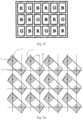
- the pattern region is set to the opening regions of the mask for manufacturing green sub-pixels, the opening width of the opening region is much larger than that of the FMM used in the conventional bar-shape arrangement. It should be understood that the criss-cross lateral and vertical lines disposed in Figs. 4A and 4B are for the ease of observing the location and the width of the opening regions corresponding to respective sub-pixels and are absent in the actual mask.
- the opening widths of the mask for red sub-pixels, blue sub-pixels or green sub-pixels are all increased, which thus is favorable for the design of FMM and the evaporation process for organic layer and makes it easier to implement high resolution. It can also be seen that, compared to the pixel structure of one pixel unit consisting of three sub-pixels in the prior art, the pixel structure in the present embodiment can simplify manufacture process largely, thus the FMM process can be implemented more easier.
- each pixel unit only consists of two sub-pixels, and each sub-pixel is connected to one data line receiving pixel information (the same as that in the related art). That is, the first sub-pixel 11 and the second sub-pixel 12 in the first pixel unit 1 are connected to two data lines (not shown in Figs. 2A and 2B ), respectively, and the third sub-pixel 21 and fourth sub-pixel 22 in the second pixel unit 2 are connected to two data lines respectively.
- the data lines in this embodiment are less than that in the related art, so that the power consumption of the display device is reduced and the aperture ratio of the display device is increased, which improves the brightness of the pixel structure in the display device accordingly.
- This embodiment provides a display method, according to the claimed invention, of the pixel structure in the first embodiment.
- one pixel unit consists of two sub-pixels and the pixel display with higher resolution may be implemented in conjunction with pixel-sharing algorithm.
- the first pixel unit 1 additionally uses at least one of the third sub-pixels 21 from adjacent second pixel units 2 to display
- the second pixel unit 2 additionally uses at least one of the first sub-pixels 11 from adjacent first pixel units 1 to display, so that both of the first pixel unit 1 and the second pixel unit 2 can display the pixel display information for sub-pixels of three basic colors.
- the first pixel unit 1 having a red sub-pixel and a green sub-pixel additionally uses the blue sub-pixel in an adjacent second pixel unit 2 to implement the display of three primary colors of RGB.
- the second pixel unit 2 having a blue sub-pixel and a green sub-pixel additionally uses the red sub-pixel in an adjacent first pixel unit 1 to implement the display of three primary colors of RGB.
- the detailed principle of additionally using is that, as shown in Fig.
- each pixel unit may additionally uses the sub-pixel of its missing color from its adjacent pixel unit on its either side, for example, additionally uses the sub-pixel from its adjacent pixel unit on its right side or left side, or additionally uses the sub-pixel from its adjacent pixel unit on its upper side or bottom side; and a plurality of sub-pixels may be additionally used, and only one sub-pixel may also be additionally used, both of which are not limited herein.
- a data source of pixel display information is provided first to input pixel data including RGB color information into each of the first pixel units 1 and the second pixel units 2, the display method of the pixel structure comprising the following steps: Step S1: obtaining the theoretical brightness values of colors corresponding to the basic colors of the first sub-pixel 11 and the second sub-pixel 12 in the first pixel unit 1 from the data source of pixel display information, and obtaining the theoretical brightness values of colors corresponding to the basic colors of the third sub-pixel 21 and the fourth sub-pixel 22 in the second pixel unit 2.
- the pixel data is color-separated, amplified and corrected to obtain three primary colors, and then is matrix-transformed to obtain a brightness signal, which is the theoretical brightness values of colors corresponding to three primary colors.
- the process of this part may use any processing method of brightness separation in the related art, thus not described in detail herein.
- Step S2 obtaining the actual brightness values of the first sub-pixel 11, the second sub-pixel 12, the third sub-pixel 21 and the fourth sub-pixel 22 by calculation.
- the actual brightness value of the first sub-pixel 11 in the first pixel unit 1 is obtained by weighting the theoretical brightness value of red color needed to be displayed in the pixel unit and the theoretical brightness value of red color needed to be displayed in at least one of the second pixel units 2 in its adjacent rows or columns.
- the calculation method of the actual brightness value of the third sub-pixel 21 in the second pixel unit 2 is similar.
- the actual brightness values of the second sub-pixel 12 and the fourth sub-pixel 22 are set to the theoretical brightness values of colors corresponding to their basic colors.
- the actual brightness value of the first sub-pixel 11 is set to a weighted sum of the theoretical brightness value of the basic color corresponding to the first sub-pixel 11 needed in the first pixel unit 1 and that of the basic color corresponding to the first sub-pixel 11 needed in at least one of its adjacent second pixel units 2.
- the actual brightness value of the third sub-pixel 21 is set to a weighted sum of the theoretical brightness value of the basic color corresponding to the third sub-pixel 21 needed in the second pixel unit 2 and that of the basic color corresponding to the third sub-pixel 21 needed in at least one of its adjacent first pixel units 1.
- the first pixel unit 1 additionally uses the third sub-pixels 21 in its N adjacent second pixel units 2 to display the sub-pixel of the basic color missing in the said first pixel unit 1
- the second pixel unit 2 additionally uses the first sub-pixels 11 in its N adjacent first pixel units 1 to display the sub-pixel of the basic color missing in the said second pixel unit 2, thereby implementing the display of three primary colors of RGB.
- both of the weighted values of the theoretical brightness values of the first sub-pixel 11 and the third sub pixel 21 are 1/N, wherein N ⁇ 1. It should be understood that the weighted value may be adjusted properly according to the overall picture effect of image corresponding to the pixel data to obtain appropriate weighted sums.
- the first pixel unit 1 additionally uses the third sub-pixel 21 in one adjacent second pixel unit 2 to display
- the second pixel unit 2 additionally uses the first sub-pixel 11 in one adjacent first pixel unit 1 to display.
- both of the weighted values of the theoretical brightness values of the first sub-pixel 11 and the third sub-pixel 21 are 1/2.
- the final actual brightness value of the actual sub-pixel is the sum of the products by multiplying the theoretical brightness value of the basic color of the actual sub-pixel in pixel unit, in which the actual sub-pixel is located, and the theoretical brightness values of the sub-pixels, additionally used by the actual sub-pixel, having the same basic color in its adjacent pixel units by their weighted values respectively.
- each pixel unit may additionally use the sub-pixel having its missing basic color in the adjacent pixel unit on its right side for example, since each red sub-pixel and each blue sub-pixel are used in the display of two pixel units, the input data signal of the sub-pixels are the weighted sum of two sub-pixel signals, for example, for a blue sub-pixel, its input signal is the sum of the signal of the blue sub-pixel in its own pixel unit and the signal of the blue sub-pixel needed for normal display in an adjacent second pixel unit 2, both of which may take the half portion respectively, for example.
- Step S3 inputting the actual brightness values into the first sub-pixel 11, the second sub-pixel 12, the third sub-pixel 21 and the fourth sub-pixel 22 to implement the display of three primary colors of RGB, thereby implementing the image display.
- the actual brightness values of the respective sub-pixels obtained in the step S2 are input into the first sub-pixel 11, the second sub-pixel 12, the third sub-pixel 21 and the fourth sub-pixel 22 to implement the image display.
- each sub-pixel is connected to one data line, and in this step, the actual brightness values of respective sub-pixels obtained in Step S2 are output through the data lines connected with the first sub-pixel 11, the second sub-pixel 12, the third sub-pixel 21 and the fourth sub-pixel 22 respectively.
- the theoretical brightness values corresponding to three basic colors in one pixel unit may be converted into the actual brightness values corresponding to two sub-pixels in one pixel unit by a process unit or data conversion module, and connected to one pixel unit through two data lines, and detailed process of data conversion is omitted herein.
- This display method of pixel structure implements the display of three primary colors for the pixel units having two sub-pixels by using the pixel units comprising only two sub-pixels and simple pixel-sharing algorithm.
- This embodiment not being part of the present invention, provides a display device which uses the pixel structure in the first embodiment and the display method of pixel structure in the second embodiment.
- the display device may be any product or component with the function of display, such as liquid crystal panels, electronic paper, OLED panels, mobile phones, tablet computers, televisions, displays, notebook computers, digital picture frames, navigators and the like.
- the display device shows high yield since the pixel structure thereof is significantly beneficial to the evaporation process for organic layer. Furthermore, the display device shows good display effect for the reason that the pixel structure thereof achieves higher brightness and color uniformity.
- the pixel structure and the display method thereof increases the aperture ratio by improving the pixel arrangement, and correspondingly increases the brightness of pixel structure and the pixel resolution; in the meantime, a display method with respect to the above pixel structure is designed, which is capable of implementing normal image display and preventing the error of color edge and the color nonuniformity due to the pixel arrangements in the related art, thereby improving the display effect of display devices and solving the problems that the resolution of display device, especially of organic light emitting display device, is hard to improve due to the process issue in the related art.
Landscapes
- Physics & Mathematics (AREA)
- Engineering & Computer Science (AREA)
- General Physics & Mathematics (AREA)
- Computer Hardware Design (AREA)
- Theoretical Computer Science (AREA)
- Nonlinear Science (AREA)
- Optics & Photonics (AREA)
- Crystallography & Structural Chemistry (AREA)
- Chemical & Material Sciences (AREA)
- Mathematical Physics (AREA)
- Microelectronics & Electronic Packaging (AREA)
- Electroluminescent Light Sources (AREA)
- Devices For Indicating Variable Information By Combining Individual Elements (AREA)
- Liquid Crystal (AREA)
- Control Of El Displays (AREA)
- Liquid Crystal Display Device Control (AREA)
- Control Of Indicators Other Than Cathode Ray Tubes (AREA)
Claims (10)
- Un procédé d'affichage d'une structure de pixels,dans lequel la structure de pixels comprend des premières unités de pixels (1) et des deuxièmes unités de pixels (2) qui sont agencées séquentiellement dans des positions décalées,dans lequel les premières unités de pixel et les deuxièmes unités de pixel sont agencées de manière alternée dans une direction des rangées et une direction des colonnes, et à la fois les premières unités de pixel dans deux rangées adjacentes et les deuxièmes unités de pixel dans deux rangées adjacentes sont agencées de façon à décaler une distance d'unité de pixel dans la direction des rangées, et à la fois les premières unités de pixels dans deux colonnes adjacentes et les deuxièmes unités de pixels dans deux colonnes adjacentes sont agencées de façon à décaler une distance d'unité de pixel dans la direction des colonnes ;dans lequel la première unité de pixel comprend un premier sous-pixel (11) et un deuxième sous-pixel (12) agencés sur une ligne oblique par rapport à la direction des rangées et à la direction des colonnes, et la deuxième unité de pixel comprend un troisième sous-pixel (21) et un quatrième sous-pixel (22) disposé en ligne oblique par rapport à la direction des rangées et à la direction des colonnes, le premier sous-pixel et le troisième sous-pixel ayant des couleurs de base différentes, et le deuxième sous-pixel et le quatrième sous-pixel ayant la même couleur de base ;dans lequel chacune des formes du premier sous-pixel, du deuxième sous-pixel, du troisième sous-pixel et du quatrième sous-pixel est un motif à symétrie axiale avec un axe de symétrie s'étendant dans une direction parallèle à la direction des rangées ou la direction des colonnes ;dans lequel le premier sous-pixel, le deuxième sous-pixel, le troisième sous-pixel et le quatrième sous-pixel ont tous une forme de losange ou une forme carrée, et une diagonale de chacun parmi le premier sous-pixel, le deuxième sous-pixel, le troisième sous-pixel et le quatrième sous-pixel est sélectionnée comme étant l'axe de symétrie du sous-pixel s'étendant dans une direction parallèle à la direction des rangées ou à la direction des colonnes, le long de laquelle le premier sous-pixel, le deuxième sous-pixel, le troisième sous-pixel et le quatrième sous-pixel sont agencés ;dans lequel la première unité de pixel utilise en outre au moins un des troisièmes sous-pixels de deuxièmes unités de pixel adjacentes pour l'affichage, et la deuxième unité de pixel utilise en outre au moins l'un des premiers sous-pixels de premières unités de pixel adjacentes pour l'affichage, de sorte que tant la première unité de pixel que la deuxième unité de pixel sont aptes à afficher les informations d'affichage de pixel pour des sous-pixels de trois couleurs de base,le procédé d'affichage comprenant :Étape S1 : à partir de la source de données d'informations d'affichage de pixels, obtention de valeurs de luminosité théoriques de couleurs correspondant aux couleurs de base du premier sous-pixel et du deuxième sous-pixel dans la première unité de pixels, et obtention de valeurs de luminosité théoriques de couleurs correspondant aux couleurs de base du troisième sous-pixel et du quatrième sous-pixel dans la deuxième unité de pixel ;Étape S2 : obtention des valeurs de luminosité réelles du premier sous-pixel, du deuxième sous-pixel, du troisième sous-pixel et du quatrième sous-pixel par calcul ; etÉtape S3 : entrée des valeurs de luminosité réelles dans le premier sous-pixel, le deuxième sous-pixel, le troisième sous-pixel et le quatrième sous-pixel pour mettre en oeuvre l'affichage d'image ;à l'étape S2, les valeurs de luminosité réelles du deuxième sous-pixel et du quatrième sous-pixel sont réglées sur les valeurs de luminosité théoriques des couleurs correspondant à leurs couleurs de base ;la valeur de luminosité réelle du premier sous-pixel est réglée sur une somme pondérée de la valeur de luminosité théorique de la couleur de base correspondant au premier sous-pixel nécessaire dans la première unité de pixel et de la valeur de luminosité théorique de la couleur de base correspondant au premier sous-pixel nécessaire dans au moins une de ses deuxièmes unités de pixel adjacentes ; etla valeur de luminosité réelle du troisième sous-pixel est fixée à une somme pondérée de la valeur de luminosité théorique de la couleur de base correspondant au troisième sous-pixel nécessaire dans la deuxième unité de pixel et de la valeur de luminosité théorique de la couleur de base correspondant au troisième sous-pixel nécessaire dans au moins une de ses premières unités de pixels adjacentes, etla première unité de pixel utilise en outre un troisième sous-pixel de sa deuxième unité de pixel adjacente pour l'affichage, et la deuxième unité de pixel utilise en outre un premier sous-pixel de sa première unité de pixel adjacente pour l'affichage ; de manière correspondante, à l'étape S2, les deux valeurs pondérées des valeurs de luminosité théoriques du premier sous-pixel et du troisième sous-pixel sont de 1/2.
- Le procédé d'affichage selon la revendication 1,
dans lequel les premiers sous-pixels et les deuxièmes sous-pixels dans les premières unités de pixels sont disposés dans deux rangées adjacentes et deux colonnes adjacentes de sous-pixels, et les troisièmes sous-pixels et les quatrièmes sous-pixels dans les deuxièmes unités de pixels sont disposés en deux rangées adjacentes et deux colonnes adjacentes de sous-pixels, de sorte que les premiers sous-pixels et les troisièmes sous-pixels sont agencés de manière alternée tour à tour dans la direction des rangées ou la direction des colonnes, respectivement, et les deuxièmes sous-pixels et les quatrièmes sous-pixels sont agencés de manière alternée tour à tour dans la direction des rangées ou dans la direction des colonnes, respectivement. - Le procédé d'affichage selon la revendication 2, dans lequel les premiers sous-pixels et les troisièmes sous-pixels sont disposés de manière alternée en lignes impaires et en colonnes impaires, et les deuxièmes sous-pixels et les quatrièmes sous-pixels sont disposés de manière alternée en lignes paires et en colonnes paires.
- Le procédé d'affichage selon la revendication 3, dans lequel les centres des premiers sous-pixels et des troisièmes sous-pixels situés dans la même rangée ou colonne sont dans la même ligne, et les centres des deuxièmes sous-pixels et des quatrièmes sous-pixels situés dans la même rangée ou colonne sont dans la même ligne ; et
dans lequel les premiers sous-pixels, les deuxièmes sous-pixels, les troisièmes sous-pixels et les quatrièmes sous-pixels sont agencés uniformément. - Le procédé d'affichage selon la revendication 4, dans lequel,dans une même colonne, le centre du premier sous-pixel est situé dans la bissectrice perpendiculaire d'une ligne reliant les centres de deux troisièmes sous-pixels adjacents au premier sous-pixel ;dans une même ligne, le centre du premier sous-pixel est situé dans la bissectrice perpendiculaire d'une ligne reliant les centres de deux troisièmes sous-pixels adjacents au premier sous-pixel ;dans une même colonne, le centre du troisième sous-pixel est situé dans la bissectrice perpendiculaire d'une ligne reliant les centres de deux premiers sous-pixels adjacents au troisième sous-pixel ; etdans une même rangée, le centre du troisième sous-pixel est situé dans la bissectrice perpendiculaire d'une ligne reliant les centres de deux premiers sous-pixels adjacents au troisième sous-pixel.
- Le procédé d'affichage selon la revendication 5, dans lequel le deuxième sous-pixel ou le quatrième sous-pixel est situé dans une direction d'un angle oblique de 45 degrés par rapport au premier sous-pixel ou au troisième sous-pixel.
- Le procédé d'affichage selon la revendication 6, dans lequel la surface du deuxième sous-pixel est la même que celle du quatrième sous-pixel, et la surface du premier sous-pixel est la même que celle du troisième sous-pixel et est plus grande que celle du deuxième sous-pixel ; ou
la surface du deuxième sous-pixel est la même que celle du quatrième sous-pixel, la surface du troisième sous-pixel est supérieure à celle du premier sous-pixel et la surface du premier sous-pixel est supérieure à celle du deuxième sous-pixel. - Le procédé d'affichage selon la revendication 7, dans lequel une distance entre le premier sous-pixel et le deuxième sous-pixel adjacents l'un à l'autre est égale à une distance entre le troisième sous-pixel et le quatrième sous-pixel adjacents l'un à l'autre, et une distance entre le premier sous-pixel et le troisième sous-pixel adjacents l'un à l'autre est inférieure à une distance entre le deuxième sous-pixel et le quatrième sous-pixel adjacents l'un à l'autre ; et
une distance entre deux sous-pixels adjacents est définie comme étant une longueur d'une ligne reliant deux points les plus proches des deux sous-pixels adjacents. - Le procédé d'affichage selon l'une quelconque des revendications 1 à 8, dans lequel les couleurs de base comprennent le rouge, le vert et le bleu, la couleur de base du premier sous-pixel est le rouge, la couleur de base du troisième sous-pixel est le bleu, et les couleurs de base des deuxième et quatrième sous-pixels sont le vert.
- Le procédé d'affichage selon l'une quelconque des revendications 1 à 8, dans lequel le premier sous-pixel et le deuxième sous-pixel dans la première unité de pixel sont respectivement connectés à deux lignes de données, et le troisième sous-pixel et le quatrième sous-pixel dans la deuxième unité de pixel sont connectés à deux lignes de données respectivement, les lignes de données étant utilisées pour recevoir les informations d'affichage de pixel.
Priority Applications (1)
| Application Number | Priority Date | Filing Date | Title |
|---|---|---|---|
| EP23165103.5A EP4220290A1 (fr) | 2014-09-30 | 2015-01-20 | Structure de pixel et son procédé d'affichage, et dispositif d'affichage |
Applications Claiming Priority (2)
| Application Number | Priority Date | Filing Date | Title |
|---|---|---|---|
| CN201410521724.0A CN104282727B (zh) | 2014-09-30 | 2014-09-30 | 一种像素结构及其显示方法、显示装置 |
| PCT/CN2015/071097 WO2016050018A1 (fr) | 2014-09-30 | 2015-01-20 | Structure de pixels et dispositif d'affichage de celle-ci, et appareil d'affichage |
Related Child Applications (2)
| Application Number | Title | Priority Date | Filing Date |
|---|---|---|---|
| EP23165103.5A Division EP4220290A1 (fr) | 2014-09-30 | 2015-01-20 | Structure de pixel et son procédé d'affichage, et dispositif d'affichage |
| EP23165103.5A Division-Into EP4220290A1 (fr) | 2014-09-30 | 2015-01-20 | Structure de pixel et son procédé d'affichage, et dispositif d'affichage |
Publications (3)
| Publication Number | Publication Date |
|---|---|
| EP3203523A1 EP3203523A1 (fr) | 2017-08-09 |
| EP3203523A4 EP3203523A4 (fr) | 2018-05-30 |
| EP3203523B1 true EP3203523B1 (fr) | 2023-05-10 |
Family
ID=52257443
Family Applications (2)
| Application Number | Title | Priority Date | Filing Date |
|---|---|---|---|
| EP15793668.3A Active EP3203523B1 (fr) | 2014-09-30 | 2015-01-20 | Méthode d'affichage pour une structure de pixel |
| EP23165103.5A Pending EP4220290A1 (fr) | 2014-09-30 | 2015-01-20 | Structure de pixel et son procédé d'affichage, et dispositif d'affichage |
Family Applications After (1)
| Application Number | Title | Priority Date | Filing Date |
|---|---|---|---|
| EP23165103.5A Pending EP4220290A1 (fr) | 2014-09-30 | 2015-01-20 | Structure de pixel et son procédé d'affichage, et dispositif d'affichage |
Country Status (6)
| Country | Link |
|---|---|
| US (1) | US9697760B2 (fr) |
| EP (2) | EP3203523B1 (fr) |
| JP (3) | JP2017533475A (fr) |
| KR (5) | KR20160056887A (fr) |
| CN (1) | CN104282727B (fr) |
| WO (1) | WO2016050018A1 (fr) |
Families Citing this family (86)
| Publication number | Priority date | Publication date | Assignee | Title |
|---|---|---|---|---|
| CN104282727B (zh) | 2014-09-30 | 2017-08-29 | 京东方科技集团股份有限公司 | 一种像素结构及其显示方法、显示装置 |
| CN104375302B (zh) * | 2014-10-27 | 2020-09-08 | 上海中航光电子有限公司 | 一种像素结构、显示面板及其像素补偿方法 |
| CN104362170B (zh) * | 2014-11-28 | 2017-04-12 | 京东方科技集团股份有限公司 | 一种有机电致发光显示器件、其驱动方法及相关装置 |
| JP6654280B2 (ja) * | 2015-01-14 | 2020-02-26 | 天馬微電子有限公司 | 画素アレイ及び電気光学装置並びに電気機器並びに画素アレイの駆動方法 |
| CN104617126B (zh) * | 2015-01-21 | 2017-06-30 | 信利(惠州)智能显示有限公司 | 一种有机发光二极管像素排列结构 |
| CN104597655B (zh) * | 2015-02-13 | 2017-06-27 | 京东方科技集团股份有限公司 | 一种像素排列结构、显示面板及显示装置 |
| US10134330B2 (en) | 2015-03-17 | 2018-11-20 | Kunshan Yunyinggu Electronic Technology Co., Ltd. | Subpixel arrangement for displays and driving circuit thereof |
| ES2795400T3 (es) | 2015-03-17 | 2020-11-23 | Kunshan Yunyinggu Electronic Tech Co Ltd | Disposición de subpíxeles para pantallas y circuito de excitación de la misma |
| CN104809956B (zh) * | 2015-04-24 | 2017-07-18 | 京东方科技集团股份有限公司 | 像素结构、显示基板和显示装置 |
| CN104992688B (zh) * | 2015-08-05 | 2018-01-09 | 京东方科技集团股份有限公司 | 像素阵列、显示装置及其驱动方法和驱动装置 |
| CN105047092B (zh) * | 2015-08-06 | 2018-07-06 | 上海和辉光电有限公司 | 显示器及其像素阵列 |
| CN105185229B (zh) * | 2015-08-28 | 2017-11-10 | 厦门天马微电子有限公司 | 显示装置及其显示方法 |
| CN106486514B (zh) * | 2015-08-31 | 2023-12-01 | 昆山国显光电有限公司 | 像素结构以及oled显示面板 |
| CN113192459A (zh) * | 2015-09-02 | 2021-07-30 | 天马微电子股份有限公司 | 显示装置 |
| KR102369368B1 (ko) * | 2015-09-30 | 2022-03-02 | 엘지디스플레이 주식회사 | 영상 처리 회로 및 그를 가지는 표시 장치 |
| WO2017055971A1 (fr) * | 2015-10-01 | 2017-04-06 | Semiconductor Energy Laboratory Co., Ltd. | Dispositif d'affichage et son procédé de fabrication |
| CN105445949B (zh) | 2016-01-26 | 2020-04-28 | 京东方科技集团股份有限公司 | 一种三维显示装置 |
| US10854684B2 (en) | 2016-02-18 | 2020-12-01 | Boe Technology Group Co., Ltd. | Pixel arrangement structure and driving method thereof, display substrate and display device |
| CN110133899A (zh) | 2018-02-09 | 2019-08-16 | 京东方科技集团股份有限公司 | 像素排列结构、显示基板、显示装置 |
| US11233096B2 (en) | 2016-02-18 | 2022-01-25 | Boe Technology Group Co., Ltd. | Pixel arrangement structure and driving method thereof, display substrate and display device |
| CN110137213B (zh) | 2018-02-09 | 2025-03-25 | 京东方科技集团股份有限公司 | 像素排列结构及其显示方法、显示基板 |
| CN110137215B (zh) * | 2018-02-09 | 2025-01-14 | 京东方科技集团股份有限公司 | 像素排列结构、显示基板和显示装置 |
| CN110134353B (zh) | 2018-02-09 | 2021-04-27 | 京东方科技集团股份有限公司 | 颜色补偿方法、补偿装置以及显示装置 |
| WO2021016946A1 (fr) | 2019-07-31 | 2021-02-04 | 京东方科技集团股份有限公司 | Substrat d'affichage et son procédé de préparation, panneau d'affichage et appareil d'affichage |
| US11747531B2 (en) | 2016-02-18 | 2023-09-05 | Chengdu Boe Optoelectronics Technology Co., Ltd. | Display substrate, fine metal mask set and manufacturing method thereof |
| US11448807B2 (en) | 2016-02-18 | 2022-09-20 | Chengdu Boe Optoelectronics Technology Co., Ltd. | Display substrate, fine metal mask set and manufacturing method thereof |
| US11264430B2 (en) | 2016-02-18 | 2022-03-01 | Chengdu Boe Optoelectronics Technology Co., Ltd. | Pixel arrangement structure with misaligned repeating units, display substrate, display apparatus and method of fabrication thereof |
| CN107275360B (zh) * | 2016-04-01 | 2020-10-16 | 乐金显示有限公司 | 有机发光显示装置 |
| CN107887404B (zh) * | 2016-09-29 | 2020-04-07 | 昆山国显光电有限公司 | Amoled像素结构及显示装置 |
| CN106652805B (zh) * | 2016-10-21 | 2019-03-19 | 上海天马微电子有限公司 | 显示面板和显示装置 |
| KR102578167B1 (ko) | 2016-11-02 | 2023-09-14 | 삼성디스플레이 주식회사 | 표시 장치의 구동 방법 및 이를 수행하는 표시 장치 |
| TWI614740B (zh) * | 2016-11-04 | 2018-02-11 | 創王光電股份有限公司 | 顯示裝置及用於掃描顯示裝置之子像素陣列之方法 |
| CN106530989A (zh) * | 2016-12-23 | 2017-03-22 | 上海天马有机发光显示技术有限公司 | 一种像素排列结构、显示面板及显示装置 |
| CN106783927B (zh) * | 2016-12-28 | 2020-02-11 | 上海天马有机发光显示技术有限公司 | 一种oled显示装置及其制作方法 |
| CN107248378B (zh) * | 2017-06-12 | 2019-07-23 | Oppo广东移动通信有限公司 | 像素阵列及显示器 |
| US20180357953A1 (en) * | 2017-06-12 | 2018-12-13 | Guangdong Oppo Mobile Telecommunications Corp., Ltd. | Pixel array and display having the same and electronic device |
| WO2019026132A1 (fr) * | 2017-07-31 | 2019-02-07 | シャープ株式会社 | Dispositif d'affichage |
| CN109426038A (zh) * | 2017-08-25 | 2019-03-05 | 合肥捷达微电子有限公司 | 显示面板及显示装置 |
| CN107808405A (zh) * | 2017-09-14 | 2018-03-16 | 遵义师范学院 | 一种像素结构转换方法 |
| CN107577078B (zh) * | 2017-09-19 | 2021-11-12 | 厦门天马微电子有限公司 | 一种显示面板及显示装置 |
| CN109841747B (zh) * | 2017-11-27 | 2021-09-24 | 上海和辉光电股份有限公司 | 一种有机发光显示面板及显示装置 |
| CN109994504A (zh) * | 2018-01-02 | 2019-07-09 | 京东方科技集团股份有限公司 | 一种像素排布结构及相关装置 |
| CN110137210B (zh) * | 2018-02-09 | 2025-06-27 | 京东方科技集团股份有限公司 | 一种像素排布结构及相关装置 |
| CN109994508B (zh) | 2018-01-02 | 2024-09-03 | 京东方科技集团股份有限公司 | 一种像素排布结构及相关装置 |
| US10991768B2 (en) | 2018-01-02 | 2021-04-27 | Boe Technology Group Co., Ltd. | Pixel arrangement, manufacturing method thereof, display panel, display device, and mask |
| US10909901B2 (en) | 2018-01-02 | 2021-02-02 | Boe Technology Group Co., Ltd. | Pixel arrangement, manufacturing method thereof, display panel, display device and mask |
| CN109994505B (zh) | 2018-01-02 | 2025-04-15 | 京东方科技集团股份有限公司 | 一种像素排布结构及相关装置 |
| CN109994507B (zh) * | 2018-01-02 | 2020-08-04 | 京东方科技集团股份有限公司 | 一种像素排布结构及相关装置 |
| CN108565277B (zh) | 2018-01-04 | 2021-09-28 | 上海天马有机发光显示技术有限公司 | 显示面板及其制作方法 |
| CN108154848B (zh) * | 2018-01-19 | 2020-11-17 | 昆山国显光电有限公司 | 像素排列的显示方法、装置及显示设备 |
| CN108364983A (zh) * | 2018-02-01 | 2018-08-03 | 武汉华星光电半导体显示技术有限公司 | 像素排列结构 |
| US11355556B2 (en) | 2018-02-01 | 2022-06-07 | Wuhan China Star Optoelectronics Semiconductor Display Technology Co., Ltd. | Display panel |
| CN110137208A (zh) * | 2018-02-09 | 2019-08-16 | 京东方科技集团股份有限公司 | 一种像素排布结构、高精度金属掩模板及显示装置 |
| CN114994973B (zh) * | 2018-02-09 | 2023-04-28 | 京东方科技集团股份有限公司 | 显示基板和显示装置 |
| CN110137211A (zh) * | 2018-02-09 | 2019-08-16 | 京东方科技集团股份有限公司 | 一种像素排布结构、高精度金属掩模板及显示装置 |
| US11574960B2 (en) | 2018-02-09 | 2023-02-07 | Boe Technology Group Co., Ltd. | Pixel arrangement structure, display substrate, display device and mask plate group |
| CN110137206B (zh) * | 2018-02-09 | 2025-01-21 | 京东方科技集团股份有限公司 | 一种像素排布结构及相关装置 |
| CN108300963B (zh) * | 2018-03-30 | 2019-08-27 | 昆山国显光电有限公司 | 一种掩模板 |
| CN110349528B (zh) * | 2018-04-03 | 2021-04-13 | 京东方科技集团股份有限公司 | 像素阵列及其驱动方法、显示装置 |
| CN108761391B (zh) * | 2018-05-29 | 2022-04-01 | 南京信息工程大学 | 一种模型类无设备目标定位方法 |
| CN108807475B (zh) * | 2018-05-31 | 2020-09-25 | 昆山国显光电有限公司 | 像素排布结构及oled显示面板 |
| CN110660823A (zh) * | 2018-06-29 | 2020-01-07 | 京东方科技集团股份有限公司 | 显示基板、其显示方法、显示装置及高精度金属掩模板 |
| CN110620129B (zh) | 2018-06-20 | 2022-02-01 | 京东方科技集团股份有限公司 | 显示基板、其驱动方法、显示装置及高精度金属掩模板 |
| CN110619813B (zh) | 2018-06-20 | 2021-05-14 | 京东方科技集团股份有限公司 | 显示基板、其驱动方法、显示装置及高精度金属掩模版 |
| WO2019242510A1 (fr) | 2018-06-20 | 2019-12-26 | 京东方科技集团股份有限公司 | Substrat d'affichage et son procédé de commande, et dispositif d'affichage |
| JP2020008662A (ja) * | 2018-07-05 | 2020-01-16 | 株式会社ジャパンディスプレイ | 表示装置 |
| CN108803180B (zh) * | 2018-08-09 | 2021-09-28 | 上海天马微电子有限公司 | 液晶面板和显示装置 |
| CN211743156U (zh) * | 2018-11-06 | 2020-10-23 | 京东方科技集团股份有限公司 | 像素排布结构、显示基板及显示装置 |
| CN109713027B (zh) * | 2019-02-28 | 2020-12-11 | 上海天马有机发光显示技术有限公司 | 一种有机发光显示面板的像素排布及有机发光显示面板 |
| KR102866754B1 (ko) | 2019-03-04 | 2025-09-30 | 삼성디스플레이 주식회사 | 표시 장치, 표시 장치의 제조장치 및 표시 장치의 제조방법 |
| KR102922035B1 (ko) * | 2019-05-16 | 2026-02-03 | 삼성디스플레이 주식회사 | 유기발광표시장치 |
| CN112673476B (zh) | 2019-07-31 | 2025-12-30 | 京东方科技集团股份有限公司 | 显示基板和显示装置 |
| CN110767733B (zh) * | 2019-10-31 | 2022-05-31 | 武汉天马微电子有限公司 | 一种显示面板和显示装置 |
| US12419175B2 (en) | 2019-12-10 | 2025-09-16 | Samsung Display Co., Ltd. | Display device, mask assembly, and apparatus for manufacturing display device |
| CN113035848B (zh) * | 2019-12-25 | 2025-01-14 | 深圳市聚飞光电股份有限公司 | 一种led灯板和显示装置 |
| KR102696841B1 (ko) * | 2019-12-31 | 2024-08-19 | 엘지디스플레이 주식회사 | 펜타일 형상의 발광 영역들을 포함하는 디스플레이 장치 |
| JP2021189336A (ja) * | 2020-06-01 | 2021-12-13 | 株式会社ジャパンディスプレイ | 表示装置 |
| CN114420722B (zh) | 2020-09-10 | 2026-03-06 | 京东方科技集团股份有限公司 | 显示基板及显示装置 |
| US12302730B2 (en) | 2020-09-29 | 2025-05-13 | Chengdu Boe Optoelectronics Technology Co., Ltd. | Pixel array and display device |
| MX2021016051A (es) | 2020-09-10 | 2022-04-07 | Boe Technology Group Co Ltd | Serie de pixeles y dispositivo de pantalla. |
| CN112419917A (zh) * | 2020-12-03 | 2021-02-26 | 夏林嘉 | 三基色全彩led显示屏的共享像素排列结构及共享方法 |
| KR20220121968A (ko) | 2021-02-25 | 2022-09-02 | 삼성디스플레이 주식회사 | 표시 장치 |
| CN114743465B (zh) * | 2022-02-28 | 2023-08-15 | 长春希达电子技术有限公司 | 一种发光像素排布结构、显示面板及电子设备 |
| CN114613309B (zh) * | 2022-03-25 | 2024-08-23 | 厦门天马显示科技有限公司 | 像素排列结构及显示面板和显示装置 |
| CN117133201B (zh) * | 2023-10-19 | 2024-02-02 | 长春希达电子技术有限公司 | 一种排布结构、虚拟像素复用方式及其控制方法 |
| CN117939957B (zh) * | 2024-03-25 | 2024-11-22 | 深圳市华星光电半导体显示技术有限公司 | 像素排列结构及显示装置 |
Citations (1)
| Publication number | Priority date | Publication date | Assignee | Title |
|---|---|---|---|---|
| US20140252321A1 (en) * | 2013-03-11 | 2014-09-11 | Samsung Display Co., Ltd. | Organic light-emitting display device |
Family Cites Families (24)
| Publication number | Priority date | Publication date | Assignee | Title |
|---|---|---|---|---|
| JPH08335060A (ja) * | 1996-06-28 | 1996-12-17 | Mitsubishi Electric Corp | マトリクス型カラー液晶表示装置の駆動方法 |
| CN1295945C (zh) * | 2000-12-20 | 2007-01-17 | 皇家菲利浦电子有限公司 | 场致发光彩色显示屏 |
| JP4299672B2 (ja) * | 2002-01-07 | 2009-07-22 | サムスン エレクトロニクス カンパニー リミテッド | 変調伝達関数を向上させたサブピクセル描画用のカラー平板表示サブピクセル構成およびレイアウト |
| JP2005062220A (ja) * | 2003-08-08 | 2005-03-10 | Sharp Corp | 表示パネルおよび表示装置 |
| JP2006292858A (ja) * | 2005-04-07 | 2006-10-26 | Matsushita Electric Ind Co Ltd | Led表示装置及び表示基板 |
| JP4781351B2 (ja) * | 2005-04-22 | 2011-09-28 | シャープ株式会社 | 表示装置 |
| KR100579048B1 (ko) * | 2005-09-27 | 2006-05-12 | 주식회사 한국싸인 | 전광판의 픽셀 형성 방법 |
| US7969428B2 (en) * | 2006-05-08 | 2011-06-28 | Global Oled Technology Llc | Color display system with improved apparent resolution |
| JP5481323B2 (ja) | 2010-09-01 | 2014-04-23 | 株式会社ジャパンディスプレイ | 画像表示装置の駆動方法 |
| TWI433104B (zh) * | 2011-06-30 | 2014-04-01 | Hannstar Display Corp | 雙閘線單元面板之測試線路及雙閘線單元面板之色彩顯示方法 |
| JP2013058323A (ja) * | 2011-09-07 | 2013-03-28 | Sony Corp | 発光パネル、表示装置および電子機器 |
| TWI484817B (zh) | 2011-12-15 | 2015-05-11 | Au Optronics Corp | 顯示面板 |
| KR101615332B1 (ko) * | 2012-03-06 | 2016-04-26 | 삼성디스플레이 주식회사 | 유기 발광 표시 장치의 화소 배열 구조 |
| KR102063973B1 (ko) * | 2012-09-12 | 2020-01-09 | 삼성디스플레이 주식회사 | 유기전계발광 표시장치 및 그의 구동방법 |
| EP3780113B1 (fr) * | 2012-09-13 | 2025-07-16 | Samsung Display Co., Ltd. | Structure de disposition de pixels pour dispositif d'affichage à diodes électroluminescentes organiques |
| KR101996432B1 (ko) * | 2012-09-19 | 2019-07-05 | 삼성디스플레이 주식회사 | 표시 장치 및 그 구동 방법 |
| CN103745684B (zh) * | 2013-11-13 | 2016-09-28 | 上海和辉光电有限公司 | 像素阵列、呈现图像于显示器上的方法及显示器 |
| CN103680325A (zh) * | 2013-12-17 | 2014-03-26 | 京东方科技集团股份有限公司 | 显示基板、显示面板和立体显示装置 |
| CN103714751B (zh) * | 2013-12-30 | 2016-06-22 | 北京京东方光电科技有限公司 | 像素阵列及其驱动方法、显示面板和显示装置 |
| CN103778882B (zh) * | 2014-01-26 | 2016-03-23 | 北京京东方光电科技有限公司 | 像素阵列及其驱动方法、显示面板和显示装置 |
| TWI515710B (zh) * | 2014-02-17 | 2016-01-01 | 友達光電股份有限公司 | 顯示器的驅動方法 |
| CN103943656B (zh) * | 2014-03-25 | 2017-01-18 | 京东方科技集团股份有限公司 | 有机发光二极管显示像素、显示面板及显示装置 |
| CN104282727B (zh) * | 2014-09-30 | 2017-08-29 | 京东方科技集团股份有限公司 | 一种像素结构及其显示方法、显示装置 |
| CN204102903U (zh) * | 2014-09-30 | 2015-01-14 | 京东方科技集团股份有限公司 | 一种像素结构及其显示装置 |
-
2014
- 2014-09-30 CN CN201410521724.0A patent/CN104282727B/zh active Active
-
2015
- 2015-01-20 EP EP15793668.3A patent/EP3203523B1/fr active Active
- 2015-01-20 KR KR1020167006415A patent/KR20160056887A/ko not_active Ceased
- 2015-01-20 KR KR1020187023774A patent/KR20180095735A/ko not_active Ceased
- 2015-01-20 WO PCT/CN2015/071097 patent/WO2016050018A1/fr not_active Ceased
- 2015-01-20 KR KR1020207023654A patent/KR102249871B1/ko active Active
- 2015-01-20 US US14/769,610 patent/US9697760B2/en active Active
- 2015-01-20 EP EP23165103.5A patent/EP4220290A1/fr active Pending
- 2015-01-20 KR KR1020207003501A patent/KR102146961B1/ko active Active
- 2015-01-20 JP JP2017536995A patent/JP2017533475A/ja active Pending
- 2015-01-20 KR KR1020197025737A patent/KR102076304B1/ko active Active
-
2019
- 2019-03-05 JP JP2019039640A patent/JP6759396B2/ja active Active
-
2020
- 2020-09-02 JP JP2020147610A patent/JP2020197752A/ja active Pending
Patent Citations (1)
| Publication number | Priority date | Publication date | Assignee | Title |
|---|---|---|---|---|
| US20140252321A1 (en) * | 2013-03-11 | 2014-09-11 | Samsung Display Co., Ltd. | Organic light-emitting display device |
Also Published As
| Publication number | Publication date |
|---|---|
| KR102249871B1 (ko) | 2021-05-11 |
| KR20180095735A (ko) | 2018-08-27 |
| KR20160056887A (ko) | 2016-05-20 |
| EP4220290A1 (fr) | 2023-08-02 |
| WO2016050018A1 (fr) | 2016-04-07 |
| CN104282727B (zh) | 2017-08-29 |
| US9697760B2 (en) | 2017-07-04 |
| JP2017533475A (ja) | 2017-11-09 |
| US20160253943A1 (en) | 2016-09-01 |
| KR20190104460A (ko) | 2019-09-09 |
| KR102146961B1 (ko) | 2020-08-24 |
| JP2020197752A (ja) | 2020-12-10 |
| JP6759396B2 (ja) | 2020-09-23 |
| KR20200016400A (ko) | 2020-02-14 |
| KR102076304B1 (ko) | 2020-02-11 |
| JP2019109541A (ja) | 2019-07-04 |
| EP3203523A1 (fr) | 2017-08-09 |
| KR20200099625A (ko) | 2020-08-24 |
| EP3203523A4 (fr) | 2018-05-30 |
| CN104282727A (zh) | 2015-01-14 |
Similar Documents
| Publication | Publication Date | Title |
|---|---|---|
| EP3203523B1 (fr) | Méthode d'affichage pour une structure de pixel | |
| JP6657127B2 (ja) | 画素構造、その表示方法、及び表示装置 | |
| US11568794B2 (en) | Pixel arrangement structure, metal mask, and display device | |
| US11380236B2 (en) | Sub-pixel arrangement structure, mask device, and display device | |
| KR101878087B1 (ko) | 픽셀 구조체 및 그 디스플레이 방법, 및 관련된 디스플레이 장치 | |
| US10074301B2 (en) | Display panel and driving method thereof, and display device | |
| CN204102903U (zh) | 一种像素结构及其显示装置 | |
| WO2019148678A1 (fr) | Structure d'agencement de pixel pour diode électroluminescente organique, et panneau d'affichage |
Legal Events
| Date | Code | Title | Description |
|---|---|---|---|
| PUAI | Public reference made under article 153(3) epc to a published international application that has entered the european phase |
Free format text: ORIGINAL CODE: 0009012 |
|
| STAA | Information on the status of an ep patent application or granted ep patent |
Free format text: STATUS: REQUEST FOR EXAMINATION WAS MADE |
|
| 17P | Request for examination filed |
Effective date: 20151120 |
|
| AK | Designated contracting states |
Kind code of ref document: A1 Designated state(s): AL AT BE BG CH CY CZ DE DK EE ES FI FR GB GR HR HU IE IS IT LI LT LU LV MC MK MT NL NO PL PT RO RS SE SI SK SM TR |
|
| AX | Request for extension of the european patent |
Extension state: BA ME |
|
| DAX | Request for extension of the european patent (deleted) | ||
| A4 | Supplementary search report drawn up and despatched |
Effective date: 20180504 |
|
| RIC1 | Information provided on ipc code assigned before grant |
Ipc: G02F 1/1362 20060101ALI20180426BHEP Ipc: H01L 27/32 20060101AFI20180426BHEP Ipc: G09G 3/20 20060101ALI20180426BHEP Ipc: G09G 3/3208 20160101ALI20180426BHEP |
|
| STAA | Information on the status of an ep patent application or granted ep patent |
Free format text: STATUS: EXAMINATION IS IN PROGRESS |
|
| 17Q | First examination report despatched |
Effective date: 20200709 |
|
| GRAP | Despatch of communication of intention to grant a patent |
Free format text: ORIGINAL CODE: EPIDOSNIGR1 |
|
| STAA | Information on the status of an ep patent application or granted ep patent |
Free format text: STATUS: GRANT OF PATENT IS INTENDED |
|
| INTG | Intention to grant announced |
Effective date: 20221216 |
|
| GRAS | Grant fee paid |
Free format text: ORIGINAL CODE: EPIDOSNIGR3 |
|
| GRAA | (expected) grant |
Free format text: ORIGINAL CODE: 0009210 |
|
| STAA | Information on the status of an ep patent application or granted ep patent |
Free format text: STATUS: THE PATENT HAS BEEN GRANTED |
|
| AK | Designated contracting states |
Kind code of ref document: B1 Designated state(s): AL AT BE BG CH CY CZ DE DK EE ES FI FR GB GR HR HU IE IS IT LI LT LU LV MC MK MT NL NO PL PT RO RS SE SI SK SM TR |
|
| REG | Reference to a national code |
Ref country code: GB Ref legal event code: FG4D |
|
| REG | Reference to a national code |
Ref country code: AT Ref legal event code: REF Ref document number: 1567583 Country of ref document: AT Kind code of ref document: T Effective date: 20230515 Ref country code: CH Ref legal event code: EP |
|
| REG | Reference to a national code |
Ref country code: DE Ref legal event code: R096 Ref document number: 602015083534 Country of ref document: DE |
|
| REG | Reference to a national code |
Ref country code: IE Ref legal event code: FG4D |
|
| P01 | Opt-out of the competence of the unified patent court (upc) registered |
Effective date: 20230527 |
|
| REG | Reference to a national code |
Ref country code: LT Ref legal event code: MG9D |
|
| REG | Reference to a national code |
Ref country code: NL Ref legal event code: MP Effective date: 20230510 |
|
| REG | Reference to a national code |
Ref country code: AT Ref legal event code: MK05 Ref document number: 1567583 Country of ref document: AT Kind code of ref document: T Effective date: 20230510 |
|
| PG25 | Lapsed in a contracting state [announced via postgrant information from national office to epo] |
Ref country code: SE Free format text: LAPSE BECAUSE OF FAILURE TO SUBMIT A TRANSLATION OF THE DESCRIPTION OR TO PAY THE FEE WITHIN THE PRESCRIBED TIME-LIMIT Effective date: 20230510 Ref country code: PT Free format text: LAPSE BECAUSE OF FAILURE TO SUBMIT A TRANSLATION OF THE DESCRIPTION OR TO PAY THE FEE WITHIN THE PRESCRIBED TIME-LIMIT Effective date: 20230911 Ref country code: NO Free format text: LAPSE BECAUSE OF FAILURE TO SUBMIT A TRANSLATION OF THE DESCRIPTION OR TO PAY THE FEE WITHIN THE PRESCRIBED TIME-LIMIT Effective date: 20230810 Ref country code: NL Free format text: LAPSE BECAUSE OF FAILURE TO SUBMIT A TRANSLATION OF THE DESCRIPTION OR TO PAY THE FEE WITHIN THE PRESCRIBED TIME-LIMIT Effective date: 20230510 Ref country code: ES Free format text: LAPSE BECAUSE OF FAILURE TO SUBMIT A TRANSLATION OF THE DESCRIPTION OR TO PAY THE FEE WITHIN THE PRESCRIBED TIME-LIMIT Effective date: 20230510 Ref country code: AT Free format text: LAPSE BECAUSE OF FAILURE TO SUBMIT A TRANSLATION OF THE DESCRIPTION OR TO PAY THE FEE WITHIN THE PRESCRIBED TIME-LIMIT Effective date: 20230510 |
|
| PG25 | Lapsed in a contracting state [announced via postgrant information from national office to epo] |
Ref country code: RS Free format text: LAPSE BECAUSE OF FAILURE TO SUBMIT A TRANSLATION OF THE DESCRIPTION OR TO PAY THE FEE WITHIN THE PRESCRIBED TIME-LIMIT Effective date: 20230510 Ref country code: PL Free format text: LAPSE BECAUSE OF FAILURE TO SUBMIT A TRANSLATION OF THE DESCRIPTION OR TO PAY THE FEE WITHIN THE PRESCRIBED TIME-LIMIT Effective date: 20230510 Ref country code: LV Free format text: LAPSE BECAUSE OF FAILURE TO SUBMIT A TRANSLATION OF THE DESCRIPTION OR TO PAY THE FEE WITHIN THE PRESCRIBED TIME-LIMIT Effective date: 20230510 Ref country code: LT Free format text: LAPSE BECAUSE OF FAILURE TO SUBMIT A TRANSLATION OF THE DESCRIPTION OR TO PAY THE FEE WITHIN THE PRESCRIBED TIME-LIMIT Effective date: 20230510 Ref country code: IS Free format text: LAPSE BECAUSE OF FAILURE TO SUBMIT A TRANSLATION OF THE DESCRIPTION OR TO PAY THE FEE WITHIN THE PRESCRIBED TIME-LIMIT Effective date: 20230910 Ref country code: HR Free format text: LAPSE BECAUSE OF FAILURE TO SUBMIT A TRANSLATION OF THE DESCRIPTION OR TO PAY THE FEE WITHIN THE PRESCRIBED TIME-LIMIT Effective date: 20230510 Ref country code: GR Free format text: LAPSE BECAUSE OF FAILURE TO SUBMIT A TRANSLATION OF THE DESCRIPTION OR TO PAY THE FEE WITHIN THE PRESCRIBED TIME-LIMIT Effective date: 20230811 |
|
| PG25 | Lapsed in a contracting state [announced via postgrant information from national office to epo] |
Ref country code: FI Free format text: LAPSE BECAUSE OF FAILURE TO SUBMIT A TRANSLATION OF THE DESCRIPTION OR TO PAY THE FEE WITHIN THE PRESCRIBED TIME-LIMIT Effective date: 20230510 |
|
| PG25 | Lapsed in a contracting state [announced via postgrant information from national office to epo] |
Ref country code: SK Free format text: LAPSE BECAUSE OF FAILURE TO SUBMIT A TRANSLATION OF THE DESCRIPTION OR TO PAY THE FEE WITHIN THE PRESCRIBED TIME-LIMIT Effective date: 20230510 |
|
| PG25 | Lapsed in a contracting state [announced via postgrant information from national office to epo] |
Ref country code: SM Free format text: LAPSE BECAUSE OF FAILURE TO SUBMIT A TRANSLATION OF THE DESCRIPTION OR TO PAY THE FEE WITHIN THE PRESCRIBED TIME-LIMIT Effective date: 20230510 Ref country code: SK Free format text: LAPSE BECAUSE OF FAILURE TO SUBMIT A TRANSLATION OF THE DESCRIPTION OR TO PAY THE FEE WITHIN THE PRESCRIBED TIME-LIMIT Effective date: 20230510 Ref country code: RO Free format text: LAPSE BECAUSE OF FAILURE TO SUBMIT A TRANSLATION OF THE DESCRIPTION OR TO PAY THE FEE WITHIN THE PRESCRIBED TIME-LIMIT Effective date: 20230510 Ref country code: EE Free format text: LAPSE BECAUSE OF FAILURE TO SUBMIT A TRANSLATION OF THE DESCRIPTION OR TO PAY THE FEE WITHIN THE PRESCRIBED TIME-LIMIT Effective date: 20230510 Ref country code: DK Free format text: LAPSE BECAUSE OF FAILURE TO SUBMIT A TRANSLATION OF THE DESCRIPTION OR TO PAY THE FEE WITHIN THE PRESCRIBED TIME-LIMIT Effective date: 20230510 Ref country code: CZ Free format text: LAPSE BECAUSE OF FAILURE TO SUBMIT A TRANSLATION OF THE DESCRIPTION OR TO PAY THE FEE WITHIN THE PRESCRIBED TIME-LIMIT Effective date: 20230510 |
|
| REG | Reference to a national code |
Ref country code: DE Ref legal event code: R097 Ref document number: 602015083534 Country of ref document: DE |
|
| PLBE | No opposition filed within time limit |
Free format text: ORIGINAL CODE: 0009261 |
|
| STAA | Information on the status of an ep patent application or granted ep patent |
Free format text: STATUS: NO OPPOSITION FILED WITHIN TIME LIMIT |
|
| 26N | No opposition filed |
Effective date: 20240213 |
|
| PG25 | Lapsed in a contracting state [announced via postgrant information from national office to epo] |
Ref country code: SI Free format text: LAPSE BECAUSE OF FAILURE TO SUBMIT A TRANSLATION OF THE DESCRIPTION OR TO PAY THE FEE WITHIN THE PRESCRIBED TIME-LIMIT Effective date: 20230510 |
|
| PG25 | Lapsed in a contracting state [announced via postgrant information from national office to epo] |
Ref country code: SI Free format text: LAPSE BECAUSE OF FAILURE TO SUBMIT A TRANSLATION OF THE DESCRIPTION OR TO PAY THE FEE WITHIN THE PRESCRIBED TIME-LIMIT Effective date: 20230510 Ref country code: IT Free format text: LAPSE BECAUSE OF FAILURE TO SUBMIT A TRANSLATION OF THE DESCRIPTION OR TO PAY THE FEE WITHIN THE PRESCRIBED TIME-LIMIT Effective date: 20230510 |
|
| PG25 | Lapsed in a contracting state [announced via postgrant information from national office to epo] |
Ref country code: MC Free format text: LAPSE BECAUSE OF FAILURE TO SUBMIT A TRANSLATION OF THE DESCRIPTION OR TO PAY THE FEE WITHIN THE PRESCRIBED TIME-LIMIT Effective date: 20230510 |
|
| PG25 | Lapsed in a contracting state [announced via postgrant information from national office to epo] |
Ref country code: MC Free format text: LAPSE BECAUSE OF FAILURE TO SUBMIT A TRANSLATION OF THE DESCRIPTION OR TO PAY THE FEE WITHIN THE PRESCRIBED TIME-LIMIT Effective date: 20230510 |
|
| REG | Reference to a national code |
Ref country code: CH Ref legal event code: PL |
|
| PG25 | Lapsed in a contracting state [announced via postgrant information from national office to epo] |
Ref country code: LU Free format text: LAPSE BECAUSE OF NON-PAYMENT OF DUE FEES Effective date: 20240120 |
|
| PG25 | Lapsed in a contracting state [announced via postgrant information from national office to epo] |
Ref country code: LU Free format text: LAPSE BECAUSE OF NON-PAYMENT OF DUE FEES Effective date: 20240120 |
|
| PG25 | Lapsed in a contracting state [announced via postgrant information from national office to epo] |
Ref country code: BE Free format text: LAPSE BECAUSE OF NON-PAYMENT OF DUE FEES Effective date: 20240131 |
|
| PG25 | Lapsed in a contracting state [announced via postgrant information from national office to epo] |
Ref country code: FR Free format text: LAPSE BECAUSE OF NON-PAYMENT OF DUE FEES Effective date: 20240131 |
|
| PG25 | Lapsed in a contracting state [announced via postgrant information from national office to epo] |
Ref country code: CH Free format text: LAPSE BECAUSE OF NON-PAYMENT OF DUE FEES Effective date: 20240131 |
|
| PG25 | Lapsed in a contracting state [announced via postgrant information from national office to epo] |
Ref country code: FR Free format text: LAPSE BECAUSE OF NON-PAYMENT OF DUE FEES Effective date: 20240131 Ref country code: CH Free format text: LAPSE BECAUSE OF NON-PAYMENT OF DUE FEES Effective date: 20240131 Ref country code: BE Free format text: LAPSE BECAUSE OF NON-PAYMENT OF DUE FEES Effective date: 20240131 |
|
| REG | Reference to a national code |
Ref country code: BE Ref legal event code: MM Effective date: 20240131 |
|
| PG25 | Lapsed in a contracting state [announced via postgrant information from national office to epo] |
Ref country code: BG Free format text: LAPSE BECAUSE OF FAILURE TO SUBMIT A TRANSLATION OF THE DESCRIPTION OR TO PAY THE FEE WITHIN THE PRESCRIBED TIME-LIMIT Effective date: 20230510 |
|
| PG25 | Lapsed in a contracting state [announced via postgrant information from national office to epo] |
Ref country code: BG Free format text: LAPSE BECAUSE OF FAILURE TO SUBMIT A TRANSLATION OF THE DESCRIPTION OR TO PAY THE FEE WITHIN THE PRESCRIBED TIME-LIMIT Effective date: 20230510 |
|
| PG25 | Lapsed in a contracting state [announced via postgrant information from national office to epo] |
Ref country code: IE Free format text: LAPSE BECAUSE OF NON-PAYMENT OF DUE FEES Effective date: 20240120 |
|
| PG25 | Lapsed in a contracting state [announced via postgrant information from national office to epo] |
Ref country code: IE Free format text: LAPSE BECAUSE OF NON-PAYMENT OF DUE FEES Effective date: 20240120 |
|
| PG25 | Lapsed in a contracting state [announced via postgrant information from national office to epo] |
Ref country code: CY Free format text: LAPSE BECAUSE OF FAILURE TO SUBMIT A TRANSLATION OF THE DESCRIPTION OR TO PAY THE FEE WITHIN THE PRESCRIBED TIME-LIMIT; INVALID AB INITIO Effective date: 20150120 |
|
| PG25 | Lapsed in a contracting state [announced via postgrant information from national office to epo] |
Ref country code: HU Free format text: LAPSE BECAUSE OF FAILURE TO SUBMIT A TRANSLATION OF THE DESCRIPTION OR TO PAY THE FEE WITHIN THE PRESCRIBED TIME-LIMIT; INVALID AB INITIO Effective date: 20150120 |
|
| PG25 | Lapsed in a contracting state [announced via postgrant information from national office to epo] |
Ref country code: TR Free format text: LAPSE BECAUSE OF FAILURE TO SUBMIT A TRANSLATION OF THE DESCRIPTION OR TO PAY THE FEE WITHIN THE PRESCRIBED TIME-LIMIT Effective date: 20230510 |
|
| PGFP | Annual fee paid to national office [announced via postgrant information from national office to epo] |
Ref country code: GB Payment date: 20260123 Year of fee payment: 12 |
|
| PGFP | Annual fee paid to national office [announced via postgrant information from national office to epo] |
Ref country code: DE Payment date: 20260121 Year of fee payment: 12 |