EP3203734A2 - Étalonnage de caméra - Google Patents
Étalonnage de caméra Download PDFInfo
- Publication number
- EP3203734A2 EP3203734A2 EP17154862.1A EP17154862A EP3203734A2 EP 3203734 A2 EP3203734 A2 EP 3203734A2 EP 17154862 A EP17154862 A EP 17154862A EP 3203734 A2 EP3203734 A2 EP 3203734A2
- Authority
- EP
- European Patent Office
- Prior art keywords
- camera
- pulse
- light
- output
- width
- Prior art date
- Legal status (The legal status is an assumption and is not a legal conclusion. Google has not performed a legal analysis and makes no representation as to the accuracy of the status listed.)
- Withdrawn
Links
- 238000012360 testing method Methods 0.000 claims abstract description 15
- 238000005259 measurement Methods 0.000 claims abstract description 13
- 238000000034 method Methods 0.000 claims description 18
- 238000012546 transfer Methods 0.000 claims description 5
- 230000010354 integration Effects 0.000 claims description 2
- 230000006870 function Effects 0.000 description 6
- 238000004519 manufacturing process Methods 0.000 description 5
- 238000010586 diagram Methods 0.000 description 4
- 238000005516 engineering process Methods 0.000 description 4
- 230000008569 process Effects 0.000 description 3
- 238000012935 Averaging Methods 0.000 description 1
- 206010034960 Photophobia Diseases 0.000 description 1
- 230000001174 ascending effect Effects 0.000 description 1
- 230000008859 change Effects 0.000 description 1
- 230000000295 complement effect Effects 0.000 description 1
- 230000001667 episodic effect Effects 0.000 description 1
- 238000011156 evaluation Methods 0.000 description 1
- 208000013469 light sensitivity Diseases 0.000 description 1
- 229910044991 metal oxide Inorganic materials 0.000 description 1
- 150000004706 metal oxides Chemical class 0.000 description 1
- 238000012986 modification Methods 0.000 description 1
- 230000004048 modification Effects 0.000 description 1
- 230000003287 optical effect Effects 0.000 description 1
- 230000004044 response Effects 0.000 description 1
- 239000004065 semiconductor Substances 0.000 description 1
- 230000035945 sensitivity Effects 0.000 description 1
Images




Classifications
-
- H—ELECTRICITY
- H04—ELECTRIC COMMUNICATION TECHNIQUE
- H04N—PICTORIAL COMMUNICATION, e.g. TELEVISION
- H04N17/00—Diagnosis, testing or measuring for television systems or their details
- H04N17/002—Diagnosis, testing or measuring for television systems or their details for television cameras
-
- G—PHYSICS
- G03—PHOTOGRAPHY; CINEMATOGRAPHY; ANALOGOUS TECHNIQUES USING WAVES OTHER THAN OPTICAL WAVES; ELECTROGRAPHY; HOLOGRAPHY
- G03B—APPARATUS OR ARRANGEMENTS FOR TAKING PHOTOGRAPHS OR FOR PROJECTING OR VIEWING THEM; APPARATUS OR ARRANGEMENTS EMPLOYING ANALOGOUS TECHNIQUES USING WAVES OTHER THAN OPTICAL WAVES; ACCESSORIES THEREFOR
- G03B43/00—Testing correct operation of photographic apparatus or parts thereof
-
- H—ELECTRICITY
- H05—ELECTRIC TECHNIQUES NOT OTHERWISE PROVIDED FOR
- H05B—ELECTRIC HEATING; ELECTRIC LIGHT SOURCES NOT OTHERWISE PROVIDED FOR; CIRCUIT ARRANGEMENTS FOR ELECTRIC LIGHT SOURCES, IN GENERAL
- H05B45/00—Circuit arrangements for operating light-emitting diodes [LED]
- H05B45/10—Controlling the intensity of the light
Definitions
- This disclosure relates to calibrating cameras, and particularly to calibrating High Dynamic Range (HDR) video cameras.
- HDR High Dynamic Range
- CMOS Complementary Metal Oxide Semiconductor
- CCD Charge Coupled Device
- An Opto-Electric Transfer Function (OETF) of a camera is a function that plots the electrical output of the camera from various light input levels.
- the OETF may be characterized in terms of stops and displayed on a waveform monitor. The user specifies which camera output format is being used in the signal driving the waveform monitor. Examples of typical OETF's include Sony S-log/2/3, Cannon C-log, Cineon logC, as well as the common BT.709 gamma, which is typically available in all cameras.
- Embodiments of the invention address this and other limitations of the prior art.
- Embodiments of the invention include a light calibrator that can be placed in front of the camera, on any production set, to provide exact calibrated light values to the camera. Then the camera output can be reviewed to see how the camera output aligns to the known input.
- the calibrated light values differ from one another in log 2 weighted stop values. For instance, the light calibrator may first output full light, then one-half that amount, i.e., one "stop" down, then one-quarter of the full light (two stops), etc. The range of light values calibrated may exceed 14 stops, which spans from camera black sensitivity to full light.
- Further embodiments of the invention also include a method and apparatus of precisely calibrating a camera output for specified levels of light input.
- Still further embodiments of the invention provide a computer readable storage medium comprising computer readable instructions that, when read by a computer, cause performance of the calibration method.
- the computer readable storage medium may be, for example, a USB flash drive, a secure digital (SD) card, an optical disc (such as a compact disc (CD), a digital versatile disc (DVD) or a Blu-ray disc).
- the computer readable storage medium may be non-transitory.
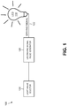
- embodiments of the invention include a stop-calibrated light source 100 created by driving a Light Emitting Diode (LED) 110 by a duty-cycle modulated driving signal 122.
- a driving signal pulse generator 120 generates the driving signal 122.
- a user may select a desired light value using a selector 130. Then, based on the user selection, the driving signal pulse generator 120 generates pulses at a particular selected frequency and duty cycle that causes the LED 110 to generate the desired amount of light.
- the driving signal pulse generator 120 outputs pulses that are discretely selectable and that each correspond to light stopped output by the LED 110. In other words, the user uses the light value selector 130 to choose the light output, measured in stops, from unity.
- the driving signal 122 provides constant current, but has a duty cycle that is reduced in steps from unity in powers of two (i.e. 1, 1/2, 1/4, etc.) to create a calibrated step change in light output of the LED 110 in 1-stop or fractional-stop increments.
- This on-off, pulse-current driving signal 122 keeps the on-current value fixed over all stop settings, thereby keeping the instantaneous power and resulting light output for each pulse constant and independent of duty cycle. In this way, the light values are not affected by temperature or differences in LEDs as compared to a multi-LED method or voltage driven duty cycle modulator. Therefore, only the duty cycle affects the average brightness of the LED 110.
- n is not restricted to integer values, allowing fractional stop changes as well as 1-stop increments.
- a user selects the stop value, n, using the selector 130, which causes the signal pulse generator 120 to generate the driving signal 122 having a duty cycle that corresponds to the selected stop value.
- the user may select an initial stop value, and then the signal pulse generator 120 automatically cycles through all of the discrete stop values that it is programmed to generate.
- the sequence of stepping through the pre-set values may be repeated many times and the individual outputs that correspond to the pre-set values may be averaged to enhance calibration accuracy. In some systems there may be up to 14 or 16 discrete stop values, while in other systems 10 or 12 stop values is sufficient.
- the electrical output from a camera pointed at the LED 110 will correspondingly step its output in a defined relation to the amount of light generated by the LED.
- the stop values generated by the pulse generator 120 may be generated in ascending or descending values.
- the calibration system 200 includes a light source, such as the LED 110 ( Fig. 1 ) placed in a container 210, such as a cube shaped box (as illustrated in Fig. 2 ), hollow sphere, or other shape that minimizes light escaping the container.
- the LED 110 is placed in the container 210, for example in a corner 212 opposite a hole 214 in one face of the container 210, as shown in Fig 2 .
- the LED 110 may be driven by the circuit illustrated in Fig. 1 , which is structured to generate light having predetermined values related to one another.
- the container 210 containing the LED 110 has a non-reflective interior, which may be black in color, and acts as a light trap to create a black surround adjacent to the LED 110 as seen by a camera 230 that is desired to be calibrated.
- This black surround created by the container 210 creates a black reference level in a video signal output of the camera 230.
- the black surround is created by trapping and absorbing ambient lighting, such as the set-lighting 220, including any ambient sunlight, which is normally reflected back to the camera 230 when not using a light trap.
- the black surround from the container 210 is used to determine a black level of the output of the camera 230 relative to the brightest parts of the scene captured by the camera, as well as the calibrated LED light source 110.
- the LED light source 110 may be a fast LED, which is capable of creating low light levels from a very narrow pulse width generated by the signal pulse generator 120 ( Fig. 1 ). For example, generating a driving signal 122 to drive the LED 110 at, for example, -10 to -11 stops means that the driving signal 122 has a very short duty cycle, which exhibits as a series of very narrow pulse widths of the driving signal. It is possible that such dim light generated by the LED 110 may not be able to be fully integrated by the camera sensor within the camera 230. To further increase the stop testing range, the camera lens of the camera 230 can be stopped down or a Neutral-Density (ND) filter of several stops may be applied. This way, cameras can be tested over the full dynamic range of the imager by combining the results with and without stopping the lens down, if necessary.
- ND Neutral-Density
- the output of the camera 230 may be displayed on a screen 240 of, for example, a waveform monitor set to capture the electrical output of the camera 230, as described in more detail below.
- a table of output values is created, with a measured output value for every discrete light value, i.e., stop value, being measured.
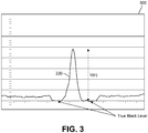
- Fig. 3 illustrates a graticule 300 of a waveform monitor (not illustrated) for measuring output values of the camera 230 when measuring various levels of light in the container 210 of Fig. 2 .
- a waveform 330 has a peak located in between two "true-black" levels. The true-black levels correspond to the light measured by the camera of the hole 214 of the container 210, while the peak level corresponds to the level of light measured by the camera at the brightest portion of the LED 110 driven at a particular stop value, as described above.
- the driving signal 122 driving the LED 110 is stopped down, as described above, the waveform 330 will correspondingly decrease.
- the black levels of the hole 214 will remain roughly the same for every stop-value measurement.
- the output of the camera 230 may be measured for each of the stop values driven by the driving signal 122. Measured values from each of the stop values may be used to generate a table, as illustrated below as Table 1.
- Table 1 n V(n) 0 695 -1 480 -2 338 -3 222 -4 144 -5 88 -6 60 -7 38 -8 26 -9 12 -10 1
- 11 stops (n), labeled 0 - -10 are illustrated in the first column.
- the second column holds measured electrical voltages, in mV, measured from the output of a camera 230 on, for example, the graticule 300 of Fig. 3 .
- the camera 230 outputs 695 mV, while, when the LED 110 ( Fig. 1 ) was driven at a -5-stop value, i.e., stopped down five stops from the full output, the output of camera 230 measures 88 mV.
- Fig. 4 These values are graphed in Fig. 4 , with the measured values indicated by the solid line 410, while the ideal values according to the defined OETF values for the camera are graphed as the dotted line 420. In this case the measured output values from the camera 230 do not identically match the ideal values.
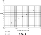
- Fig. 5 illustrates this concept in a different form of graph.
- Fig. 5 is graphed on a log 2 scale.
- the graph 500 illustrates the measured values for each stop level with a cross 510, and illustrates the ideal values for each stop with an open circle 520.
- the measured value 510 generally corresponds to the ideal value 520.
- the solid line of measured values 410 aligns closely with the dotted line of ideal values 420.
- the measured OETF response 510 from the camera 230 varies somewhat from the ideal values 520 for each.
- Embodiments of the invention may be used to compensate for the non-ideal performance of the camera 230, as described below.
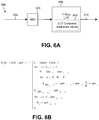
- a calibrator 600 receives an electrical signal output 602 of the camera 230 ( Fig. 2 ) and generates a log 2 weighted scale output 612 that an ideal camera would have produced, so that the light viewed by the camera 630 may be accurately measured.
- the output 612 may be fed to a waveform monitor to generate the f-stop scaled waveform display, such as that illustrated in Fig. 7 .
- the calibrator 600 includes an Analog to Digital Converter (ADC) 620, which receives the analog voltage value from the output of the camera 230 and converts it to a data value that is used to index a Look-Up Table (LUT) 650. Then, based on the particular value that the LUT 650 receives, the LUT selects and produces the desired output.
- ADC Analog to Digital Converter
- the ADC 620 illustrated in Fig. 6A is integrated in the camera 230 itself, and not a separate component outside the camera.
- the LUT 650 may also be integrated within the camera, and thus, the camera itself may be calibrated by properly populating the LUT.
- the calibrator 600 or some of its component parts, such as the LUT 650, are integrated within a test and measurement instrument, such as a waveform monitor.
- a camera 230 may couple directly to a waveform monitor to make camera signal measurements.
- the calibrator 600, or components thereof may be stand-alone components, and not embodied in either a camera nor a waveform monitor or other instrument.
- the LUT 650 is populated with values that allow a correspondence to be made from the digitized camera value from the ADC 620 to the desired output.
- the LUT 650 may be generated in several different ways. In one embodiment the ideal scaled values are determined from several variables. Once such variable is the number of stops that were selected by the user using the light value selector 130. The user may specify a 10-stop system, 12-stop system 14 stop system, etc. Another variable is the bit-depth of the ADC 620. For instance, the ADC 620 may have a 12-bit output and generate output values between 0 and 4095. Then a scale is generated corresponding to the data values of the output curve of the camera 230 as illustrated in Fig. 4 .
- Fig. 6B An example method of producing the scale values to populate the LUT 650 is illustrated in Fig. 6B .
- a scaled range of data values is assigned using the process illustrated in Fig. 6B that directly translates numerical value ranges to a stop value.
- Equation 1 The final values determined by Equation 1 and stored in LUT 650 for the particularly described system including a 700 mV maximum signal output from the camera 230, 10 non-zero stops, and a 12-bit ADC may appear as illustrated in Table 2: Table 2 max value stop 3735 0 2659 -1 1948 -2 1367 -3 977 -4 697 -5 556 -6 446 -7 386 -8 316 -9 261 -10
- the camera 230 produces an electrical value based on the amount of light being captured by the camera and according to the OETF of the camera. Then this value is translated by the ADC 620 to a value ranging between 0 and 4095, i.e., a 12-bit value.
- the value generated by the ADC 620 is used as an index value to the calibrated ideal values stored in the LUT 650, which, for this example, may be assumed to be the same as represented in Table 2.
- the 12-bit value is indexed against the stored stop values and a particular output value, from 0 to -10 stops, is selected and output by the LUT 650 as the light measured by the camera 230, as calibrated by the calibrator 600.
- the LUT 650 outputs -6 stops. In other words, the camera 230 is sensing light approximately -6 stops down from full light. If the output of the ADC were instead "1920", then the LUT 650 would output -2 stops. Such a relationship makes sense because a higher 12-bit number from the ADC 620 means there was a higher electrical input from the camera 230. The camera 230 generates a higher electrical output when there is more light, and the final output of -2 stops means that the camera 230 is sensing more light than when the output was -6 stops.
- Fig. 7 illustrates a graph 700 of output values generated by the calibrator 600 according to embodiments of the invention.
- the graph 700 includes ideal values generated by a camera 230 that has been calibrated by the process described above.
- the calibrated outputs may be an automated sequence when the light value selector 130 ( Fig. 1 ) is structured to automatically step through its pre-set values, as described above. Additionally, the sequence of stepping through the pre-set values may be repeated many times and the individual outputs averaged to enhance calibration accuracy.
- Fig. 8 illustrates a flow 800 of example operations that be used to create the LUT 650 illustrated in Fig. 6A according to embodiments of the invention.
- An operation 810 includes measuring a plurality of uncalibrated electrical outputs of a camera that respectively correspond to a plurality of known amounts of light. An example of this was described above with reference to Table 1.
- the uncalibrated outputs from the camera are stored in a table or memory generated by pointing the camera at a known amount of light. For instance, with reference to Fig. 2 above, the camera may be pointed at the LED 110 that was driven with various levels of light that vary by stops, or log 2 values from one another.
- the uncalibrated output values are stored, for example in a table or memory.
- Operation 830 creates a LUT. For example, operation 830 may first determine how many number of independent calibrated outputs will be in the correlation table, then, for every of the number of independent calibrated outputs, associate a range of uncalibrated electrical output levels. An example equation that may perform this function is illustrated as Equation 1 above. The table may appear as described above with reference to Table 2. Next, the range of uncalibrated electrical output levels and their associated calibrated outputs are stored in a LUT in operation 840.
- This LUT may be stored in computer memory (e.g., Read Only Memory (ROM) or in Random Access Memory (RAM) or in another storage medium.
- the LUT may exist in a test and measurement device, such as a waveform monitor, for example.
- An embodiment of the technologies disclosed herein may include any one or more, and any combination of, the examples described below.
Landscapes
- Engineering & Computer Science (AREA)
- Health & Medical Sciences (AREA)
- Biomedical Technology (AREA)
- General Health & Medical Sciences (AREA)
- Multimedia (AREA)
- Signal Processing (AREA)
- Physics & Mathematics (AREA)
- General Physics & Mathematics (AREA)
- Testing, Inspecting, Measuring Of Stereoscopic Televisions And Televisions (AREA)
- Studio Devices (AREA)
Applications Claiming Priority (2)
| Application Number | Priority Date | Filing Date | Title |
|---|---|---|---|
| US201662291795P | 2016-02-05 | 2016-02-05 | |
| US15/384,077 US20170230650A1 (en) | 2016-02-05 | 2016-12-19 | Camera stop calibrator |
Publications (2)
| Publication Number | Publication Date |
|---|---|
| EP3203734A2 true EP3203734A2 (fr) | 2017-08-09 |
| EP3203734A3 EP3203734A3 (fr) | 2017-08-23 |
Family
ID=58094163
Family Applications (1)
| Application Number | Title | Priority Date | Filing Date |
|---|---|---|---|
| EP17154862.1A Withdrawn EP3203734A3 (fr) | 2016-02-05 | 2017-02-06 | Étalonnage de caméra |
Country Status (4)
| Country | Link |
|---|---|
| US (1) | US20170230650A1 (fr) |
| EP (1) | EP3203734A3 (fr) |
| JP (1) | JP2017188872A (fr) |
| CN (1) | CN107046641A (fr) |
Cited By (1)
| Publication number | Priority date | Publication date | Assignee | Title |
|---|---|---|---|---|
| CN115079505A (zh) * | 2022-05-31 | 2022-09-20 | 合肥埃科光电科技股份有限公司 | 基于泰伯效应的棱镜分光多光谱相机匹配校准装置及方法 |
Families Citing this family (2)
| Publication number | Priority date | Publication date | Assignee | Title |
|---|---|---|---|---|
| JP2020148747A (ja) * | 2019-03-15 | 2020-09-17 | 株式会社リコー | 物体検出装置 |
| US11245845B2 (en) | 2020-06-04 | 2022-02-08 | Hand Held Products, Inc. | Systems and methods for operating an imaging device |
Family Cites Families (6)
| Publication number | Priority date | Publication date | Assignee | Title |
|---|---|---|---|---|
| US20050225264A1 (en) * | 2004-03-30 | 2005-10-13 | Kemp William H | LED lamp with color and brightness controller for use in wet, electrically hazardous bathing environments |
| KR100862507B1 (ko) * | 2007-06-20 | 2008-10-08 | 삼성전기주식회사 | Led 구동 디바이스 |
| US8154753B2 (en) * | 2008-10-29 | 2012-04-10 | Thx, Ltd. | Method and system for providing access to image system services |
| US20100188006A1 (en) * | 2009-01-28 | 2010-07-29 | Garrett Joseph Young | Dimming alternating current light emitting diodes |
| US8994714B2 (en) * | 2010-09-23 | 2015-03-31 | Dolby Laboratories Licensing Corporation | Method and system for display calibration with feedback determined by a camera device |
| US20120314086A1 (en) * | 2011-06-08 | 2012-12-13 | Apple Inc. | Camera test and calibration based on spectral monitoring of light |
-
2016
- 2016-12-19 US US15/384,077 patent/US20170230650A1/en not_active Abandoned
-
2017
- 2017-02-05 CN CN201710227027.8A patent/CN107046641A/zh active Pending
- 2017-02-06 EP EP17154862.1A patent/EP3203734A3/fr not_active Withdrawn
- 2017-02-06 JP JP2017019835A patent/JP2017188872A/ja active Pending
Non-Patent Citations (1)
| Title |
|---|
| None |
Cited By (2)
| Publication number | Priority date | Publication date | Assignee | Title |
|---|---|---|---|---|
| CN115079505A (zh) * | 2022-05-31 | 2022-09-20 | 合肥埃科光电科技股份有限公司 | 基于泰伯效应的棱镜分光多光谱相机匹配校准装置及方法 |
| CN115079505B (zh) * | 2022-05-31 | 2024-05-10 | 合肥埃科光电科技股份有限公司 | 基于泰伯效应的棱镜分光多光谱相机匹配校准装置及方法 |
Also Published As
| Publication number | Publication date |
|---|---|
| EP3203734A3 (fr) | 2017-08-23 |
| JP2017188872A (ja) | 2017-10-12 |
| US20170230650A1 (en) | 2017-08-10 |
| CN107046641A (zh) | 2017-08-15 |
Similar Documents
| Publication | Publication Date | Title |
|---|---|---|
| US7697031B2 (en) | Intelligent light source with synchronization with a digital camera | |
| US10085611B2 (en) | Light source apparatus for driving light sources based on generated light adjustment information | |
| US8534914B2 (en) | System and method for estimating the junction temperature of a light emitting diode | |
| EP2273851A2 (fr) | Système et procédé pour le contrôle de grappe de DEL | |
| KR102581846B1 (ko) | 표시 패널의 보상 데이터 생성 방법 및 장치 | |
| RU2015141766A (ru) | Устройства, способы и системы для измерения и обнаружения электрического разряда | |
| EP3471403B1 (fr) | Téléviseur hdr et procédé de gradation locale | |
| CN106324965B (zh) | Dlp激光投影机自动白平衡调整装置及方法 | |
| EP3203734A2 (fr) | Étalonnage de caméra | |
| CN105164550A (zh) | 测距装置以及测距方法 | |
| CN109788622B (zh) | 光源控制装置、光源控制方法以及飞行时间传感器 | |
| US20110025907A1 (en) | Camera Head Separated Type Camera Device | |
| US7990426B2 (en) | Phase adjusting device and digital camera | |
| JP5089501B2 (ja) | 液晶ディスプレイ装置、発光装置、発光バランス制御装置および発光強度検出装置 | |
| KR20180014333A (ko) | 표시 패널의 휘도 보상 방법 및 장치 | |
| US9324146B2 (en) | Photometric and radiometric calibration using optical feedback | |
| KR20090058363A (ko) | 발광 다이오드의 순방향 전압을 이용하여 광학 파라미터를보상하는 디스플레이 장치 및 디스플레이 방법 | |
| TWI442377B (zh) | Liquid crystal backlight with dimming circuit | |
| US20130176465A1 (en) | Image pickup apparatus and method of forming image data | |
| JP2007093477A (ja) | 色測定装置の校正方法および校正装置、色測定方法、色測定装置 | |
| US9985209B2 (en) | Method for testing lifetime characteristics of display panel, and method for manufacturing display panel | |
| JP2024043698A (ja) | 表示方法、表示システム、及びプログラム | |
| US9781802B1 (en) | Illumination correcting method and apparatus for at least one light source board | |
| US20250046272A1 (en) | Device and method for measuring overshoot without distortion in display | |
| EP0562974A1 (fr) | Procédé de mesure soustractif et dispositif pour mesurer l'intensité lumineuse d'un tube cathodique |
Legal Events
| Date | Code | Title | Description |
|---|---|---|---|
| PUAI | Public reference made under article 153(3) epc to a published international application that has entered the european phase |
Free format text: ORIGINAL CODE: 0009012 |
|
| STAA | Information on the status of an ep patent application or granted ep patent |
Free format text: STATUS: THE APPLICATION HAS BEEN PUBLISHED |
|
| PUAL | Search report despatched |
Free format text: ORIGINAL CODE: 0009013 |
|
| AK | Designated contracting states |
Kind code of ref document: A2 Designated state(s): AL AT BE BG CH CY CZ DE DK EE ES FI FR GB GR HR HU IE IS IT LI LT LU LV MC MK MT NL NO PL PT RO RS SE SI SK SM TR |
|
| AX | Request for extension of the european patent |
Extension state: BA ME |
|
| AK | Designated contracting states |
Kind code of ref document: A3 Designated state(s): AL AT BE BG CH CY CZ DE DK EE ES FI FR GB GR HR HU IE IS IT LI LT LU LV MC MK MT NL NO PL PT RO RS SE SI SK SM TR |
|
| AX | Request for extension of the european patent |
Extension state: BA ME |
|
| RIC1 | Information provided on ipc code assigned before grant |
Ipc: H05B 33/08 20060101ALI20170718BHEP Ipc: G03B 43/00 20060101ALI20170718BHEP Ipc: H04N 17/00 20060101AFI20170718BHEP |
|
| STAA | Information on the status of an ep patent application or granted ep patent |
Free format text: STATUS: REQUEST FOR EXAMINATION WAS MADE |
|
| 17P | Request for examination filed |
Effective date: 20170901 |
|
| RBV | Designated contracting states (corrected) |
Designated state(s): AL AT BE BG CH CY CZ DE DK EE ES FI FR GB GR HR HU IE IS IT LI LT LU LV MC MK MT NL NO PL PT RO RS SE SI SK SM TR |
|
| STAA | Information on the status of an ep patent application or granted ep patent |
Free format text: STATUS: EXAMINATION IS IN PROGRESS |
|
| 17Q | First examination report despatched |
Effective date: 20180504 |
|
| GRAP | Despatch of communication of intention to grant a patent |
Free format text: ORIGINAL CODE: EPIDOSNIGR1 |
|
| STAA | Information on the status of an ep patent application or granted ep patent |
Free format text: STATUS: GRANT OF PATENT IS INTENDED |
|
| INTG | Intention to grant announced |
Effective date: 20200131 |
|
| STAA | Information on the status of an ep patent application or granted ep patent |
Free format text: STATUS: THE APPLICATION IS DEEMED TO BE WITHDRAWN |
|
| 18D | Application deemed to be withdrawn |
Effective date: 20200611 |