EP3205979A1 - Selbstschwingungsschaltung - Google Patents
Selbstschwingungsschaltung Download PDFInfo
- Publication number
- EP3205979A1 EP3205979A1 EP16155454.8A EP16155454A EP3205979A1 EP 3205979 A1 EP3205979 A1 EP 3205979A1 EP 16155454 A EP16155454 A EP 16155454A EP 3205979 A1 EP3205979 A1 EP 3205979A1
- Authority
- EP
- European Patent Office
- Prior art keywords
- vibrator
- self
- circuit
- oscillation circuit
- signal
- Prior art date
- Legal status (The legal status is an assumption and is not a legal conclusion. Google has not performed a legal analysis and makes no representation as to the accuracy of the status listed.)
- Granted
Links
Images


Classifications
-
- H—ELECTRICITY
- H03—ELECTRONIC CIRCUITRY
- H03B—GENERATION OF OSCILLATIONS, DIRECTLY OR BY FREQUENCY-CHANGING, BY CIRCUITS EMPLOYING ACTIVE ELEMENTS WHICH OPERATE IN A NON-SWITCHING MANNER; GENERATION OF NOISE BY SUCH CIRCUITS
- H03B5/00—Generation of oscillations using amplifier with regenerative feedback from output to input
- H03B5/08—Generation of oscillations using amplifier with regenerative feedback from output to input with frequency-determining element comprising lumped inductance and capacitance
- H03B5/12—Generation of oscillations using amplifier with regenerative feedback from output to input with frequency-determining element comprising lumped inductance and capacitance active element in amplifier being semiconductor device
- H03B5/1228—Generation of oscillations using amplifier with regenerative feedback from output to input with frequency-determining element comprising lumped inductance and capacitance active element in amplifier being semiconductor device the amplifier comprising one or more field effect transistors
-
- H—ELECTRICITY
- H03—ELECTRONIC CIRCUITRY
- H03B—GENERATION OF OSCILLATIONS, DIRECTLY OR BY FREQUENCY-CHANGING, BY CIRCUITS EMPLOYING ACTIVE ELEMENTS WHICH OPERATE IN A NON-SWITCHING MANNER; GENERATION OF NOISE BY SUCH CIRCUITS
- H03B5/00—Generation of oscillations using amplifier with regenerative feedback from output to input
- H03B5/08—Generation of oscillations using amplifier with regenerative feedback from output to input with frequency-determining element comprising lumped inductance and capacitance
- H03B5/12—Generation of oscillations using amplifier with regenerative feedback from output to input with frequency-determining element comprising lumped inductance and capacitance active element in amplifier being semiconductor device
- H03B5/1206—Generation of oscillations using amplifier with regenerative feedback from output to input with frequency-determining element comprising lumped inductance and capacitance active element in amplifier being semiconductor device using multiple transistors for amplification
- H03B5/1212—Generation of oscillations using amplifier with regenerative feedback from output to input with frequency-determining element comprising lumped inductance and capacitance active element in amplifier being semiconductor device using multiple transistors for amplification the amplifier comprising a pair of transistors, wherein an output terminal of each being connected to an input terminal of the other, e.g. a cross coupled pair
-
- H—ELECTRICITY
- H03—ELECTRONIC CIRCUITRY
- H03B—GENERATION OF OSCILLATIONS, DIRECTLY OR BY FREQUENCY-CHANGING, BY CIRCUITS EMPLOYING ACTIVE ELEMENTS WHICH OPERATE IN A NON-SWITCHING MANNER; GENERATION OF NOISE BY SUCH CIRCUITS
- H03B5/00—Generation of oscillations using amplifier with regenerative feedback from output to input
- H03B5/08—Generation of oscillations using amplifier with regenerative feedback from output to input with frequency-determining element comprising lumped inductance and capacitance
- H03B5/12—Generation of oscillations using amplifier with regenerative feedback from output to input with frequency-determining element comprising lumped inductance and capacitance active element in amplifier being semiconductor device
- H03B5/1237—Generation of oscillations using amplifier with regenerative feedback from output to input with frequency-determining element comprising lumped inductance and capacitance active element in amplifier being semiconductor device comprising means for varying the frequency of the generator
- H03B5/124—Generation of oscillations using amplifier with regenerative feedback from output to input with frequency-determining element comprising lumped inductance and capacitance active element in amplifier being semiconductor device comprising means for varying the frequency of the generator the means comprising a voltage dependent capacitance
- H03B5/1243—Generation of oscillations using amplifier with regenerative feedback from output to input with frequency-determining element comprising lumped inductance and capacitance active element in amplifier being semiconductor device comprising means for varying the frequency of the generator the means comprising a voltage dependent capacitance the means comprising voltage variable capacitance diodes
-
- H—ELECTRICITY
- H03—ELECTRONIC CIRCUITRY
- H03B—GENERATION OF OSCILLATIONS, DIRECTLY OR BY FREQUENCY-CHANGING, BY CIRCUITS EMPLOYING ACTIVE ELEMENTS WHICH OPERATE IN A NON-SWITCHING MANNER; GENERATION OF NOISE BY SUCH CIRCUITS
- H03B5/00—Generation of oscillations using amplifier with regenerative feedback from output to input
- H03B5/30—Generation of oscillations using amplifier with regenerative feedback from output to input with frequency-determining element being electromechanical resonator
Definitions
- the present invention relates to a self-oscillation circuit for oscillating a vibrator by a positive feedback circuit.
- a capacitive vibration type pressure/differential pressure sensor or the like includes a self-oscillation circuit for oscillating a vibrator at a resonance frequency.
- Fig. 8 is a view showing a configuration example of a related-art capacitive vibration type self-oscillation circuit.
- a self-oscillation circuit 500 includes a positive feedback circuit for oscillating a vibrator 511 and a negative feedback circuit for controlling oscillation amplitude of the vibrator 511.
- the positive feedback circuit is formed in a loop passing through the vibrator 511, a second fixed electrode 513, an I/V converter 520, an inverting amplifier 530 and a variable-gain amplifier 560 from a first fixed electrode 512.
- the vibrator 511 is vacuum-sealed in order to increase a value of Q.
- the negative feedback circuit is formed in a circuit passing through an absolute value circuit 540 for detecting an absolute value of a signal outputted from the inverting amplifier 530, an error amplifier 550, and the variable-gain amplifier 560.
- the vibrator 511 is fixed to a GND potential, and a bias voltage VBIAS is applied to the first fixed electrode 512 and the second fixed electrode 513 via a DC voltage source. At this time, a charge corresponding to capacitance is charged between the vibrator 511 and the first fixed electrode 512, and between the vibrator 511 and the second fixed electrode 513.
- an output voltage VGAO of the variable-gain amplifier 560 is applied to the first fixed electrode 512.
- the vibrator 511 vibrates in accordance with the potential change of the first fixed electrode 512.
- a current output signal from the second fixed electrode 513 is inputted to the I/V converter 520 and is outputted as a voltage signal IVO.
- the voltage signal IVO is inverted and amplified in the inverting amplifier 530 and is outputted as a voltage signal INVO.
- the voltage signal INVO is amplified in the variable-gain amplifier 560 and is applied, as the voltage signal VGAO, to the first fixed electrode 512.
- Such positive feedback circuit allows the vibrator 511 to vibrate at its own resonance frequency.
- the amplitude of the voltage signal INVO outputted from the inverting amplifier 530 is detected by the absolute value circuit 540.
- the absolute value circuit 540 can be configured by using a full-wave rectifier circuit or the like.
- a voltage signal ABSO outputted from the absolute value circuit 540 corresponds to oscillation amplitude of the vibrator 511.
- a difference between the voltage signal ABSO and a reference voltage VCONT is detected, as an error signal ERRO, in the error amplifier 550, and the gain of the variable-gain amplifier 560 is changed by the error signal ERRO.
- the gain of the variable-gain amplifier 560 is increased when the amplitude of the vibrator 511 is small and the error signal ERRO is great, and the gain of the variable-gain amplifier 560 is decreased when the amplitude of the vibrator 511 is great and the error signal ERRO is small.
- the gain of the variable-gain amplifier 560 is adjusted, the amplitude of the vibrator 511 is normally controlled to be constant.
- Patent Document 1 International Publication WO 2011/102062
- self-oscillation circuit 500 When such self-oscillation circuit 500 is applied to an apparatus that requires low power consumption, such as, for example, two-wire type instrument, it is necessary to constitute the self-oscillation circuit by an ASIC where it is easy to achieve low power consumption. The reason is that it is difficult to satisfy the low power consumption specification when the self-oscillation circuit is configured by a discrete component.
- a gain of the variable-gain amplifier 560 which is used in the positive feedback, is changed by the output of the negative feedback circuit. Therefore, the positive feedback circuit and the negative feedback circuit have a mutually dependent relationship, and hence, the interface therebetween becomes complicated. Accordingly, a strict adjustment between the positive feedback circuit and the negative feedback circuit is required. For example, when the design changes to the I/V converter 520 and the inverting amplifier 530 occur, the design of the variable-gain amplifier 560 should be also changed. This causes an increase in the design man-hours and acts as a barrier to the ASIC.
- Exemplary embodiments of the invention provide a self-oscillation circuit without using a variable-gain amplifier that complicates an interface between a positive feedback circuit and a negative feedback circuit.
- a self-oscillation circuit comprises:
- the self-oscillation circuit may further comprise:
- the self-oscillation circuit may further comprise:
- the negative feedback circuit may generate the pulse-width-modulated signal such that the greater a difference between the value corresponding to the amplitude of the vibrator and the reference value is, the longer a pulse width is.
- the negative feedback circuit may include an error amplifier which compares the value corresponding to the amplitude of the vibrator with the reference value to output an error signal, and a PWM unit which performs pulse-width-modulation of the error signal.
- the PWM unit may include a triangular wave oscillator which outputs a triangular wave having a frequency lower than the vibration frequency of the vibrator, and a comparator which compares the error signal with the triangular wave to generate the pulse-width-modulated signal.
- the negative feedback circuit may include an AD converter which digitally converts the value corresponding to the amplitude of the vibrator, a digital error detection unit which compares the digitized value with the reference value to detect an error, a digital PWM unit which performs pulse width modulation of the detected error.
- the digital error detection unit may include a subtractor which calculates a difference between the digitized value and the reference value and a digital filter which controls the digital PWM unit according to the difference.
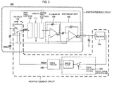
- Fig. 1 is a view showing a configuration of a self-oscillation circuit 100 according to a first embodiment of the present invention.
- the self-oscillation circuit of the present invention is not limited to a capacitive vibration type self-oscillation circuit, but can be applied to various self-oscillation circuits having a positive feedback circuit.
- the self-oscillation circuit 100 of the first embodiment includes a positive feedback circuit for oscillating a vibrator 111, and a negative feedback circuit for controlling oscillation amplitude of the vibrator 111.
- the positive feedback circuit is formed in a loop passing through the vibrator 111, a second fixed electrode 113, an I/V converter 120, an inverting amplifier 130 and a SW circuit 170 from a first fixed electrode 112.
- the vibrator 111 is vacuum-sealed in order to increase a value of Q.
- the first fixed electrode 112, the vibrator 111 and the second fixed electrode 113 constitute a vibration unit.
- a positive feedback path is configured by a path that extends from an output of the inverting amplifier 130 to an input of the first fixed electrode 112 via the SW circuit 170.
- the negative feedback circuit is formed in a circuit passing through an absolute value circuit 140 for detecting an absolute value of a voltage signal INVO outputted from the inverting amplifier 130, an error amplifier 150, a PWM unit 160, and the SW circuit 170.
- the SW circuit 170 is switched and controlled by an output signal PWMO of the PWM unit 160. Specifically, when the output signal PWMO is H, the voltage signal INVO outputted from the inverting amplifier 130 is fed back to the first fixed electrode 112 to form a positive feedback loop of the positive feedback circuit. Further, when the output signal PWMO is L, the positive feedback loop of the positive feedback circuit is released.
- the vibrator 111 is fixed to a GND potential, and a bias voltage VBIAS is applied to the first fixed electrode 112 and the second fixed electrode 113 via a DC voltage source, regardless of the state of the SW circuit 170. At this time, a charge corresponding to capacitance is charged between the vibrator 111 and the first fixed electrode 112, and between the vibrator 111 and the second fixed electrode 113.
- the output signal PWMO is H
- the positive feedback loop is formed by the SW circuit 170. Therefore, in addition to the bias voltage VBIAS, the voltage signal INVO outputted from the inverting amplifier 130 is applied to the first fixed electrode 112 and the vibrator 111 vibrates according to the potential change of the first fixed electrode 112.
- a current output signal from the second fixed electrode 113 is inputted to the I/V converter 120 and is outputted as a voltage signal IVO.
- the voltage signal IVO is inverted and amplified in the inverting amplifier 130 and is outputted as the voltage signal INVO.
- Such positive feedback circuit allows the vibrator 111 to vibrate at its own resonance frequency.
- the amplitude of the voltage signal INVO outputted from the inverting amplifier 130 is detected by the absolute value circuit 140.
- the absolute value circuit 140 can be configured by using a full-wave rectifier circuit or the like.
- a voltage signal ABSO outputted from the absolute value circuit 140 corresponds to the oscillation amplitude of the vibrator 111.
- a difference between the voltage signal ABSO and a reference voltage VCONT is detected, as an error signal ERRO, in the error amplifier 150.
- the error signal ERRO is pulse-width-modulated by the PWM unit 160 and is outputted as a PWMO signal.
- the error signal ERRO can be compared with a triangular wave (a saw-toothed wave) TRI by a comparator 161, thereby generating the PWMO signal.
- a triangular wave a saw-toothed wave
- the frequency of the pulse width modulation i.e., the frequency of the triangular wave
- a frequency lower than the resonance frequency of the vibrator 111 is used. The reason is that a positive feedback loop formation period is sufficiently secured with respect to the vibration cycle and the vibrator 111 is stably oscillated.
- the PWMO signal When the PWMO signal is H, i.e., when the error signal ERRO is greater than the triangular wave TRI, the positive feedback loop is formed, and thus, the amplitude of the vibrator 111 is grown.
- the PWMO signal is L, i.e., when the error signal ERRO is smaller than the triangular wave TRI, the positive feedback loop is released, and thus, the amplitude of the vibrator 111 is attenuated. As the growth and attenuation of the amplitude is repeated, the amplitude of the vibrator 111 is normally controlled to be constant.
- the Q of the vibrator 111 is generally designed to be relatively high. Therefore, with respect to the oscillation cycle of the vibrator 111, the growth and attenuation of the amplitude is very gentle. Accordingly, even when the vibrator 111 is intermittently operated by the SW circuit 170, the hunting width of the amplitude of the vibrator 111 can be reduced and the amplitude can be normally controlled to be almost constant.
- the variable-gain amplifier that complicates the interface between the positive feedback circuit and the negative feedback circuit is not necessary, and the positive feedback circuit and the negative feedback circuit are disconnected, so that the interface adjustment between the circuits is simplified. That is, the characteristics on the positive feedback circuit side are uniquely determined by the design of the I/V converter 120 and the inverting amplifier 130, and the characteristics on the negative feedback circuit side are uniquely determined by the design of the error amplifier 150 and the PWM unit 160. In this way, the positive feedback circuit and the negative feedback circuit can be independently adjusted. As a result, the design man-hours can be reduced and the ASIC is easily achieved.
- the PWM unit 160 which can be configured by a versatile comparator and a versatile triangular wave oscillator, is used. Therefore, it is also possible to achieve the easy mounting, the low voltage and the low consumption power.
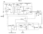
- Fig. 3 is a view showing a configuration of a self-oscillation circuit 200 according to a second embodiment of the present invention.
- the self-oscillation circuit 200 of the second embodiment also includes a positive feedback circuit for oscillating the vibrator 111, and a negative feedback circuit for controlling oscillation amplitude of the vibrator 111.
- the negative feedback circuit is digitized.
- the positive feedback circuit is similar to that of the first embodiment, the positive feedback circuit is denoted by the same reference numeral. Namely, the positive feedback circuit is formed in a loop passing through the vibrator 111, the second fixed electrode 113, the I/V converter 120, the inverting amplifier 130 and the SW circuit 170 from the first fixed electrode 112.
- the negative feedback circuit is formed in a circuit passing through an AD converter 210 for digitally converting the voltage signal INVO outputted from the inverting amplifier 130, a digital error detection unit 220 for comparing the digitized value with a reference value and detecting an error, a digital PWM unit 230 for performing the pulse width modulation of the detected error, and the SW circuit 170.
- the digital error detection unit 220 can be configured by a subtractor for calculating a difference between the digitized value and the digital reference voltage and a digital filter for controlling the digital PWM unit 230 according to the error.
- the SW circuit 170 is switched and controlled by the output signal PWMO of the digital PWM unit 230. Specifically, the positive feedback loop of the positive feedback circuit is formed when the output signal PWMO is H, and the positive feedback loop of the positive feedback circuit is released when the output signal PWMO is L.
- the negative feedback circuit of the self-oscillation circuit 200 of the second embodiment is digitized, a basic operation principle of the self-oscillation circuit 200 is similar to the self-oscillation circuit 100 of the first embodiment. Since, in addition to the characteristics of the self-oscillation circuit 100 of the first embodiment, the self-oscillation circuit 200 of the second embodiment is configured such that an analog circuit element is omitted, the design man-hours can be further reduced. Further, since the integration degree of the analog circuit in the ASIC is lowered, the production cost can be reduced.
- Fig. 4 is a view showing a configuration of a self-oscillation circuit 300 according to a third embodiment of the present invention.
- the self-oscillation circuit 300 of the third embodiment has a configuration that a synchronization unit 180 is additionally provided to the self-oscillation circuit 100 of the first embodiment.
- the synchronization unit 180 may be additionally provided to the self-oscillation circuit 200 of the second embodiment.
- the synchronization unit 180 includes a comparator and a D-FF and is configured such that the SW circuit 170 is switched at the timing when the voltage signal INVO (AC component) outputted from the inverting amplifier 130 is changed from negative to positive. Specifically, at the timing when the voltage signal INVO (AC component) is changed from negative to positive, i.e., when a voltage signal SWO is equal to the bias voltage VBIAS, the comparator outputs a CMPO2 signal (voltage rise) to operate the D-FF. Further, the SW circuit 170 is switched by a D-FFQ signal outputted from the D-FF. It is noted that the switching may be performed at the timing when the voltage signal INVO is changed from positive to negative or at the timing of every half cycle.
- the switching of the SW circuit 170 is not synchronized with the vibration of the vibrator 111. Therefore, at the time of the switching of the SW circuit 170, sudden variation occurs in the voltage signal SWO applied to the first fixed electrode 112, and hence, the voltage signal SWO is often disturbed.
- the switching of the SW circuit 170 is synchronized with the vibration of the vibrator 111, as shown in Fig. 5 .
- the SW circuit 170 is switched when the voltage signal SWO is equal to the bias voltage VBIAS.
- VBIAS bias voltage
- the bias voltage VBIAS is applied to the first fixed electrode 112 via the SW circuit 170, as shown in Fig. 6A .
- both an H terminal and an L terminal of the SW circuit 170 are connected to a DC voltage source.
- the bias voltage VBIAS may be applied to the first fixed electrode 112 without passing through the SW circuit 170, as shown in Fig. 6B .
- the L terminal of the SW circuit 170 may be connected to the DC voltage source or may not be connected to a DC voltage source by being floated, as shown in Fig. 6C .
- a somewhat large parasitic capacitance (e.g., about 30pF) is present between the first fixed electrode 112 and the GND. Therefore, it is necessary to supply the inverting amplifier 130 with a current for driving the parasitic capacitance. This is a factor of increasing the consumption current.
- a buffer 190 having an enable function is placed between the inverting amplifier 130 and the SW circuit 170. Only when the signal PWMO is H, the buffer 190 is in an enable state to secure the drive capacity. Further, when the signal PWMO is L, the buffer 190 is in a disable state and the current is not consumed in the buffer 190. In this way, it is possible to reduce the consumption power.
- the buffer 190 having the enable function can be applied to all of the above-described embodiments.
Landscapes
- Oscillators With Electromechanical Resonators (AREA)
- Gyroscopes (AREA)
Priority Applications (1)
| Application Number | Priority Date | Filing Date | Title |
|---|---|---|---|
| EP16155454.8A EP3205979B1 (de) | 2016-02-12 | 2016-02-12 | Selbstschwingungsschaltung |
Applications Claiming Priority (1)
| Application Number | Priority Date | Filing Date | Title |
|---|---|---|---|
| EP16155454.8A EP3205979B1 (de) | 2016-02-12 | 2016-02-12 | Selbstschwingungsschaltung |
Publications (2)
| Publication Number | Publication Date |
|---|---|
| EP3205979A1 true EP3205979A1 (de) | 2017-08-16 |
| EP3205979B1 EP3205979B1 (de) | 2022-06-01 |
Family
ID=55357903
Family Applications (1)
| Application Number | Title | Priority Date | Filing Date |
|---|---|---|---|
| EP16155454.8A Active EP3205979B1 (de) | 2016-02-12 | 2016-02-12 | Selbstschwingungsschaltung |
Country Status (1)
| Country | Link |
|---|---|
| EP (1) | EP3205979B1 (de) |
Citations (5)
| Publication number | Priority date | Publication date | Assignee | Title |
|---|---|---|---|---|
| EP0718631A2 (de) * | 1994-12-22 | 1996-06-26 | Murata Manufacturing Co., Ltd. | Kapazitiver Beschleunigungsaufnehmer mit elektrostatischem Servosystem |
| US20080297264A1 (en) * | 2005-01-05 | 2008-12-04 | Hans-Dieter Schwarz | Oscillating Circuit |
| WO2011102062A1 (ja) | 2010-02-17 | 2011-08-25 | 株式会社村田製作所 | 振動型慣性力センサ |
| US20120242389A1 (en) * | 2011-03-25 | 2012-09-27 | Kabushiki Kaisha Toshiba | Sensor control circuit and sensor system |
| US20140174178A1 (en) * | 2012-12-21 | 2014-06-26 | Samsung Electro-Mechanics Co., Ltd. | Gain control device of gyro sensor driving signal and gain control method thereof |
-
2016
- 2016-02-12 EP EP16155454.8A patent/EP3205979B1/de active Active
Patent Citations (6)
| Publication number | Priority date | Publication date | Assignee | Title |
|---|---|---|---|---|
| EP0718631A2 (de) * | 1994-12-22 | 1996-06-26 | Murata Manufacturing Co., Ltd. | Kapazitiver Beschleunigungsaufnehmer mit elektrostatischem Servosystem |
| US20080297264A1 (en) * | 2005-01-05 | 2008-12-04 | Hans-Dieter Schwarz | Oscillating Circuit |
| WO2011102062A1 (ja) | 2010-02-17 | 2011-08-25 | 株式会社村田製作所 | 振動型慣性力センサ |
| US20120291550A1 (en) * | 2010-02-17 | 2012-11-22 | Asahi Kasei Microdevices Corporation | Oscillation type inertia force sensor |
| US20120242389A1 (en) * | 2011-03-25 | 2012-09-27 | Kabushiki Kaisha Toshiba | Sensor control circuit and sensor system |
| US20140174178A1 (en) * | 2012-12-21 | 2014-06-26 | Samsung Electro-Mechanics Co., Ltd. | Gain control device of gyro sensor driving signal and gain control method thereof |
Also Published As
| Publication number | Publication date |
|---|---|
| EP3205979B1 (de) | 2022-06-01 |
Similar Documents
| Publication | Publication Date | Title |
|---|---|---|
| JP5362096B2 (ja) | 振動型慣性力センサ | |
| US9310203B2 (en) | Physical quantity sensor | |
| JP6410827B2 (ja) | 負インピーダンス制御ループを備えた共振インピーダンス感知 | |
| US8925383B2 (en) | Angular speed sensor | |
| KR20120042861A (ko) | 각속도 센서와, 그것에 이용되는 동기 검파 회로 | |
| US8653901B2 (en) | Oscillator and control circuit thereof | |
| US8656775B2 (en) | Vibratory gyro-sensor and vibratory gyro circuit | |
| US9742417B1 (en) | Self-oscillation circuit | |
| EP3205979B1 (de) | Selbstschwingungsschaltung | |
| WO2020008868A1 (ja) | 超音波センサ | |
| JP6237532B2 (ja) | 自励発振回路 | |
| CN107104637B (zh) | 自振荡电路 | |
| JP6709497B2 (ja) | 自励発振回路 | |
| JP5362097B2 (ja) | 振動型慣性力センサ | |
| US9614513B2 (en) | Vibration generation apparatus | |
| KR20140143651A (ko) | Mems 공진 센서 및 mems 공진 센서의 제어 방법 | |
| KR100881155B1 (ko) | 다중 전원 혼합형 증폭기 | |
| JP4232280B2 (ja) | 磁気インピーダンスセンサ回路 | |
| CN212133682U (zh) | 一种陀螺仪系统驱动装置 | |
| JP5344955B2 (ja) | 固体振動子発振回路およびこれを用いた物理量センサ | |
| KR101910420B1 (ko) | 자이로스코프 시스템의 구동장치 | |
| US9645122B2 (en) | Vibration generation apparatus | |
| JP2021083303A (ja) | Psrrを改善したチャージポンプ回路および高電圧生成方法 | |
| JP2008157766A (ja) | 加速度検出装置 | |
| JP2010175503A (ja) | 同期検波回路及びこれを用いた角速度センサ |
Legal Events
| Date | Code | Title | Description |
|---|---|---|---|
| PUAI | Public reference made under article 153(3) epc to a published international application that has entered the european phase |
Free format text: ORIGINAL CODE: 0009012 |
|
| STAA | Information on the status of an ep patent application or granted ep patent |
Free format text: STATUS: THE APPLICATION HAS BEEN PUBLISHED |
|
| AK | Designated contracting states |
Kind code of ref document: A1 Designated state(s): AL AT BE BG CH CY CZ DE DK EE ES FI FR GB GR HR HU IE IS IT LI LT LU LV MC MK MT NL NO PL PT RO RS SE SI SK SM TR |
|
| AX | Request for extension of the european patent |
Extension state: BA ME |
|
| STAA | Information on the status of an ep patent application or granted ep patent |
Free format text: STATUS: REQUEST FOR EXAMINATION WAS MADE |
|
| 17P | Request for examination filed |
Effective date: 20170901 |
|
| RBV | Designated contracting states (corrected) |
Designated state(s): AL AT BE BG CH CY CZ DE DK EE ES FI FR GB GR HR HU IE IS IT LI LT LU LV MC MK MT NL NO PL PT RO RS SE SI SK SM TR |
|
| STAA | Information on the status of an ep patent application or granted ep patent |
Free format text: STATUS: EXAMINATION IS IN PROGRESS |
|
| 17Q | First examination report despatched |
Effective date: 20191008 |
|
| REG | Reference to a national code |
Ref country code: DE Ref legal event code: R079 Ref document number: 602016072467 Country of ref document: DE Free format text: PREVIOUS MAIN CLASS: G01C0019577600 Ipc: H03B0005120000 |
|
| RIC1 | Information provided on ipc code assigned before grant |
Ipc: H03B 5/30 20060101ALI20211022BHEP Ipc: H03B 5/12 20060101AFI20211022BHEP |
|
| GRAP | Despatch of communication of intention to grant a patent |
Free format text: ORIGINAL CODE: EPIDOSNIGR1 |
|
| STAA | Information on the status of an ep patent application or granted ep patent |
Free format text: STATUS: GRANT OF PATENT IS INTENDED |
|
| INTG | Intention to grant announced |
Effective date: 20211208 |
|
| GRAS | Grant fee paid |
Free format text: ORIGINAL CODE: EPIDOSNIGR3 |
|
| GRAA | (expected) grant |
Free format text: ORIGINAL CODE: 0009210 |
|
| STAA | Information on the status of an ep patent application or granted ep patent |
Free format text: STATUS: THE PATENT HAS BEEN GRANTED |
|
| AK | Designated contracting states |
Kind code of ref document: B1 Designated state(s): AL AT BE BG CH CY CZ DE DK EE ES FI FR GB GR HR HU IE IS IT LI LT LU LV MC MK MT NL NO PL PT RO RS SE SI SK SM TR |
|
| REG | Reference to a national code |
Ref country code: GB Ref legal event code: FG4D |
|
| REG | Reference to a national code |
Ref country code: AT Ref legal event code: REF Ref document number: 1496096 Country of ref document: AT Kind code of ref document: T Effective date: 20220615 Ref country code: CH Ref legal event code: EP Ref country code: DE Ref legal event code: R096 Ref document number: 602016072467 Country of ref document: DE |
|
| REG | Reference to a national code |
Ref country code: IE Ref legal event code: FG4D |
|
| REG | Reference to a national code |
Ref country code: LT Ref legal event code: MG9D |
|
| REG | Reference to a national code |
Ref country code: NL Ref legal event code: MP Effective date: 20220601 |
|
| PG25 | Lapsed in a contracting state [announced via postgrant information from national office to epo] |
Ref country code: SE Free format text: LAPSE BECAUSE OF FAILURE TO SUBMIT A TRANSLATION OF THE DESCRIPTION OR TO PAY THE FEE WITHIN THE PRESCRIBED TIME-LIMIT Effective date: 20220601 Ref country code: NO Free format text: LAPSE BECAUSE OF FAILURE TO SUBMIT A TRANSLATION OF THE DESCRIPTION OR TO PAY THE FEE WITHIN THE PRESCRIBED TIME-LIMIT Effective date: 20220901 Ref country code: LT Free format text: LAPSE BECAUSE OF FAILURE TO SUBMIT A TRANSLATION OF THE DESCRIPTION OR TO PAY THE FEE WITHIN THE PRESCRIBED TIME-LIMIT Effective date: 20220601 Ref country code: HR Free format text: LAPSE BECAUSE OF FAILURE TO SUBMIT A TRANSLATION OF THE DESCRIPTION OR TO PAY THE FEE WITHIN THE PRESCRIBED TIME-LIMIT Effective date: 20220601 Ref country code: GR Free format text: LAPSE BECAUSE OF FAILURE TO SUBMIT A TRANSLATION OF THE DESCRIPTION OR TO PAY THE FEE WITHIN THE PRESCRIBED TIME-LIMIT Effective date: 20220902 Ref country code: FI Free format text: LAPSE BECAUSE OF FAILURE TO SUBMIT A TRANSLATION OF THE DESCRIPTION OR TO PAY THE FEE WITHIN THE PRESCRIBED TIME-LIMIT Effective date: 20220601 Ref country code: ES Free format text: LAPSE BECAUSE OF FAILURE TO SUBMIT A TRANSLATION OF THE DESCRIPTION OR TO PAY THE FEE WITHIN THE PRESCRIBED TIME-LIMIT Effective date: 20220601 Ref country code: BG Free format text: LAPSE BECAUSE OF FAILURE TO SUBMIT A TRANSLATION OF THE DESCRIPTION OR TO PAY THE FEE WITHIN THE PRESCRIBED TIME-LIMIT Effective date: 20220901 |
|
| REG | Reference to a national code |
Ref country code: AT Ref legal event code: MK05 Ref document number: 1496096 Country of ref document: AT Kind code of ref document: T Effective date: 20220601 |
|
| PG25 | Lapsed in a contracting state [announced via postgrant information from national office to epo] |
Ref country code: RS Free format text: LAPSE BECAUSE OF FAILURE TO SUBMIT A TRANSLATION OF THE DESCRIPTION OR TO PAY THE FEE WITHIN THE PRESCRIBED TIME-LIMIT Effective date: 20220601 Ref country code: PL Free format text: LAPSE BECAUSE OF FAILURE TO SUBMIT A TRANSLATION OF THE DESCRIPTION OR TO PAY THE FEE WITHIN THE PRESCRIBED TIME-LIMIT Effective date: 20220601 Ref country code: LV Free format text: LAPSE BECAUSE OF FAILURE TO SUBMIT A TRANSLATION OF THE DESCRIPTION OR TO PAY THE FEE WITHIN THE PRESCRIBED TIME-LIMIT Effective date: 20220601 |
|
| PG25 | Lapsed in a contracting state [announced via postgrant information from national office to epo] |
Ref country code: NL Free format text: LAPSE BECAUSE OF FAILURE TO SUBMIT A TRANSLATION OF THE DESCRIPTION OR TO PAY THE FEE WITHIN THE PRESCRIBED TIME-LIMIT Effective date: 20220601 |
|
| PG25 | Lapsed in a contracting state [announced via postgrant information from national office to epo] |
Ref country code: SM Free format text: LAPSE BECAUSE OF FAILURE TO SUBMIT A TRANSLATION OF THE DESCRIPTION OR TO PAY THE FEE WITHIN THE PRESCRIBED TIME-LIMIT Effective date: 20220601 Ref country code: SK Free format text: LAPSE BECAUSE OF FAILURE TO SUBMIT A TRANSLATION OF THE DESCRIPTION OR TO PAY THE FEE WITHIN THE PRESCRIBED TIME-LIMIT Effective date: 20220601 Ref country code: RO Free format text: LAPSE BECAUSE OF FAILURE TO SUBMIT A TRANSLATION OF THE DESCRIPTION OR TO PAY THE FEE WITHIN THE PRESCRIBED TIME-LIMIT Effective date: 20220601 Ref country code: PT Free format text: LAPSE BECAUSE OF FAILURE TO SUBMIT A TRANSLATION OF THE DESCRIPTION OR TO PAY THE FEE WITHIN THE PRESCRIBED TIME-LIMIT Effective date: 20221003 Ref country code: EE Free format text: LAPSE BECAUSE OF FAILURE TO SUBMIT A TRANSLATION OF THE DESCRIPTION OR TO PAY THE FEE WITHIN THE PRESCRIBED TIME-LIMIT Effective date: 20220601 Ref country code: CZ Free format text: LAPSE BECAUSE OF FAILURE TO SUBMIT A TRANSLATION OF THE DESCRIPTION OR TO PAY THE FEE WITHIN THE PRESCRIBED TIME-LIMIT Effective date: 20220601 Ref country code: AT Free format text: LAPSE BECAUSE OF FAILURE TO SUBMIT A TRANSLATION OF THE DESCRIPTION OR TO PAY THE FEE WITHIN THE PRESCRIBED TIME-LIMIT Effective date: 20220601 |
|
| PG25 | Lapsed in a contracting state [announced via postgrant information from national office to epo] |
Ref country code: IS Free format text: LAPSE BECAUSE OF FAILURE TO SUBMIT A TRANSLATION OF THE DESCRIPTION OR TO PAY THE FEE WITHIN THE PRESCRIBED TIME-LIMIT Effective date: 20221001 |
|
| REG | Reference to a national code |
Ref country code: DE Ref legal event code: R097 Ref document number: 602016072467 Country of ref document: DE |
|
| PG25 | Lapsed in a contracting state [announced via postgrant information from national office to epo] |
Ref country code: AL Free format text: LAPSE BECAUSE OF FAILURE TO SUBMIT A TRANSLATION OF THE DESCRIPTION OR TO PAY THE FEE WITHIN THE PRESCRIBED TIME-LIMIT Effective date: 20220601 |
|
| PLBE | No opposition filed within time limit |
Free format text: ORIGINAL CODE: 0009261 |
|
| STAA | Information on the status of an ep patent application or granted ep patent |
Free format text: STATUS: NO OPPOSITION FILED WITHIN TIME LIMIT |
|
| PG25 | Lapsed in a contracting state [announced via postgrant information from national office to epo] |
Ref country code: DK Free format text: LAPSE BECAUSE OF FAILURE TO SUBMIT A TRANSLATION OF THE DESCRIPTION OR TO PAY THE FEE WITHIN THE PRESCRIBED TIME-LIMIT Effective date: 20220601 |
|
| 26N | No opposition filed |
Effective date: 20230302 |
|
| PG25 | Lapsed in a contracting state [announced via postgrant information from national office to epo] |
Ref country code: SI Free format text: LAPSE BECAUSE OF FAILURE TO SUBMIT A TRANSLATION OF THE DESCRIPTION OR TO PAY THE FEE WITHIN THE PRESCRIBED TIME-LIMIT Effective date: 20220601 |
|
| P01 | Opt-out of the competence of the unified patent court (upc) registered |
Effective date: 20230603 |
|
| PG25 | Lapsed in a contracting state [announced via postgrant information from national office to epo] |
Ref country code: MC Free format text: LAPSE BECAUSE OF FAILURE TO SUBMIT A TRANSLATION OF THE DESCRIPTION OR TO PAY THE FEE WITHIN THE PRESCRIBED TIME-LIMIT Effective date: 20220601 |
|
| REG | Reference to a national code |
Ref country code: CH Ref legal event code: PL |
|
| REG | Reference to a national code |
Ref country code: BE Ref legal event code: MM Effective date: 20230228 |
|
| GBPC | Gb: european patent ceased through non-payment of renewal fee |
Effective date: 20230212 |
|
| PG25 | Lapsed in a contracting state [announced via postgrant information from national office to epo] |
Ref country code: LU Free format text: LAPSE BECAUSE OF NON-PAYMENT OF DUE FEES Effective date: 20230212 Ref country code: LI Free format text: LAPSE BECAUSE OF NON-PAYMENT OF DUE FEES Effective date: 20230228 Ref country code: CH Free format text: LAPSE BECAUSE OF NON-PAYMENT OF DUE FEES Effective date: 20230228 |
|
| REG | Reference to a national code |
Ref country code: IE Ref legal event code: MM4A |
|
| PG25 | Lapsed in a contracting state [announced via postgrant information from national office to epo] |
Ref country code: GB Free format text: LAPSE BECAUSE OF NON-PAYMENT OF DUE FEES Effective date: 20230212 |
|
| PG25 | Lapsed in a contracting state [announced via postgrant information from national office to epo] |
Ref country code: IT Free format text: LAPSE BECAUSE OF FAILURE TO SUBMIT A TRANSLATION OF THE DESCRIPTION OR TO PAY THE FEE WITHIN THE PRESCRIBED TIME-LIMIT Effective date: 20220601 Ref country code: IE Free format text: LAPSE BECAUSE OF NON-PAYMENT OF DUE FEES Effective date: 20230212 Ref country code: GB Free format text: LAPSE BECAUSE OF NON-PAYMENT OF DUE FEES Effective date: 20230212 Ref country code: FR Free format text: LAPSE BECAUSE OF NON-PAYMENT OF DUE FEES Effective date: 20230228 |
|
| PG25 | Lapsed in a contracting state [announced via postgrant information from national office to epo] |
Ref country code: BE Free format text: LAPSE BECAUSE OF NON-PAYMENT OF DUE FEES Effective date: 20230228 |
|
| PG25 | Lapsed in a contracting state [announced via postgrant information from national office to epo] |
Ref country code: BG Free format text: LAPSE BECAUSE OF FAILURE TO SUBMIT A TRANSLATION OF THE DESCRIPTION OR TO PAY THE FEE WITHIN THE PRESCRIBED TIME-LIMIT Effective date: 20220601 |
|
| PG25 | Lapsed in a contracting state [announced via postgrant information from national office to epo] |
Ref country code: BG Free format text: LAPSE BECAUSE OF FAILURE TO SUBMIT A TRANSLATION OF THE DESCRIPTION OR TO PAY THE FEE WITHIN THE PRESCRIBED TIME-LIMIT Effective date: 20220601 |
|
| PG25 | Lapsed in a contracting state [announced via postgrant information from national office to epo] |
Ref country code: CY Free format text: LAPSE BECAUSE OF FAILURE TO SUBMIT A TRANSLATION OF THE DESCRIPTION OR TO PAY THE FEE WITHIN THE PRESCRIBED TIME-LIMIT; INVALID AB INITIO Effective date: 20160212 |
|
| PG25 | Lapsed in a contracting state [announced via postgrant information from national office to epo] |
Ref country code: HU Free format text: LAPSE BECAUSE OF FAILURE TO SUBMIT A TRANSLATION OF THE DESCRIPTION OR TO PAY THE FEE WITHIN THE PRESCRIBED TIME-LIMIT; INVALID AB INITIO Effective date: 20160212 |
|
| PG25 | Lapsed in a contracting state [announced via postgrant information from national office to epo] |
Ref country code: TR Free format text: LAPSE BECAUSE OF FAILURE TO SUBMIT A TRANSLATION OF THE DESCRIPTION OR TO PAY THE FEE WITHIN THE PRESCRIBED TIME-LIMIT Effective date: 20220601 |
|
| PGFP | Annual fee paid to national office [announced via postgrant information from national office to epo] |
Ref country code: DE Payment date: 20260121 Year of fee payment: 11 |