EP3206059A1 - Beugungskomponente unter spektral breitbandiger wellenlänge - Google Patents
Beugungskomponente unter spektral breitbandiger wellenlänge Download PDFInfo
- Publication number
- EP3206059A1 EP3206059A1 EP17153295.5A EP17153295A EP3206059A1 EP 3206059 A1 EP3206059 A1 EP 3206059A1 EP 17153295 A EP17153295 A EP 17153295A EP 3206059 A1 EP3206059 A1 EP 3206059A1
- Authority
- EP
- European Patent Office
- Prior art keywords
- eff
- blaze
- type
- component
- microstructures
- Prior art date
- Legal status (The legal status is an assumption and is not a legal conclusion. Google has not performed a legal analysis and makes no representation as to the accuracy of the status listed.)
- Pending
Links
Images





Classifications
-
- G—PHYSICS
- G02—OPTICS
- G02B—OPTICAL ELEMENTS, SYSTEMS OR APPARATUS
- G02B27/00—Optical systems or apparatus not provided for by any of the groups G02B1/00 - G02B26/00, G02B30/00
- G02B27/42—Diffraction optics, i.e. systems including a diffractive element being designed for providing a diffractive effect
- G02B27/4266—Diffraction theory; Mathematical models
-
- G—PHYSICS
- G02—OPTICS
- G02B—OPTICAL ELEMENTS, SYSTEMS OR APPARATUS
- G02B27/00—Optical systems or apparatus not provided for by any of the groups G02B1/00 - G02B26/00, G02B30/00
- G02B27/42—Diffraction optics, i.e. systems including a diffractive element being designed for providing a diffractive effect
-
- G—PHYSICS
- G02—OPTICS
- G02B—OPTICAL ELEMENTS, SYSTEMS OR APPARATUS
- G02B1/00—Optical elements characterised by the material of which they are made; Optical coatings for optical elements
- G02B1/10—Optical coatings produced by application to, or surface treatment of, optical elements
- G02B1/11—Anti-reflection coatings
-
- G—PHYSICS
- G02—OPTICS
- G02B—OPTICAL ELEMENTS, SYSTEMS OR APPARATUS
- G02B27/00—Optical systems or apparatus not provided for by any of the groups G02B1/00 - G02B26/00, G02B30/00
- G02B27/0012—Optical design, e.g. procedures, algorithms, optimisation routines
-
- G—PHYSICS
- G02—OPTICS
- G02B—OPTICAL ELEMENTS, SYSTEMS OR APPARATUS
- G02B5/00—Optical elements other than lenses
- G02B5/18—Diffraction gratings
- G02B5/1809—Diffraction gratings with pitch less than or comparable to the wavelength
-
- G—PHYSICS
- G02—OPTICS
- G02B—OPTICAL ELEMENTS, SYSTEMS OR APPARATUS
- G02B5/00—Optical elements other than lenses
- G02B5/18—Diffraction gratings
- G02B5/1861—Reflection gratings characterised by their structure, e.g. step profile, contours of substrate or grooves, pitch variations, materials
-
- G—PHYSICS
- G02—OPTICS
- G02B—OPTICAL ELEMENTS, SYSTEMS OR APPARATUS
- G02B5/00—Optical elements other than lenses
- G02B5/18—Diffraction gratings
- G02B5/1866—Transmission gratings characterised by their structure, e.g. step profile, contours of substrate or grooves, pitch variations, materials
-
- G—PHYSICS
- G02—OPTICS
- G02B—OPTICAL ELEMENTS, SYSTEMS OR APPARATUS
- G02B5/00—Optical elements other than lenses
- G02B5/18—Diffraction gratings
- G02B5/1876—Diffractive Fresnel lenses; Zone plates; Kinoforms
-
- G—PHYSICS
- G02—OPTICS
- G02B—OPTICAL ELEMENTS, SYSTEMS OR APPARATUS
- G02B5/00—Optical elements other than lenses
- G02B5/18—Diffraction gratings
- G02B2005/1804—Transmission gratings
-
- G—PHYSICS
- G02—OPTICS
- G02B—OPTICAL ELEMENTS, SYSTEMS OR APPARATUS
- G02B27/00—Optical systems or apparatus not provided for by any of the groups G02B1/00 - G02B26/00, G02B30/00
- G02B27/42—Diffraction optics, i.e. systems including a diffractive element being designed for providing a diffractive effect
- G02B27/4288—Diffraction optics, i.e. systems including a diffractive element being designed for providing a diffractive effect having uniform diffraction efficiency over a large spectral bandwidth
Definitions
- the invention relates to the production of a binary-type sub-wavelength diffractive component exhibiting good diffraction efficiency over a wide spectral band, for various optical (visible / infrared) and microwave applications, such as networks or lenses. focus, transmission or reflection.
- the diffraction process does not consist in a simple transmission or reflection of an incident beam, luminous or radiofrequency, in a new direction different from that of the incident beam: the incident beam is divided into several beams, each redirected at a different angle according to different orders of diffraction.
- the percentage of incident light redirected in a given diffraction order is the measure of the diffraction efficiency in that order.
- the effectiveness of a diffractive component is determined by the surface profile of this element.
- blazed a diffractive structure that is to say which has no or little light / diffracted wave in other orders than the desired order, called blaze order.
- the desired blaze effect is obtained by a gradual change in the depth of a constant index material n satisfying the blaze condition defined below.
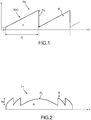
- the surface profile of these elements thus consists of continuous reliefs separated by discontinuities. These elements have a maximum efficiency for a determined wavelength ⁇ 0, called blaze wavelength.
- ⁇ ⁇ 0 2 ⁇
- n is the index of the material composing the network and h0 is the height of the echelette.
- Order 1 Light lost in the order of blaze (order 1) is diffracted in higher orders. If we take the example of a hybrid lens, which is composed of a refractive lens on one side and diffractive on the other side and where the role of the diffractive face is to correct the chromatic aberrations of the refractive lens, this phenomenon results in the transmission of a parasitic light, which is harmful to the quality of the imagery. This is conveniently reflected by the appearance of diffracted light throughout the image plane. For example, the output image is not clear, or is dull.
- the low dispersion of the optical material in conventional diffractive optical elements results in a drop in diffraction efficiency with the wavelength ⁇ ⁇ ⁇ 0 expressed by equation (1).
- This variation of the phase difference with the wavelength is also present for the diffractive components operating in reflection.
- binary microstructure also known as blazed binary gratings, or sub-wavelength diffractive optics (SWDOE), described in the publication
- SWDOE sub-wavelength diffractive optics
- These blazed binary networks are designed by performing a binary synthesis of the profile of a conventional diffractive optical element: we start from the conventional diffractive optical element that we want to synthesize and we sample this network to obtain points, to which we can associate a value of index or phase shift. Sampling must be done at a time less than the design wavelength to obtain a sub-wavelength network.
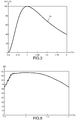
- a blazed binary network corresponding to the RE network of the figure 4a is represented on the figure 4b .
- the network RE is sampled on a number of points at the period ⁇ s chosen to be less than the blaze wavelength ⁇ 0 . A certain number of points are obtained for each period A of the network.
- the binary microstructures are of the pillar type.
- a set of binary microstructures is obtained which encodes the grating pattern. This set of microstructures is repeated at period A of the echelette grating of the figure 4a .
- a filling factor f is defined for each microstructure which varies from one microstructure to another to follow the phase function of the echelette grating.
- this dimension d increases with x.
- the filling factor f of a binary microstructure of the network can take any real value between 0 and 1, including the values 0 and 1. For example, for the pillar p 0 on the figure 4b , the fill factor is 0.
- n eff effective index n eff to describe the interaction of light on microstructures.
- the structure of the element is assimilated to a homogeneous artificial material, giving the component an index profile comparable to an effective index gradient network, whose effective index varies over the period A (or the portion) of the considered network.
- the figure 4c schematically represents an effective index gradient network corresponding to the binary blazed network of the figure 4b .
- the effective index is a function of the filling factor f (and thus the sampling period ⁇ s ), the geometry of the microstructure, the index n of the material (or, what is equivalent, its permittivity ⁇ ) and the incident wavelength ⁇ .
- Various analytical formulas are thus known to those skilled in the art, which make it possible to calculate, for a given artificial material, the curves of variation of the effective index as a function of the filling factor f of the microstructures (therefore as a function of d and ⁇ s ) and as a function of the incident wavelength ⁇ .
- the blaze effect ie the diffraction of the incident light in a single diffraction order, the blaze order
- the microstructures are too small (sub-wavelength) to be solved by the incident light (in terms of far-field diffraction) which perceives locally, a mean index, the effective index n eff .
- the use of sub- ⁇ microstructures makes it possible to achieve an optimized phase law so that the energy radiated in the main deflected beam (blaze order) is favored, and the diffracted energy in the parasitic diffracted beams is minimized.
- microstructures have geometries either hollow type hole, for example cylindrical, or protrusions type pillar, for example round, square, hexagonal or rectangular. A combination of holes and pillars is also possible.
- the microstructures are of any shape, preferably with axes of symmetry to make them independent of the polarization of the incident beam at normal incidence.
- ⁇ s are arranged, within a period (network) or a part (Fresnel lens), according to a sampling period ⁇ s at least on the direction 0x of the surface plane of the network or according to a radius starting from the center for a lens for a lens in the axis.
- the structure of an off-axis lens is also applicable to the invention.
- the figure 6 illustrates an element 60 synthesizing a network based P pillars seen from above.
- there is a microstructure P per mesh for example in the center of each mesh.
- the microstructures aligned along the 0X direction of the XY surface plane of the network are assigned a filling factor varying progressively in a determined order, increasing or decreasing along the main direction 0X of the network.
- the microstructures aligned according to the other dimension 0Y of the network have an identical filling factor.
- the filling factor of these microstructures can vary in all directions.
- blazed binary diffractive optical elements are known to have efficiencies far superior to those of conventional optics, and are used in the case of high dispersion networks or hybrid lenses with high numerical aperture.
- the document WO 2005/038501 also describes a particular type of transmission blazed network using the strong dispersion of the artificial materials to compensate for the variation of the diffraction efficiency as a function of the wavelength of the incident beam, in order to obtain elements of diffractive optics blazed over a broad spectral band, that is to say diffractive optics elements effective in their order of blaze over a wide spectral range.
- These particular networks, as illustrated figure 7 use two different microstructures, such as m1 holes and m2 pillars. In a first portion, the microstructures according to the first geometry have a decreasing effective index with the filling factor, and in a second portion the microstructures according to the second geometry synthesize an effective index increasing with the filling factor.
- Composite artificial material 70 whose structure is illustrated figure 7 has an effective index gradient that varies between a minimum value n eff / min and a maximum value n eff / max .
- the minimum and maximum effective indices of the material are determined from the curves of variation of the effective index with the filling factor of the microstructures.
- design wavelength or blaze wavelength
- ⁇ ⁇ long wavelength before design wavelength ⁇ 0 With ⁇ 0 design wavelength (or blaze wavelength) and ⁇ ⁇ long wavelength before design wavelength ⁇ 0 .
- the characterization parameter ⁇ must be strictly greater than 0, ⁇ > 0 and preferably 0.3 ⁇ ⁇ 0.5.
- the characteristics of the material 70 are thus determined so as to obtain extreme effective index values resulting in the value of ⁇ desired.
- the sampling period ⁇ s encodes the period area A equal to 25 ⁇ 0 , corresponding to 50 microstructures (35 holes and 15 pillars).
- the engraving depth h is 1.875 ⁇ 0 .
- ⁇ 0.39.
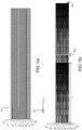
- the diffraction efficiency curve as a function of the wavelength is given to the figure 8 : we obtain an area around ⁇ 0 wide enough in which the diffraction efficiency is at its maximum equal to 96% and remains above 90% between 0.6 ⁇ 0 and 1.5 ⁇ 0 .
- the diffraction efficiency does not reach 100% in practice because of discontinuities in the surface profile when moving from one type of geometry to another. At the discontinuity level, there is a shading effect and a phase discontinuity effect.
- the diffraction efficiency of this grating was calculated for a grating period A equal to 25 ⁇ 0 .
- A the effect of the discontinuities is less, and the efficiency is therefore better.
- the effect of discontinuities is greater and efficiency is lost.
- a lower spectral width is obtained, but the improvement of the bandwidth may be satisfactory for some applications.
- composite artificial materials is not limited to components operating in the scalar domain.
- the concept of composite artificial material can be applied to the realization of different sub-wavelength diffractive components, such as an illustrated network. figure 9 or an illustrated Fresnel lens figure 10 .
- the spectral width of the diffraction efficiency shown on the figure 8 is not sufficient for certain applications such as spectroscopy and the realization of optical or radiofrequency instruments for space (telescopes ..).
- the parameter ⁇ depends significantly on the chosen material, the period and the height of the structures, this having to take into account the manufacturing constraints.
- the choice of material is not always favorable to a parameter ⁇ > 0.3, corresponding to a value conducive to use of the component over a very wide band. he It is therefore not always easy to find all the ideal conditions for the parameter ⁇ . It is often necessary to be satisfied with a slightly reduced ⁇ .
- An object of the present invention is to overcome the aforementioned drawbacks by proposing a sub-wavelength diffractive component having a spectral width of its enhanced diffraction efficiency and a greater flexibility of design to obtain an efficiency curve mask ⁇ ( ⁇ ) given.
- the elementary zones are joined.
- the surface is flat or curved.
- the incident beam is a light wave or radiofrequency.
- the elementary zones are arranged on a transparent substrate, the component being configured to diffract the beam by transmission.
- the component according to the invention further comprises a reflector, the reflector being disposed between the elementary zones and a substrate, the component being configured to diffract the beam by reflection.
- the component corresponds to a Fresnel lens having a central portion and a plurality of peripheral portions, in which each elementary zone of type i corresponds to at least one sector of a portion of the Fresnel lens.
- the component corresponds to a network, each elementary zone of type i corresponding to a blazed network at the blaze length ⁇ i of index i, each elementary zone having a periodic effective variation of inde in a period axis X identical for all types, a dimension of an elementary zone in the direction X being equal to a multiple of the period.
- the dimension of an elementary zone along X corresponds to the dimension of the component according to X.
- the elementary zones are arranged in a direction Y perpendicular to X so that all the types follow each other once, a plurality of times, and in which the order of the types and the dimension according to Y of the zones of each type is repeated identically.
- the microstructures of an elementary zone have a pillar shape, a hole shape or a combination of both.
- the diffractive component according to the invention further comprises an antireflection layer disposed over the microstructures.
- the antireflection layer is a structured layer at the subwavelength scale.
- the component according to the invention further comprises a plurality of secondary microstructures having a size smaller than the size of the basic microstructures.
- the microstructures are arranged so that the difference ⁇ n eff (i) satisfies the blaze condition for a value of height h that is identical for all types.
- the figure 11 illustrates a broadband diffractive component according to the invention, of network type 10.
- the description of the diffractive component is made below for the illustrated network component figure 11 (11a, 11b and 11c) but the developed considerations apply in the same way to a broadband diffractive component according to the invention of the Fresnel lens type illustrated.
- Figure 12 (12a, 12b and 12c) .
- the diffractive component (20) according to the invention is able to diffract an incident beam, which is typically a light beam, for example visible / infrared or a microwave beam, typically between 300 MHz and 300 GHz (see for example the document WO2014 / 128015 ), having a wavelength in a BSD diffraction spectral band.
- an incident beam which is typically a light beam, for example visible / infrared or a microwave beam, typically between 300 MHz and 300 GHz (see for example the document WO2014 / 128015 ), having a wavelength in a BSD diffraction spectral band.
- the diffractive component whose top view is illustrated figure 11a (network) and figure 12a (Fresnel lens) comprises a plurality of elementary zones Z1, Z'1, Z "1, Z2, Z'2, Z" 2, Z3, Z'3, Z "3, Z4, Z'4 .... arranged on a surface S.
- Each elementary zone belongs to a type indexed by an index i comprised between 1 and n with n (integer) strictly greater than 1, the index i corresponding to a blaze wavelength ⁇ i of index
- the diffractive component according to the invention comprises at least two elementary zones of different type.
- the zones Z1, Z'1, Z "1 are of type 1, ie they correspond to a blaze length ⁇ 1
- the zones Z2, Z'2, Z" 2 are of type 2, it is to say correspond to a blaze length ⁇ 2, etc ...
- the blaze wavelengths ⁇ 1, ⁇ 2, ⁇ i, ⁇ N are included in the diffraction spectral band BSD of the diffractive component (20).
- An elementary zone of type i Zi, Z'i, Z "i comprises a plurality of microstructures MSi having respectively at least a size di of less than 1.5 times the blaze wavelength ⁇ i of index i so that the component operates globally under subwavelength regime.
- all the microstructures of an elementary zone have a size di of less than 1.5 times the blaze wavelength ⁇ i of index i.
- the size of the microstructures is thus globally of the order of magnitude or less than the blaze wavelength.
- all the microstructures of an elementary zone have a size di less than 1.2 times the blaze wavelength ⁇ i of index i to prevent a loss of efficiency by diffraction on the parasitic orders.
- microstructures are arranged to form an artificial material having an effective index variation n eff (i) so that the elementary zone type i constitutes a diffractive element blazed to the blaze length ⁇ i of index i.
- each elementary zone of type i is a zone having a subwavelength structure corresponding to a structure described in the state of the art, for a design wavelength (or blaze) equal to ⁇ i.
- Microstructures are pillars, holes, or a combination of both.
- the respective shape of the holes or pillars may vary (rectangular, hexagonal, circular section), and during a transition pillars / holes within the same period, a particular form of hole or pillar can be used.
- Figures 11b and 12b represent zones of type i consisting of pillars MSi of size di and height hi variable, and Figures 11c and 12c represent the corresponding effective index variation.
- Zone Z1 of the figure 11 b corresponds to a blazed network and therefore has a periodic structure of period ⁇ according to at least one dimension X.
- Zones Z'1, Z "'1 (type 1) of the figure 12b correspond to sectors of the central portion Pc of a Fresnel lens
- zones Z """'2 (type 2) and Z"' 4 (type 4) correspond to sectors of the peripheral part corresponding to the first ring .
- zones of type 1 Z1, Z'1, Z "1, ...), of type 2 (Z2, Z'2, ...) etc ... are distributed according to the surface S.
- the zones are distributed in any way, in no particular order.
- each type zone i (Zi, Z'i, Z "i, ...) diffracting around a given blaze length contributes to the overall diffraction efficiency of the component, which benefits from a resulting effect.
- the proportion of area occupied by all the zones of a given type makes it possible to adapt to a template of the desired overall diffraction efficiency.
- the percentage of surface associated with a type makes it possible to introduce a weighting of the contribution of the different blaze wavelengths into the overall diffraction efficiency.
- the existence of a plurality of blaze wavelengths allows the diffractive component (for example a Fresnel lattice or lens) according to the invention, which we will call a binary multi-blaze diffractive component (binary means that it is based on microstructures), to exhibit better broadband behavior than a blazed component at a single wavelength as illustrated figures 3 or 8 .
- the weighting by the surface gives a great flexibility of design to obtain the desired efficiency. Illustrations of this property are given below.
- the invention makes it possible to dispense with the condition at ⁇ for example or to allow a reduction of the parameter ⁇ while maintaining a good spectral efficiency.
- the broadband behavior is obtained thanks to a design making it possible to obtain a value of the parameter ⁇ which is large enough (of the order of 0.3).
- the authors have made a judicious choice over the sampling period, the material and the choice of sizes and geometries of structures to obtain the desired parameter ⁇ .
- the choice of materials is not always possible.
- the use of a material with a low refractive index inevitably leads to a lower dispersion of its effective index. The consequence is a limitation of its broadband effect.
- a binary multiblaze component makes it possible to reduce the design constraints weighing on each zone, thus allowing more degrees of freedom. It may, for example, combine several zones, some zones being designed with a reduced parameter ⁇ and others with a larger parameter ⁇ , without reducing the spectral band of use.
- the technology for producing sub-wavelength diffractive components is particularly suitable for manufacturing these components, impossible to achieve with traditional structures ladders. It is completely compatible in the realization of components combining different areas in the x direction and / or in the y direction.
- each elemental zone of type i corresponds to at least one sector of a portion of the Fresnel lens.
- the sector of a given type corresponds to the whole of the part, that is to say that each part (Pa, a) constitutes a zone of a certain type, for example the the whole of the central zone is of type 1 (blazed at ⁇ 1), the first ring is of a second type (blazed at ⁇ 2), the third ring is of a third type or the first type or the second type.
- the central portion Pc and each peripheral ring have several sectors, the sectors being of different types.
- each elementary zone of type i corresponds to a blazed network with the blaze length ⁇ i of index i, and therefore each elementary zone has an effective index variation n eff (i) periodic along an axis X of identical period ⁇ .
- n eff (i) periodic along an axis X of identical period ⁇ .
- the elementary zones are contiguous.
- the surface S on which the microstructures of the diffractive component 10 or 20 according to the invention are arranged is flat or curved, and the incident beam diffracted by the component is a light wave (typically visible and / or infrared) or radiofrequency .
- a light wave typically visible and / or infrared
- radiofrequency typically visible and / or infrared
- technologies such as the nanoimprint for defining patterns of structures on a spherical surface, for example from a flexible buffer, are particularly well suited.
- the pad being made for example by lithography and etching.
- the elementary zones are made of a transparent material and arranged on a substrate that is also transparent, for example silica.
- a multiblaze binary component according to the invention configured to diffract an incident beam Fi according to a reflection diffracted beam Fd further comprises a surface or a reflective element R.
- the reflector R is disposed between the elementary zones Zi and a substrate S.
- the elementary zones are in this case made of a transparent material, but the substrate S may not be transparent.
- the advantage of using a mirror below is to be able to use the dispersion of the effective index of subwavelength structures, with a dielectric structure that synthesizes the phase function.
- a structured metal or a metal above a layer structured at the sub-wavelength scale it is possible to encounter extraordinary resonance or transmission phenomena which cause a strong drop of diffraction efficiency in reflection.
- the reflector consists of a metal layer or a multi-layer dielectric assembly.
- broadband reflective networks are used, and for imaging applications, for concentration functions, or for hyper-beam processing, Fresnel lenses operating in transmissive mode are used for 'to integrate easily in existing systems (hybrid systems mixing conventional optics and diffractive optics). But we can also find networks in transmission and lenses in reflection.
- microstructures MSi of a zone of type i have a height hi indexed i.
- the condition of blaze is expressed by a relation connecting the quantities ⁇ n eff (i), hi and ⁇ i. It corresponds to an effective index variation and a height calculated to induce a 2 ⁇ phase variation between the incident beam and the diffracted beam.
- phase law and thus the effective index variation, over a period (network) or part (central or peripheral of a lens) is almost monotonous.
- the phase law, and thus the effective index variation, over a period or part is constant by subintervals, that is to say variable in steps.
- the following considerations are given for a period of a network but are also applicable to each part (center and rings) of a Fresnel lens.
- the period ⁇ of the network is sampled according to a sampling period ⁇ sx less than ⁇ dividing the period ⁇ and defining sampling intervals.
- the sampling period is different for each type, but advantageously the sampling period according to X, ⁇ sx, is the same for all types (direction of variation of the effective index).
- the sampling period according to Y, ⁇ sy is the same for all types.
- the sampling period according to X and Y is identical (square mesh).
- the microstructures are arranged within each sampling interval so as to correspond to a given value of effective index in the interval.
- the index variation effectiff n eff according to the period ⁇ is thus sampled according to a period ⁇ s.
- the phase law synthesized with the microstructures makes it possible to produce a discontinuous phase law in steps or jumps, each jump corresponding to a given value of phase and therefore to a given value of effective index.
- the law of variation of the phase between 0 and 2 ⁇ induced by the variation of the effective index is not necessarily linear (in stages or not), it can be non-linear, or locally non-monotonic.
- microstructures shape, filling ratio, height
- a broadening of the intrinsic spectral band of an element blazed at ⁇ i is also obtained for microstructures synthesizing an effective index variation having a coefficient ⁇ i strictly positive.
- the microstructures of the elementary zones are arranged so that the difference ⁇ n eff (i) satisfies the blaze condition for a value of height h that is identical for all the types present in the component.
- the dimension LX of an elementary zone according to X corresponds to the dimension of the component according to X, as illustrated figure 14 .
- all the elementary zones Zi, Z'i ... have the same dimension according to X whatever their type.
- the microstructures can be arranged in different ways known from the state of the art.
- the microstructures have a hexagonal, circular or square section.
- the microstructures have a plurality of variable sizes along a direction having an effective index variation. And advantageously a microstructure at most is arranged by sampling interval.
- the microstructures have a given principal size di0 (by type) and a density per unit of variable area along a direction having an effective index variation.
- di0 is identical regardless of i and equal to d0.
- the elementary zones are arranged in a direction Y perpendicular to X so that all the types succeed one another each a plurality of times.
- the component binary multiblaze comprises zones of three different types
- the zones according to Y succeed one another Z1, Z2, Z3, then again three zones each of a different type Z'2, Z'1, Z'3, ... and so right now.
- the dimensions along Y of the different zones are different, but advantageously the succession of types and the dimension according to Y of the zones of each type is repeated identically. This simplifies the elementary mask used for the manufacture of the multiblaze binary network.
- the figure 15 illustrates an example of such a network.
- the sampling periods ⁇ sx and ⁇ sy are identical, and each zone has a dimension according to Y equal to a sampling period ⁇ sy according to Y.
- the areas include holes and / or pillars.
- the black color corresponds to a dielectric material such as silica, and white to air.
- Area 1 blazed at 850 nm comprises 6 pillars and 40 holes, and zone 2 blazed at 500 nm comprises 46 holes.
- the period ⁇ is 16 ⁇ m and the height h is 1.5 ⁇ m.
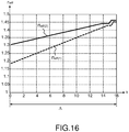
- the figure 16 illustrates the change in effective index over a period obtained for the two lengths of blaze.
- the solid curve corresponds to the type 2 zone blazed at 500 nm and the dotted curve corresponds to the type 1 zone blazed at 850 nm.
- the index variation is linear and smoothed from the value obtained for each mesh.
- Oscillations of large amplitudes of the efficiency at long wavelengths are due to a Fabry Perot effect specific to the reflective mode.
- the diffractive component according to the invention further comprises an antireflection layer AR, preferably disposed over the microstructures, as illustrated. figure 19 .
- AR antireflection layer
- the antireflection layer may be deposited for example by PVD for "Physical Vapor Deposition” such as evaporation or sputtering or by CVD for "Chemical Vapor Deposition” such as ALD “Atomic Layer Deposition” or PECVD “Plasma Enhanced Chemical Vapor Deposition "
- the air between the microstructures (pillars) or in them (holes) is replaced by a material. This adds a degree of freedom to the design of the structure, and the presence of this material facilitates the deposition of the AR layer if necessary.
- the AR antireflection layer is a subwavelength structured layer, as illustrated figure 19a .
- the figure 19bisa illustrates the structure of the component according to the invention seen in profile
- the figure 19bisb illustrates the antireflection layer AR seen from above
- the figure 19bisc illustrates an example of zones according to the invention seen from above.
- the structuring of the antireflection layer consists, for example, in the production of holes therein, preferably passing through as illustrated. figure 19a , which decreases the effective index of the AR layer.
- the AR layer is then a better anti-reflection for microstructures made with a low index material.
- a variant of this preferred embodiment consists in adding a plurality of secondary microstructures MSsi to the basic microstructures MSi, the secondary microstructures having a size smaller than the size of the basic microstructures.
- These secondary microstructures are technologically feasible when the initial microstructures have appropriate sizes for the diffraction of microwave waves, that is to say typically sizes of the order of mm or cm (see document WO2014 / 128015 figures 8 and 9 and corresponding description). They allow a finer adjustment of the value of the effective index and realize an impedance matching layer (anti-reflection).
- the Figures 20 and 21 illustrate two examples of network 10 according to the invention operating in reflective mode as illustrated figure 13 , consisting of two types of zones, type 1 corresponding to a blaze at 850 nm and type 2 to a blaze at 500 nm.
- the black color corresponds to the material and the white color to the air.
- the period ⁇ is 2.45 ⁇ m and a period according to X consists of 7 holes of height 1.7 ⁇ m whose respective size is determined so as to obtain the desired blaze.
- the network of figure 20 consists of alternating zones of types 1 and 2, each zone corresponding to once the sampling period according to Y.
- the proportion of surface of each type is 50%, each type therefore has an identical weight.
- the network of figure 21 consists of an alternation of a type 1 zone having a dimension according to Y corresponding to one sampling period according to Y, and a zone of type 2 having a dimension according to Y corresponding to twice the period of
- the proportion of surface area of the component with a type 1 blazed network is therefore 33% and the surface proportion for type 2 is 67%, therefore a higher weight is given to type 2 (blaze at 500 nm).
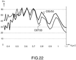
- the figure 22 illustrates the calculated diffraction efficiency curves of the two examples described above, the curve C50 / 50 corresponding to the network of the figure 20 and curve C67 / 33 corresponding to the network of the figure 21 .
- the two curves exhibit a very wide band diffraction efficiency between 0.35 and 1.1 ⁇ m. It is also noted that the curve C67 / 33 which corresponds to a network giving more weight to the type 2 has an overall efficiency higher than the visible wavelengths and lower than the wavelengths IR, compared to the network giving a weight equivalent to two types.
- the respective weight of the different types allows great flexibility in the design of the diffractive component, and allows to choose the desired spectral performance of the component by releasing the constraints on areas of a given type.
- optical system It is also possible in an optical system to combine several types of detectors sensitive to spectral ranges of different wavelengths.
Landscapes
- Physics & Mathematics (AREA)
- General Physics & Mathematics (AREA)
- Optics & Photonics (AREA)
- Engineering & Computer Science (AREA)
- Mathematical Physics (AREA)
- Theoretical Computer Science (AREA)
- Diffracting Gratings Or Hologram Optical Elements (AREA)
Applications Claiming Priority (1)
| Application Number | Priority Date | Filing Date | Title |
|---|---|---|---|
| FR1600237A FR3047810B1 (fr) | 2016-02-12 | 2016-02-12 | Composant diffractif sub longueur d'onde large bande spectracle |
Publications (1)
| Publication Number | Publication Date |
|---|---|
| EP3206059A1 true EP3206059A1 (de) | 2017-08-16 |
Family
ID=56101524
Family Applications (1)
| Application Number | Title | Priority Date | Filing Date |
|---|---|---|---|
| EP17153295.5A Pending EP3206059A1 (de) | 2016-02-12 | 2017-01-26 | Beugungskomponente unter spektral breitbandiger wellenlänge |
Country Status (3)
| Country | Link |
|---|---|
| US (1) | US10175496B2 (de) |
| EP (1) | EP3206059A1 (de) |
| FR (1) | FR3047810B1 (de) |
Cited By (2)
| Publication number | Priority date | Publication date | Assignee | Title |
|---|---|---|---|---|
| WO2021079077A1 (fr) | 2019-10-24 | 2021-04-29 | Hydromecanique Et Frottement | Dispositif optique |
| CN118210092A (zh) * | 2024-05-22 | 2024-06-18 | 苏州大学 | 一种宽波段复合超表面光栅及其设计方法 |
Families Citing this family (10)
| Publication number | Priority date | Publication date | Assignee | Title |
|---|---|---|---|---|
| US10712475B2 (en) | 2017-08-16 | 2020-07-14 | Lumentum Operations Llc | Multi-layer thin film stack for diffractive optical elements |
| US10802185B2 (en) | 2017-08-16 | 2020-10-13 | Lumentum Operations Llc | Multi-level diffractive optical element thin film coating |
| US11016227B2 (en) | 2017-09-18 | 2021-05-25 | Lumentum Operations Llc | Diffractive optical element |
| JP7226915B2 (ja) * | 2017-12-26 | 2023-02-21 | デクセリアルズ株式会社 | 凹凸構造体、光学部材及び電子機器 |
| WO2020092529A1 (en) * | 2018-10-30 | 2020-05-07 | Arizona Board Of Regents On Behalf Of The University Of Arizona | An ultralight very large aperature space telescopes and methods using mode lens and shims |
| US11538273B2 (en) * | 2018-12-03 | 2022-12-27 | Beijing Boe Technology Development Co., Ltd. | Integrated photo-sensing detection display apparatus and method of fabricating integrated photo-sensing detection display apparatus |
| CN109643380B (zh) * | 2018-12-03 | 2023-04-18 | 京东方科技集团股份有限公司 | 集成光感检测显示设备及其制造方法 |
| CN109856718B (zh) * | 2018-12-31 | 2023-11-10 | 苏州大学 | 低偏振度二维二元闪耀光栅 |
| CN109887944B (zh) * | 2019-03-05 | 2022-04-05 | 西安工业大学 | 具有多功能窗口的全天时成像探测器及其制备方法 |
| WO2024180785A1 (ja) * | 2023-03-01 | 2024-09-06 | ソニーグループ株式会社 | 光学素子 |
Citations (3)
| Publication number | Priority date | Publication date | Assignee | Title |
|---|---|---|---|---|
| WO2005038501A1 (fr) | 2003-10-15 | 2005-04-28 | Thales | Elements d’optique diffractive de type binaire pour une utilisation en large bande spectrale |
| US20130076581A1 (en) * | 2011-09-26 | 2013-03-28 | Thales | Antenna lens comprising a dielectric component diffractive suitable shaping a wavefront microwave |
| WO2014128015A1 (fr) | 2013-02-22 | 2014-08-28 | Thales | Systeme de deflexion configurable hyperfrequence |
Family Cites Families (4)
| Publication number | Priority date | Publication date | Assignee | Title |
|---|---|---|---|---|
| JP2001290074A (ja) * | 2000-04-04 | 2001-10-19 | Canon Inc | 回折光学素子を有する光学系 |
| JP3837089B2 (ja) * | 2002-06-07 | 2006-10-25 | 松下電器産業株式会社 | 回折素子および光ピックアップヘッド装置 |
| AU2003267004A1 (en) * | 2002-08-24 | 2004-04-30 | Carl Zeiss Smt Ag | Binary blazed diffractive optical element |
| DE10322239B4 (de) * | 2003-05-17 | 2011-06-30 | Carl Zeiss SMT GmbH, 73447 | Geblazetes diffraktives optisches Element sowie Projektionsobjektiv mit einem solchen Element |
-
2016
- 2016-02-12 FR FR1600237A patent/FR3047810B1/fr active Active
-
2017
- 2017-01-26 EP EP17153295.5A patent/EP3206059A1/de active Pending
- 2017-02-08 US US15/428,093 patent/US10175496B2/en active Active
Patent Citations (5)
| Publication number | Priority date | Publication date | Assignee | Title |
|---|---|---|---|---|
| WO2005038501A1 (fr) | 2003-10-15 | 2005-04-28 | Thales | Elements d’optique diffractive de type binaire pour une utilisation en large bande spectrale |
| US20070103782A1 (en) * | 2003-10-15 | 2007-05-10 | Lee Mane-Si L | Binary type diffractive optical elements for wide spectral band use |
| US20130076581A1 (en) * | 2011-09-26 | 2013-03-28 | Thales | Antenna lens comprising a dielectric component diffractive suitable shaping a wavefront microwave |
| WO2014128015A1 (fr) | 2013-02-22 | 2014-08-28 | Thales | Systeme de deflexion configurable hyperfrequence |
| US20150380829A1 (en) * | 2013-02-22 | 2015-12-31 | Thales | Configurable microwave deflection system |
Non-Patent Citations (3)
| Title |
|---|
| "SubWavelength Diffractive Optic Element), décrits dans la publication « Broadband blazing with artificial dieclectrics", OPTICS LETTERS, vol. 29, no. 14, 2004 |
| PH. LALANNE; D. LEMERCIER-LALANNE: "On the effective medium theory of subwavelength periodic structures", JOURNAL OF MODERN OPTICS, vol. 43, no. 10, 1996, pages 2063 - 2085, XP009178416, DOI: doi:10.1080/09500349608232871 |
| PH.LALANNE: "Waveguiding in blazed-binary diffractive elements", JOURNAL OF OPT. SOC. AM. A., vol. 16, 1999, pages 2517 - 2520 |
Cited By (7)
| Publication number | Priority date | Publication date | Assignee | Title |
|---|---|---|---|---|
| WO2021079077A1 (fr) | 2019-10-24 | 2021-04-29 | Hydromecanique Et Frottement | Dispositif optique |
| WO2021079078A1 (fr) | 2019-10-24 | 2021-04-29 | Hydromecanique Et Frottement | Dispositif optique |
| FR3102574A1 (fr) | 2019-10-24 | 2021-04-30 | Hydromecanique Et Frottement | Dispositif optique adapté à la transmission/réflexion d'un rayonnement électromagnétique |
| FR3102565A1 (fr) | 2019-10-24 | 2021-04-30 | H.E.F. | Dispositif optique avec une texturation de surface |
| US12287453B2 (en) | 2019-10-24 | 2025-04-29 | Hydromecanique Et Frottement | Multilayer optical device with surface texturing and extended cavities for electromagnetic radiation |
| US12392934B2 (en) | 2019-10-24 | 2025-08-19 | Hydromecanique Et Frottement | Optical device with surface texturing extending through coating layer into substrate |
| CN118210092A (zh) * | 2024-05-22 | 2024-06-18 | 苏州大学 | 一种宽波段复合超表面光栅及其设计方法 |
Also Published As
| Publication number | Publication date |
|---|---|
| US20170235153A1 (en) | 2017-08-17 |
| US10175496B2 (en) | 2019-01-08 |
| FR3047810A1 (fr) | 2017-08-18 |
| FR3047810B1 (fr) | 2018-05-25 |
Similar Documents
| Publication | Publication Date | Title |
|---|---|---|
| FR3047810A1 (fr) | Composant diffractif sub longueur d'onde large bande spectracle | |
| EP1678531B1 (de) | Beugendes binäres optisches element zur verwendung in einem grossen spektralen bereich | |
| EP3568719B1 (de) | Linse mit fokussierender meta-oberfläche und geringer chromatischer aberration | |
| EP2559069B1 (de) | Optischer mono- oder mehrfrequenzfilter und detektor mit einem derartigen filter | |
| EP2616855B1 (de) | Spektralbandpassfilter mit hoher selektivität und gesteuerter polarisation | |
| EP3607585B1 (de) | Vorrichtung und verfahren zur multispektralen bildgebung im infrarotbereich | |
| EP2573872A1 (de) | Linsenantenne, die eine dielektrische, beugende Komponente umfasst, die in der Lage ist, eine Hyperfrequenzwellenfront zu formen | |
| EP2926187B1 (de) | Vorrichtung zur steuerung der phase einer lichtwellenfront | |
| WO2011073554A1 (fr) | Réseau de diffraction réfléchissant diélectrique optimisé | |
| EP0102272B1 (de) | Verfahren zur Fokussierung von holographischen sphärischen Beugungsrastern, die in der Reflektion arbeiten; streuende Objektive und Spektrometer unter Anwendung desselben | |
| EP1974194A1 (de) | Farbloses und kompaktes optisches dreiseitiges verschiebungsinterferometer | |
| EP1700141B8 (de) | Zweidimensionales beugungsgitter mit alternierenden mehrschichtstapeln und spektroskopische einrichtung mit dem gitter | |
| EP1061349A1 (de) | Achromatisches optisches Interferometer mit kontinuierlich einstellbarer Empfindlichkeit | |
| WO2009053422A1 (fr) | Dispositif d'imagerie a codage de pupille sub-longueur d'onde | |
| FR2723216A1 (fr) | Optique diffractive en infrarouge applicable a un systeme de designaton d'objectif par laser | |
| WO2015158882A2 (fr) | Filtre en transmission selectif en longue d'onde a cavite resonnante | |
| WO2020002330A1 (fr) | Filtre spectral comprenant au moins deux structures de fabry-perot couplees | |
| WO2019197754A1 (fr) | Filtrage spectral de rayonnement électromagnétique | |
| WO2024052607A1 (fr) | Filtre spectral a resonateurs couples | |
| WO2016001326A1 (fr) | Détecteur propre à détecter une première longueur d'onde et à filtrer une deuxième longueur d'onde | |
| FR3031400A1 (fr) | Dispositif optique de focalisation | |
| WO2010069836A1 (fr) | Dispositif de spectrometrie compact et procede de fabrication |
Legal Events
| Date | Code | Title | Description |
|---|---|---|---|
| PUAI | Public reference made under article 153(3) epc to a published international application that has entered the european phase |
Free format text: ORIGINAL CODE: 0009012 |
|
| STAA | Information on the status of an ep patent application or granted ep patent |
Free format text: STATUS: THE APPLICATION HAS BEEN PUBLISHED |
|
| AK | Designated contracting states |
Kind code of ref document: A1 Designated state(s): AL AT BE BG CH CY CZ DE DK EE ES FI FR GB GR HR HU IE IS IT LI LT LU LV MC MK MT NL NO PL PT RO RS SE SI SK SM TR |
|
| AX | Request for extension of the european patent |
Extension state: BA ME |
|
| STAA | Information on the status of an ep patent application or granted ep patent |
Free format text: STATUS: REQUEST FOR EXAMINATION WAS MADE |
|
| 17P | Request for examination filed |
Effective date: 20171129 |
|
| RBV | Designated contracting states (corrected) |
Designated state(s): AL AT BE BG CH CY CZ DE DK EE ES FI FR GB GR HR HU IE IS IT LI LT LU LV MC MK MT NL NO PL PT RO RS SE SI SK SM TR |
|
| STAA | Information on the status of an ep patent application or granted ep patent |
Free format text: STATUS: EXAMINATION IS IN PROGRESS |
|
| 17Q | First examination report despatched |
Effective date: 20201211 |