EP3206239B1 - Puce semi-conductrice émettant un rayonnement - Google Patents
Puce semi-conductrice émettant un rayonnement Download PDFInfo
- Publication number
- EP3206239B1 EP3206239B1 EP17157898.2A EP17157898A EP3206239B1 EP 3206239 B1 EP3206239 B1 EP 3206239B1 EP 17157898 A EP17157898 A EP 17157898A EP 3206239 B1 EP3206239 B1 EP 3206239B1
- Authority
- EP
- European Patent Office
- Prior art keywords
- semiconductor chip
- layer
- radiation
- structural elements
- structured
- Prior art date
- Legal status (The legal status is an assumption and is not a legal conclusion. Google has not performed a legal analysis and makes no representation as to the accuracy of the status listed.)
- Active
Links
Images



Classifications
-
- H—ELECTRICITY
- H10—SEMICONDUCTOR DEVICES; ELECTRIC SOLID-STATE DEVICES NOT OTHERWISE PROVIDED FOR
- H10H—INORGANIC LIGHT-EMITTING SEMICONDUCTOR DEVICES HAVING POTENTIAL BARRIERS
- H10H20/00—Individual inorganic light-emitting semiconductor devices having potential barriers, e.g. light-emitting diodes [LED]
- H10H20/80—Constructional details
- H10H20/84—Coatings, e.g. passivation layers or antireflective coatings
-
- H—ELECTRICITY
- H01—ELECTRIC ELEMENTS
- H01S—DEVICES USING THE PROCESS OF LIGHT AMPLIFICATION BY STIMULATED EMISSION OF RADIATION [LASER] TO AMPLIFY OR GENERATE LIGHT; DEVICES USING STIMULATED EMISSION OF ELECTROMAGNETIC RADIATION IN WAVE RANGES OTHER THAN OPTICAL
- H01S5/00—Semiconductor lasers
- H01S5/20—Structure or shape of the semiconductor body to guide the optical wave ; Confining structures perpendicular to the optical axis, e.g. index or gain guiding, stripe geometry, broad area lasers, gain tailoring, transverse or lateral reflectors, special cladding structures, MQW barrier reflection layers
- H01S5/22—Structure or shape of the semiconductor body to guide the optical wave ; Confining structures perpendicular to the optical axis, e.g. index or gain guiding, stripe geometry, broad area lasers, gain tailoring, transverse or lateral reflectors, special cladding structures, MQW barrier reflection layers having a ridge or stripe structure
-
- H—ELECTRICITY
- H01—ELECTRIC ELEMENTS
- H01S—DEVICES USING THE PROCESS OF LIGHT AMPLIFICATION BY STIMULATED EMISSION OF RADIATION [LASER] TO AMPLIFY OR GENERATE LIGHT; DEVICES USING STIMULATED EMISSION OF ELECTROMAGNETIC RADIATION IN WAVE RANGES OTHER THAN OPTICAL
- H01S5/00—Semiconductor lasers
- H01S5/20—Structure or shape of the semiconductor body to guide the optical wave ; Confining structures perpendicular to the optical axis, e.g. index or gain guiding, stripe geometry, broad area lasers, gain tailoring, transverse or lateral reflectors, special cladding structures, MQW barrier reflection layers
- H01S5/2004—Confining in the direction perpendicular to the layer structure
- H01S5/2018—Optical confinement, e.g. absorbing-, reflecting- or waveguide-layers
- H01S5/2022—Absorbing region or layer parallel to the active layer, e.g. to influence transverse modes
-
- H—ELECTRICITY
- H01—ELECTRIC ELEMENTS
- H01S—DEVICES USING THE PROCESS OF LIGHT AMPLIFICATION BY STIMULATED EMISSION OF RADIATION [LASER] TO AMPLIFY OR GENERATE LIGHT; DEVICES USING STIMULATED EMISSION OF ELECTROMAGNETIC RADIATION IN WAVE RANGES OTHER THAN OPTICAL
- H01S5/00—Semiconductor lasers
- H01S5/20—Structure or shape of the semiconductor body to guide the optical wave ; Confining structures perpendicular to the optical axis, e.g. index or gain guiding, stripe geometry, broad area lasers, gain tailoring, transverse or lateral reflectors, special cladding structures, MQW barrier reflection layers
- H01S5/22—Structure or shape of the semiconductor body to guide the optical wave ; Confining structures perpendicular to the optical axis, e.g. index or gain guiding, stripe geometry, broad area lasers, gain tailoring, transverse or lateral reflectors, special cladding structures, MQW barrier reflection layers having a ridge or stripe structure
- H01S5/2205—Structure or shape of the semiconductor body to guide the optical wave ; Confining structures perpendicular to the optical axis, e.g. index or gain guiding, stripe geometry, broad area lasers, gain tailoring, transverse or lateral reflectors, special cladding structures, MQW barrier reflection layers having a ridge or stripe structure comprising special burying or current confinement layers
-
- H—ELECTRICITY
- H01—ELECTRIC ELEMENTS
- H01S—DEVICES USING THE PROCESS OF LIGHT AMPLIFICATION BY STIMULATED EMISSION OF RADIATION [LASER] TO AMPLIFY OR GENERATE LIGHT; DEVICES USING STIMULATED EMISSION OF ELECTROMAGNETIC RADIATION IN WAVE RANGES OTHER THAN OPTICAL
- H01S5/00—Semiconductor lasers
- H01S5/20—Structure or shape of the semiconductor body to guide the optical wave ; Confining structures perpendicular to the optical axis, e.g. index or gain guiding, stripe geometry, broad area lasers, gain tailoring, transverse or lateral reflectors, special cladding structures, MQW barrier reflection layers
- H01S5/22—Structure or shape of the semiconductor body to guide the optical wave ; Confining structures perpendicular to the optical axis, e.g. index or gain guiding, stripe geometry, broad area lasers, gain tailoring, transverse or lateral reflectors, special cladding structures, MQW barrier reflection layers having a ridge or stripe structure
- H01S5/2205—Structure or shape of the semiconductor body to guide the optical wave ; Confining structures perpendicular to the optical axis, e.g. index or gain guiding, stripe geometry, broad area lasers, gain tailoring, transverse or lateral reflectors, special cladding structures, MQW barrier reflection layers having a ridge or stripe structure comprising special burying or current confinement layers
- H01S5/2218—Structure or shape of the semiconductor body to guide the optical wave ; Confining structures perpendicular to the optical axis, e.g. index or gain guiding, stripe geometry, broad area lasers, gain tailoring, transverse or lateral reflectors, special cladding structures, MQW barrier reflection layers having a ridge or stripe structure comprising special burying or current confinement layers having special optical properties
-
- H—ELECTRICITY
- H01—ELECTRIC ELEMENTS
- H01S—DEVICES USING THE PROCESS OF LIGHT AMPLIFICATION BY STIMULATED EMISSION OF RADIATION [LASER] TO AMPLIFY OR GENERATE LIGHT; DEVICES USING STIMULATED EMISSION OF ELECTROMAGNETIC RADIATION IN WAVE RANGES OTHER THAN OPTICAL
- H01S5/00—Semiconductor lasers
- H01S5/20—Structure or shape of the semiconductor body to guide the optical wave ; Confining structures perpendicular to the optical axis, e.g. index or gain guiding, stripe geometry, broad area lasers, gain tailoring, transverse or lateral reflectors, special cladding structures, MQW barrier reflection layers
- H01S5/22—Structure or shape of the semiconductor body to guide the optical wave ; Confining structures perpendicular to the optical axis, e.g. index or gain guiding, stripe geometry, broad area lasers, gain tailoring, transverse or lateral reflectors, special cladding structures, MQW barrier reflection layers having a ridge or stripe structure
- H01S5/2205—Structure or shape of the semiconductor body to guide the optical wave ; Confining structures perpendicular to the optical axis, e.g. index or gain guiding, stripe geometry, broad area lasers, gain tailoring, transverse or lateral reflectors, special cladding structures, MQW barrier reflection layers having a ridge or stripe structure comprising special burying or current confinement layers
- H01S5/2218—Structure or shape of the semiconductor body to guide the optical wave ; Confining structures perpendicular to the optical axis, e.g. index or gain guiding, stripe geometry, broad area lasers, gain tailoring, transverse or lateral reflectors, special cladding structures, MQW barrier reflection layers having a ridge or stripe structure comprising special burying or current confinement layers having special optical properties
- H01S5/222—Structure or shape of the semiconductor body to guide the optical wave ; Confining structures perpendicular to the optical axis, e.g. index or gain guiding, stripe geometry, broad area lasers, gain tailoring, transverse or lateral reflectors, special cladding structures, MQW barrier reflection layers having a ridge or stripe structure comprising special burying or current confinement layers having special optical properties having a refractive index lower than that of the cladding layers or outer guiding layers
Definitions
- the invention relates to a radiation-emitting semiconductor chip and a method for its production.
- the DE 10 2006 017 573 A1 discloses an optoelectronic semiconductor body.
- Windisch R. et al., IEEE Transactions on Electron Devices, Vol. 47, No. 7, July 2000, pp. 1492-1498 discloses a radiation emitting semiconductor chip with thin film surface texture.
- US 2006/0193353 A1 discloses a high power single mode semiconductor laser and US Pat EP 1012933 B1 discloses a laser device.
- Radiation-generating semiconductor chips typically contain semiconductor materials whose refractive index is relatively high compared to a surrounding medium, for example air. The consequence of this is that when radiation is coupled out at an interface between the semiconductor chip and the surrounding medium, total reflections can easily occur, which leads to a reduced light yield.
- an object to be achieved consists in specifying a manufacturing method for such a radiation-emitting semiconductor chip. This object is achieved by a method according to patent claims 10 or 11.
- the present invention is based, inter alia, on the idea of adjusting a refractive index transition that occurs between a first medium with a first refractive index and a second medium with a second refractive index by means of the shape, size and / or density of structural elements in the desired manner. With the appropriate setting, a relatively large or relatively small, gradual or continuous refractive index transition can be generated depending on the application.
- the radiation-emitting semiconductor chip has an active zone for generating radiation of wavelength ⁇ as well as a structured area with irregularly arranged structural elements which contain a first material with a first refractive index n 1 and which are surrounded by a medium, comprising a second material with a second refractive index n 2 .
- the wavelength ⁇ denotes the wavelength in the respective medium in which the radiation propagates.
- the structural elements each have a width b ⁇ 4 ⁇ m and a distance a 4 ⁇ m from one another.
- the structural elements can each have a width b ⁇ and a distance a ⁇ from one another.
- the structuring of the area does not have to rely on a regular arrangement of the structural elements be respected.
- a structural element can have a different distance a from each immediately adjacent structural element, but the distance a is at most 4 ⁇ m.
- the individual structural elements can have different widths b, which, however, are preferably not greater than 4 ⁇ m.
- the width b denotes the longest dimension of a cross-sectional area of the respective structural element at half the height h / 2.
- the longest dimension of the cross-sectional area corresponds to the diameter.
- the cross-sectional area is arranged parallel to a base area of the structural element.
- the height h is the longest dimension of the structural element starting from the base and perpendicular to the base.
- the width b there are two preferred value ranges for the width b, namely b ⁇ and ⁇ ⁇ b 4 ⁇ m. If b ⁇ ⁇ , the structural elements for an optical wave "blur". If ⁇ ⁇ b ⁇ 4 ⁇ m, the structural elements represent scattering centers for the optical wave.
- the medium can completely fill the spaces between the structural elements.
- the medium it is also possible for the medium to have inclusions, for example air inclusions, by means of which an effective refractive index n eff can be reduced.
- the structural elements protrude from a flat surface of a first layer.
- the first layer can, for example, belong to a stack of epitaxially grown semiconductor layers from which the semiconductor chip is formed, or else one on the stack be arranged separate layer.
- the structural elements can have the same refractive index as the first layer.
- a second layer which contains the second material and fills the cavities between the structural elements, is preferably applied to the first layer.
- the second layer corresponds to the medium already mentioned.
- an intermediate layer which has the structural elements and the medium and thus contains the first and the second material.
- the intermediate layer therefore contains a mixed material, that is to say a mixture of the first material and the second material.
- the thickness of the intermediate layer corresponds to the height of the longest structural element.
- the structural elements have a width for which b ⁇ , and for longer wavelengths also b ⁇ / 4 applies. With such a size of the structural elements, an optical wave which hits the intermediate layer no longer perceives the boundary between the structural elements and the medium, i.e. the boundary between the first and the second material, but experiences the intermediate layer as a homogeneous layer with a effective refractive index n eff .
- the effective refractive index n eff of the mixed material lies between the first refractive index n 1 and the second refractive index n 2 .
- n 2 ⁇ n eff ⁇ n 1 it applies to the intermediate layer that n 2 ⁇ n eff ⁇ n 1 .
- n 1 ⁇ n eff ⁇ n 2 it is also possible that n 1 ⁇ n eff ⁇ n 2 .
- the effective refractive index n eff is advantageously set by the concentration of the first material relative to the concentration of the second material in the intermediate layer. If the concentration of the first material predominates, the result is an effective refractive index n eff which is closer to the first refractive index n 1 than the second refractive index n 2 . If the concentration of the second material predominates, the reverse is true.
- a base area width g of the respective structural elements is smaller than the height h of the respective structural elements.
- the base area width g is to be understood in the present case as the longest dimension of the base area of the structural element. In the case of a circular base area, the base area width g corresponds to the diameter. In particular, the following applies to the ratio g: h ⁇ 1:10.
- the radiation-emitting semiconductor chip is a laser diode chip.
- the structured region which is arranged at a suitable location, higher kink levels can be achieved compared to conventional semiconductor lasers, that is to say that higher radiation powers can be achieved without transverse mode hops occurring.
- the laser diode chip is a strip laser.
- the stripe laser can have a ridge, the structured area preferably being arranged on the flanks of the ridge.
- the structured area on the flanks can advantageously be used for mode damping.
- the stripe laser has a ridge that extends as far as the active zone or even extends through the active zone. This has the advantage that a relatively small current expansion and thus a low threshold current can be achieved.
- a relatively large jump in the refractive index occurs between the web and a surrounding medium, typically a dielectric. As a result, transverse modes are guided, which degrade the beam quality.
- the jump in the refractive index can be reduced by means of the structured region.
- the structural elements are overmolded with a passivation layer which has the second refractive index n 2.
- the passivation layer can contain a silicon oxide.
- the structure elements are preferably formed from a semiconductor layer of the semiconductor chip. The reduction in the jump in the refractive index has the consequence that only one transversal mode is guided. The far field of the laser diode chip can therefore be improved and the low threshold current can be maintained.
- the passivation layer is interlocked with the semiconductor layer by means of the structural elements, so that it adheres better to the semiconductor layer.
- the structural elements are overmolded by an absorber layer.
- the jump in the refractive index between the semiconductor layer, from which the structural elements are preferably etched out, and the absorber layer can in turn be reduced.
- the penetration depth of an optical wave can thus be increased and the interaction of the optical wave with the absorber layer can be improved. This results in better damping of higher transverse modes.
- the absorber layer preferably contains an oxide or nitride of Si, Ti, Al, Ga, Nb, Zr, Ta, Hf, Zn, Mg, Rh, In.
- an absorber layer can be arranged on the passivation layer.
- the radiation-emitting semiconductor chip has a laser array with a plurality of strip lasers and a plurality of structured areas.
- a structured area is preferably arranged between two strip lasers in each case.
- the radiation-emitting semiconductor chip has a dielectric mirror.
- the structural elements are formed from a first layer of the dielectric mirror and are surrounded by a second layer of the dielectric mirror.
- the first layer preferably contains the first material with the first refractive index n 1 and the second layer contains the second material with the second refractive index n 2 .
- the second layer preferably has inclusions, in particular air inclusions, with a refractive index that is smaller than the second refractive index n 2 . As a result, the second refractive index n 2 and thus the effective refractive index n eff can be reduced.
- the first and second layers may each contain an oxide, nitride or oxynitride of Si, Ti, Al, Ga, Nb, Zr, Ta, Hf, Zn, Mg, Rh, In.
- the structured region is arranged in the active zone.
- the structured area forms a quantum well structure.
- quantum well structure includes in particular any structure in which charge carriers can experience a quantization of their energy states through confinement.
- quantum well structure does not contain any information about the dimensionality of the quantization. It thus includes, among other things, quantum wells, quantum wires and quantum dots and any combination of these structures. Improved containment of the charge carriers can be achieved by means of the structured area.
- a base area width g of the respective structural elements is greater than a height h of the respective structural elements.
- the ratio g: h 10: 1 can be.
- the width b of the structural elements is ⁇ ⁇ b 4 ⁇ m.
- the structured area is particularly suitable as a coupling-out layer.
- the structured area is preferably arranged downstream of the active zone in a main emission direction.
- the structured area which serves as a coupling-out layer, the coupling-out of radiation and thus the output power can be improved.
- the structured region serve as a decoupling layer for decoupling scattered light.
- the structured area is preferably arranged next to the web.
- the scattered light propagates perpendicular to the laser light and strikes the structured area, where it can be coupled out.
- the structural elements can be cones or polyhedra, in particular pyramids or cylinders.
- a mask layer is applied to partial areas of the area to be structured.
- the mask layer does not completely cover the area to be structured.
- the mask layer can be applied relatively thinly to the area to be structured, for example by means of vapor deposition or sputtering, so that no closed layer is created.
- the mask layer can have a thickness that is less than 50 nm, in particular less than 20 nm.
- Metals for example Ni, Ti or Pt, dielectric materials, for example an oxide or nitride of Si, Ti or Zr, or polymers, for example photoresists, are suitable for the mask layer. But it can also be a thicker layer can be used as a mask layer, which is tempered after application to the area to be structured. This allows cavities or interruptions to be formed.
- Another possibility for forming the mask layer is to structure the closed mask layer by means of lithography and thereby generate interruptions.
- the mask layer can contain an inhomogeneous material from which wet-chemical material constituents are removed or which can be removed to different extents in the subsequent dry-chemical etching, so that as a result the mask layer has irregularly arranged interruptions.
- the region to be structured for example a semiconductor layer of the semiconductor chip or a dielectric layer of the dielectric mirror, can be structured by etching in the interruptions in the mask layer.
- the structural elements remain in place.
- an anisotropic etching process such as dry chemical etching is suitable.
- the mask layer is preferably peeled off after the etching process.
- the structured area then has the structural elements.
- a mask material is arranged at a distance from the area to be structured. During an etching process, the mask material is at least partially removed and deposited on the area to be structured, the area to be structured being etched at the same time, so that the structure elements are formed.
- the semiconductor chip can be arranged on a carrier on which the mask material is arranged next to the semiconductor chip or surrounds it.
- the mask material serves as a target here.
- the mask material is at least partially removed, in particular etched away.
- the removed mask material can be deposited on the area to be structured, as a result of which a mask layer is produced with interruptions.
- the mask layer can have very densely arranged and fine structures. Since the etching process is preferably continued while the mask material is being deposited, the area to be structured can be etched at the same time, so that the structure elements are formed. With this method, the mask layer can advantageously be produced and etched in one step.
- the shaping area can be the area where the web is formed.
- the mask material can be a closed or interrupted layer.
- the shaping area is processed, in particular by means of etching, the mask material is at least partially removed, in particular etched away.
- the removed mask material can at least partially deposited on the area to be structured.
- the etching process is preferably continued during the deposition of the mask material, so that the area to be structured is etched and the structural elements are thus formed.
- the shape and size of the structural elements can be influenced.
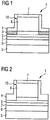
- a radiation-emitting semiconductor chip 1 is shown, which is a laser diode chip.
- the laser diode chip is a strip laser and has a web 10.
- the web 10 extends as far as a first waveguide layer 5, which is directly adjacent to the active zone 2, and thus has an etching depth at which a relatively small threshold current can be achieved, but at which higher modes occur without structured areas 3.
- a conventional semiconductor chip without structured areas is in Figure 2 shown.
- the in Figure 1 shown semiconductor chip 1 advantageously at two opposite lying flanks of the web 10 structured areas 3 arranged.
- the structured regions 3 have structural elements (not shown) which are arranged irregularly, have a width b ⁇ and a distance a ⁇ from one another.
- the structural elements can in particular have a width b ⁇ / 4 and a distance a ⁇ / 4 from one another.
- the ratio g: h 1:10, in particular g: h 1:10.
- the structural elements are etched out of the first waveguide layer 5 and thus contain the same material as the first waveguide layer 5.
- the material is a semiconductor material.
- a passivation layer 4 which contains a silicon oxide, for example, forms over the structured areas 3 and fills the spaces between the individual structural elements. Due to the interlocking between the structural elements protruding from the first waveguide layer 5 with the passivation layer 4, the passivation layer 4 adheres particularly well to the waveguide layer 5 . This is because an imaginary intermediate layer which comprises the structural elements and the spaces filled by the passivation layer 4 and thus between the waveguide layer 5 and the passivation layer 4 is arranged, has an effective refractive index n eff , which is between the first refractive index n 1 of the material of the structure elements and the second refractive index n 2 of the passivation layer 4.
- the active zone 2 adjacent to the waveguide layer 5 can have a p-conducting and an n-conducting semiconductor layer, between which a radiation-generating pn junction is arranged.
- the active zone 2 can, however, also have a double heterostructure, a single quantum well structure or a multiple quantum well structure (MQW).
- MQW multiple quantum well structure
- the radiation generated in the active zone 2 is emitted through the edges of the semiconductor chip 1.
- the main emission direction runs parallel to the web 10, which is designed in the form of a strip.
- the active zone 2 is arranged on a second waveguide layer 8.
- the first waveguide layer 5 and the second waveguide layer 8 have different conductivity types.
- the first waveguide layer 5 can be p-conducting and the second waveguide layer 8 can be n-conducting.
- the two waveguide layers 5 and 8 are each delimited by a cladding layer on a side facing away from the active zone 2.
- the first cladding layer 6 has the same conductivity as the first waveguide layer 5 to which it is applied.
- the second cladding layer 9 has the same conductivity type as the second waveguide layer 8, which is applied to the second cladding layer 9.
- All layers except for the passivation layer 4 and a contact layer 7 arranged on the web 10 are preferably grown epitaxially on one another and form a stack of semiconductor layers.
- the semiconductor material of the semiconductor layers can be a material based on a nitride, phosphide or arsenide compound semiconductor.
- a radiation-emitting semiconductor chip 1 which has a structure like that in FIG Figure 1 Has semiconductor chip 1 shown and additionally an absorber layer 11.
- the absorber layer 11 is applied directly to the passivation layer 4.
- the electrical insulation can be influenced independently of the degree of absorption.
- a conventional semiconductor chip 1 as in FIG Figure 4 shown, a single layer is provided for electrical insulation and mode attenuation, namely the absorbing passivation layer 4, which contains a mixture of an electrically insulating material and an absorbing material.
- the refractive index jump in the exemplary embodiment of FIG Figure 3 be reduced. This allows an optical wave to go deeper into the layers penetrate and reach the absorber layer 11.
- the absorber layer 11 preferably contains an oxide or nitride, in particular ITO or an oxide or nitride of Si, Ti, Al, Ga, Nb, Zr, Ta, Hf, Zn, Mg, Rh, In. These materials are particularly suitable for a semiconductor chip based on nitride compound semiconductors, as preferred within the scope of the present invention.
- an oxide or nitride in particular ITO or an oxide or nitride of Si, Ti, Al, Ga, Nb, Zr, Ta, Hf, Zn, Mg, Rh, In.
- a silicon oxide can be used for example.
- FIG. 5 shows a further embodiment of a radiation-emitting semiconductor chip 1 according to the invention.
- the semiconductor chip 1 shown here is a laser array which has a plurality of strip lasers 12 and a plurality of structured areas 3, one structured area 3 in each case being arranged between two adjacent strip lasers 12. By means of the structured areas 3, crosstalk of scattered light from one strip laser to the other can be better suppressed.
- the strip lasers 12 are not individual components. Rather, the semiconductor chip 1 has a continuous active zone 2. Only the front-side contacting of the strip lasers 12 takes place separately by means of the first contact layers 7.
- the strip lasers 12 are like the one in FIG Figure 1 illustrated radiation-emitting semiconductor chip 1 constructed.
- the stripe lasers 12 can, however, also like the one in FIG Figure 3 Shown radiation-emitting semiconductor chip 1 be constructed.
- the refractive index transition between the layer stack and the surroundings and thus the probability of total reflections can be reduced by means of the structured regions 3. This allows stray light to be better coupled out of the semiconductor chip 1, as a result of which crosstalk from one strip laser to the other can be suppressed.
- the scattered light can advantageously be absorbed.
- the structural elements can have a width ⁇ ⁇ b 4 4 ⁇ m. In this case the structural elements act as scattering centers.
- the structural elements can, however, also have a width b ⁇ , in the case of larger wavelengths also b ⁇ / 4, so that the structural elements surrounded by the passivation layer 4 represent an intermediate layer with an effective refractive index n eff .
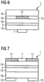
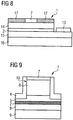
- the Figures 6 to 8 show radiation-emitting semiconductor chips 1.
- the radiation-emitting semiconductor chips 1 are preferably light-emitting diodes which, in contrast to those in the Figures 1 to 5
- the laser diodes shown do not emit any coherent radiation.
- the semiconductor chips 1 of the Figures 6 to 8 What is common is that they have a dielectric mirror 17 with a first dielectric layer (not shown) and a second dielectric layer (not shown).
- the structured area (not shown) is located at the transition between the first and the second dielectric layer.
- FIG. 10 shows a semiconductor chip 1 which is a thin film semiconductor chip.
- the illustrated thin-film semiconductor chip 1 has a layer stack with epitaxially grown semiconductor layers 15, 2, 14 from which the growth substrate has been detached.
- Layer 14 is a first layer with a first conductivity type, which is preferably p-conductive
- layer 15 is a second layer with a second conductivity type, which is preferably n-conductive.
- the layer stack is arranged on the carrier 16, the dielectric mirror 17 being located between the carrier 16 and the layer stack.
- the dielectric mirror 17 does not extend over the entire surface of the stack of layers, but is surrounded by a second contact layer 13, by means of which the active zone 2 is electrically connected to the electrically conductive carrier 16.
- Another electrical contact, the first contact layer 7, is arranged on a side of the active zone 2 facing away from the dielectric mirror 17. This side represents the coupling-out side of the semiconductor chip 1.
- the radiation which is emitted from the active zone 2 in the direction of the dielectric mirror 17 can be reflected in an effective manner in the direction of the coupling-out side, as will be explained below.
- the structural elements with a width b ⁇ are preferably formed from the first layer of the dielectric mirror 17 and surrounded by the second layer of the dielectric mirror 17.
- the first layer contains a first material with a first refractive index n 1 and the second layer contains a second material with a second refractive index n 2 .
- the second layer preferably has inclusions, in particular air inclusions, with a refractive index that is smaller than the second refractive index n 2 . As a result, the second refractive index n 2 and thus the effective refractive index n eff can be reduced.
- the first and second layers may each contain an oxide, nitride or oxynitride of Si, Ti, Al, Ga, Nb, Zr, Ta, Hf, Zn, Mg, Rh, In.
- a corresponding mode of operation is in the Figures 7 and 8th illustrated radiation-emitting semiconductor chips 1 is based. Both semiconductor chips 1 have a transparent substrate 16. The radiation can thus be coupled out through the substrate 16.
- the dielectric mirror 17 is arranged on a side of the semiconductor chip 1 opposite the substrate 16 and thus also on a side of the semiconductor chip 1 which is opposite the coupling-out side.
- the dielectric mirror 17 covers an outer region of the layer stack.
- the first contact layer 7 is arranged in the inner region.
- the semiconductor chip 1 of the Figure 7 the second contact layer 13 is applied to the substrate 16.
- the semiconductor chip 1 has Figure 8 the second contact layer 13 on the second layer 15.
- the first and second layers 14 and 15 as well as the active zone 2 can each consist of a plurality of partial layers. This applies to all of the exemplary embodiments described.
- FIG. 4 shows a radiation-emitting semiconductor chip 1, which is a laser diode and, in terms of structure, largely resembles the strip lasers of FIG Figures 1 to 4 corresponds to.
- the structured region (not designated) with structure elements of width b ⁇ is arranged in the active zone 2.
- the structured area forms a quantum well structure.
- the structured region can be used to achieve improved containment of the charge carriers in the active zone 2.
- a shaping mask 18 is applied to a stack of layers of a semiconductor chip 1 with the layers 7, 6, 5, 2, 8 and 9, which still needs shaping (cf. Figure 10A ).
- the shaping mask 18 can be an etching mask for producing a web 10 (cf. Figure 10B ).
- a mask material 19 is applied to the shaping mask 18, which is used to produce the structured area 3 (cf. Figure 10C ) is provided.
- the mask material 19 is arranged at a distance from the regions 30 to be structured.
- the mask material 19 can be a metal, for example Ni, Ti or Pt, a dielectric material, for example an oxide or nitride of Si, Ti or Zr, or contain a polymer, for example a photoresist.
- a protective layer 20 can be applied to the mask material 19.
- An etching process is carried out to produce the web 10 (cf. Figure 10B ).
- the first contact layer 7 and the first waveguide layer 6 are structured in such a way that the web 10 is formed.
- the protective layer 20 is completely etched away.
- the etching depth of the web 10 can be increased by further etching.
- the mask material 19, which is used to produce the structural elements, is at least partially removed and can be deposited on the areas 30 to be structured (cf. Figure 10B ).
Landscapes
- Physics & Mathematics (AREA)
- Geometry (AREA)
- Condensed Matter Physics & Semiconductors (AREA)
- General Physics & Mathematics (AREA)
- Electromagnetism (AREA)
- Optics & Photonics (AREA)
- Semiconductor Lasers (AREA)
- Led Devices (AREA)
Claims (11)
- Puce semi-conductrice (1) émettant un rayonnement comportant- une zone active (2) pour générer un rayonnement de longueur d'onde λ,- une région structurée (3) comportant des éléments structuraux disposés de manière irrégulière, comprenant un premier matériau ayant un premier indice de réfraction n1 et sont entourée d'un milieu qui comporte un deuxième matériau ayant un deuxième indice de réfraction n2, dans laquelle- l'épaisseur d'une couche intermédiaire comprenant les éléments structuraux et le milieu correspond à une hauteur maximale des éléments structuraux, dans laquelle, pour un indice de réfraction effectif neff de la couche intermédiaire n2 < neff < n1 s'applique- la puce semi-conductrice (1) est un laser à bande ayant une barre (10), dans laquelle la région structurée (3) pour le découplage de la lumière diffusée étant disposée à côté de l'barre (10), caractérisé en ce que- une largeur de base g des éléments structuraux respectifs est inférieure à une hauteur h des éléments structuraux respectifs, et- le milieu est une couche de passivation (4) ou une couche absorbante (11) recouvrant les éléments structuraux.
- Puce semi-conductrice (1) émettant un rayonnement selon la revendication 1, dans laquelle
les éléments structuraux présentent respectivement une largeur b ≤ 4µm et une distance a ≤ 4µm les uns par rapport aux autres. - Puce semi-conductrice (1) émettant un rayonnement selon la revendication 1, dans laquelle
les éléments structuraux ont respectivement une largeur b ≤ λ et une distance a ≤ λ les uns par rapport aux autres. - Puce semi-conductrice (1) émettant un rayonnement selon la revendication 1, dans laquelle
l'indice de réfraction effectif neff est fixé par la concentration du premier matériau par rapport à la concentration du deuxième matériau dans la couche intermédiaire. - Puce semi-conductrice (1) émettant un rayonnement selon l'une quelconque des revendications précédentes, dans laquelle la région structurée (3) est disposée sur les flancs de la barre (10).
- Puce semi-conductrice (1) émettant un rayonnement selon la revendication 5, dans laquelle les éléments structuraux sont formés d'une couche semi-conductrice de la puce semi-conductrice (1).
- Puce semi-conductrice (1) émettant un rayonnement selon l'une quelconque des revendications 1 ou 3 à 4, comprenant un miroir diélectrique (17), dans laquelle les éléments structuraux sont formés d'une première couche du miroir diélectrique (17) et entourés d'une deuxième couche du miroir diélectrique (17).
- Puce semi-conductrice (1) émettant un rayonnement selon l'une quelconque des revendications 1 à 3, dans laquelle la zone active (2) comprend la région structurée (2) formant une structure de puits quantique.
- Puce semi-conductrice (1) émettant un rayonnement selon la revendication 1,
qui est une diode électroluminescente, dans lequel la région structurée (3) est une couche de découplage de la diode électroluminescente. - Procédé de fabrication d'une puce semi-conductrice (1) selon l'une quelconque des revendications précédentes, dans lequel une couche de masque avec des interruptions est appliquée sur la région (30) devant être structurée et la région (30) est gravée dans les interruptions, de sorte qu'après décollement de la couche de masque, la région structurée (3) est formée avec les éléments structuraux.
- Procédé de fabrication d'une puce semi-conductrice (1) selon l'une quelconque des revendications 1 à 9, dans lequel un matériau de masque (19) est disposé à distance d'une région (30) devant être structurée, est au moins partiellement éliminé lors d'un processus de gravure et est déposé sur la région (30) devant être structurée, la région (30) devant être structurée étant simultanément gravée de sorte que les éléments structuraux sont formés.
Applications Claiming Priority (4)
| Application Number | Priority Date | Filing Date | Title |
|---|---|---|---|
| DE102007046497 | 2007-09-28 | ||
| DE102007060204.0A DE102007060204B4 (de) | 2007-09-28 | 2007-12-14 | Strahlung emittierender Halbleiterchip |
| EP08834637.4A EP2193556B1 (fr) | 2007-09-28 | 2008-08-27 | Puce semi-conductrice émettant un rayonnement |
| PCT/DE2008/001423 WO2009039811A2 (fr) | 2007-09-28 | 2008-08-27 | Puce semi-conductrice émettant un rayonnement |
Related Parent Applications (2)
| Application Number | Title | Priority Date | Filing Date |
|---|---|---|---|
| EP08834637.4A Division EP2193556B1 (fr) | 2007-09-28 | 2008-08-27 | Puce semi-conductrice émettant un rayonnement |
| EP08834637.4A Division-Into EP2193556B1 (fr) | 2007-09-28 | 2008-08-27 | Puce semi-conductrice émettant un rayonnement |
Publications (2)
| Publication Number | Publication Date |
|---|---|
| EP3206239A1 EP3206239A1 (fr) | 2017-08-16 |
| EP3206239B1 true EP3206239B1 (fr) | 2021-06-30 |
Family
ID=40435571
Family Applications (2)
| Application Number | Title | Priority Date | Filing Date |
|---|---|---|---|
| EP17157898.2A Active EP3206239B1 (fr) | 2007-09-28 | 2008-08-27 | Puce semi-conductrice émettant un rayonnement |
| EP08834637.4A Active EP2193556B1 (fr) | 2007-09-28 | 2008-08-27 | Puce semi-conductrice émettant un rayonnement |
Family Applications After (1)
| Application Number | Title | Priority Date | Filing Date |
|---|---|---|---|
| EP08834637.4A Active EP2193556B1 (fr) | 2007-09-28 | 2008-08-27 | Puce semi-conductrice émettant un rayonnement |
Country Status (9)
| Country | Link |
|---|---|
| US (1) | US8340146B2 (fr) |
| EP (2) | EP3206239B1 (fr) |
| JP (2) | JP2010541215A (fr) |
| KR (2) | KR101718271B1 (fr) |
| CN (1) | CN101809772B (fr) |
| DE (2) | DE102007060204B4 (fr) |
| PL (1) | PL2193556T3 (fr) |
| TW (1) | TWI385827B (fr) |
| WO (1) | WO2009039811A2 (fr) |
Families Citing this family (8)
| Publication number | Priority date | Publication date | Assignee | Title |
|---|---|---|---|---|
| DE102011100175B4 (de) | 2011-05-02 | 2021-12-23 | OSRAM Opto Semiconductors Gesellschaft mit beschränkter Haftung | Laserlichtquelle mit einer Stegwellenleiterstruktur und einer Modenfilterstruktur |
| DE102012103549B4 (de) | 2012-04-23 | 2020-06-18 | Osram Opto Semiconductors Gmbh | Halbleiterlaserlichtquelle mit einem kantenemittierenden Halbleiterkörper und Licht streuenden Teilbereich |
| DE102013216527A1 (de) | 2013-08-21 | 2015-02-26 | Osram Opto Semiconductors Gmbh | Laserbauelement und Verfahren zum Herstellen eines Laserbauelements |
| KR20160034534A (ko) | 2014-09-19 | 2016-03-30 | 삼성전자주식회사 | 반도체 발광 소자 |
| KR101689468B1 (ko) * | 2015-05-19 | 2016-12-26 | 주식회사 솔탑 | 라이다식 운고계 장치 및 라이다식 운고계 장치 구현 방법 |
| DE102016106495A1 (de) * | 2016-04-08 | 2017-10-12 | Osram Opto Semiconductors Gmbh | Halbleiterlaser |
| JP7222217B2 (ja) | 2018-10-30 | 2023-02-15 | Tdk株式会社 | 積層コイル部品 |
| CN115775859B (zh) * | 2022-11-09 | 2026-02-17 | 京东方华灿光电(浙江)有限公司 | 改善光串扰的发光二极管及其制备方法 |
Citations (1)
| Publication number | Priority date | Publication date | Assignee | Title |
|---|---|---|---|---|
| EP1012933B1 (fr) * | 1997-01-27 | 2004-09-22 | International Business Machines Corporation | Dispositif laser |
Family Cites Families (16)
| Publication number | Priority date | Publication date | Assignee | Title |
|---|---|---|---|---|
| JPS61108176A (ja) | 1984-11-01 | 1986-05-26 | Fuji Electric Co Ltd | 粗面化方法 |
| JP2755357B2 (ja) * | 1991-08-30 | 1998-05-20 | シャープ株式会社 | 半導体レーザ素子 |
| JP3448441B2 (ja) * | 1996-11-29 | 2003-09-22 | 三洋電機株式会社 | 発光装置 |
| JP5019664B2 (ja) * | 1998-07-28 | 2012-09-05 | アイメック | 高効率で光を発するデバイスおよびそのようなデバイスの製造方法 |
| JP3633447B2 (ja) * | 1999-09-29 | 2005-03-30 | 豊田合成株式会社 | Iii族窒化物系化合物半導体素子 |
| US6515305B2 (en) * | 2000-09-18 | 2003-02-04 | Regents Of The University Of Minnesota | Vertical cavity surface emitting laser with single mode confinement |
| JP4117778B2 (ja) * | 2002-09-27 | 2008-07-16 | 日本電信電話株式会社 | 半導体光素子 |
| DE602004011146T2 (de) * | 2003-06-27 | 2008-12-24 | Nichia Corp., Anan | Nitrid-Halbleiterlaser mit Stromsperrschichten und Herstellungsverfahren hierfür |
| TWI330413B (en) * | 2005-01-25 | 2010-09-11 | Epistar Corp | A light-emitting device |
| JP4830315B2 (ja) | 2004-03-05 | 2011-12-07 | 日亜化学工業株式会社 | 半導体レーザ素子 |
| KR100674836B1 (ko) | 2005-02-28 | 2007-01-26 | 삼성전기주식회사 | 고출력 단일모드 반도체 레이저소자 및 그 제조방법 |
| US20060204865A1 (en) * | 2005-03-08 | 2006-09-14 | Luminus Devices, Inc. | Patterned light-emitting devices |
| JP4852972B2 (ja) * | 2005-10-26 | 2012-01-11 | パナソニック電工株式会社 | 光学部品の製造方法及び発光素子 |
| JP2007134445A (ja) * | 2005-11-09 | 2007-05-31 | Nichia Chem Ind Ltd | 窒化物半導体レーザ素子 |
| JP4959203B2 (ja) * | 2006-02-17 | 2012-06-20 | 昭和電工株式会社 | 発光素子及びその製造方法、並びにランプ |
| DE102006017573A1 (de) * | 2006-04-13 | 2007-10-18 | Osram Opto Semiconductors Gmbh | Optoelektronischer Halbleiterkörper und Verfahren zu dessen Herstellung |
-
2007
- 2007-12-14 DE DE102007060204.0A patent/DE102007060204B4/de active Active
- 2007-12-14 DE DE102007063957.2A patent/DE102007063957B3/de active Active
-
2008
- 2008-08-27 US US12/679,832 patent/US8340146B2/en active Active
- 2008-08-27 EP EP17157898.2A patent/EP3206239B1/fr active Active
- 2008-08-27 WO PCT/DE2008/001423 patent/WO2009039811A2/fr not_active Ceased
- 2008-08-27 JP JP2010526146A patent/JP2010541215A/ja active Pending
- 2008-08-27 CN CN2008801093260A patent/CN101809772B/zh active Active
- 2008-08-27 KR KR1020157022923A patent/KR101718271B1/ko active Active
- 2008-08-27 PL PL08834637T patent/PL2193556T3/pl unknown
- 2008-08-27 EP EP08834637.4A patent/EP2193556B1/fr active Active
- 2008-08-27 KR KR1020107009391A patent/KR101567613B1/ko active Active
- 2008-09-02 TW TW097133529A patent/TWI385827B/zh not_active IP Right Cessation
-
2013
- 2013-12-26 JP JP2013269316A patent/JP2014057113A/ja active Pending
Patent Citations (1)
| Publication number | Priority date | Publication date | Assignee | Title |
|---|---|---|---|---|
| EP1012933B1 (fr) * | 1997-01-27 | 2004-09-22 | International Business Machines Corporation | Dispositif laser |
Also Published As
| Publication number | Publication date |
|---|---|
| DE102007060204B4 (de) | 2019-02-28 |
| KR101567613B1 (ko) | 2015-11-09 |
| PL2193556T3 (pl) | 2017-12-29 |
| KR20150104637A (ko) | 2015-09-15 |
| US20100278203A1 (en) | 2010-11-04 |
| DE102007063957B3 (de) | 2022-10-27 |
| WO2009039811A2 (fr) | 2009-04-02 |
| KR20100089833A (ko) | 2010-08-12 |
| TWI385827B (zh) | 2013-02-11 |
| DE102007060204A1 (de) | 2009-04-16 |
| JP2010541215A (ja) | 2010-12-24 |
| WO2009039811A3 (fr) | 2009-09-03 |
| TW200917534A (en) | 2009-04-16 |
| CN101809772A (zh) | 2010-08-18 |
| JP2014057113A (ja) | 2014-03-27 |
| CN101809772B (zh) | 2012-09-05 |
| EP3206239A1 (fr) | 2017-08-16 |
| EP2193556B1 (fr) | 2017-07-26 |
| EP2193556A2 (fr) | 2010-06-09 |
| US8340146B2 (en) | 2012-12-25 |
| KR101718271B1 (ko) | 2017-03-20 |
Similar Documents
| Publication | Publication Date | Title |
|---|---|---|
| EP2260516B1 (fr) | Puce semiconductrice optoélectronique et procédé de fabrication associé | |
| EP3206239B1 (fr) | Puce semi-conductrice émettant un rayonnement | |
| DE102007022947B4 (de) | Optoelektronischer Halbleiterkörper und Verfahren zur Herstellung eines solchen | |
| EP3200247B1 (fr) | Puce semi-conductrice et procédé de fabrication d'une puce semi-conductrice | |
| EP2015372B1 (fr) | Puce semi-conductrice et procédé de fabrication d'une puce semi-conductrice | |
| WO2012062635A1 (fr) | Puce de semi-conducteur optoélectronique et son procédé de production | |
| DE102011111604B4 (de) | Strahlungsemittierendes Halbleiterbauelement | |
| EP1845564A2 (fr) | Corps émettant des rayonnements et procédé de fabrication d'un corps émettant des rayonnements | |
| EP3206238B1 (fr) | Diode électroluminescente à couches minces dotée d'une couche miroir et son procédé de fabrication | |
| EP1592072B1 (fr) | Dispositif semiconducteur optoélectronique et son procédé de fabrication | |
| DE10229231B4 (de) | Verfahren zum Herstellen eines Strahlung emittierenden und/oder empfangenden Halbleiterchips mit einer Strahlungsein- und/oder -auskoppel-Mikrostruktur | |
| WO2012052415A1 (fr) | Composant optoélectronique et son procédé de fabrication | |
| WO2019020424A1 (fr) | Puce semi-conductrice optoélectronique, puce semi-conductrice à haut voltage et procédé de fabrication d'une puce semi-conductrice optoélectronique | |
| WO2010012256A1 (fr) | Puce semiconductrice optoélectronique | |
| DE102013200509A1 (de) | Optoelektronischer Halbleiterchip | |
| WO2004032248A2 (fr) | Composant semi-conducteur emetteur de rayonnement et son procede de production | |
| WO2016078986A1 (fr) | Procédé de fabrication d'une puce semi-conductrice optoélectronique et puce semi-conductrice optoélectronique | |
| WO2010048918A1 (fr) | Puce de semiconducteur optoélectronique et procédé de fabrication d'une puce de semiconducteur optoélectronique | |
| WO2012139953A1 (fr) | Procédé pour la fabrication d'un corps semi-conducteur | |
| WO2020035498A1 (fr) | Puce semi-conductrice optoélectronique et procédé de fabrication d'une puce semi-conductrice optoélectronique | |
| DE102022119108A1 (de) | Optoelektronisches halbleiterbauelement und verfahren zur herstellung zumindest eines optoelektronischen halbleiterbauelements | |
| DE10162914A1 (de) | Lichtemittierendes Halbleiterbauelement | |
| DE102016102876A1 (de) | Optoelektronisches Halbleiterbauelement und Verfahren zur Herstellung eines optoelektronischen Halbleiterbauelements | |
| DE102018107470A1 (de) | Optoelektronischer halbleiterchip und verfahren zur herstellung eines optoelektronischen halbleiterchips | |
| DE102022117503A1 (de) | Optoelektronisches halbleiterbauelement |
Legal Events
| Date | Code | Title | Description |
|---|---|---|---|
| PUAI | Public reference made under article 153(3) epc to a published international application that has entered the european phase |
Free format text: ORIGINAL CODE: 0009012 |
|
| STAA | Information on the status of an ep patent application or granted ep patent |
Free format text: STATUS: THE APPLICATION HAS BEEN PUBLISHED |
|
| AC | Divisional application: reference to earlier application |
Ref document number: 2193556 Country of ref document: EP Kind code of ref document: P |
|
| AK | Designated contracting states |
Kind code of ref document: A1 Designated state(s): AT BE BG CH CY CZ DE DK EE ES FI FR GB GR HR HU IE IS IT LI LT LU LV MC MT NL NO PL PT RO SE SI SK TR |
|
| STAA | Information on the status of an ep patent application or granted ep patent |
Free format text: STATUS: REQUEST FOR EXAMINATION WAS MADE |
|
| 17P | Request for examination filed |
Effective date: 20171221 |
|
| RBV | Designated contracting states (corrected) |
Designated state(s): AT BE BG CH CY CZ DE DK EE ES FI FR GB GR HR HU IE IS IT LI LT LU LV MC MT NL NO PL PT RO SE SI SK TR |
|
| RAP1 | Party data changed (applicant data changed or rights of an application transferred) |
Owner name: OSRAM OPTO SEMICONDUCTORS GMBH |
|
| REG | Reference to a national code |
Ref country code: DE Ref legal event code: R079 Ref document number: 502008017213 Country of ref document: DE Free format text: PREVIOUS MAIN CLASS: H01L0033440000 Ipc: H01S0005200000 |
|
| GRAP | Despatch of communication of intention to grant a patent |
Free format text: ORIGINAL CODE: EPIDOSNIGR1 |
|
| STAA | Information on the status of an ep patent application or granted ep patent |
Free format text: STATUS: GRANT OF PATENT IS INTENDED |
|
| RIC1 | Information provided on ipc code assigned before grant |
Ipc: H01L 33/44 20100101ALI20200117BHEP Ipc: H01S 5/22 20060101ALI20200117BHEP Ipc: H01S 5/20 20060101AFI20200117BHEP |
|
| INTG | Intention to grant announced |
Effective date: 20200206 |
|
| GRAJ | Information related to disapproval of communication of intention to grant by the applicant or resumption of examination proceedings by the epo deleted |
Free format text: ORIGINAL CODE: EPIDOSDIGR1 |
|
| STAA | Information on the status of an ep patent application or granted ep patent |
Free format text: STATUS: REQUEST FOR EXAMINATION WAS MADE |
|
| INTC | Intention to grant announced (deleted) | ||
| GRAP | Despatch of communication of intention to grant a patent |
Free format text: ORIGINAL CODE: EPIDOSNIGR1 |
|
| STAA | Information on the status of an ep patent application or granted ep patent |
Free format text: STATUS: GRANT OF PATENT IS INTENDED |
|
| INTG | Intention to grant announced |
Effective date: 20210126 |
|
| GRAS | Grant fee paid |
Free format text: ORIGINAL CODE: EPIDOSNIGR3 |
|
| GRAA | (expected) grant |
Free format text: ORIGINAL CODE: 0009210 |
|
| STAA | Information on the status of an ep patent application or granted ep patent |
Free format text: STATUS: THE PATENT HAS BEEN GRANTED |
|
| AC | Divisional application: reference to earlier application |
Ref document number: 2193556 Country of ref document: EP Kind code of ref document: P |
|
| AK | Designated contracting states |
Kind code of ref document: B1 Designated state(s): AT BE BG CH CY CZ DE DK EE ES FI FR GB GR HR HU IE IS IT LI LT LU LV MC MT NL NO PL PT RO SE SI SK TR |
|
| REG | Reference to a national code |
Ref country code: CH Ref legal event code: EP |
|
| REG | Reference to a national code |
Ref country code: DE Ref legal event code: R096 Ref document number: 502008017213 Country of ref document: DE Ref country code: AT Ref legal event code: REF Ref document number: 1407231 Country of ref document: AT Kind code of ref document: T Effective date: 20210715 |
|
| REG | Reference to a national code |
Ref country code: IE Ref legal event code: FG4D Free format text: LANGUAGE OF EP DOCUMENT: GERMAN |
|
| REG | Reference to a national code |
Ref country code: LT Ref legal event code: MG9D |
|
| PG25 | Lapsed in a contracting state [announced via postgrant information from national office to epo] |
Ref country code: FI Free format text: LAPSE BECAUSE OF FAILURE TO SUBMIT A TRANSLATION OF THE DESCRIPTION OR TO PAY THE FEE WITHIN THE PRESCRIBED TIME-LIMIT Effective date: 20210630 Ref country code: HR Free format text: LAPSE BECAUSE OF FAILURE TO SUBMIT A TRANSLATION OF THE DESCRIPTION OR TO PAY THE FEE WITHIN THE PRESCRIBED TIME-LIMIT Effective date: 20210630 Ref country code: BG Free format text: LAPSE BECAUSE OF FAILURE TO SUBMIT A TRANSLATION OF THE DESCRIPTION OR TO PAY THE FEE WITHIN THE PRESCRIBED TIME-LIMIT Effective date: 20210930 |
|
| REG | Reference to a national code |
Ref country code: NL Ref legal event code: MP Effective date: 20210630 |
|
| PG25 | Lapsed in a contracting state [announced via postgrant information from national office to epo] |
Ref country code: GR Free format text: LAPSE BECAUSE OF FAILURE TO SUBMIT A TRANSLATION OF THE DESCRIPTION OR TO PAY THE FEE WITHIN THE PRESCRIBED TIME-LIMIT Effective date: 20211001 Ref country code: LV Free format text: LAPSE BECAUSE OF FAILURE TO SUBMIT A TRANSLATION OF THE DESCRIPTION OR TO PAY THE FEE WITHIN THE PRESCRIBED TIME-LIMIT Effective date: 20210630 Ref country code: NO Free format text: LAPSE BECAUSE OF FAILURE TO SUBMIT A TRANSLATION OF THE DESCRIPTION OR TO PAY THE FEE WITHIN THE PRESCRIBED TIME-LIMIT Effective date: 20210930 Ref country code: SE Free format text: LAPSE BECAUSE OF FAILURE TO SUBMIT A TRANSLATION OF THE DESCRIPTION OR TO PAY THE FEE WITHIN THE PRESCRIBED TIME-LIMIT Effective date: 20210630 |
|
| PG25 | Lapsed in a contracting state [announced via postgrant information from national office to epo] |
Ref country code: SK Free format text: LAPSE BECAUSE OF FAILURE TO SUBMIT A TRANSLATION OF THE DESCRIPTION OR TO PAY THE FEE WITHIN THE PRESCRIBED TIME-LIMIT Effective date: 20210630 Ref country code: EE Free format text: LAPSE BECAUSE OF FAILURE TO SUBMIT A TRANSLATION OF THE DESCRIPTION OR TO PAY THE FEE WITHIN THE PRESCRIBED TIME-LIMIT Effective date: 20210630 Ref country code: CZ Free format text: LAPSE BECAUSE OF FAILURE TO SUBMIT A TRANSLATION OF THE DESCRIPTION OR TO PAY THE FEE WITHIN THE PRESCRIBED TIME-LIMIT Effective date: 20210630 Ref country code: RO Free format text: LAPSE BECAUSE OF FAILURE TO SUBMIT A TRANSLATION OF THE DESCRIPTION OR TO PAY THE FEE WITHIN THE PRESCRIBED TIME-LIMIT Effective date: 20210630 Ref country code: NL Free format text: LAPSE BECAUSE OF FAILURE TO SUBMIT A TRANSLATION OF THE DESCRIPTION OR TO PAY THE FEE WITHIN THE PRESCRIBED TIME-LIMIT Effective date: 20210630 Ref country code: PT Free format text: LAPSE BECAUSE OF FAILURE TO SUBMIT A TRANSLATION OF THE DESCRIPTION OR TO PAY THE FEE WITHIN THE PRESCRIBED TIME-LIMIT Effective date: 20211102 Ref country code: ES Free format text: LAPSE BECAUSE OF FAILURE TO SUBMIT A TRANSLATION OF THE DESCRIPTION OR TO PAY THE FEE WITHIN THE PRESCRIBED TIME-LIMIT Effective date: 20210630 |
|
| PG25 | Lapsed in a contracting state [announced via postgrant information from national office to epo] |
Ref country code: PL Free format text: LAPSE BECAUSE OF FAILURE TO SUBMIT A TRANSLATION OF THE DESCRIPTION OR TO PAY THE FEE WITHIN THE PRESCRIBED TIME-LIMIT Effective date: 20210630 |
|
| REG | Reference to a national code |
Ref country code: DE Ref legal event code: R097 Ref document number: 502008017213 Country of ref document: DE Ref country code: CH Ref legal event code: PL |
|
| PG25 | Lapsed in a contracting state [announced via postgrant information from national office to epo] |
Ref country code: MC Free format text: LAPSE BECAUSE OF FAILURE TO SUBMIT A TRANSLATION OF THE DESCRIPTION OR TO PAY THE FEE WITHIN THE PRESCRIBED TIME-LIMIT Effective date: 20210630 |
|
| REG | Reference to a national code |
Ref country code: BE Ref legal event code: MM Effective date: 20210831 |
|
| PG25 | Lapsed in a contracting state [announced via postgrant information from national office to epo] |
Ref country code: LI Free format text: LAPSE BECAUSE OF NON-PAYMENT OF DUE FEES Effective date: 20210831 Ref country code: DK Free format text: LAPSE BECAUSE OF FAILURE TO SUBMIT A TRANSLATION OF THE DESCRIPTION OR TO PAY THE FEE WITHIN THE PRESCRIBED TIME-LIMIT Effective date: 20210630 Ref country code: CH Free format text: LAPSE BECAUSE OF NON-PAYMENT OF DUE FEES Effective date: 20210831 |
|
| PLBE | No opposition filed within time limit |
Free format text: ORIGINAL CODE: 0009261 |
|
| STAA | Information on the status of an ep patent application or granted ep patent |
Free format text: STATUS: NO OPPOSITION FILED WITHIN TIME LIMIT |
|
| GBPC | Gb: european patent ceased through non-payment of renewal fee |
Effective date: 20210930 |
|
| PG25 | Lapsed in a contracting state [announced via postgrant information from national office to epo] |
Ref country code: LU Free format text: LAPSE BECAUSE OF NON-PAYMENT OF DUE FEES Effective date: 20210827 |
|
| 26N | No opposition filed |
Effective date: 20220331 |
|
| PG25 | Lapsed in a contracting state [announced via postgrant information from national office to epo] |
Ref country code: IT Free format text: LAPSE BECAUSE OF FAILURE TO SUBMIT A TRANSLATION OF THE DESCRIPTION OR TO PAY THE FEE WITHIN THE PRESCRIBED TIME-LIMIT Effective date: 20210630 Ref country code: IE Free format text: LAPSE BECAUSE OF NON-PAYMENT OF DUE FEES Effective date: 20210827 Ref country code: GB Free format text: LAPSE BECAUSE OF NON-PAYMENT OF DUE FEES Effective date: 20210930 Ref country code: FR Free format text: LAPSE BECAUSE OF NON-PAYMENT OF DUE FEES Effective date: 20210830 Ref country code: BE Free format text: LAPSE BECAUSE OF NON-PAYMENT OF DUE FEES Effective date: 20210831 |
|
| REG | Reference to a national code |
Ref country code: AT Ref legal event code: MM01 Ref document number: 1407231 Country of ref document: AT Kind code of ref document: T Effective date: 20210827 |
|
| PG25 | Lapsed in a contracting state [announced via postgrant information from national office to epo] |
Ref country code: AT Free format text: LAPSE BECAUSE OF NON-PAYMENT OF DUE FEES Effective date: 20210827 |
|
| PG25 | Lapsed in a contracting state [announced via postgrant information from national office to epo] |
Ref country code: LT Free format text: LAPSE BECAUSE OF FAILURE TO SUBMIT A TRANSLATION OF THE DESCRIPTION OR TO PAY THE FEE WITHIN THE PRESCRIBED TIME-LIMIT Effective date: 20210630 |
|
| PG25 | Lapsed in a contracting state [announced via postgrant information from national office to epo] |
Ref country code: HU Free format text: LAPSE BECAUSE OF FAILURE TO SUBMIT A TRANSLATION OF THE DESCRIPTION OR TO PAY THE FEE WITHIN THE PRESCRIBED TIME-LIMIT; INVALID AB INITIO Effective date: 20080827 Ref country code: CY Free format text: LAPSE BECAUSE OF FAILURE TO SUBMIT A TRANSLATION OF THE DESCRIPTION OR TO PAY THE FEE WITHIN THE PRESCRIBED TIME-LIMIT Effective date: 20210630 |
|
| P01 | Opt-out of the competence of the unified patent court (upc) registered |
Effective date: 20230825 |
|
| PG25 | Lapsed in a contracting state [announced via postgrant information from national office to epo] |
Ref country code: MT Free format text: LAPSE BECAUSE OF FAILURE TO SUBMIT A TRANSLATION OF THE DESCRIPTION OR TO PAY THE FEE WITHIN THE PRESCRIBED TIME-LIMIT Effective date: 20210630 |
|
| PGFP | Annual fee paid to national office [announced via postgrant information from national office to epo] |
Ref country code: DE Payment date: 20250820 Year of fee payment: 18 |
|
| PG25 | Lapsed in a contracting state [announced via postgrant information from national office to epo] |
Ref country code: TR Free format text: LAPSE BECAUSE OF FAILURE TO SUBMIT A TRANSLATION OF THE DESCRIPTION OR TO PAY THE FEE WITHIN THE PRESCRIBED TIME-LIMIT Effective date: 20210630 |