EP3206300B1 - Amplificateur de déphasage - Google Patents
Amplificateur de déphasage Download PDFInfo
- Publication number
- EP3206300B1 EP3206300B1 EP16154891.2A EP16154891A EP3206300B1 EP 3206300 B1 EP3206300 B1 EP 3206300B1 EP 16154891 A EP16154891 A EP 16154891A EP 3206300 B1 EP3206300 B1 EP 3206300B1
- Authority
- EP
- European Patent Office
- Prior art keywords
- signal
- phase
- branch
- branch signal
- filtered
- Prior art date
- Legal status (The legal status is an assumption and is not a legal conclusion. Google has not performed a legal analysis and makes no representation as to the accuracy of the status listed.)
- Active
Links
Images




Classifications
-
- H—ELECTRICITY
- H03—ELECTRONIC CIRCUITRY
- H03F—AMPLIFIERS
- H03F1/00—Details of amplifiers with only discharge tubes, only semiconductor devices or only unspecified devices as amplifying elements
- H03F1/42—Modifications of amplifiers to extend the bandwidth
-
- H—ELECTRICITY
- H04—ELECTRIC COMMUNICATION TECHNIQUE
- H04B—TRANSMISSION
- H04B7/00—Radio transmission systems, i.e. using radiation field
- H04B7/24—Radio transmission systems, i.e. using radiation field for communication between two or more posts
- H04B7/26—Radio transmission systems, i.e. using radiation field for communication between two or more posts at least one of which is mobile
-
- H—ELECTRICITY
- H03—ELECTRONIC CIRCUITRY
- H03F—AMPLIFIERS
- H03F1/00—Details of amplifiers with only discharge tubes, only semiconductor devices or only unspecified devices as amplifying elements
- H03F1/02—Modifications of amplifiers to raise the efficiency, e.g. gliding Class A stages, use of an auxiliary oscillation
- H03F1/0205—Modifications of amplifiers to raise the efficiency, e.g. gliding Class A stages, use of an auxiliary oscillation in transistor amplifiers
- H03F1/0294—Modifications of amplifiers to raise the efficiency, e.g. gliding Class A stages, use of an auxiliary oscillation in transistor amplifiers using vector summing of two or more constant amplitude phase-modulated signals
-
- H—ELECTRICITY
- H03—ELECTRONIC CIRCUITRY
- H03F—AMPLIFIERS
- H03F3/00—Amplifiers with only discharge tubes or only semiconductor devices as amplifying elements
- H03F3/189—High-frequency amplifiers, e.g. radio frequency amplifiers
- H03F3/19—High-frequency amplifiers, e.g. radio frequency amplifiers with semiconductor devices only
-
- H—ELECTRICITY
- H04—ELECTRIC COMMUNICATION TECHNIQUE
- H04W—WIRELESS COMMUNICATION NETWORKS
- H04W52/00—Power management, e.g. Transmission Power Control [TPC] or power classes
- H04W52/04—Transmission power control [TPC]
- H04W52/52—Transmission power control [TPC] using AGC [Automatic Gain Control] circuits or amplifiers
-
- H—ELECTRICITY
- H03—ELECTRONIC CIRCUITRY
- H03F—AMPLIFIERS
- H03F2200/00—Indexing scheme relating to amplifiers
- H03F2200/336—A I/Q, i.e. phase quadrature, modulator or demodulator being used in an amplifying circuit
-
- H—ELECTRICITY
- H03—ELECTRONIC CIRCUITRY
- H03F—AMPLIFIERS
- H03F2200/00—Indexing scheme relating to amplifiers
- H03F2200/451—Indexing scheme relating to amplifiers the amplifier being a radio frequency amplifier
-
- H—ELECTRICITY
- H04—ELECTRIC COMMUNICATION TECHNIQUE
- H04L—TRANSMISSION OF DIGITAL INFORMATION, e.g. TELEGRAPHIC COMMUNICATION
- H04L27/00—Modulated-carrier systems
- H04L27/18—Phase-modulated carrier systems, i.e. using phase-shift keying
- H04L27/20—Modulator circuits; Transmitter circuits
- H04L27/2032—Modulator circuits; Transmitter circuits for discrete phase modulation, e.g. in which the phase of the carrier is modulated in a nominally instantaneous manner
- H04L27/2053—Modulator circuits; Transmitter circuits for discrete phase modulation, e.g. in which the phase of the carrier is modulated in a nominally instantaneous manner using more than one carrier, e.g. carriers with different phases
- H04L27/206—Modulator circuits; Transmitter circuits for discrete phase modulation, e.g. in which the phase of the carrier is modulated in a nominally instantaneous manner using more than one carrier, e.g. carriers with different phases using a pair of orthogonal carriers, e.g. quadrature carriers
-
- H—ELECTRICITY
- H04—ELECTRIC COMMUNICATION TECHNIQUE
- H04L—TRANSMISSION OF DIGITAL INFORMATION, e.g. TELEGRAPHIC COMMUNICATION
- H04L27/00—Modulated-carrier systems
- H04L27/32—Carrier systems characterised by combinations of two or more of the types covered by groups H04L27/02, H04L27/10, H04L27/18 or H04L27/26
- H04L27/34—Amplitude- and phase-modulated carrier systems, e.g. quadrature-amplitude modulated carrier systems
- H04L27/36—Modulator circuits; Transmitter circuits
- H04L27/361—Modulation using a single or unspecified number of carriers, e.g. with separate stages of phase and amplitude modulation
-
- H—ELECTRICITY
- H04—ELECTRIC COMMUNICATION TECHNIQUE
- H04L—TRANSMISSION OF DIGITAL INFORMATION, e.g. TELEGRAPHIC COMMUNICATION
- H04L27/00—Modulated-carrier systems
- H04L27/32—Carrier systems characterised by combinations of two or more of the types covered by groups H04L27/02, H04L27/10, H04L27/18 or H04L27/26
- H04L27/34—Amplitude- and phase-modulated carrier systems, e.g. quadrature-amplitude modulated carrier systems
- H04L27/36—Modulator circuits; Transmitter circuits
- H04L27/362—Modulation using more than one carrier, e.g. with quadrature carriers, separately amplitude modulated
Definitions
- the present disclosure relates to an outphasing amplifier, and to a method for mitigating bandwidth expansion in an outphasing amplifier.
- Amplitude modulation is used (with or without the addition of phase modulation) in a wide variety of communications systems such as mobile phones, cellular base stations for mobile phones and satellite communications.
- outphasing amplifiers such as Chireix amplifiers.
- an outphasing amplifier the amplitude part of an amplitude (and phase) modulated input signal is converted into two phase modulated signals, with constant amplitude envelopes.
- the phase modulated signals include the phase of the original signal as a common part, and additional antiphase components that, when recombination occurs, recreate the amplitude content of the original signal.
- the phase modulated signals are amplified by a pair of branch amplifiers, and combined to provide an amplified amplitude modulated output signal. Because of the constant amplitude envelope of the phase modulated signals passed to the branch amplifiers, the branch amplifiers can be operated at saturation, resulting in maximum efficiency.
- US 2013049861 A1 discloses a linear amplification with nonlinear components (LINC) modulator.
- US 2008075194 A1 discloses architectures including digital outphasing transmitters.
- an outphasing amplifier having: a first branch arranged to receive and process a first branch signal, the first branch signal being phase modulated, with constant amplitude envelope; and a second branch arranged to receive and process a second branch signal, the second branch signal being phase modulated, with constant amplitude envelope, and at least a portion of the second branch signal anti-phase from the first branch signal, wherein each branch includes: circuitry arranged to process the signal to reduce the energy in sidebands of the signal away from the central frequency, while retaining the phase information in the signal; and an amplifier arranged to amplify the filtered and re-asserted branch signal.
- the circuitry arranged to process the signal includes: a frequency filter arranged to filter the branch signal to reduce the bandwidth of the branch signal; and a reconstructor arranged to modify at least a portion of the filtered branch signal, to reassert the phase information from the unfiltered branch signal.
- the reconstructor may be arranged to modify the phase of at least a portion of the filtered branch signal based on information taken from the unfiltered branch signal.
- the branch signal comprises information encoded in in-phase and quadrature components, and wherein the filter is arranged to filter the in-phase and quadrature components separately.
- the reconstructor includes: a first converter arranged to convert the filtered in-phase and quadrature components into first magnitude and phase information; a second converter arranged to convert the unfiltered in-phase and quadrature components into second magnitude and phase information; and a third converter arranged to convert the magnitude of the first magnitude and phase information and the angle of the second magnitude and phase information into output in-phase and quadrature information, the filtered and re-asserted branch signal comprising the output in-phase and quadrature components.
- the circuitry may be arranged to filter and reassert the branch signal a plurality of times.
- the branch signal may comprise a first range of frequencies, extending around a central frequency; and the processed signal comprises the first range of frequencies, wherein the energy in the filtered and re-asserted branch signal away from the central frequency is reduced compared to the unfiltered branch signal.
- the outphasing amplifier may include: a signal separator arranged to receive an amplitude modulated RF input signal, and arranged to generate the first branch signal and the second branch signal from the input signal, such that combination of the processed first branch signal and the processed second branch signal provides an amplified version of the input signal.
- the input signal may comprise information encoded in in-phase and quadrature components, the outphasing amplifier comprising: a first digital to analogue converter for generating the in-phase component of the input signal; and a second digital to analogue converter for generating the quadrature component, wherein the reduction of energy in the sidebands reduces the required operational bandwidth of the first digital to analogue converter and the second digital to analogue converter.
- the outphasing amplifier comprising: a first digital to analogue converter for generating the in-phase component of the input signal; and a second digital to analogue converter for generating the quadrature component, wherein the reduction of energy in the sidebands reduces the required operational bandwidth of the first digital to analogue converter and the second digital to analogue converter.
- the outphasing amplifier including a first branch arranged to receive and process a first branch signal, the first branch signal being phase modulated, with constant amplitude envelope, and a second branch arranged to receive and process a second branch signal, the second branch signal being phase modulated, with constant amplitude envelope, and at least a portion of the second branch signal anti-phase from the first branch signal, the method including, in each branch: processing the branch signal to reduce energy in sidebands of the signal away from the central frequency, while retaining the phase information in the signal; and amplifying the processed signal.
- Processing the branch signal includes: filtering the branch signal to reduce the bandwidth of the branch signal; and modifying at least a portion of the filtered branch signal, to reassert the phase information from the unfiltered branch signal.
- Modifying at least a portion of the filtered branch signal may include: modifying the phase of at least a portion of the filtered branch signal based on information taken from the unfiltered branch signal.
- the branch signal comprises information encoded in in-phase and quadrature components, and wherein the filter filters the in-phase and quadrature components separately.
- the method includes: converting the filtered in-phase and quadrature components into first magnitude and phase information; converting the unfiltered in-phase and quadrature components into second magnitude and phase information; and converting the magnitude of the first magnitude and phase information and the angle of the second magnitude and phase information into output in-phase and quadrature information, the filtered and re-asserted branch signal comprising the output in-phase and quadrature components.
- a base station for mobile phone or cellular communications comprising the outphasing amplifier according to the first aspect.
- FIG. 1 shows a schematic illustration of an outphasing amplifier 100.
- An amplitude modulated RF input signal S in is provided to the RF input node 102 of the outphasing amplifier 100.
- the input signal is then passed to a signal separator 104, which separates the amplitude modulated input signal S in into two separate phase modulated signals S 1 , S 2 (branch signals).
- the branch signals S 1 , S 2 both have a constant amplitude envelope, and are identical, but are separated in phase by an outphasing angle.
- ⁇ ( t ) is the outphasing angle of the amplifier.
- the first branch signal S 1 is passed onto a first amplification branch 106 of the outphasing amplifier 100.
- the first amplification branch 106 includes a first branch amplifier 108 which amplifies the first branch signal S 1 to give a first amplified signal component S 1 '.
- the second branch signal S 2 is passed onto a second amplification branch 110 of the outphasing amplifier 100.
- the second amplification branch 110 includes a second branch amplifier 112 which amplifies the second branch signal S 2 to give a second amplified signal component S 2 '.
- g 1 and g 2 are the gains of the first 108 and second 112 branch amplifiers respectively.
- the branch amplifiers 108, 112 have the same gain. In other examples, the branch amplifiers 108, 112 may have different gains.
- the amplified signal components S 1 ', S 2 ' are passed to a combiner 114, where they are summed to give the amplified output signal S out .
- the amplified output signal S out is simply a scaled increase of the input signal S in . Therefore, the outphasing amplifier 100 has amplified the input signal S in by a factor G. G is the gain of the outphasing amplifier 100.
- the output signal S out may be provided for transmission or further downstream processing.
- this is modelled by the output load 118.
- the output load 118 has a characteristic impedance Z 0 .
- the output signal S out should be impedance matched to the characteristic impedance Z 0 .
- the output signal S out may be passed through an impedance matching network 116 to translate the output signal S out in to an impedance matched signal S imp .
- Impedance matching networks are well known in the art of amplifiers.
- the input signal S in and output signal S out include information (amplitude and phase) encoded in baseband as in-phase (I) and quadrature (Q) components.
- Figure 2 schematically illustrates a baseband unit 200 that can be used to generate the input signal S in .
- single ended representation can be used in baseband, requiring fewer but higher performance data converters.
- the I and Q components of the signal are generated as separate digital components by the base station.
- the digital I component is converted into a first analogue signal by a first digital to analogue converter 202a
- the digital Q component is converted into a second analogue signal by a second digital to analogue converter 202b.
- the first analogue signal is filtered by a first filter 204a, and the second analogue signal is filtered by a second filter 204b.
- the filters 204 are digital to analogue converter reconstruction filters, as required by digital to analogue converters.
- the filtered analogue signals are then provided to a quadrature modulator 206, where they are mixed with a signal from a local oscillator 208, and summed to provide the input signal S in .
- the quadrature modulator 206 includes a first modulator 206a for mixing the first analogue signal with the output of the local oscillator, and a second modulator 206b for mixing the second analogue signal with the output of the local oscillator 208. Before mixing with the second analogue signal, the output of the oscillator 208 is passed through a 90 degree phase shift 206c.
- the quadrature modulator 206 also includes a summer 206d for summing the mixed analogue signals.
- Figure 3A illustrates the frequency spectrum of a 20MHz RF input signal, S in .
- the x-axis shows the frequency variation from 20MHz.
- the input signal S in is of relatively narrow bandwidth, with the amplitude of the signal (and hence information in the signal) dropping off away from the main frequency.
- Figure 3B illustrates the frequency spectrum of the outphased signal (S 1 or S 2 ) generated from the input signal of Figure 3A .
- the signal is now of wide bandwidth. This is known as bandwidth expansion. Wideband signals place greater power requirements on the digital to analogue converters 202, modulators 206a,b, and filter circuitry 204 in the baseband unit 200, and in the branches of the amplifier 106, 110, and the branch amplifiers 108, 112.
- FIG. 4 illustrates the steps of a method 300 for mitigating the effect of bandwidth expansion, according to an embodiment.
- each of the branch signals is processed to reduce the energy in the wide bandwidths, created by the translation to phase only information content.
- the wide bandwidths are the frequencies away from the central frequency of the signal.
- the reduction of the power in the wide bandwidths reduces the bandwidth requirements for the components of the amplifier 100, reducing component cost and power consumption.
- the processing of the signal preserves the phase information, so no data is lost from the signal.
- the processing includes a step of filtering 306 the branch signal to reduce the bandwidth of the signal, and a step of modifying the filtered branch signal 308 to reassert the phase information.
- the reasserting of the phase information ensures no phase information is lost, and can be seen as reintroducing phase accuracy into the branch signal after the filtering, or as altering the amplitude of the branch signal after filtering to restore the content of the original signal.
- the input signal S in is received 302.
- the input signal is split 304, into the outphased branch signals of constant amplitude envelope S 1 , S 2 .
- the first branch signal S 1 is filtered 306a on the first branch 106 of the amplifier 100, and the second branch signal S 2 is filtered on the second branch 110 of the amplifier 100.
- the filtering reduces the bandwidth of the outphased signals S 1 , S 2 .
- the filtering is by a simple band-pass filter that only allows frequency components within a predefined range around the central frequency to pass.
- the band pass bandwidth may be 1/3 the sample rate of the system.
- a lower bandwidth signal equates to lower specification hardware in the RF signal generation system, reducing component cost and complexity.
- the band pass bandwidth of 1/3 the sample rate is by way of example only, and any suitable bandwidth may be used.
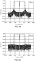
- Figure 5A shows a spectrum of an output signal S out generated by combining two amplified outphased signals, S 1 ', S 2 ', which have been filtered prior to amplification.
- the dashed line shows the shape of the filter applied to the outphased signals.
- the filtering step 306 results in sidebands with high amplitude (and thus high energy). These sidebands result in distortion on the signal, and also mean that the signal is still wideband. Furthermore, because the branch signals are phase modulated, carrying information in their phase, filtering can result in loss of information in the signal.
- the first branch signal S 1 is modified 308a to reintroduce phase information from the unfiltered signal.
- the effect of this modification is to alter the amplitude of parts of the signal, and reasserts the information from the original signal.
- the second branch signal S 2 is modified 308b in a similar manner.
- Figure 5B shows the spectrum of an output signal S out generated by combining two amplified outphased signals, S 1 ', S 2 ', which have been filtered and reasserted prior to amplification.
- reasserting the information modifies the amplitude in a way that reduces the energy in the sidebands. Since the sidebands are lower energy, the effect of the bandwidth expansion is reduced, as will be discussed below.
- the steps of filtering 306 and reasserting 308 can be repeated.
- FIG. 6A schematically illustrates the processing circuitry 400 required to process the branch signals is to reduce the energy in the wide bandwidths, i.e. those away from the central frequency of the signal.
- the processing circuitry 400 includes a filter 402 to filter the branch signal as discussed above, and a reconstructor 410 to modify the filtered branch signal, as also discussed above.
- Figure 6C shows a portion of the amplifier of Figure 1 , including the processing circuitry 400a, 400b.
- First processing circuitry 400a is provided on the first branch 106, to process the first branch signal S 1 .
- Second, identical, processing circuitry 400b is provided on the second branch to process the second branch signal S 2 .
- FIG. 6B shows one example embodiment of the processing circuitry 400 in more detail.
- the operation of this processing circuitry 400 will now be discussed in relation to a single branch signal S 1 , S 2 , although it will be appreciated that the processing circuitry in both branches 106, 110 will function in the same way.
- the branch signals S 1 , S 2 include information encoded in I and Q components, which are received by the processing circuitry 400.
- the I and Q components may be generated by the signal separator 104, or may be determined from the signals from the signal generator 104 in any suitable manner.
- the filter 402 includes a first filter 402a for filtering the I component, and a second filter 402b for filtering the Q component.
- the filters 402 are as discussed in relation to Figure 4 .
- the reconstructor 410 includes a first converter 404, a second converter 406, and a third converter 408.
- the converters 404, 406, 408 are arranged to alter between different signal representations. Using the I and Q components is only one way of representing information encoded in a signal. An alternative method is to use magnitude (MAG) and angle (ANG) information.
- the converters 404, 406, 408 use a CORDIC algorithm to switch between these two systems.
- the first converter 404 converts the filtered I and Q components into first magnitude and angle information including a first magnitude and a first angle.
- the second converter 406 converts the unfiltered I and Q components into second magnitude and angle information including a second magnitude and a second angle.
- the third converter 408 takes the first magnitude, and the second angle, and converts back to I and Q components.
- the filtered magnitude provides the effect of filtering, whilst the unfiltered angle information reasserts the original phase information.
- the output of the third converter is not the direct I and Q signal, but the information required to generate the I and Q signal.
- This information is passed to respective digital to analogue converters (not shown), and then processed as normal.
- the digital to analogue converters may include reconstruction filters (not shown) as discussed in relation to the digital to analogue converters of Figure 2 . Following the filtering and reassertion, the reconstruction filters introduce minimal distortion.
- the amplifiers 108, 112 are limiting amplifiers, operated at saturation.
- the amplifiers 108, 112 take the output from the processing circuitry, and amplify it.
- the distortion of the limiting amplifier modifies the signal such that the amplified branch signals are of the form required to create the amplified output signal. In this way, the system 100 can be seen to use the distortion of the amplifier 108, 112 to insert additional information lost in filtering.
- the system 100 can be used to amplify digital signals, removing the need for digital to analogue converters, reducing cost and power requirements.
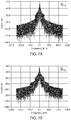
- Figure 7A shows the spectrum of the branch signal following a single iteration of filtering and reassertion.
- Comparison with Figure 3B shows that the outphased, filtered and phase-reasserted signal has lower signal power at wide bandwidths than the original outphased signal. However, the signal at wide bandwidths is higher than in a signal that is only filtered, and so the phase information is not lost, but the bandwidth requirements on the amplifier 100 are reduced.
- the largest reduction of the power occurs at the highest and lowest frequencies, and the central frequency is largely unaffected.
- the power reduction gradually increases from the central frequency to the widest frequencies. In general, the power reduction is most significant in the frequencies outside of the pass band of the filter, although some reduction in power may be seen at frequencies within the pass band.
- Figure 7B shows the spectrum of the branch signal after two iterations of filtering and reassertion. As can be seen the signal power (amplitude) at wide bandwidths is further reduced.
- the filtering and reassertion is repeated for a fixed number of iterations, for example four iterations. The fixed number depends on the type of signal, and the requirements of the output signal. In other examples, the filtering and reassertion is repeated until a threshold criteria is met.
- the threshold criteria may be a predetermined number of iterations, a predetermined processing time, or a predetermined change in the signal. In some situations, multiple threshold criteria may be used, and the filtering and reassertion stopped when the first criteria is met.
- the bandwidth (and hence power) requirements of the amplifier 100 architecture is reduced. Being able to use an operating bandwidth lower than would be required to generate a full bandwidth outphasing signal means lower component and system cost, lower power consumption, and offers increased scope for integration.
- the processing circuitry 400 can be implemented in a field programmable gate array (FPGA) or a complementary metal-oxide semiconductor (CMOS) integrated circuit. It is also compatible with CMOS drivers for the branch amplifiers.
- FPGA field programmable gate array
- CMOS complementary metal-oxide semiconductor
- an amplifier 100 including the processing circuitry can be implemented in a single chip, although this is not necessary.
- the iterations of filtering and reasserting may be provided by routing the signal through the same processing circuitry 400 a number of times.
- separate processing circuitry 400 can be provided for each iteration.
- the pass band of the filter may change for each iteration.
- the pass band may be the same for each iteration.
- the method 300 of mitigating bandwidth expansion (and the processing circuitry 400) is compatible with any outphasing amplifier 100 used to amplify an amplitude modulated RF signal.
- the RF signal is only amplitude modulated
- the method 300 of mitigating bandwidth expansion can also be used with signals that have both amplitude and phase modulation.
- the first and second branch signals both have a common part containing the phase information from the original signal, and an antiphase part containing the amplitude information from the original signal.
- the method 300 and circuitry 400 may be used with signals defined by standards such as LTE, WCDMA, GSM-EDGE, Bluetooth, various 802.11 standards, and modulation schemes such as QAM, OFDMA, and many others requiring amplitude as well as phase domain modulation.
- standards such as LTE, WCDMA, GSM-EDGE, Bluetooth, various 802.11 standards, and modulation schemes such as QAM, OFDMA, and many others requiring amplitude as well as phase domain modulation.
- the bandwidths of the signals are theoretically infinite but in practice components are often scaled for between eight and ten times the bandwidth of the input signal. After filtering and reassertion, the components can have a bandwidth limited by the existing system constraints, so that the bandwidth is between three and five times the bandwidth of the input signal.
- the bandwidth requirements without the filtering and reassertion are 100MHz. This can be reduced to 50MHz by including two iterations of filtering and reassertion. This may be, for example, a signal with bandwidth of 10MHz. In other examples, the bandwidth may be lower or higher.
- a WCDMA signal of 5MHz bandwidth may require between 40 MHz and 50MHz bandwidth without filtering and reassertion, and between 15MHz and 20MHz when using the new technique. It will be evident to those skilled in the art that this concept is as applicable to systems optimised for 100MHz bandwidth LTE signals as it is to a single 3G 5MHZ carrier configuration.
- any suitable method may be implemented in any suitable apparatus.
- any suitable type of filters, converters and digital to analogue converters may be used.
- the converters for example, may be based on algorithms other than a CORDIC algorithm.
- outphasing amplifier 100 and baseband unit 200 discussed above are given by way of example only. Any suitable outphasing amplifier 100 and baseband unit 200 could be used.
- frequencies and signals discussed above are by way of example only, and any suitable frequencies and signals may be used.
Landscapes
- Engineering & Computer Science (AREA)
- Power Engineering (AREA)
- Computer Networks & Wireless Communication (AREA)
- Signal Processing (AREA)
- Amplifiers (AREA)
Claims (9)
- Amplificateur de déphasage (100) ayant :une première branche (106) agencée pour recevoir et traiter un premier signal de branche, le premier signal de branche étant modulé en phase, avec une enveloppe d'amplitude constante ; etune deuxième branche (110) agencée pour recevoir et traiter un deuxième signal de branche, le deuxième signal de branche étant modulé en phase, avec une enveloppe d'amplitude constante, et au moins une partie du deuxième signal de branche étant en opposition de phase avec le premier signal de branche,chaque branche (106, 110) comprenant :des circuits (400) agencés pour traiter le signal de branche, le signal de branche comprenant des informations codées dans des composantes en phase et en quadrature, et le circuit (400) comprenant :un filtre de fréquence (402) agencé pour filtrer le signal de branche afin de réduire la largeur de bande du signal de branche, le filtre (402) étant agencé pour filtrer séparément les composantes en phase et en quadrature ;l'amplificateur de déphasage étant caractérisé en ce que le circuit de chaque branche comprend en outre :un reconstructeur (410) agencé pour modifier au moins une partie du signal de branche filtré, pour réaffirmer les informations de phase à partir du signal de branche non filtré, le reconstructeur (410) comprenant :un premier convertisseur (404) agencé pour convertir les composantes en phase et en quadrature filtrées en premières informations d'amplitude et de phase ;un deuxième convertisseur (406) agencé pour convertir les composantes en phase et en quadrature non filtrées en deuxièmes informations d'amplitude et de phase ; etun troisième convertisseur (408) agencé pour :convertir l'amplitude des premières informations d'amplitude et de phase et l'angle des deuxièmes informations d'amplitude et de phase en informations en phase et en quadrature de sortie,fournir un signal de branche filtré et réaffirmé comprenant les composantes en phase et en quadrature de sortie ; etun amplificateur (108, 112) agencé pour amplifier le signal de branche filtré et réaffirmé.
- Amplificateur de déphasage (100) selon la revendication 1, le reconstructeur (410) étant agencé pour modifier la phase d'au moins une partie du signal de branche filtré sur la base d'informations prises à partir du signal de branche non filtré.
- Amplificateur de déphasage (100) selon l'une quelconque des revendications 1 à 2, le circuit (400) étant agencé pour filtrer et réaffirmer le signal de branche une pluralité de fois.
- Amplificateur de déphasage (100) selon n'importe quelle revendication précédente,
le signal de branche comprenant une première plage de fréquences s'étendant autour d'une fréquence centrale ; et
le signal traité comprenant la première plage de fréquences, l'énergie dans le signal de branche filtré et réaffirmé à l'opposé de la fréquence centrale étant réduite par rapport au signal de branche non filtré. - Amplificateur de déphasage (100) selon n'importe quelle revendication précédente, comprenant :
un séparateur de signal (104) agencé pour recevoir un signal d'entrée RF modulé en amplitude, et agencé pour générer le premier signal de branche et le deuxième signal de branche à partir du signal d'entrée, de telle sorte que la combinaison du premier signal de branche traité et du deuxième signal de branche traité fournit une version amplifiée du signal d'entrée. - Amplificateur de déphasage (100) selon la revendication 5, le signal d'entrée comprenant des informations codées dans des composantes en phase et en quadrature, l'amplificateur de déphasage comprenant :un premier convertisseur numérique-analogique pour générer la composante en phase du signal d'entrée ; etun deuxième convertisseur numérique-analogique pour générer la composante en quadrature,le filtre de fréquence (402) étant configuré pour réduire la largeur de bande opérationnelle requise du premier convertisseur numérique-analogique (202a) et du deuxième convertisseur numérique-analogique (202b).
- Procédé d'atténuation de l'expansion de bande passante dans un amplificateur de déphasage, l'amplificateur de déphasage comprenant une première branche (106) agencée pour recevoir et traiter un premier signal de branche, le premier signal de branche étant modulé en phase, avec une enveloppe d'amplitude constante, et une deuxième branche (110) agencée pour recevoir et traiter un deuxième signal de branche, le deuxième signal de branche étant modulé en phase, avec une enveloppe d'amplitude constante, et au moins une partie du deuxième signal de branche en opposition de phase par rapport au premier signal de branche, le procédé comprenant, dans chaque branche :
le traitement du signal de branche, le signal de branche comprenant des informations codées en composantes en phase et en quadrature, par :le filtrage (306a, 306b) des composantes en phase et en quadrature du signal de branche séparément pour réduire la largeur de bande du signal de branche ;le procédé étant caractérisé par :
la modification (308a, 308b) d'au moins une partie du signal de branche filtré, pour réaffirmer les informations de phase à partir du signal de branche non filtré par :la conversion (404) des composantes en phase et en quadrature filtrées en premières informations d'amplitude et de phase ;la conversion (406) des composantes en phase et en quadrature non filtrées en deuxièmes informations d'amplitude et de phase ; etla conversion (408) de l'amplitude des premières informations d'amplitude et de phase et de l'angle des deuxièmes informations d'amplitude et de phase en informations en phase et en quadrature de sortie, afin de fournir un signal de branche filtré et réaffirmé comprenant les composantes en phase et en quadrature de sortie ; etl'amplification (310a, 310b) du signal de branche filtré et réaffirmé. - Procédé selon la revendication 7, la modification d'au moins une partie du signal de branche filtré comprenant :
la modification (308a, 308b) de la phase d'au moins une partie du signal de branche filtré sur la base d'informations prises à partir du signal de branche non filtré. - Station de base pour un téléphone mobile ou des communications cellulaires, comprenant l'amplificateur de déphasage selon l'une quelconque des revendications 1 à 6.
Priority Applications (3)
| Application Number | Priority Date | Filing Date | Title |
|---|---|---|---|
| EP16154891.2A EP3206300B1 (fr) | 2016-02-09 | 2016-02-09 | Amplificateur de déphasage |
| CN201710063298.4A CN107046406B (zh) | 2016-02-09 | 2017-01-26 | 异相放大器 |
| US15/427,092 US10116383B2 (en) | 2016-02-09 | 2017-02-08 | Outphasing amplifier |
Applications Claiming Priority (1)
| Application Number | Priority Date | Filing Date | Title |
|---|---|---|---|
| EP16154891.2A EP3206300B1 (fr) | 2016-02-09 | 2016-02-09 | Amplificateur de déphasage |
Publications (2)
| Publication Number | Publication Date |
|---|---|
| EP3206300A1 EP3206300A1 (fr) | 2017-08-16 |
| EP3206300B1 true EP3206300B1 (fr) | 2018-09-26 |
Family
ID=55353041
Family Applications (1)
| Application Number | Title | Priority Date | Filing Date |
|---|---|---|---|
| EP16154891.2A Active EP3206300B1 (fr) | 2016-02-09 | 2016-02-09 | Amplificateur de déphasage |
Country Status (3)
| Country | Link |
|---|---|
| US (1) | US10116383B2 (fr) |
| EP (1) | EP3206300B1 (fr) |
| CN (1) | CN107046406B (fr) |
Families Citing this family (3)
| Publication number | Priority date | Publication date | Assignee | Title |
|---|---|---|---|---|
| EP3876420B1 (fr) * | 2020-03-02 | 2025-06-18 | Nokia Solutions and Networks Oy | Transmission de fréquence radio |
| US20230204753A1 (en) * | 2021-12-23 | 2023-06-29 | MMRFIC Technology Pvt. Ltd. | Method, System and Apparatus for Generating an Optimal Signal in Radar and Communication Systems |
| US12191827B2 (en) | 2022-01-14 | 2025-01-07 | Rockwell Collins, Inc. | System, method, and outphasing power amplifier having vector generator and IQ modulators |
Family Cites Families (6)
| Publication number | Priority date | Publication date | Assignee | Title |
|---|---|---|---|---|
| US6889034B1 (en) * | 1998-04-02 | 2005-05-03 | Ericsson Inc. | Antenna coupling systems and methods for transmitters |
| US20020027958A1 (en) * | 2000-06-22 | 2002-03-07 | Kolanek James C. | Feedback channel signal recovery |
| US7911272B2 (en) * | 2007-06-19 | 2011-03-22 | Parkervision, Inc. | Systems and methods of RF power transmission, modulation, and amplification, including blended control embodiments |
| US7729445B2 (en) * | 2006-09-27 | 2010-06-01 | Intel Corporation | Digital outphasing transmitter architecture |
| JP5731326B2 (ja) * | 2011-08-26 | 2015-06-10 | 富士通株式会社 | 変調器およびそれを用いる増幅器 |
| US8638878B2 (en) * | 2011-12-15 | 2014-01-28 | Intel Mobile Communications GmbH | Method and faculty to measure and compensate DCO frequency distortions using a DPLL |
-
2016
- 2016-02-09 EP EP16154891.2A patent/EP3206300B1/fr active Active
-
2017
- 2017-01-26 CN CN201710063298.4A patent/CN107046406B/zh active Active
- 2017-02-08 US US15/427,092 patent/US10116383B2/en active Active
Non-Patent Citations (1)
| Title |
|---|
| None * |
Also Published As
| Publication number | Publication date |
|---|---|
| US10116383B2 (en) | 2018-10-30 |
| US20170230106A1 (en) | 2017-08-10 |
| CN107046406A (zh) | 2017-08-15 |
| EP3206300A1 (fr) | 2017-08-16 |
| CN107046406B (zh) | 2022-08-26 |
Similar Documents
| Publication | Publication Date | Title |
|---|---|---|
| US11245429B2 (en) | System and method for increasing bandwidth for digital predistortion in multi-channel wideband communication systems | |
| US9215120B2 (en) | Multi-band crest factor reduction | |
| EP2761742B1 (fr) | Systèmes et procédés pour une prédistorsion numérique dans un émetteur à double bande | |
| US9071207B2 (en) | Predistortion of concurrent multi-band signal to compensate for PA non-linearity | |
| CN105814801B (zh) | 发送机、用于数字rf发送机的功率编码器以及用于发送数据的方法 | |
| US9071303B2 (en) | Level de-multiplexed delta sigma modulator based transmitter | |
| JP2006509379A (ja) | デュアルマトリクスを使用して送信機ピーク消費電力を低減する方法及び装置 | |
| JP5022792B2 (ja) | Dcdcコンバータユニット、電力増幅器、及び基地局装置 | |
| CN108702351B (zh) | 用于发射器的信号处理构架 | |
| CN103312304B (zh) | 脉宽调制器及其实施和使用方法 | |
| EP3206300B1 (fr) | Amplificateur de déphasage | |
| WO2003034585A1 (fr) | Procede et dispositif de creation d'un amplificateur de puissance | |
| CN103875179B (zh) | 多带峰值功率减小 | |
| US8072283B2 (en) | Signal modulation for switched mode power amplifiers | |
| US12452119B2 (en) | Method and device(s) for supporting machine learning based crest factor reduction and digital predistortion | |
| US20130049861A1 (en) | Modulator and an amplifier using the same | |
| JP5731325B2 (ja) | 変調器およびそれを用いる増幅器 | |
| US10574199B2 (en) | Amplifier and transmitter, and transmission method | |
| KR100819307B1 (ko) | 델타-시그마 변조된 신호를 사용하는 전력 증폭기의 입력정합 장치 및 방법 | |
| US20050002469A1 (en) | Envelope elimination and restoration device | |
| US11102035B1 (en) | Method and apparatus for envelope shaping of multi-carrier signal in envelope tracking transmission | |
| Dooley et al. | A practical class S power amplifier for high frequency transmitters |
Legal Events
| Date | Code | Title | Description |
|---|---|---|---|
| PUAI | Public reference made under article 153(3) epc to a published international application that has entered the european phase |
Free format text: ORIGINAL CODE: 0009012 |
|
| STAA | Information on the status of an ep patent application or granted ep patent |
Free format text: STATUS: THE APPLICATION HAS BEEN PUBLISHED |
|
| AK | Designated contracting states |
Kind code of ref document: A1 Designated state(s): AL AT BE BG CH CY CZ DE DK EE ES FI FR GB GR HR HU IE IS IT LI LT LU LV MC MK MT NL NO PL PT RO RS SE SI SK SM TR |
|
| AX | Request for extension of the european patent |
Extension state: BA ME |
|
| STAA | Information on the status of an ep patent application or granted ep patent |
Free format text: STATUS: REQUEST FOR EXAMINATION WAS MADE |
|
| 17P | Request for examination filed |
Effective date: 20180216 |
|
| RBV | Designated contracting states (corrected) |
Designated state(s): AL AT BE BG CH CY CZ DE DK EE ES FI FR GB GR HR HU IE IS IT LI LT LU LV MC MK MT NL NO PL PT RO RS SE SI SK SM TR |
|
| GRAP | Despatch of communication of intention to grant a patent |
Free format text: ORIGINAL CODE: EPIDOSNIGR1 |
|
| STAA | Information on the status of an ep patent application or granted ep patent |
Free format text: STATUS: GRANT OF PATENT IS INTENDED |
|
| INTG | Intention to grant announced |
Effective date: 20180509 |
|
| GRAS | Grant fee paid |
Free format text: ORIGINAL CODE: EPIDOSNIGR3 |
|
| GRAA | (expected) grant |
Free format text: ORIGINAL CODE: 0009210 |
|
| STAA | Information on the status of an ep patent application or granted ep patent |
Free format text: STATUS: THE PATENT HAS BEEN GRANTED |
|
| AK | Designated contracting states |
Kind code of ref document: B1 Designated state(s): AL AT BE BG CH CY CZ DE DK EE ES FI FR GB GR HR HU IE IS IT LI LT LU LV MC MK MT NL NO PL PT RO RS SE SI SK SM TR |
|
| REG | Reference to a national code |
Ref country code: GB Ref legal event code: FG4D |
|
| REG | Reference to a national code |
Ref country code: CH Ref legal event code: EP |
|
| REG | Reference to a national code |
Ref country code: AT Ref legal event code: REF Ref document number: 1047221 Country of ref document: AT Kind code of ref document: T Effective date: 20181015 |
|
| REG | Reference to a national code |
Ref country code: IE Ref legal event code: FG4D |
|
| REG | Reference to a national code |
Ref country code: DE Ref legal event code: R096 Ref document number: 602016005818 Country of ref document: DE |
|
| REG | Reference to a national code |
Ref country code: NL Ref legal event code: MP Effective date: 20180926 |
|
| PG25 | Lapsed in a contracting state [announced via postgrant information from national office to epo] |
Ref country code: FI Free format text: LAPSE BECAUSE OF FAILURE TO SUBMIT A TRANSLATION OF THE DESCRIPTION OR TO PAY THE FEE WITHIN THE PRESCRIBED TIME-LIMIT Effective date: 20180926 Ref country code: LT Free format text: LAPSE BECAUSE OF FAILURE TO SUBMIT A TRANSLATION OF THE DESCRIPTION OR TO PAY THE FEE WITHIN THE PRESCRIBED TIME-LIMIT Effective date: 20180926 Ref country code: BG Free format text: LAPSE BECAUSE OF FAILURE TO SUBMIT A TRANSLATION OF THE DESCRIPTION OR TO PAY THE FEE WITHIN THE PRESCRIBED TIME-LIMIT Effective date: 20181226 Ref country code: GR Free format text: LAPSE BECAUSE OF FAILURE TO SUBMIT A TRANSLATION OF THE DESCRIPTION OR TO PAY THE FEE WITHIN THE PRESCRIBED TIME-LIMIT Effective date: 20181227 Ref country code: RS Free format text: LAPSE BECAUSE OF FAILURE TO SUBMIT A TRANSLATION OF THE DESCRIPTION OR TO PAY THE FEE WITHIN THE PRESCRIBED TIME-LIMIT Effective date: 20180926 Ref country code: NO Free format text: LAPSE BECAUSE OF FAILURE TO SUBMIT A TRANSLATION OF THE DESCRIPTION OR TO PAY THE FEE WITHIN THE PRESCRIBED TIME-LIMIT Effective date: 20181226 Ref country code: SE Free format text: LAPSE BECAUSE OF FAILURE TO SUBMIT A TRANSLATION OF THE DESCRIPTION OR TO PAY THE FEE WITHIN THE PRESCRIBED TIME-LIMIT Effective date: 20180926 |
|
| REG | Reference to a national code |
Ref country code: LT Ref legal event code: MG4D |
|
| PG25 | Lapsed in a contracting state [announced via postgrant information from national office to epo] |
Ref country code: LV Free format text: LAPSE BECAUSE OF FAILURE TO SUBMIT A TRANSLATION OF THE DESCRIPTION OR TO PAY THE FEE WITHIN THE PRESCRIBED TIME-LIMIT Effective date: 20180926 Ref country code: AL Free format text: LAPSE BECAUSE OF FAILURE TO SUBMIT A TRANSLATION OF THE DESCRIPTION OR TO PAY THE FEE WITHIN THE PRESCRIBED TIME-LIMIT Effective date: 20180926 Ref country code: HR Free format text: LAPSE BECAUSE OF FAILURE TO SUBMIT A TRANSLATION OF THE DESCRIPTION OR TO PAY THE FEE WITHIN THE PRESCRIBED TIME-LIMIT Effective date: 20180926 |
|
| REG | Reference to a national code |
Ref country code: AT Ref legal event code: MK05 Ref document number: 1047221 Country of ref document: AT Kind code of ref document: T Effective date: 20180926 |
|
| PG25 | Lapsed in a contracting state [announced via postgrant information from national office to epo] |
Ref country code: ES Free format text: LAPSE BECAUSE OF FAILURE TO SUBMIT A TRANSLATION OF THE DESCRIPTION OR TO PAY THE FEE WITHIN THE PRESCRIBED TIME-LIMIT Effective date: 20180926 Ref country code: IS Free format text: LAPSE BECAUSE OF FAILURE TO SUBMIT A TRANSLATION OF THE DESCRIPTION OR TO PAY THE FEE WITHIN THE PRESCRIBED TIME-LIMIT Effective date: 20190126 Ref country code: AT Free format text: LAPSE BECAUSE OF FAILURE TO SUBMIT A TRANSLATION OF THE DESCRIPTION OR TO PAY THE FEE WITHIN THE PRESCRIBED TIME-LIMIT Effective date: 20180926 Ref country code: PL Free format text: LAPSE BECAUSE OF FAILURE TO SUBMIT A TRANSLATION OF THE DESCRIPTION OR TO PAY THE FEE WITHIN THE PRESCRIBED TIME-LIMIT Effective date: 20180926 Ref country code: EE Free format text: LAPSE BECAUSE OF FAILURE TO SUBMIT A TRANSLATION OF THE DESCRIPTION OR TO PAY THE FEE WITHIN THE PRESCRIBED TIME-LIMIT Effective date: 20180926 Ref country code: IT Free format text: LAPSE BECAUSE OF FAILURE TO SUBMIT A TRANSLATION OF THE DESCRIPTION OR TO PAY THE FEE WITHIN THE PRESCRIBED TIME-LIMIT Effective date: 20180926 Ref country code: RO Free format text: LAPSE BECAUSE OF FAILURE TO SUBMIT A TRANSLATION OF THE DESCRIPTION OR TO PAY THE FEE WITHIN THE PRESCRIBED TIME-LIMIT Effective date: 20180926 Ref country code: NL Free format text: LAPSE BECAUSE OF FAILURE TO SUBMIT A TRANSLATION OF THE DESCRIPTION OR TO PAY THE FEE WITHIN THE PRESCRIBED TIME-LIMIT Effective date: 20180926 Ref country code: CZ Free format text: LAPSE BECAUSE OF FAILURE TO SUBMIT A TRANSLATION OF THE DESCRIPTION OR TO PAY THE FEE WITHIN THE PRESCRIBED TIME-LIMIT Effective date: 20180926 |
|
| PG25 | Lapsed in a contracting state [announced via postgrant information from national office to epo] |
Ref country code: PT Free format text: LAPSE BECAUSE OF FAILURE TO SUBMIT A TRANSLATION OF THE DESCRIPTION OR TO PAY THE FEE WITHIN THE PRESCRIBED TIME-LIMIT Effective date: 20190126 Ref country code: SM Free format text: LAPSE BECAUSE OF FAILURE TO SUBMIT A TRANSLATION OF THE DESCRIPTION OR TO PAY THE FEE WITHIN THE PRESCRIBED TIME-LIMIT Effective date: 20180926 Ref country code: SK Free format text: LAPSE BECAUSE OF FAILURE TO SUBMIT A TRANSLATION OF THE DESCRIPTION OR TO PAY THE FEE WITHIN THE PRESCRIBED TIME-LIMIT Effective date: 20180926 |
|
| REG | Reference to a national code |
Ref country code: DE Ref legal event code: R097 Ref document number: 602016005818 Country of ref document: DE |
|
| PG25 | Lapsed in a contracting state [announced via postgrant information from national office to epo] |
Ref country code: DK Free format text: LAPSE BECAUSE OF FAILURE TO SUBMIT A TRANSLATION OF THE DESCRIPTION OR TO PAY THE FEE WITHIN THE PRESCRIBED TIME-LIMIT Effective date: 20180926 |
|
| PLBE | No opposition filed within time limit |
Free format text: ORIGINAL CODE: 0009261 |
|
| STAA | Information on the status of an ep patent application or granted ep patent |
Free format text: STATUS: NO OPPOSITION FILED WITHIN TIME LIMIT |
|
| 26N | No opposition filed |
Effective date: 20190627 |
|
| REG | Reference to a national code |
Ref country code: CH Ref legal event code: PL |
|
| PG25 | Lapsed in a contracting state [announced via postgrant information from national office to epo] |
Ref country code: SI Free format text: LAPSE BECAUSE OF FAILURE TO SUBMIT A TRANSLATION OF THE DESCRIPTION OR TO PAY THE FEE WITHIN THE PRESCRIBED TIME-LIMIT Effective date: 20180926 Ref country code: MC Free format text: LAPSE BECAUSE OF FAILURE TO SUBMIT A TRANSLATION OF THE DESCRIPTION OR TO PAY THE FEE WITHIN THE PRESCRIBED TIME-LIMIT Effective date: 20180926 Ref country code: LU Free format text: LAPSE BECAUSE OF NON-PAYMENT OF DUE FEES Effective date: 20190209 |
|
| REG | Reference to a national code |
Ref country code: BE Ref legal event code: MM Effective date: 20190228 |
|
| REG | Reference to a national code |
Ref country code: IE Ref legal event code: MM4A |
|
| PG25 | Lapsed in a contracting state [announced via postgrant information from national office to epo] |
Ref country code: CH Free format text: LAPSE BECAUSE OF NON-PAYMENT OF DUE FEES Effective date: 20190228 Ref country code: LI Free format text: LAPSE BECAUSE OF NON-PAYMENT OF DUE FEES Effective date: 20190228 |
|
| PG25 | Lapsed in a contracting state [announced via postgrant information from national office to epo] |
Ref country code: IE Free format text: LAPSE BECAUSE OF NON-PAYMENT OF DUE FEES Effective date: 20190209 |
|
| PG25 | Lapsed in a contracting state [announced via postgrant information from national office to epo] |
Ref country code: BE Free format text: LAPSE BECAUSE OF NON-PAYMENT OF DUE FEES Effective date: 20190228 |
|
| PG25 | Lapsed in a contracting state [announced via postgrant information from national office to epo] |
Ref country code: TR Free format text: LAPSE BECAUSE OF FAILURE TO SUBMIT A TRANSLATION OF THE DESCRIPTION OR TO PAY THE FEE WITHIN THE PRESCRIBED TIME-LIMIT Effective date: 20180926 |
|
| PG25 | Lapsed in a contracting state [announced via postgrant information from national office to epo] |
Ref country code: MT Free format text: LAPSE BECAUSE OF NON-PAYMENT OF DUE FEES Effective date: 20190209 |
|
| PG25 | Lapsed in a contracting state [announced via postgrant information from national office to epo] |
Ref country code: CY Free format text: LAPSE BECAUSE OF FAILURE TO SUBMIT A TRANSLATION OF THE DESCRIPTION OR TO PAY THE FEE WITHIN THE PRESCRIBED TIME-LIMIT Effective date: 20180926 |
|
| PG25 | Lapsed in a contracting state [announced via postgrant information from national office to epo] |
Ref country code: HU Free format text: LAPSE BECAUSE OF FAILURE TO SUBMIT A TRANSLATION OF THE DESCRIPTION OR TO PAY THE FEE WITHIN THE PRESCRIBED TIME-LIMIT; INVALID AB INITIO Effective date: 20160209 |
|
| PG25 | Lapsed in a contracting state [announced via postgrant information from national office to epo] |
Ref country code: MK Free format text: LAPSE BECAUSE OF FAILURE TO SUBMIT A TRANSLATION OF THE DESCRIPTION OR TO PAY THE FEE WITHIN THE PRESCRIBED TIME-LIMIT Effective date: 20180926 |
|
| P01 | Opt-out of the competence of the unified patent court (upc) registered |
Effective date: 20230725 |
|
| PGFP | Annual fee paid to national office [announced via postgrant information from national office to epo] |
Ref country code: GB Payment date: 20260121 Year of fee payment: 11 |
|
| PGFP | Annual fee paid to national office [announced via postgrant information from national office to epo] |
Ref country code: DE Payment date: 20260121 Year of fee payment: 11 |
|
| PGFP | Annual fee paid to national office [announced via postgrant information from national office to epo] |
Ref country code: FR Payment date: 20260121 Year of fee payment: 11 |