EP3207441B1 - Dispositif tactile capacitif - Google Patents
Dispositif tactile capacitif Download PDFInfo
- Publication number
- EP3207441B1 EP3207441B1 EP15784123.0A EP15784123A EP3207441B1 EP 3207441 B1 EP3207441 B1 EP 3207441B1 EP 15784123 A EP15784123 A EP 15784123A EP 3207441 B1 EP3207441 B1 EP 3207441B1
- Authority
- EP
- European Patent Office
- Prior art keywords
- capacitive touch
- switches
- touch switches
- conductive
- touch device
- Prior art date
- Legal status (The legal status is an assumption and is not a legal conclusion. Google has not performed a legal analysis and makes no representation as to the accuracy of the status listed.)
- Active
Links
Images




Classifications
-
- H—ELECTRICITY
- H03—ELECTRONIC CIRCUITRY
- H03K—PULSE TECHNIQUE
- H03K17/00—Electronic switching or gating, i.e. not by contact-making and –breaking
- H03K17/94—Electronic switching or gating, i.e. not by contact-making and –breaking characterised by the way in which the control signals are generated
- H03K17/96—Touch switches
- H03K17/962—Capacitive touch switches
- H03K17/9622—Capacitive touch switches using a plurality of detectors, e.g. keyboard
-
- B—PERFORMING OPERATIONS; TRANSPORTING
- B42—BOOKBINDING; ALBUMS; FILES; SPECIAL PRINTED MATTER
- B42D—BOOKS; BOOK COVERS; LOOSE LEAVES; PRINTED MATTER CHARACTERISED BY IDENTIFICATION OR SECURITY FEATURES; PRINTED MATTER OF SPECIAL FORMAT OR STYLE NOT OTHERWISE PROVIDED FOR; DEVICES FOR USE THEREWITH AND NOT OTHERWISE PROVIDED FOR; MOVABLE-STRIP WRITING OR READING APPARATUS
- B42D15/00—Printed matter of special format or style not otherwise provided for
-
- B—PERFORMING OPERATIONS; TRANSPORTING
- B65—CONVEYING; PACKING; STORING; HANDLING THIN OR FILAMENTARY MATERIAL
- B65D—CONTAINERS FOR STORAGE OR TRANSPORT OF ARTICLES OR MATERIALS, e.g. BAGS, BARRELS, BOTTLES, BOXES, CANS, CARTONS, CRATES, DRUMS, JARS, TANKS, HOPPERS, FORWARDING CONTAINERS; ACCESSORIES, CLOSURES, OR FITTINGS THEREFOR; PACKAGING ELEMENTS; PACKAGES
- B65D85/00—Containers, packaging elements or packages, specially adapted for particular articles or materials
- B65D85/54—Containers, packaging elements or packages, specially adapted for particular articles or materials for articles of special shape not otherwise provided for
- B65D85/544—Containers, packaging elements or packages, specially adapted for particular articles or materials for articles of special shape not otherwise provided for for gramophone records
- B65D85/546—Containers, packaging elements or packages, specially adapted for particular articles or materials for articles of special shape not otherwise provided for for gramophone records formed by folding a single blank
-
- G—PHYSICS
- G06—COMPUTING OR CALCULATING; COUNTING
- G06F—ELECTRIC DIGITAL DATA PROCESSING
- G06F3/00—Input arrangements for transferring data to be processed into a form capable of being handled by the computer; Output arrangements for transferring data from processing unit to output unit, e.g. interface arrangements
- G06F3/01—Input arrangements or combined input and output arrangements for interaction between user and computer
- G06F3/02—Input arrangements using manually operated switches, e.g. using keyboards or dials
- G06F3/0202—Constructional details or processes of manufacture of the input device
-
- G—PHYSICS
- G06—COMPUTING OR CALCULATING; COUNTING
- G06F—ELECTRIC DIGITAL DATA PROCESSING
- G06F3/00—Input arrangements for transferring data to be processed into a form capable of being handled by the computer; Output arrangements for transferring data from processing unit to output unit, e.g. interface arrangements
- G06F3/01—Input arrangements or combined input and output arrangements for interaction between user and computer
- G06F3/02—Input arrangements using manually operated switches, e.g. using keyboards or dials
- G06F3/023—Arrangements for converting discrete items of information into a coded form, e.g. arrangements for interpreting keyboard generated codes as alphanumeric codes, operand codes or instruction codes
- G06F3/0231—Cordless keyboards
-
- G—PHYSICS
- G06—COMPUTING OR CALCULATING; COUNTING
- G06F—ELECTRIC DIGITAL DATA PROCESSING
- G06F3/00—Input arrangements for transferring data to be processed into a form capable of being handled by the computer; Output arrangements for transferring data from processing unit to output unit, e.g. interface arrangements
- G06F3/01—Input arrangements or combined input and output arrangements for interaction between user and computer
- G06F3/03—Arrangements for converting the position or the displacement of a member into a coded form
- G06F3/033—Pointing devices displaced or positioned by the user, e.g. mice, trackballs, pens or joysticks; Accessories therefor
- G06F3/0354—Pointing devices displaced or positioned by the user, e.g. mice, trackballs, pens or joysticks; Accessories therefor with detection of two-dimensional [2D] relative movements between the device, or an operating part thereof, and a plane or surface, e.g. 2D mice, trackballs, pens or pucks
- G06F3/03547—Touch pads, in which fingers can move on a surface
-
- G—PHYSICS
- G06—COMPUTING OR CALCULATING; COUNTING
- G06F—ELECTRIC DIGITAL DATA PROCESSING
- G06F3/00—Input arrangements for transferring data to be processed into a form capable of being handled by the computer; Output arrangements for transferring data from processing unit to output unit, e.g. interface arrangements
- G06F3/01—Input arrangements or combined input and output arrangements for interaction between user and computer
- G06F3/03—Arrangements for converting the position or the displacement of a member into a coded form
- G06F3/041—Digitisers, e.g. for touch screens or touch pads, characterised by the transducing means
- G06F3/044—Digitisers, e.g. for touch screens or touch pads, characterised by the transducing means by capacitive means
-
- H—ELECTRICITY
- H05—ELECTRIC TECHNIQUES NOT OTHERWISE PROVIDED FOR
- H05K—PRINTED CIRCUITS; CASINGS OR CONSTRUCTIONAL DETAILS OF ELECTRIC APPARATUS; MANUFACTURE OF ASSEMBLAGES OF ELECTRICAL COMPONENTS
- H05K1/00—Printed circuits
- H05K1/02—Details
- H05K1/0296—Conductive pattern lay-out details not covered by sub groups H05K1/02 - H05K1/0295
-
- H—ELECTRICITY
- H05—ELECTRIC TECHNIQUES NOT OTHERWISE PROVIDED FOR
- H05K—PRINTED CIRCUITS; CASINGS OR CONSTRUCTIONAL DETAILS OF ELECTRIC APPARATUS; MANUFACTURE OF ASSEMBLAGES OF ELECTRICAL COMPONENTS
- H05K1/00—Printed circuits
- H05K1/02—Details
- H05K1/11—Printed elements for providing electric connections to or between printed circuits
- H05K1/111—Pads for surface mounting, e.g. lay-out
-
- H—ELECTRICITY
- H05—ELECTRIC TECHNIQUES NOT OTHERWISE PROVIDED FOR
- H05K—PRINTED CIRCUITS; CASINGS OR CONSTRUCTIONAL DETAILS OF ELECTRIC APPARATUS; MANUFACTURE OF ASSEMBLAGES OF ELECTRICAL COMPONENTS
- H05K1/00—Printed circuits
- H05K1/16—Printed circuits incorporating printed electric components, e.g. printed resistors, capacitors or inductors
- H05K1/162—Printed circuits incorporating printed electric components, e.g. printed resistors, capacitors or inductors incorporating printed capacitors
-
- H—ELECTRICITY
- H03—ELECTRONIC CIRCUITRY
- H03K—PULSE TECHNIQUE
- H03K17/00—Electronic switching or gating, i.e. not by contact-making and –breaking
- H03K17/94—Electronic switching or gating, i.e. not by contact-making and –breaking characterised by the way in which the control signals are generated
- H03K17/96—Touch switches
- H03K2017/9602—Touch switches characterised by the type or shape of the sensing electrodes
-
- H—ELECTRICITY
- H03—ELECTRONIC CIRCUITRY
- H03K—PULSE TECHNIQUE
- H03K2217/00—Indexing scheme related to electronic switching or gating, i.e. not by contact-making or -breaking covered by H03K17/00
- H03K2217/94—Indexing scheme related to electronic switching or gating, i.e. not by contact-making or -breaking covered by H03K17/00 characterised by the way in which the control signal is generated
- H03K2217/94084—Transmission of parameters among sensors or between sensor and remote station
- H03K2217/94094—Wired transmission, e.g. via bus connection or similar
-
- H—ELECTRICITY
- H03—ELECTRONIC CIRCUITRY
- H03K—PULSE TECHNIQUE
- H03K2217/00—Indexing scheme related to electronic switching or gating, i.e. not by contact-making or -breaking covered by H03K17/00
- H03K2217/94—Indexing scheme related to electronic switching or gating, i.e. not by contact-making or -breaking covered by H03K17/00 characterised by the way in which the control signal is generated
- H03K2217/96—Touch switches
- H03K2217/96066—Thumbwheel, potentiometer, scrollbar or slider simulation by touch switch
-
- H—ELECTRICITY
- H03—ELECTRONIC CIRCUITRY
- H03K—PULSE TECHNIQUE
- H03K2217/00—Indexing scheme related to electronic switching or gating, i.e. not by contact-making or -breaking covered by H03K17/00
- H03K2217/94—Indexing scheme related to electronic switching or gating, i.e. not by contact-making or -breaking covered by H03K17/00 characterised by the way in which the control signal is generated
- H03K2217/96—Touch switches
- H03K2217/9607—Capacitive touch switches
- H03K2217/960755—Constructional details of capacitive touch and proximity switches
-
- H—ELECTRICITY
- H05—ELECTRIC TECHNIQUES NOT OTHERWISE PROVIDED FOR
- H05K—PRINTED CIRCUITS; CASINGS OR CONSTRUCTIONAL DETAILS OF ELECTRIC APPARATUS; MANUFACTURE OF ASSEMBLAGES OF ELECTRICAL COMPONENTS
- H05K1/00—Printed circuits
- H05K1/02—Details
- H05K1/14—Structural association of two or more printed circuits
- H05K1/141—One or more single auxiliary printed circuits mounted on a main printed circuit, e.g. modules, adapters
-
- H—ELECTRICITY
- H05—ELECTRIC TECHNIQUES NOT OTHERWISE PROVIDED FOR
- H05K—PRINTED CIRCUITS; CASINGS OR CONSTRUCTIONAL DETAILS OF ELECTRIC APPARATUS; MANUFACTURE OF ASSEMBLAGES OF ELECTRICAL COMPONENTS
- H05K2201/00—Indexing scheme relating to printed circuits covered by H05K1/00
- H05K2201/05—Flexible printed circuits [FPCs]
- H05K2201/055—Folded back on itself
-
- H—ELECTRICITY
- H05—ELECTRIC TECHNIQUES NOT OTHERWISE PROVIDED FOR
- H05K—PRINTED CIRCUITS; CASINGS OR CONSTRUCTIONAL DETAILS OF ELECTRIC APPARATUS; MANUFACTURE OF ASSEMBLAGES OF ELECTRICAL COMPONENTS
- H05K2201/00—Indexing scheme relating to printed circuits covered by H05K1/00
- H05K2201/10—Details of components or other objects attached to or integrated in a printed circuit board
- H05K2201/10007—Types of components
- H05K2201/10053—Switch
-
- H—ELECTRICITY
- H05—ELECTRIC TECHNIQUES NOT OTHERWISE PROVIDED FOR
- H05K—PRINTED CIRCUITS; CASINGS OR CONSTRUCTIONAL DETAILS OF ELECTRIC APPARATUS; MANUFACTURE OF ASSEMBLAGES OF ELECTRICAL COMPONENTS
- H05K2201/00—Indexing scheme relating to printed circuits covered by H05K1/00
- H05K2201/10—Details of components or other objects attached to or integrated in a printed circuit board
- H05K2201/10007—Types of components
- H05K2201/10151—Sensor
-
- H—ELECTRICITY
- H05—ELECTRIC TECHNIQUES NOT OTHERWISE PROVIDED FOR
- H05K—PRINTED CIRCUITS; CASINGS OR CONSTRUCTIONAL DETAILS OF ELECTRIC APPARATUS; MANUFACTURE OF ASSEMBLAGES OF ELECTRICAL COMPONENTS
- H05K3/00—Apparatus or processes for manufacturing printed circuits
- H05K3/36—Assembling printed circuits with other printed circuits
- H05K3/361—Assembling flexible printed circuits with other printed circuits
Definitions
- the present invention relates to a capacitive touch device, in particular, a capacitive touch device in the form of a printed article.
- Electronic components are increasingly being incorporated into printed items, such as books, posters and greeting cards, to allow these items to become interactive.
- capacitive touch sensors are being incorporated into items to allow a user to provide input and the item to respond. Examples of such items are described in GB 2 464 537 A and WO 2004 077286 A .
- US 2013/300707 A1 describes a touch sensing system comprising a set of touch surfaces in a touch panel including a population of touch surfaces; and at least one touch alert generator separately alerting for touch on each of, and both of, at least first and second touch surfaces from among the population of touch surfaces, wherein the alert generator is operative to determine capacitance of said first touch surface, determine touch object capacitance of said first and second touch surfaces, and compute a difference between the two capacitances, thereby to generate an approximation for touch object capacitance of said second touch surface.
- US 2013/314374 A1 describes a capacitive type touch detecting device has one or more sensor pattern groups disposed in a row or column direction.
- a capacitive type touch detecting device for the sensor pattern groups is formed in a single layer, and thus it is possible to reduce production costs, and to simplify a manufacturing process. Further, the capacitive type touch detecting device requires a relatively smaller number of signal wires than a structure in which the signal wires are formed on the respective sensor pads, and thus a space for the signal wires can be minimized.
- a capacitive touch device as specified in claim 1.
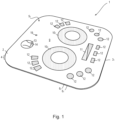
- Figure 1 shows a capacitive touch device 1 in the form of a vinyl record sleeve insert.
- the capacitive touch device 1 is pairable with a Bluetooth (RTM) enabled mobile device, such as a smart phone, and can be used to provide input signals for controlling the mobile device as described, for example, in WO 2013 117917 A2 .
- RTM Bluetooth
- the insert 1 comprises a single sheet 2 (best seen in Figure 5 ) of card which is folded in on itself along first and second fold lines 3 1 , 3 2 (best seen in Figure 5 ) to form a laminate structure 4 (best shown in Figure 1 ).
- Paper or card can be used having a weight of, for example, about 100 to about 200 g/m 2 . Heavier paper or card or even cardboard can be used, for example, having a weight of up to 350 g/m 2 or more.
- the sheet 1 has first and second faces 5 1 , 5 2 and the first fold line 3 1 separates first and second wings 6 1 , 6 2 .
- the second fold line 3 2 separates the first wing 6 1 and a wing extension 6 3 (herein also referred to as a "flap").
- the sheet 2 has first and second ends 7 1 , 7 2 and first and second edges 8 1 , 8 2 .
- the second (outward) face 5 2 of the second wing 6 2 supports printed indicia 9.
- the printed indicia 9 include an image of a DJ mixing desk including images of first and second turntables 10 1 , 10 2 , a crossover slider 11 and other buttons 12.
- the second wing 6 2 includes a tongue-shaped flap 13 held down by a transparent sticker 14.
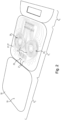
- the sticker 14 can be peeled off the area surrounding the flap 13 or entirely removed to allow the flap 13 to be lifted and access a coin cell 15 held in a holder 16 mounted on a circuit board 17 which also supports a microcontroller 18 providing Bluetooth (RTM) wireless connectivity. After the cell 15 has been replaced, the user can reapply or re-stick the sticker 14 or a new sticker (not shown).
- RTM Bluetooth
- the second wing 6 2 also includes a through-hole 19 which allows ambient light to pass to a photodiode 20 on the circuit board 17. This can be used to pass a signal (not shown) to the microcontroller 18 to switch the microcontroller 18 into a power-saving mode.
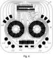
- the first face 5 1 of the first wing 6 1 supports a plurality of electrically-conductive pads 21 for providing capacitive touch switches, an array of electrically-conductive pads 22 for providing contact lands for contact pads 23 ( Figure 6 ) on the circuit board 17 and electrically-conductive tracks 24 interconnecting conductive pads 21, 22.
- the conductive pads 21, 22 and tracks 24 comprise carbon-based conductive ink formed by printing, for example, by lithographic or ink-jet printing process.
- Each conductive switch 21 has a surface area which is sufficiently large (e.g. > 0.2 cm 2 ) to provide a capacitive touch pad.
- Each conductive pad 22 has an area which is sufficiently large to provide electrical capacitive or resistive contact to a contact pad 23 ( Figure 6 ) on the circuit board 17 ( Figure 6 ).
- Some of the conductive switches 21 are arranged in an annular array to provide first and second capacitive touch wheels 25 1 , 25 2 .
- Other conductive switches 21 are arranged in a linear array to provide a capacitive touch slider 26.
- Other conductive switches 21 provide simple capacitive touch buttons 27.
- the printed indicia 9 and the conductive switches 21 are positioned so that, when the second wing 6 2 is folded over onto the first wing 6 1 , the images of first and second turntables 10 1 , 10 2 , crossover slider 11 and other buttons 12 are aligned with corresponding capacitive touch wheels 25 1 , 25 2 , capacitive touch slider 26 and capacitive touch buttons 27 ⁇ .
- the conductive tracks 24 have a width, w, which is sufficiently small (e.g. ⁇ 1 mm) so as to reduce capacitive coupling with a finger.
- a conductive track 24 may include a section 28 having a ladder-shaped arrangement as described, for example, in WO 2012 101448 A2 which can be used to help to reduce capacitance per unit length of a track 24 without significantly reducing its conductivity.
- the first face 5 1 of the sheet 2 which includes the conductive pads 21, 22, the conductive tracks 24 and unprinted areas 28, is coated with adhesive 29.
- the adhesive 29 is covered by a backing layer 30 which can be peeled away to reveal the adhesive 29.
- the adhesive 29 need not applied across all of the first face 5 1 of the sheet 2.
- adhesive 29 may be applied in selected areas including, for example, on just the first or second wing 6 1 , 6 2 and/or around the edges of the wing(s) 6 1 , 6 2 .
- An adhesive 29 need not be applied prior to assembly.
- the adhesive 29 can be applied during assembly.
- the adhesive 29 can be applied to the required areas by spraying an aerosol-based adhesive, using an adhesive stick, painting or printing liquid-based adhesive or by applying adhesive tape.
- the adhesive 29 may be one which is curable, for example, using heat or UV light.
- the touch slider 26 is supported directly on the first face 5 1 of sheet 2 and includes, among others, first, second, third, fourth, fifth and sixth co-planar capacitive touch switches 21 1 , 21 2 , 21 3 , 21 4 , 21 5 , 21 6 in a row.
- Conductive tracks 24 1 , 24 2 , 24 3 , 24 4 are also supported directly on the first face 5 1 of the sheet 2, i.e. on the same face as the capacitive touch switches 21 1 , 21 2 , 21 3 , 21 4 , 21 5 , 21 6 .
- a first conductive track 24 1 interconnects first and fifth capacitive touch switches 21 1 , 21 5 .
- a second conductive track 24 2 interconnects second and sixth capacitive touch switches 21 2 , 21 6 .
- Third and fourth conductive tracks 24 3 , 24 4 are connected to the third and fourth capacitive touch switches 21 3 , 21 4 respectively.
- the third and fourth capacitive touch switches 21 3 , 21 4 are adjacent and are electrically isolated from each other.
- the third and fourth capacitive touch switches 21 3 , 21 4 are separated by a channel 31 having a width w c .
- the first and fifth capacitive touch switches 21 1 , 21 5 are electrically isolated from the third and fourth capacitive touch switches 21 3 , 21 4 . However, the first conductive track 24 1 , which interconnects the two switches 21 1 , 21 5 , runs through the channel 31.
- second and sixth capacitive touch switches 21 2 , 21 6 are electrically isolated from the third and fourth capacitive touch switches 21 3 , 21 4 and the second conductive track 24 2 , which interconnects the two switches 21 2 , 21 6 , runs through the channel 31.
- the first and second conductive tracks 24 1 , 24 2 have a width w t .
- the channel width w c is at least three times, preferably at least five times, the track width w t .
- the tracks 24 1 , 24 2 are about 0.1 mm to 0.5 mm thick in the channel 31.
- the user can activate the third and fourth capacitive touch pad 21 3 , 21 4 , but not the other pads 21 1 , 21 2 , 21 5 , 21 6 while the finger is over the channel 31.
- the microcontroller 18 ( Figure 5 ) provides, among other functions, a capacitive touch controller.
- the microcontroller 18 is programmed to have a sensing threshold 32 selected such that, in response to a user's finger being directly over a capacitive touch pad 21 it has a signal level 33 which exceeds the threshold level 32 and generates a trigger signal (not shown) indicating that the capacitive touch switch 21 has been "pressed" (i.e. activated), but when a user's finger is over a conductive track 24, the measured signal level 34 falls below the threshold level 32 and so no trigger signal is generated.
- a similar arrangement is used for the conductive touch wheels 25 1 , 25 2 .
- a second fold line 3 2 separates the first wing 6 1 and a wing extension 6 3 .
- the wing extension 6 3 has a frame portion 35 which defines an aperture 36.
- the aperture 36 is dimensioned to accommodate the circuit board 17 and is positioned so that when the wing extension 6 3 is folded over onto the first wing 61 is creates a shallow cavity over the contact lands 22.
- the wing extension 6 3 can be replaced by or augmented by a separate sheet having an aperture. In some cases, the wing extension 6 3 can be omitted.
- the contact land 22 and corresponding contact pad 23 can be coupled capacitively as described, for example, in WO 2014 096772 A1 .
- the contact land 22 and corresponding contact pad 23 can be coupled resistively as described, for example, in PCT/GB2014/052832 .
- the adhesive 29 preferably should have a sheet resistance R S of at least 0.5 M ⁇ /sq.
- adhesive 29 may be applied to selective areas of the sheet. If the adhesive 29 is non conductive, then it can be omitted in the region over the contact lands 22. Alternatively, an adhesive 29 which is conductive may be used in which case it may be applied in a dot pattern as described in WO 2013 128198 A2 .
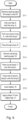
- the device 1 can be assembling by removing the backing paper 30 (or applying an adhesive 29 on the first face 5 1 of the sheet 2), folding over the wing extension 6 3 onto the first wing 6 2 , placing the circuit board 17 onto the contact lands 22 on the sheet 2 and then folding the second wing 62 onto the first wing 6 1 .
- the backing paper 30 is removed except in area 39 on the second wing 6 2 (step S1-1).
- the flap 63 is folded and stuck onto the first wing 6 1 (step S1-2).
- the second wing 6 2 is then folded over (step S1-3).
- the partially assembled device 1' can be run through a press 41 (step S1-4).
- the remaining backing paper 30 can be removed (step S1-5) and the circuit board 17 can be placed onto the first wing (step S1-6).
- the circuit board 17 can be placed with or without the battery 18 in place.
- the rest of the second wing 6 2 is folded over (step S1-7). If not already in place, the battery 18 is inserted (step S1-8).
- the sticker 14 is applied to the flap 13 (step S1-9).
- the process is similar to that described earlier with reference to Figure 9 .
- the whole device, including circuit board is passed through the press 41. This may be used particularly when the sheet is at least as thick as the circuit board 17 and any components supported on the board 17, or where an additional spacer insert is used and so the board or components are not subjected to the pressure of the press 41.
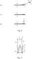
- Figure 11 shows the coin cell cover flap 13 is open so as to reveal the coin cell holder 16.
- the flap 13 and the corresponding aperture 42 formed in the sheet 2 may have inwardly-concave arcuate edges 43 1 , 43 2 , 43 3 .
- the arcuate edges 43 1 , 43 2 , 43 3 in the sheet 2 form spaces 44 1 , 44 2 which allow a tool (not shown) to access the coin cell holder 16 and allow it to push out the cell 15 out.
- the flap is formed by cutting slits in the sheet 2 and so is unitary with the rest of the sheet.
- the article need not be a vinyl record insert.
- the article may be a pamphlet, flyer, leaflet or other single sheet article.
- the printed article may be a promotional item.
- the printed article may be a map or a cover for a map.
- the printed article may be postcard or greetings card.
- the printed article may be a map or a cover for a map.
- the printed article may be an insert for another item, such as a magazine, book or other product.
- the printed article may be an insert in or part of product packaging.
- the product may be media (such as a vinyl record or a CD).
- the product may be an article of clothing, game or food stuff (such as box of cereal).
- the insert may be free or bound into another item.
- the printed article may be a game or playing card.
- the printed article may be a point-of-sale display.
- the device may include three, four, five or more wings.
- the wings need not be all the same size.
- fold lines need not all be parallel.
- one or more fold lines may be perpendicular to another fold line.
- a device may be assembled from a 'L'-shaped, 'T'-shaped, '+'-shaped or other, more complex layouts.
- the printed article may include other forms of output device, such as piezoelectric buzzer or other sound-emitting device, and/or one or more light-emitting diodes or other light-emitting or display device(s).
- output device such as piezoelectric buzzer or other sound-emitting device, and/or one or more light-emitting diodes or other light-emitting or display device(s).
Landscapes
- Engineering & Computer Science (AREA)
- General Engineering & Computer Science (AREA)
- Theoretical Computer Science (AREA)
- Human Computer Interaction (AREA)
- Physics & Mathematics (AREA)
- General Physics & Mathematics (AREA)
- Microelectronics & Electronic Packaging (AREA)
- Mechanical Engineering (AREA)
- Switches That Are Operated By Magnetic Or Electric Fields (AREA)
Claims (9)
- Dispositif tactile capacitif comprenant :un substrat (2) ; etune pluralité de commutateurs tactiles capacitifs coplanaires (211, 212, 213, 214, 215, 216) et de pistes conductrices (241, 242, 243, 244) raccordées aux commutateurs tactiles capacitifs disposés directement sur une face du substrat, les commutateurs tactiles capacitifs comprenant :des premier et deuxième commutateurs tactiles capacitifs (213, 214) qui sont adjacents, séparés par un canal (31) possédant une largeur de canal wc, et qui sont isolés électriquement l'un de l'autre ; etdes troisième et quatrième commutateurs tactiles capacitifs (212, 216) qui sont isolés électriquement des premier et deuxième commutateurs tactiles capacitifs, mais qui sont électriquement raccordés l'un à l'autre par une piste conductrice (242) possédant une largeur de piste wt qui traverse le canal,caractérisé en ce que la largeur de canal wc est au moins trois fois la largeur de piste wt ; et en ce que la largeur de piste wt est comprise entre 0,1 mm et 0,5 mm.
- Dispositif tactile capacitif selon la revendication 1, ladite piste conductrice étant une première piste conductrice et lesdits commutateurs tactiles capacitifs comprenant en outre :
des cinquième et sixième commutateurs tactiles capacitifs qui sont électriquement isolés des premier, deuxième, troisième et quatrième commutateurs tactiles capacitifs, mais qui sont électriquement raccordés l'un à l'autre par une deuxième piste conductrice qui traverse le canal. - Dispositif tactile capacitif selon une quelconque revendication précédente, lesdits commutateurs tactiles capacitifs et lesdites pistes conductrices comprenant une encre conductrice, telle qu'une encre conductrice à base de carbone.
- Dispositif tactile capacitif selon une quelconque revendication précédente, comprenant en outre des plages de contact, les pistes conductrices raccordant les commutateurs tactiles et les plages de contact.
- Dispositif tactile capacitif selon une quelconque revendication précédente, ledit substrat comprenant un matériau à base de fibres, tel que du carton.
- Dispositif tactile capacitif selon une quelconque revendication précédente, lesdits commutateurs tactiles capacitifs étant agencés pour fournir un curseur tactile capacitif.
- Dispositif tactile capacitif selon une quelconque revendication précédente, lesdits commutateurs tactiles capacitifs étant agencés pour fournir une molette tactile capacitive.
- Dispositif tactile capacitif selon une quelconque revendication précédente, comprenant en outre : un dispositif de commande tactile capacitif couplé aux commutateurs tactiles capacitifs configuré pour posséder un seuil de détection sélectionné de sorte que, en réponse au doigt d'un utilisateur passant sur les premier et deuxième commutateurs tactiles capacitifs mais pas les troisième ou quatrième commutateurs tactiles capacitifs, le dispositif de commande génère des déclencheurs respectifs pour les premier et deuxième commutateurs tactiles, mais pas de déclencheurs pour les troisième ou quatrième commutateurs tactiles capacitifs.
- Dispositif tactile capacitif selon une quelconque revendication précédente, qui est un article imprimé.
Applications Claiming Priority (2)
| Application Number | Priority Date | Filing Date | Title |
|---|---|---|---|
| GB1418443.6A GB2523216B (en) | 2014-10-17 | 2014-10-17 | Capacitive touch device |
| PCT/GB2015/053059 WO2016059414A1 (fr) | 2014-10-17 | 2015-10-15 | Dispositif tactile capacitif |
Publications (2)
| Publication Number | Publication Date |
|---|---|
| EP3207441A1 EP3207441A1 (fr) | 2017-08-23 |
| EP3207441B1 true EP3207441B1 (fr) | 2023-03-01 |
Family
ID=52013143
Family Applications (1)
| Application Number | Title | Priority Date | Filing Date |
|---|---|---|---|
| EP15784123.0A Active EP3207441B1 (fr) | 2014-10-17 | 2015-10-15 | Dispositif tactile capacitif |
Country Status (5)
| Country | Link |
|---|---|
| US (1) | US10389355B2 (fr) |
| EP (1) | EP3207441B1 (fr) |
| CN (1) | CN107077223A (fr) |
| GB (1) | GB2523216B (fr) |
| WO (1) | WO2016059414A1 (fr) |
Families Citing this family (10)
| Publication number | Priority date | Publication date | Assignee | Title |
|---|---|---|---|---|
| GB2531703B (en) * | 2014-10-17 | 2017-07-19 | Novalia Ltd | Printed article |
| US20180317314A1 (en) * | 2015-10-23 | 2018-11-01 | Universität des Saarlandes | Object Made of a Folded Sheet with Printed Electric Controls |
| US10527487B2 (en) | 2016-05-31 | 2020-01-07 | Future Technologies In Sport, Inc. | System and method for sensing high-frequency vibrations on sporting equipment |
| US10530083B2 (en) | 2016-11-16 | 2020-01-07 | Honeywell Safety Products Usa, Inc. | Printed circuit board biosensing garment connector |
| JP6997874B2 (ja) * | 2017-09-25 | 2022-01-18 | メリット オートモーティヴ エレクトロニクス システムズ エス.エル.ユー | 内部キャリアシートを備えた静電容量式タッチパネルユニット |
| JP7071234B2 (ja) * | 2018-06-29 | 2022-05-18 | キヤノン株式会社 | 電子機器 |
| US11711892B2 (en) * | 2019-07-15 | 2023-07-25 | Velvetwire Llc | Method of manufacture and use of a flexible computerized sensing device |
| CN115003023A (zh) * | 2022-05-26 | 2022-09-02 | 意力(广州)电子科技有限公司 | 电容按键电路板 |
| IT202200026856A1 (it) * | 2022-12-27 | 2024-06-27 | Carel Ind Spa | Interfaccia per controllore e processo di assemblaggio della stessa |
| GB2626014B (en) | 2023-01-06 | 2025-04-30 | Mocanu Calin | A system of robots and robotic parts including method of construction and method of use |
Citations (1)
| Publication number | Priority date | Publication date | Assignee | Title |
|---|---|---|---|---|
| GB2487579A (en) * | 2011-01-28 | 2012-08-01 | Novalia Ltd | Composite conductive element and connecting conductor for capacitive touch sensor |
Family Cites Families (43)
| Publication number | Priority date | Publication date | Assignee | Title |
|---|---|---|---|---|
| US4096577A (en) * | 1975-03-03 | 1978-06-20 | Ferber Leon A | Thin flexible electronic calculator |
| US6869208B2 (en) | 2001-01-02 | 2005-03-22 | Vogel Applied Technologies | Illuminated animated ornament |
| JP3971907B2 (ja) | 2001-09-17 | 2007-09-05 | アルプス電気株式会社 | 座標入力装置及び電子機器 |
| US20030192209A1 (en) | 2002-04-15 | 2003-10-16 | Ming-Yuan Yeh | Electroluminescent lamp-based greeting cards |
| US7477242B2 (en) * | 2002-05-20 | 2009-01-13 | 3M Innovative Properties Company | Capacitive touch screen with conductive polymer |
| US6845583B2 (en) | 2003-05-28 | 2005-01-25 | Lux Imports, Inc. | Audio/visual greeting device |
| GB2429111A (en) * | 2005-08-10 | 2007-02-14 | Nicholas Jim Stone | Electronic tag |
| WO2008082616A1 (fr) | 2006-12-29 | 2008-07-10 | Solicore, Inc. | Carte conçue pour recevoir une batterie séparée |
| US7736891B2 (en) | 2007-09-11 | 2010-06-15 | University Of Washington | Microfluidic assay system with dispersion monitoring |
| US8719033B2 (en) | 2008-04-11 | 2014-05-06 | Hallmark Cards, Incorporated | Greeting card having karaoke record feature and simultaneous playback |
| GB2459265B (en) | 2008-04-15 | 2012-08-08 | Novalia Ltd | Printed article |
| US8629841B2 (en) | 2008-04-30 | 2014-01-14 | Apple Inc. | Multi-touch sensor patterns and stack-ups |
| US20090314550A1 (en) | 2008-06-18 | 2009-12-24 | Layton Michael D | Touchpad designed in a planar configuration that can be molded to conform to a non-planar object |
| US7630203B1 (en) | 2008-09-17 | 2009-12-08 | Ardi Technology Corporation | IC card |
| DE202008012847U1 (de) | 2008-09-26 | 2008-12-11 | ARDI TECHNOLOGY CORPORATION, Tucheng City | IC-Karte mit auswechselbarer Batterie |
| US8982051B2 (en) | 2009-03-30 | 2015-03-17 | Microsoft Technology Licensing, Llc | Detecting touch on a surface |
| JP2010244772A (ja) | 2009-04-03 | 2010-10-28 | Sony Corp | 静電容量式タッチ部材及びその製造方法、並びに静電容量式タッチ検出装置 |
| GB2475253A (en) * | 2009-11-11 | 2011-05-18 | Novalia Ltd | A sheet with capacitive elements for input |
| DE112011101362T5 (de) * | 2010-04-19 | 2013-01-31 | Methode Electronics, Inc. | Multifunktionssensor und Verfahren |
| EP2569645A4 (fr) | 2010-05-10 | 2014-09-24 | Pure Imagination Llc | Détecteurs tactiles capacitifs à film mince à une face |
| AU2014202373B2 (en) | 2010-05-10 | 2015-04-30 | Pure Imagination Llc | One sided thin film capacitive touch sensors |
| US8947399B2 (en) | 2010-05-11 | 2015-02-03 | Tpk Touch Solutions Inc. | Dual-substrate capacitive touch panel |
| CN102402895A (zh) | 2010-09-17 | 2012-04-04 | 深圳市普天文科技有限公司 | 一种电容式触摸发声地球仪 |
| GB2487580A (en) | 2011-01-28 | 2012-08-01 | Novalia Ltd | Sheet for user interface with capacitive sensing elements |
| JP5436485B2 (ja) * | 2011-03-30 | 2014-03-05 | アルプス電気株式会社 | 入力装置 |
| DE102011111506B4 (de) | 2011-08-31 | 2017-05-18 | Leonhard Kurz Stiftung & Co. Kg | Kunststofffolie und Touchsensor |
| JP2013058117A (ja) | 2011-09-09 | 2013-03-28 | Alps Electric Co Ltd | 入力装置 |
| WO2013063445A2 (fr) * | 2011-10-28 | 2013-05-02 | President And Fellows Of Harvard College | Accéléromètres et capteurs tactiles basé sur de papier, capacitifs |
| US8710854B2 (en) | 2011-11-29 | 2014-04-29 | Eastman Kodak Company | Making transparent capacitor with multi-layer grid |
| GB2499987B (en) | 2012-03-02 | 2017-01-11 | Novalia Ltd | Touch-sensitive input device |
| US9239655B2 (en) | 2012-05-10 | 2016-01-19 | Nuvoton Technology Corporation | Parsimonious systems for touch detection and capacitive touch methods useful in conjunction therewith |
| CN103389844B (zh) * | 2012-05-10 | 2016-09-07 | 新唐科技股份有限公司 | 触控检测系统及其电容式触控检测方法 |
| KR101339692B1 (ko) | 2012-05-25 | 2013-12-10 | 크루셜텍 (주) | 그룹 식별을 이용한 터치 감지 장치 및 방법 |
| TWI463374B (zh) * | 2012-06-07 | 2014-12-01 | Mstar Semiconductor Inc | 觸控面板 |
| JP5850804B2 (ja) | 2012-06-19 | 2016-02-03 | 日本写真印刷株式会社 | タッチパネル、タッチパネルの製造方法 |
| US9354703B2 (en) | 2012-06-26 | 2016-05-31 | Fondazione Istituto Italiano Di Tecnologia | Tactile control arrangement for electrical or electronic devices integrated in a textile support |
| FI126349B (en) | 2012-12-31 | 2016-10-14 | Suunto Oy | Electronic device case |
| US9350344B2 (en) * | 2013-03-15 | 2016-05-24 | Pure Imagination, LLC | Test pattern membrane and method for testing capacitive sensors |
| KR101452302B1 (ko) | 2013-07-29 | 2014-10-22 | 주식회사 하이딥 | 터치 센서 패널 |
| KR102230300B1 (ko) | 2014-04-08 | 2021-03-22 | 삼성디스플레이 주식회사 | 지구본 표시장치 |
| GB2531339B (en) | 2014-10-17 | 2018-03-21 | Novalia Ltd | Capacitive touch device |
| GB2531703B (en) | 2014-10-17 | 2017-07-19 | Novalia Ltd | Printed article |
| GB2531607B (en) | 2014-10-24 | 2018-04-18 | Novalia Ltd | Article incorporating a capacitive touch device and having a non-flat surface |
-
2014
- 2014-10-17 GB GB1418443.6A patent/GB2523216B/en active Active
-
2015
- 2015-10-15 EP EP15784123.0A patent/EP3207441B1/fr active Active
- 2015-10-15 US US15/519,337 patent/US10389355B2/en active Active
- 2015-10-15 CN CN201580056382.2A patent/CN107077223A/zh active Pending
- 2015-10-15 WO PCT/GB2015/053059 patent/WO2016059414A1/fr not_active Ceased
Patent Citations (1)
| Publication number | Priority date | Publication date | Assignee | Title |
|---|---|---|---|---|
| GB2487579A (en) * | 2011-01-28 | 2012-08-01 | Novalia Ltd | Composite conductive element and connecting conductor for capacitive touch sensor |
Also Published As
| Publication number | Publication date |
|---|---|
| WO2016059414A1 (fr) | 2016-04-21 |
| GB2523216B (en) | 2016-01-27 |
| GB201418443D0 (en) | 2014-12-03 |
| EP3207441A1 (fr) | 2017-08-23 |
| CN107077223A (zh) | 2017-08-18 |
| GB2523216A (en) | 2015-08-19 |
| US10389355B2 (en) | 2019-08-20 |
| US20170237430A1 (en) | 2017-08-17 |
Similar Documents
| Publication | Publication Date | Title |
|---|---|---|
| EP3207441B1 (fr) | Dispositif tactile capacitif | |
| EP3206883B1 (fr) | Dispositif tactile capacitif | |
| JP5986109B2 (ja) | 導電性要素 | |
| KR101651609B1 (ko) | 평면 데이터 캐리어 | |
| US9489856B2 (en) | Interactive printed article with touch-activated presentation | |
| US20170153153A1 (en) | Metalized polyester film force sensors | |
| EP2303592B1 (fr) | Livre | |
| CN102971155A (zh) | 电子装置 | |
| EP3206882B1 (fr) | Article imprimé | |
| EP2936683B1 (fr) | Dispositif tactile capacitif | |
| CN103338941B (zh) | 书 | |
| EP3047708B1 (fr) | Ensemble carte à circuit imprimé | |
| WO2017037412A1 (fr) | Article imprimé à fonction tactile capacitive | |
| GB2462287A (en) | Printed touch switch | |
| GB2531605A (en) | Capacitive Touch Device |
Legal Events
| Date | Code | Title | Description |
|---|---|---|---|
| STAA | Information on the status of an ep patent application or granted ep patent |
Free format text: STATUS: THE INTERNATIONAL PUBLICATION HAS BEEN MADE |
|
| PUAI | Public reference made under article 153(3) epc to a published international application that has entered the european phase |
Free format text: ORIGINAL CODE: 0009012 |
|
| STAA | Information on the status of an ep patent application or granted ep patent |
Free format text: STATUS: REQUEST FOR EXAMINATION WAS MADE |
|
| 17P | Request for examination filed |
Effective date: 20170508 |
|
| AK | Designated contracting states |
Kind code of ref document: A1 Designated state(s): AL AT BE BG CH CY CZ DE DK EE ES FI FR GB GR HR HU IE IS IT LI LT LU LV MC MK MT NL NO PL PT RO RS SE SI SK SM TR |
|
| AX | Request for extension of the european patent |
Extension state: BA ME |
|
| DAV | Request for validation of the european patent (deleted) | ||
| DAX | Request for extension of the european patent (deleted) | ||
| STAA | Information on the status of an ep patent application or granted ep patent |
Free format text: STATUS: EXAMINATION IS IN PROGRESS |
|
| 17Q | First examination report despatched |
Effective date: 20201030 |
|
| REG | Reference to a national code |
Ref country code: DE Ref legal event code: R079 Ref document number: 602015082657 Country of ref document: DE Free format text: PREVIOUS MAIN CLASS: G06F0003044000 Ipc: H05K0001140000 |
|
| GRAP | Despatch of communication of intention to grant a patent |
Free format text: ORIGINAL CODE: EPIDOSNIGR1 |
|
| STAA | Information on the status of an ep patent application or granted ep patent |
Free format text: STATUS: GRANT OF PATENT IS INTENDED |
|
| RIC1 | Information provided on ipc code assigned before grant |
Ipc: H03K 17/96 20060101ALI20220829BHEP Ipc: G06F 3/023 20060101ALI20220829BHEP Ipc: G06F 3/02 20060101ALI20220829BHEP Ipc: H05K 3/36 20060101ALI20220829BHEP Ipc: H05K 1/16 20060101ALI20220829BHEP Ipc: H05K 1/14 20060101AFI20220829BHEP |
|
| INTG | Intention to grant announced |
Effective date: 20220920 |
|
| GRAS | Grant fee paid |
Free format text: ORIGINAL CODE: EPIDOSNIGR3 |
|
| GRAA | (expected) grant |
Free format text: ORIGINAL CODE: 0009210 |
|
| STAA | Information on the status of an ep patent application or granted ep patent |
Free format text: STATUS: THE PATENT HAS BEEN GRANTED |
|
| AK | Designated contracting states |
Kind code of ref document: B1 Designated state(s): AL AT BE BG CH CY CZ DE DK EE ES FI FR GB GR HR HU IE IS IT LI LT LU LV MC MK MT NL NO PL PT RO RS SE SI SK SM TR |
|
| REG | Reference to a national code |
Ref country code: GB Ref legal event code: FG4D |
|
| REG | Reference to a national code |
Ref country code: CH Ref legal event code: EP Ref country code: AT Ref legal event code: REF Ref document number: 1551931 Country of ref document: AT Kind code of ref document: T Effective date: 20230315 |
|
| REG | Reference to a national code |
Ref country code: DE Ref legal event code: R096 Ref document number: 602015082657 Country of ref document: DE |
|
| REG | Reference to a national code |
Ref country code: IE Ref legal event code: FG4D |
|
| REG | Reference to a national code |
Ref country code: LT Ref legal event code: MG9D |
|
| REG | Reference to a national code |
Ref country code: NL Ref legal event code: MP Effective date: 20230301 |
|
| PG25 | Lapsed in a contracting state [announced via postgrant information from national office to epo] |
Ref country code: RS Free format text: LAPSE BECAUSE OF FAILURE TO SUBMIT A TRANSLATION OF THE DESCRIPTION OR TO PAY THE FEE WITHIN THE PRESCRIBED TIME-LIMIT Effective date: 20230301 Ref country code: NO Free format text: LAPSE BECAUSE OF FAILURE TO SUBMIT A TRANSLATION OF THE DESCRIPTION OR TO PAY THE FEE WITHIN THE PRESCRIBED TIME-LIMIT Effective date: 20230601 Ref country code: LV Free format text: LAPSE BECAUSE OF FAILURE TO SUBMIT A TRANSLATION OF THE DESCRIPTION OR TO PAY THE FEE WITHIN THE PRESCRIBED TIME-LIMIT Effective date: 20230301 Ref country code: LT Free format text: LAPSE BECAUSE OF FAILURE TO SUBMIT A TRANSLATION OF THE DESCRIPTION OR TO PAY THE FEE WITHIN THE PRESCRIBED TIME-LIMIT Effective date: 20230301 Ref country code: HR Free format text: LAPSE BECAUSE OF FAILURE TO SUBMIT A TRANSLATION OF THE DESCRIPTION OR TO PAY THE FEE WITHIN THE PRESCRIBED TIME-LIMIT Effective date: 20230301 Ref country code: ES Free format text: LAPSE BECAUSE OF FAILURE TO SUBMIT A TRANSLATION OF THE DESCRIPTION OR TO PAY THE FEE WITHIN THE PRESCRIBED TIME-LIMIT Effective date: 20230301 |
|
| REG | Reference to a national code |
Ref country code: AT Ref legal event code: MK05 Ref document number: 1551931 Country of ref document: AT Kind code of ref document: T Effective date: 20230301 |
|
| PG25 | Lapsed in a contracting state [announced via postgrant information from national office to epo] |
Ref country code: SE Free format text: LAPSE BECAUSE OF FAILURE TO SUBMIT A TRANSLATION OF THE DESCRIPTION OR TO PAY THE FEE WITHIN THE PRESCRIBED TIME-LIMIT Effective date: 20230301 Ref country code: PL Free format text: LAPSE BECAUSE OF FAILURE TO SUBMIT A TRANSLATION OF THE DESCRIPTION OR TO PAY THE FEE WITHIN THE PRESCRIBED TIME-LIMIT Effective date: 20230301 Ref country code: NL Free format text: LAPSE BECAUSE OF FAILURE TO SUBMIT A TRANSLATION OF THE DESCRIPTION OR TO PAY THE FEE WITHIN THE PRESCRIBED TIME-LIMIT Effective date: 20230301 Ref country code: GR Free format text: LAPSE BECAUSE OF FAILURE TO SUBMIT A TRANSLATION OF THE DESCRIPTION OR TO PAY THE FEE WITHIN THE PRESCRIBED TIME-LIMIT Effective date: 20230602 Ref country code: FI Free format text: LAPSE BECAUSE OF FAILURE TO SUBMIT A TRANSLATION OF THE DESCRIPTION OR TO PAY THE FEE WITHIN THE PRESCRIBED TIME-LIMIT Effective date: 20230301 |
|
| PG25 | Lapsed in a contracting state [announced via postgrant information from national office to epo] |
Ref country code: SM Free format text: LAPSE BECAUSE OF FAILURE TO SUBMIT A TRANSLATION OF THE DESCRIPTION OR TO PAY THE FEE WITHIN THE PRESCRIBED TIME-LIMIT Effective date: 20230301 Ref country code: RO Free format text: LAPSE BECAUSE OF FAILURE TO SUBMIT A TRANSLATION OF THE DESCRIPTION OR TO PAY THE FEE WITHIN THE PRESCRIBED TIME-LIMIT Effective date: 20230301 Ref country code: PT Free format text: LAPSE BECAUSE OF FAILURE TO SUBMIT A TRANSLATION OF THE DESCRIPTION OR TO PAY THE FEE WITHIN THE PRESCRIBED TIME-LIMIT Effective date: 20230703 Ref country code: EE Free format text: LAPSE BECAUSE OF FAILURE TO SUBMIT A TRANSLATION OF THE DESCRIPTION OR TO PAY THE FEE WITHIN THE PRESCRIBED TIME-LIMIT Effective date: 20230301 Ref country code: CZ Free format text: LAPSE BECAUSE OF FAILURE TO SUBMIT A TRANSLATION OF THE DESCRIPTION OR TO PAY THE FEE WITHIN THE PRESCRIBED TIME-LIMIT Effective date: 20230301 Ref country code: AT Free format text: LAPSE BECAUSE OF FAILURE TO SUBMIT A TRANSLATION OF THE DESCRIPTION OR TO PAY THE FEE WITHIN THE PRESCRIBED TIME-LIMIT Effective date: 20230301 |
|
| PG25 | Lapsed in a contracting state [announced via postgrant information from national office to epo] |
Ref country code: SK Free format text: LAPSE BECAUSE OF FAILURE TO SUBMIT A TRANSLATION OF THE DESCRIPTION OR TO PAY THE FEE WITHIN THE PRESCRIBED TIME-LIMIT Effective date: 20230301 Ref country code: IS Free format text: LAPSE BECAUSE OF FAILURE TO SUBMIT A TRANSLATION OF THE DESCRIPTION OR TO PAY THE FEE WITHIN THE PRESCRIBED TIME-LIMIT Effective date: 20230701 |
|
| REG | Reference to a national code |
Ref country code: DE Ref legal event code: R097 Ref document number: 602015082657 Country of ref document: DE |
|
| PLBE | No opposition filed within time limit |
Free format text: ORIGINAL CODE: 0009261 |
|
| STAA | Information on the status of an ep patent application or granted ep patent |
Free format text: STATUS: NO OPPOSITION FILED WITHIN TIME LIMIT |
|
| PG25 | Lapsed in a contracting state [announced via postgrant information from national office to epo] |
Ref country code: SI Free format text: LAPSE BECAUSE OF FAILURE TO SUBMIT A TRANSLATION OF THE DESCRIPTION OR TO PAY THE FEE WITHIN THE PRESCRIBED TIME-LIMIT Effective date: 20230301 Ref country code: DK Free format text: LAPSE BECAUSE OF FAILURE TO SUBMIT A TRANSLATION OF THE DESCRIPTION OR TO PAY THE FEE WITHIN THE PRESCRIBED TIME-LIMIT Effective date: 20230301 |
|
| 26N | No opposition filed |
Effective date: 20231204 |
|
| PG25 | Lapsed in a contracting state [announced via postgrant information from national office to epo] |
Ref country code: IT Free format text: LAPSE BECAUSE OF FAILURE TO SUBMIT A TRANSLATION OF THE DESCRIPTION OR TO PAY THE FEE WITHIN THE PRESCRIBED TIME-LIMIT Effective date: 20230301 Ref country code: MC Free format text: LAPSE BECAUSE OF FAILURE TO SUBMIT A TRANSLATION OF THE DESCRIPTION OR TO PAY THE FEE WITHIN THE PRESCRIBED TIME-LIMIT Effective date: 20230301 |
|
| REG | Reference to a national code |
Ref country code: CH Ref legal event code: PL |
|
| REG | Reference to a national code |
Ref country code: BE Ref legal event code: MM Effective date: 20231031 |
|
| PG25 | Lapsed in a contracting state [announced via postgrant information from national office to epo] |
Ref country code: LU Free format text: LAPSE BECAUSE OF NON-PAYMENT OF DUE FEES Effective date: 20231015 |
|
| PG25 | Lapsed in a contracting state [announced via postgrant information from national office to epo] |
Ref country code: LU Free format text: LAPSE BECAUSE OF NON-PAYMENT OF DUE FEES Effective date: 20231015 |
|
| PG25 | Lapsed in a contracting state [announced via postgrant information from national office to epo] |
Ref country code: CH Free format text: LAPSE BECAUSE OF NON-PAYMENT OF DUE FEES Effective date: 20231031 |
|
| PG25 | Lapsed in a contracting state [announced via postgrant information from national office to epo] |
Ref country code: CH Free format text: LAPSE BECAUSE OF NON-PAYMENT OF DUE FEES Effective date: 20231031 |
|
| PG25 | Lapsed in a contracting state [announced via postgrant information from national office to epo] |
Ref country code: BE Free format text: LAPSE BECAUSE OF NON-PAYMENT OF DUE FEES Effective date: 20231031 |
|
| PG25 | Lapsed in a contracting state [announced via postgrant information from national office to epo] |
Ref country code: IE Free format text: LAPSE BECAUSE OF NON-PAYMENT OF DUE FEES Effective date: 20231015 |
|
| PG25 | Lapsed in a contracting state [announced via postgrant information from national office to epo] |
Ref country code: IE Free format text: LAPSE BECAUSE OF NON-PAYMENT OF DUE FEES Effective date: 20231015 |
|
| PG25 | Lapsed in a contracting state [announced via postgrant information from national office to epo] |
Ref country code: BG Free format text: LAPSE BECAUSE OF FAILURE TO SUBMIT A TRANSLATION OF THE DESCRIPTION OR TO PAY THE FEE WITHIN THE PRESCRIBED TIME-LIMIT Effective date: 20230301 |
|
| PG25 | Lapsed in a contracting state [announced via postgrant information from national office to epo] |
Ref country code: BG Free format text: LAPSE BECAUSE OF FAILURE TO SUBMIT A TRANSLATION OF THE DESCRIPTION OR TO PAY THE FEE WITHIN THE PRESCRIBED TIME-LIMIT Effective date: 20230301 |
|
| PGFP | Annual fee paid to national office [announced via postgrant information from national office to epo] |
Ref country code: DE Payment date: 20241021 Year of fee payment: 10 |
|
| PGFP | Annual fee paid to national office [announced via postgrant information from national office to epo] |
Ref country code: FR Payment date: 20241030 Year of fee payment: 10 |
|
| PG25 | Lapsed in a contracting state [announced via postgrant information from national office to epo] |
Ref country code: CY Free format text: LAPSE BECAUSE OF FAILURE TO SUBMIT A TRANSLATION OF THE DESCRIPTION OR TO PAY THE FEE WITHIN THE PRESCRIBED TIME-LIMIT; INVALID AB INITIO Effective date: 20151015 |
|
| PG25 | Lapsed in a contracting state [announced via postgrant information from national office to epo] |
Ref country code: HU Free format text: LAPSE BECAUSE OF FAILURE TO SUBMIT A TRANSLATION OF THE DESCRIPTION OR TO PAY THE FEE WITHIN THE PRESCRIBED TIME-LIMIT; INVALID AB INITIO Effective date: 20151015 |
|
| PG25 | Lapsed in a contracting state [announced via postgrant information from national office to epo] |
Ref country code: TR Free format text: LAPSE BECAUSE OF FAILURE TO SUBMIT A TRANSLATION OF THE DESCRIPTION OR TO PAY THE FEE WITHIN THE PRESCRIBED TIME-LIMIT Effective date: 20230301 |
|
| REG | Reference to a national code |
Ref country code: GB Ref legal event code: 732E Free format text: REGISTERED BETWEEN 20260226 AND 20260304 |
|
| PGFP | Annual fee paid to national office [announced via postgrant information from national office to epo] |
Ref country code: GB Payment date: 20260331 Year of fee payment: 11 |