EP3207574B1 - Speicherzellen, halbleiterbauelemente und verfahren zur herstellung - Google Patents
Speicherzellen, halbleiterbauelemente und verfahren zur herstellung Download PDFInfo
- Publication number
- EP3207574B1 EP3207574B1 EP15851503.1A EP15851503A EP3207574B1 EP 3207574 B1 EP3207574 B1 EP 3207574B1 EP 15851503 A EP15851503 A EP 15851503A EP 3207574 B1 EP3207574 B1 EP 3207574B1
- Authority
- EP
- European Patent Office
- Prior art keywords
- precursor
- region
- getter
- species
- magnetic
- Prior art date
- Legal status (The legal status is an assumption and is not a legal conclusion. Google has not performed a legal analysis and makes no representation as to the accuracy of the status listed.)
- Active
Links
Images


Classifications
-
- H—ELECTRICITY
- H10—SEMICONDUCTOR DEVICES; ELECTRIC SOLID-STATE DEVICES NOT OTHERWISE PROVIDED FOR
- H10B—ELECTRONIC MEMORY DEVICES
- H10B61/00—Magnetic memory devices, e.g. magnetoresistive RAM [MRAM] devices
-
- H—ELECTRICITY
- H10—SEMICONDUCTOR DEVICES; ELECTRIC SOLID-STATE DEVICES NOT OTHERWISE PROVIDED FOR
- H10N—ELECTRIC SOLID-STATE DEVICES NOT OTHERWISE PROVIDED FOR
- H10N50/00—Galvanomagnetic devices
- H10N50/10—Magnetoresistive devices
-
- H—ELECTRICITY
- H10—SEMICONDUCTOR DEVICES; ELECTRIC SOLID-STATE DEVICES NOT OTHERWISE PROVIDED FOR
- H10B—ELECTRONIC MEMORY DEVICES
- H10B61/00—Magnetic memory devices, e.g. magnetoresistive RAM [MRAM] devices
- H10B61/20—Magnetic memory devices, e.g. magnetoresistive RAM [MRAM] devices comprising components having three or more electrodes, e.g. transistors
-
- H—ELECTRICITY
- H10—SEMICONDUCTOR DEVICES; ELECTRIC SOLID-STATE DEVICES NOT OTHERWISE PROVIDED FOR
- H10N—ELECTRIC SOLID-STATE DEVICES NOT OTHERWISE PROVIDED FOR
- H10N50/00—Galvanomagnetic devices
- H10N50/01—Manufacture or treatment
-
- H—ELECTRICITY
- H10—SEMICONDUCTOR DEVICES; ELECTRIC SOLID-STATE DEVICES NOT OTHERWISE PROVIDED FOR
- H10N—ELECTRIC SOLID-STATE DEVICES NOT OTHERWISE PROVIDED FOR
- H10N50/00—Galvanomagnetic devices
- H10N50/80—Constructional details
-
- H—ELECTRICITY
- H10—SEMICONDUCTOR DEVICES; ELECTRIC SOLID-STATE DEVICES NOT OTHERWISE PROVIDED FOR
- H10N—ELECTRIC SOLID-STATE DEVICES NOT OTHERWISE PROVIDED FOR
- H10N50/00—Galvanomagnetic devices
- H10N50/80—Constructional details
- H10N50/85—Materials of the active region
Definitions
- the present disclosure in various embodiments, relates generally to the field of memory device design and fabrication. More particularly, this disclosure relates to design and fabrication of memory cells characterized as spin torque transfer magnetic random access memory (STT-MRAM) cells, to semiconductor structures employed in such memory cells, and to semiconductor devices incorporating such memory cells.
- STT-MRAM spin torque transfer magnetic random access memory
- EP1885006A1 relates to capping layer for a magnetic tunnel junction device to enhance dR/R and a method of making the same.
- US8206742B2 relates to sustained release compositions of alfuzosin.
- Magnetic Random Access Memory is a non-volatile computer memory technology based on magnetoresistance.
- MRAM spin torque transfer MRAM
- a magnetic cell core includes a magnetic tunnel junction ("MTJ") sub-structure with at least two magnetic regions, for example, a "fixed region” and a "free region,” with a non-magnetic region between.
- the free region and the fixed region may exhibit magnetic orientations that are either horizontally oriented ("in-plane") or perpendicularly oriented (“out-of-plane”) relative to the width of the regions.
- the fixed region includes a magnetic material that has a substantially fixed (e.g., a non-switchable) magnetic orientation.
- the free region includes a magnetic material that has a magnetic orientation that may be switched, during operation of the cell, between a "parallel" configuration and an "anti-parallel” configuration.
- the magnetic orientations of the fixed region and the free region are directed in the same direction (e.g., north and north, east and east, south and south, or west and west, respectively).
- the magnetic orientations of the fixed region and the free region are directed in opposite directions (e.g., north and south, east and west, south and north, or west and east, respectively).
- the STT-MRAM cell In the parallel configuration, the STT-MRAM cell exhibits a lower electrical resistance across the magnetoresistive elements (e.g., the fixed region and free region), defining a "0" logic state of the MRAM cell. In the anti-parallel configuration, the STT-MRAM cell exhibits a higher electrical resistance across the magnetoresistive elements, defining a "1" logic state of the STT-MRAM cell.
- Switching of the magnetic orientation of the free region may be accomplished by passing a programming current through the magnetic cell core, including the fixed and free regions.
- the fixed region polarizes the electron spin of the programming current, and torque is created as the spin-polarized current passes through the core.
- the spin-polarized electron current exerts the torque on the free region.
- J c critical switching current density
- the programming current can be used to alter the electrical resistance across the magnetic regions.
- the resulting high or low electrical resistance states across the magnetoresistive elements enable the write and read operations of the MRAM cell.
- the magnetic orientation of the free region is usually desired to be maintained, during a "storage" stage, until the MRAM cell is to be rewritten to a different configuration (i.e., to a different logic state).
- Some STT-MRAM cells include dual oxide regions, i.e., another oxide region in addition to an "intermediate oxide region" (which may also be referred to as a "tunnel barrier") of the MTJ sub-structure.
- the free region may be between the intermediate oxide region and the another oxide region.
- the exposure of the free region to two oxide regions may increase the free region's magnetic anisotropy ("MA") strength as well as lower the damping in the cell core.
- the oxide regions may be configured to induce surface/interfacial MA with neighboring material of, e.g., the free region.
- MA is an indication of the directional dependence of a magnetic material's magnetic properties.
- the MA is also an indication of the strength of the material's magnetic orientation and of its resistance to alteration of the magnetic orientation.
- a magnetic material exhibiting a magnetic orientation with a high MA strength may be less prone to alteration of its magnetic orientation than a magnetic material exhibiting a magnetic orientation with a lower MA strength.
- the low damping, provided by the dual oxide regions may enable use of a low programming current during programming of the cell.
- a free region with a high MA strength may be more stable during storage than a free region with a low MA strength, and a cell core with low damping may be more efficiently programmed than a cell core with higher damping.
- the dual oxide regions may increase the MA strength of the free region and lower the damping of the cell core, compared to a free region adjacent to only one oxide region (i.e., the intermediate oxide region)
- the added amount of oxide material in the magnetic cell core may increase the electrical resistance (e.g., the series resistance) of the core, which lowers the effective magnetoresistance (e.g., tunnel magnetoresistance ("TMR")) of the cell, compared to a cell core comprising only one oxide region (i.e., the intermediate oxide region).
- TMR tunnel magnetoresistance
- the increased electrical resistance also increases the resistance-area ("RA") of the cell and may increase the voltage needed to switch the magnetic orientation of the free region during programming.
- the decreased effective magnetoresistance may degrade performance of the cell, as may the increased RA and programming voltage. Accordingly, forming STT-MRAM cells to have dual oxide regions around the free region, for high MA strength and low damping, without degrading other properties, such as magnetoresistance (e.g., T
- a free region with a consistent crystal structure e.g.. a bcc (001) crystal structure
- a cell with high TMR may have a high read-out signal, which may speed the reading of the MRAM cell during operation.
- High TMR may accompany high MA and low damping, enabling the use of low programming current.
- Efforts have been made to form magnetic material at a desired crystal structure. These efforts include propagating the desired crystal structure to the magnetic material (referred to herein as the “targeted magnetic material") from a neighboring material (referred to herein as the “crystal seed material”), which propagation may be assisted by annealing the materials. However, simultaneously crystallizing both the crystal seed material and the targeted magnetic material may lead to crystalizing the targeted magnetic material in an undesirable crystal structure before the crystal seed material has a desired crystal structure to fully propagate to the targeted magnetic material. Therefore, efforts have been made to delay crystallization of the targeted magnetic material, until after the crystal seed material is crystallized into a desired crystal structure. These efforts have included incorporating an additive in the targeted magnetic material so the material is amorphous when first formed.
- the additive may diffuse out of the targeted magnetic material during the anneal, enabling the targeted magnetic material to crystallize under propagation from the crystal seed material, after the crystal seed material has crystallized into the desired crystal structure.
- these efforts do not inhibit the propagation of competing crystal structures from neighboring materials other than the crystal seed material.
- the additive diffusing from the targeted magnetic material may diffuse to regions within the structure where the additive interferes with other characteristics of the structure, e.g., MA strength. Therefore, forming a magnetic material with a desired microstructure, e.g., to enable a high TMR, while not deteriorating other characteristics of the magnetic material or the resulting structure, such as MA strength, can also present challenges.
- a memory cell comprises a magnetic cell core.
- the magnetic cell core comprises a magnetic tunnel junction sub-structure comprising a fixed region, a free region, and an intermediate oxide region between the fixed region and the free region.
- a secondary oxide region is adjacent the magnetic tunnel junction sub-structure.
- a getter seed region is proximate the secondary oxide region and comprises an oxygen-getter species bonded to oxygen. At least one of the secondary oxide region and the getter region comprise another getter species bonded to a diffused species.
- a memory cell comprising a magnetic region comprising cobalt (Co) and iron (Fe).
- the magnetic region exhibits a switchable magnetic orientation.
- An oxide region is disposed between the magnetic region and another magnetic region exhibiting a substantially fixed magnetic orientation.
- Another oxide region is adjacent the magnetic region and comprises oxygen concentrated proximate an interface with the magnetic region.
- An amorphous getter seed region is adjacent the another oxide region.
- the getter seed region comprises oxygen, boron, an oxygen-getter species, and a boron-getter species.
- a method of forming a memory cell comprises forming a precursor structure.
- Forming a precursor structure comprises forming a precursor getter seed material over a substrate.
- a precursor oxide material is formed over the precursor getter seed material.
- a precursor magnetic material is formed over the precursor oxide material.
- a diffusive species comprising boron is diffused from the precursor magnetic material, and oxygen is diffused from the precursor oxide material, to the precursor getter seed material to convert at least a portion of the precursor magnetic material into a depleted magnetic material, to convert at least a portion of the precursor oxide material into an oxygen-depleted material, and to convert at least a portion of the precursor getter seed material into an enriched getter seed material.
- the precursor structure is patterned to form a cell core structure comprising a getter seed region formed from the enriched getter seed material, a secondary oxide region formed from the oxygen-depleted material, and a free region formed from the depleted magnetic material.
- the method comprises forming an amorphous precursor getter seed material over a substrate.
- the amorphous precursor getter seed material comprises a boron-getter species and an oxygen-getter species.
- a precursor oxide material, comprising oxygen is formed over the amorphous precursor getter seed material.
- a precursor magnetic material, comprising boron is formed over the precursor oxide material.
- Another oxide material is formed over the precursor magnetic material. At least the precursor magnetic material and the precursor oxide material are annealed to react the boron from the precursor magnetic material with the boron-getter species of the amorphous precursor getter seed material and to react the oxygen from the precursor oxide material with the oxygen-getter species of the amorphous precursor getter seed material.
- a semiconductor device comprising a spin torque transfer magnetic random access memory (STT-MRAM) array comprising STT-MRAM cells.
- At least one STT-MRAM cell of the STT-MRAM cells comprises a magnetic tunnel junction sub-structure over a substrate.
- the magnetic tunnel junction sub-structure comprises a free region, a fixed region, and an intermediate oxide region.
- the free region exhibits a vertical, switchable magnetic orientation.
- the fixed region exhibits a vertical, substantially fixed magnetic orientation.
- the intermediate oxide region is between the free region and the fixed region. Another oxide region contacts the free region.
- An amorphous region is proximate the free region and the another oxide region.
- the amorphous region comprises boron and oxygen.
- a "diffusive species” is at least partially removed from a magnetic material, which may also be characterized herein as a "precursor magnetic material,” due to a chemical affinity between the diffusive species and at least one "getter species” of a proximate material, such as a "precursor getter seed material.”
- another diffusive species such as oxygen
- is at least partially removed from an oxide material which may also be characterized herein as a "precursor oxide material” due to a chemical affinity between the oxygen and at least another getter species, such as an oxygen-getter species, of the precursor getter seed material.
- the removal of the diffusive species from the precursor magnetic material, which forms what may be characterized as a "depleted magnetic material,” promotes crystallization of the depleted magnetic material into a desired crystal structure (e.g., a bcc (001) structure), e.g., due to crystal structure propagation from another neighboring material. This crystallization promotes high tunnel magnetoresistance ("TMR") in the resulting cell core structure.
- TMR tunnel magnetoresistance
- the resulting cell core structure includes dual oxide regions proximate the free region, without the secondary oxide region substantially increasing damping and electrical resistance.
- the term "substrate” means and includes a base material or other construction upon which components, such as those within memory cells, are formed.
- the substrate may be a semiconductor substrate, a base semiconductor material on a supporting structure, a metal electrode, or a semiconductor substrate having one or more materials, structures, or regions formed thereon.
- the substrate may be a conventional silicon substrate or other bulk substrate including a semiconductive material.
- the term “bulk substrate” means and includes not only silicon wafers, but also silicon-on-insulator ("SOI”) substrates, such as silicon-on-sapphire (“SOS”) substrates or silicon-on-glass (“SOG”) substrates, epitaxial layers of silicon on a base semiconductor foundation, or other semiconductor or optoelectronic materials, such as silicon-germanium (Si 1-x Ge x , where x is, for example, a mole fraction between 0.2 and 0.8), germanium (Ge), gallium arsenide (GaAs), gallium nitride (GaN), or indium phosphide (InP), among others.
- SOI silicon-on-insulator
- SOS silicon-on-sapphire
- SOOG silicon-on-glass
- epitaxial layers of silicon on a base semiconductor foundation or other semiconductor or optoelectronic materials, such as silicon-germanium (Si 1-x Ge x , where x is, for example, a mole
- STT-MRAM cell means and includes a magnetic cell structure that includes a magnetic cell core including a nonmagnetic region disposed between a free region and a fixed region.
- the nonmagnetic region may be an electrically insulative (e.g., dielectric) region of a magnetic tunnel junction ("MTJ") structure.
- the MTJ structure comprises the nonmagnetic region between the free region and the fixed region.
- the nonmagnetic region, between the free and fixed regions may be an oxide region (referred to herein as the "intermediate oxide region").
- secondary oxide region refers to an oxide region of an STT-MRAM cell other than the intermediate oxide region.
- the secondary oxide region may be formulated and positioned to induce magnetic anisotropy ("MA") with a neighboring magnetic material, e.g., the free region.
- MA magnetic anisotropy
- magnetic cell core means and includes a memory cell structure comprising the free region and the fixed region and through which, during use and operation of the memory cell, current may be passed (i.e., flowed) to effect a parallel or anti-parallel configuration of the magnetic orientations of the free region and the fixed region.
- magnetic region means a region that exhibits magnetism.
- a magnetic region includes a magnetic material and may also include one or more non-magnetic materials.
- magnetic material means and includes ferromagnetic materials, ferrimagnetic materials, antiferromagnetic, and paramagnetic materials.
- a CoFeB material or a CoFeB precursor material may or may not exhibit magnetism, depending on its configuration (e.g., its thickness).
- the term "species" means and includes an element or elements from the Periodic Table of Elements composing a material.
- each of Co, Fe, and B may be referred to as species of the CoFeB material.
- the term "diffusive species” means and includes a chemical species of a material, the absence of which would not prohibit desirable functionality of the material.
- boron (B) may be referred to as a diffusive species in that the cobalt (Co) and iron (Fe) may nonetheless function as a magnetic material (i.e., exhibit magnetism) without the boron (B) present.
- the diffusive species comprises boron when originating from the precursor magnetic material.
- the oxygen (O) may be referred to as a diffusive species in that the MgO may nonetheless function to induce MA with a neighboring magnetic material with substantially less oxygen (O) present in the material.
- the MgO may function to induce interfacial-MA provided oxygen (O) is present along an interface with the magnetic material, even without oxygen (O) throughout the rest of the body of the MA-inducing material.
- the "diffusive species" may be referred to as a "diffused species.”
- the term "depleted,” when used to describe a material, describes a material resulting from removal, in whole or part, of a diffusive species from a precursor material.
- the term "enriched,” when used to describe a material, describes a material to which the diffused species has been added (e.g., transferred).
- the term "precursor,” when referring to a material, region, or structure, means and refers to a material, region, or structure to be transformed into a resulting material, region, or structure.
- a "precursor material” may refer to a material from which a species is to be diffused to transform the precursor material into a depleted material;
- a "precursor material” may refer to a material into which a species is to be diffused to transform the precursor material into an enriched material;
- a “precursor material” may refer to a material into which a species it to be diffused, and from which another species is to be diffused, to transform the precursor material into an "enriched-depleted” material;
- a precursor structure may refer to a structure of materials or regions to be patterned to transform the precursor structure into a resulting, patterned structure.
- the term "formed from,” when describing a material or region, refers to a material or region that has resulted from an act that produced a transformation of a precursor material or precursor region.
- chemical affinity means and refers to the electronic property by which dissimilar chemical species tend to form chemical compounds. Chemical affinity may be indicated by the heat of formation of the chemical compound.
- a first material described as having a higher chemical affinity for a diffusive species of a second material e.g., compared to the chemical affinity between the diffusive species and other species of the second material means, includes that a heat of formation of a chemical compound that includes the diffusive species and at least one species from the first material is lower than a heat of formation of a chemical compound that includes the diffusive species and the other species of the second material.
- amorphous when referring to a material, means and refers to a material having a noncrystalline structure.
- an “amorphous” material includes glass.
- the term "fixed region” means and includes a magnetic region within the STT-MRAM cell that includes a magnetic material and that has a fixed magnetic orientation during use and operation of the STT-MRAM cell in that a current or applied field effecting a change in the magnetization direction of one magnetic region (e.g., the free region) of the cell core may not effect a change in the magnetization direction of the fixed region.
- the fixed region may include one or more magnetic materials and. optionally, one or more non-magnetic materials.
- the fixed region may be configured as a synthetic antiferromagnet (SAF) including a sub-region of ruthenium (Ru) adjoined by magnetic sub-regions.
- SAF synthetic antiferromagnet
- Ru ruthenium
- the fixed region may be configured with structures of alternating sub-regions of magnetic material and coupler material. Each of the magnetic sub-regions may include one or more materials and one or more regions therein. As another example, the fixed region may be configured as a single, homogeneous magnetic material. Accordingly, the fixed region may have uniform magnetization, or sub-regions of differing magnetization that, overall, effect the fixed region having a fixed magnetic orientation during use and operation of the STT-MRAM cell.
- the term "coupler,” when referring to a material, region, or sub-region, means and includes a material, region, or sub-region formulated or otherwise configured to antiferromagnetically couple neighboring magnetic materials, regions, or sub-regions.
- free region means and includes a magnetic region within the STT-MRAM cell that includes a magnetic material and that has a switchable magnetic orientation during use and operation of the STT-MRAM cell.
- the magnetic orientation may be switched between a parallel configuration and an anti-parallel configuration by the application of a current or applied field.
- switching means and includes a stage of use and operation of the memory cell during which programming current is passed through the magnetic cell core of the STT-MRAM cell to effect a parallel or anti-parallel configuration of the magnetic orientations of the free region and the fixed region.
- storage means and includes a stage of use and operation of the memory cell during which programming current is not passed through the magnetic cell core of the STT-MRAM cell and in which the parallel or anti-parallel configuration of the magnetic orientations of the free region and the fixed region is not purposefully altered.
- vertical means and includes a direction that is perpendicular to the width and length of the respective region. “Vertical” may also mean and include a direction that is perpendicular to a primary surface of the substrate on which the STT-MRAM cell is located.
- horizontal means and includes a direction that is parallel to at least one of the width and length of the respective region.
- “Horizontal” may also mean and include a direction that is parallel to a primary surface of the substrate on which the STT-MRAM cell is located.
- one magnetic region means and includes a region included in another region.
- one magnetic region may include one or more magnetic sub-regions, i.e., sub-regions of magnetic material, as well as non-magnetic sub-regions, i.e., sub-regions of non-magnetic material.
- one cell core structure means and includes a structure included as part of another structure.
- one cell core structure may include one or more sub-structures, e.g., an MTJ sub-structure.
- the term "between” is a spatially relative term used to describe the relative disposition of one material, region, or sub-region relative to at least two other materials, regions, or sub-regions.
- the term “between” can encompass both a disposition of one material, region, or sub-region directly adjacent to the other materials, regions, or sub-regions and a disposition of one material, region, or sub-region indirectly adjacent to the other materials, regions, or sub-regions.
- proximate to is a spatially relative term used to describe disposition of one material, region, or sub-region near to another material, region, or sub-region.
- proximate includes dispositions of indirectly adjacent to, directly adjacent to, and internal to.
- reference to an element as being “on” or “over” another element means and includes the element being directly on top of, adjacent to, underneath, or in direct contact with the other element. It also includes the element being indirectly on top of, adjacent to, underneath, or near the other element, with other elements present therebetween. In contrast, when an element is referred to as being “directly on” or “directly adjacent to” another element, there are no intervening elements present.
- spatially relative terms such as “below,” “lower,” “bottom,” “above,” “upper,” “top,” and the like, may be used for ease of description to describe one element's or feature's relationship to another element(s) or feature(s) as illustrated in the figures. Unless otherwise specified, the spatially relative terms are intended to encompass different orientations of the materials in addition to the orientation as depicted in the figures. For example, if materials in the figures are inverted, elements described as “below” or “under” or “on bottom of' other elements or features would then be oriented “above” or "on top of' the other elements or features.
- the term “below” can encompass both an orientation of above and below, depending on the context in which the term is used, which will be evident to one of ordinary skill in the art.
- the materials may be otherwise oriented (rotated 90 degrees, inverted, etc.) and the spatially relative descriptors used herein interpreted accordingly.
- the terms “comprises,” “comprising,” “includes,” and/or “including” specify the presence of stated features, regions, stages, operations, elements, materials, components, and/or groups, but do not preclude the presence or addition of one or more other features, regions, stages, operations, elements, materials, components, and/or groups thereof.
- Embodiments are described herein with reference to cross-sectional illustrations that are schematic illustrations. Accordingly, variations from the shapes of the illustrations as a result, for example, of manufacturing techniques and/or tolerances, are to be expected. Thus, embodiments described herein are not to be construed as limited to the particular shapes or regions as illustrated but may include deviations in shapes that result, for example, from manufacturing techniques. For example, a region illustrated or described as box-shaped may have rough and/or nonlinear features. Moreover, sharp angles that are illustrated may be rounded. Thus, the materials, features, and regions illustrated in the figures are schematic in nature and their shapes are not intended to illustrate the precise shape of a material, feature, or region and do not limit the scope of the present claims.
- the materials described herein may be formed by any suitable technique including, but not limited to, spin coating, blanket coating, chemical vapor deposition ("CVD"), atomic layer deposition (“ALD”), plasma enhanced ALD, physical vapor deposition (“PVD”) (e.g., sputtering), or epitaxial growth.
- CVD chemical vapor deposition
- ALD atomic layer deposition
- PVD physical vapor deposition
- the technique for depositing or growing the material may be selected by a person of ordinary skill in the art.
- removal of materials described herein may be accomplished by any suitable technique including, but not limited to, etching, ion milling, abrasive planarization, or other known methods.
- the memory cell includes a magnetic cell core that includes a magnetic tunnel junction ("MTJ") sub-structure, a secondary oxide region, and a getter seed region.
- the getter seed region comprises a getter species having a chemical affinity for a diffusive species (boron) of a precursor magnetic material of the MTJ sub-structure.
- the getter seed region also comprises an oxygen-getter species having a chemical affinity for oxygen from the secondary oxide region.
- the diffusive species is transferred from the precursor magnetic material to the getter seed region.
- oxygen from the secondary oxide region is transferred from a precursor oxide material to the getter seed region.
- the removal of the diffusive species from the precursor magnetic material may enable and improve crystallization of the resulting depleted magnetic material.
- a crystalline structure may propagate to the depleted magnetic material from a neighboring crystalline material, e.g., a crystalline oxide material of, e.g., the intermediate oxide region of the MTJ sub-structure.
- the resulting, enriched getter seed region may remain or become amorphous.
- the amorphous nature of the enriched trap material may not compete or otherwise negatively impact the propagation of the crystal structure from the adjacent crystalline material, e.g., oxide material of the intermediate oxide region, to the depleted magnetic material.
- the enriched trap material may be amorphous even at high temperatures (e.g., greater than about 300° C, e.g., greater than about 500° C). Therefore, a high temperature anneal may be used to promote the crystallization of the depleted magnetic material without crystallizing the enriched getter seed material.
- the crystallization of the depleted magnetic material may enable a high TMR (e.g., greater than about 100%, e.g., greater than about 120%).
- the retention of the diffused species in the enriched getter seed material, via bonding with the getter species may inhibit the diffused species from interfering with MA-inducement along the interface between the magnetic region and an adjacent intermediate oxide region.
- bonds between the nonmagnetic and magnetic materials may contribute to the higher MA strength and high TMR.
- bonds between the nonmagnetic and magnetic materials e.g., between iron (Fe), in the magnetic region, and oxygen (O) in the nonmagnetic region, i.e., iron-oxygen (Fe-O) bonds
- Fe-O bonds may contribute to the higher MA strength and high TMR.
- Less or no diffusive species at the interfaces between the depleted magnetic material and neighboring oxide regions may enable more MA-inducing bonds and spin-filtering bonds to be formed. Therefore, the lack of interference by the diffused species with the MA-inducing bonds may enable high MA strength and TMR.
- any oxygen remaining in the resulting depleted oxide material may include a maximum concentration of oxygen along an interface between the secondary oxide region and a neighboring magnetic material, e.g., of the free region in the MTJ sub-structure.
- MA-inducing bonds between, e.g., iron (Fe) in the depleted magnetic material and residual oxygen (O) in the depleted oxide region may still form and induce interfacial-MA.
- dual oxide regions may be used to promote high MA inducement, while the depletion of oxygen concentration in the secondary oxide region may enable low electrical resistance and low damping, in the cell core structure, even with a second oxide region included in the structure.
- a magnetic memory cell may be formed with high TMR, high MA strength, low electrical resistance (including low resistance-area (“RA”)), and low damping.
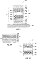
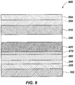
- FIG. 1 illustrates an embodiment of a magnetic cell structure 100 according to the present disclosure.
- the magnetic cell structure 100 includes a magnetic cell core 101 over a substrate 102.
- the magnetic cell core 101 may be disposed between an upper electrode 104 and a lower electrode 105.
- the magnetic cell core 101 includes a magnetic region and another magnetic region, for example, a "fixed region” 110 and a “free region” 120, respectively, with an oxide region (e.g., an "intermediate oxide region” 130) between.
- the sub-structure of the fixed region 110, free region 120, and intermediate oxide region 130 therebetween may be referred to herein as a magnetic tunnel junction ("MTJ") sub-structure 123 or MTJ structure 123.
- the intermediate oxide region 130 may be configured as a tunnel barrier region and may contact the fixed region 110 along interface 131 and may contact the free region 120 along interface 132.
- Either or both of the fixed region 110 and the free region 120 may be formed homogeneously or, optionally, may be formed to include more than one sub-region.
- a fixed region 110' of the magnetic cell core 101 may include multiple portions.
- the fixed region 110' may include a magnetic sub-region as an oxide-adjacent portion 113.
- An intermediate portion 115 such as a conductive sub-region, may separate the oxide-adjacent portion 113 from an electrode-adjacent portion 117.
- the electrode-adjacent portion 117 may include an alternating structure of magnetic sub-regions 118 and coupler sub-regions 119.
- one or more lower intermediary regions 140 may, optionally, be disposed under the magnetic regions (e.g., the fixed region 110 and the free region 120), and one or more upper intermediary regions 150 may, optionally, be disposed over the magnetic regions of the magnetic cell structure 100.
- the lower intermediary regions 140 and the upper intermediary regions 150 may be configured to inhibit diffusion of species between the lower electrode 105 and overlying materials and between the upper electrode 104 and underlying materials, respectively, during operation of the memory cell.
- the lower intermediary regions 140 and the upper intermediary regions 150 may, additionally or alternatively, include materials formulated to promote desired crystallization in neighboring materials.
- a secondary oxide region 170 is disposed proximate to the MTJ sub-structure 123.
- the secondary oxide region 170 may be adjacent the free region 120.
- the secondary oxide region 170 may directly physically contact the free region 120 along an interface 172.
- Such secondary oxide region 170 may, thus, be disposed to induce interfacial-MA in the magnetic material of the free region 120.
- the magnetic cell structure 100 may be configured with a "dual-oxide" structure.
- the free region 120 is also disposed proximate to a getter seed region 180.
- the getter seed region 180 may be spaced from the free region 120 by the secondary oxide region 170.
- the getter seed region 180 may directly physically contact the secondary oxide region 170 along an interface 178.
- the getter seed region 180 is formed from a precursor getter seed material comprising at least one getter species.
- the precursor getter seed material comprises at least two getter species, at least one of which being formulated to have a chemical affinity for a diffusive species from a neighboring precursor magnetic material and at least another of which being formulated to have a chemical affinity for a diffusive species, such as oxygen, from a neighboring precursor oxide material.
- the getter species having a chemical affinity for the diffusive species of the precursor magnetic material may also be included in the secondary oxide region 170.
- Each getter species may have a higher chemical affinity for its corresponding, targeted diffusive species than the chemical affinity between other species of the corresponding neighboring precursor material and the corresponding, targeted diffusive species.
- the initial presence of the diffusive species of the precursor magnetic material may inhibit crystallization of the precursor magnetic material, but the proximity of the getter seed region 180 to the precursor magnetic material may enable diffusion of the diffusive species from the precursor magnetic material to material of the getter seed region 180. Once diffused, the diffused species may chemically react with the getter species, forming a compound that remains in the getter seed region 180 in the final structure.
- the removal of the diffusive species from the precursor magnetic material leaves a depleted magnetic material (i.e., a magnetic material with a lower concentration of the diffusive species compared to a concentration before diffusion) that is able to crystallize into a desired crystal structure (e.g., a bcc (001)).
- the desired crystal structure may be propagated from one or more neighboring materials, e.g., the oxide of the intermediate oxide region 130.
- the crystallized, depleted magnetic material, having the desired crystal structure may exhibit high TMR (e.g., greater than about 100% (about 1.00), e.g., greater than about 120% (about 1.20).
- the diffusive species of the precursor oxide material may be oxygen (O), and its initial presence in the precursor oxide material contributes to electric resistances and high damping in the oxide material.
- the proximity of the getter seed region 180 to the precursor oxide material may enable diffusion of the oxygen (O) from the precursor oxide material to the getter seed region 180.
- the diffused oxygen (O) may chemically react with the other getter species, which may be referred to herein as the "oxygen-getter species," forming an oxide compound that remains in the getter seed region 180 in the final structure.
- the getter seed region 180 may be formulated to be amorphous and remain amorphous while the neighboring depleted magnetic material crystallizes.
- the precursor material of the getter seed region 180 may be amorphous when initially formed and may remain amorphous even at high temperatures, e.g., during an anneal, and even once enriched with the diffused species from the precursor magnetic material and the precursor oxide material.
- the material of the getter seed region 180 may not inhibit the crystallization of the neighboring depleted magnetic material.
- the thickness, composition, and structure of the getter seed region 180 may be selected to provide a sufficient amount of getter species-for the diffusive species from the precursor magnetic material-and a sufficient amount of oxygen-getter species-for the diffusive oxygen (O) from the precursor oxide material-in the getter seed region 180 to have a desired capacity to receive and bond with the diffused species from the neighboring precursor magnetic material and the neighboring precursor oxide material.
- a thicker getter seed region may have a relatively higher capacity for the diffused species, compared to a thinner getter seed region.
- the getter seed region 180 may be between about 7.5 ⁇ (about 0.75 nm) to about 30 ⁇ (about 3.0 nm) in thickness.
- the thickness, composition, and structure of the secondary oxide region 170 may be selected to enable diffusion of the diffusive species, from the precursor magnetic material, through the material of the secondary oxide region 170 to the getter seed region 180.
- the thickness of the secondary oxide region 170 may be tailored to be of a sufficiently high thickness so that interfacial-MA is induced along the interface 172 with the free region 120 while of a sufficiently low thickness so that the diffusive species from the precursor magnetic material may diffuse therethrough and so that enough oxygen can diffuse out of the material of the secondary oxide region 170 to the getter seed region 180, to provide low electrical resistance and low damping.
- the thickness of the secondary oxide region 170 may, therefore, be less than the thickness of the intermediate oxide region 130 in the MTJ sub-structure 123.
- the secondary oxide region 170 may be between about 2 ⁇ (about 0.2 nm) to about 10 ⁇ (about 1.0 nm) in thickness while the thickness of the intermediate oxide region 130 may be between about 5 ⁇ (about 0.5 nm) to about 10 ⁇ (about 1.0 nm).
- additional getter seed regions may be present.
- another getter seed region may be disposed internal to the secondary oxide region 170 or laterally adjacent to one or both of the secondary oxide region 170 and the free region 120.
- the additional getter seed regions may also be formulated to receive diffused species from the precursor magnetic material of the free region 120 and formulated to receive oxygen diffused from the precursor oxide material of the secondary oxide region 170.
- the getter seed region 180 may be physically isolated from the fixed region 110 by one or more other regions, e.g., by the free region 120, the intermediate oxide region 130, and the secondary oxide region 170. Therefore, getter species of the getter seed region 180 may not chemically react with species of the fixed region 110.
- the magnetic cell structure 100 of FIG. 1 is configured as a "top-pinned” memory cell, i.e., a memory cell in which the fixed region 110 is disposed over the free region 120.
- the memory cell may be configured as a "bottom-pinned” memory cell, i.e., a memory cell in which the fixed region 110 is disposed under the free region 120.
- the secondary oxide region 170 may overlay the free region 120
- the getter seed region 180 may overlay the secondary oxide region 170.
- the getter seed region 180 may nonetheless be formulated to receive a species diffused from the precursor magnetic material of the free region 120, to enable propagation of a desired crystal structure from the intermediate oxide region 130 to the depleted magnetic material, and to receive oxygen diffused from the precursor oxide material of the secondary oxide region 170, to enable low electrical resistance and low damping in the secondary oxide region.
- any embodiment illustrated or otherwise described herein as being “top-pinned” may be alternatively embodied in a "bottom-pinned” configuration, e.g., by a reversal of the order of the regions of the cell core structure (e.g., the cell core structure 101 of FIG. 1 ).
- the memory cells of embodiments of the present disclosure may be configured as out-of-plane STT-MRAM cells, as in FIG. 1 , or, alternatively, as in-plane STT-MRAM cells, as illustrated in FIG. 1B .
- "In-plane" STT-MRAM cells include magnetic regions exhibiting a magnetic orientation that is predominantly oriented in a horizontal direction
- "out-of-plane” STT-MRAM cells include magnetic regions exhibiting a magnetic orientation that is predominantly oriented in a vertical direction.
- the STT-MRAM cell may be configured to exhibit a vertical magnetic orientation in at least one of the magnetic regions (e.g., the fixed region 110 and the free region 120).
- the vertical magnetic orientation exhibited may be characterized by perpendicular magnetic anisotropy ("PMA") strength.
- PMA perpendicular magnetic anisotropy
- each of the fixed region 110 and the free region 120 may exhibit a vertical magnetic orientation.
- the magnetic orientation of the fixed region 110 may remain "substantially fixed,” i.e., directed in essentially the same direction throughout operation of the STT-MRAM cell, for example, in the direction indicated by arrows 112 of FIG. 1 .
- the magnetic orientation of the free region 120 may be switched, during operation of the cell, between a parallel configuration and an anti-parallel configuration, as indicated by double-pointed arrows 122 of FIG. 1 .
- an in-plane STT-MRAM cell may be configured to exhibit a horizontal magnetic orientation in at least one of the magnetic regions (e.g., a fixed region 110" and a free region 120") of a MTJ sub-structure 123', as indicated by arrow 112 B in the fixed region 110" and double-pointed arrow 122 B in the free region 120".
- a memory cell comprising a magnetic cell core.
- the magnetic cell core comprises a magnetic tunnel junction sub-structure comprising a fixed region, a free region, and an intermediate oxide region between the fixed region and the free region.
- a secondary oxide region is adjacent the magnetic tunnel junction sub-structure.
- a getter seed region is proximate the secondary oxide region and comprises an oxygen-getter species bonded to oxygen. At least one of the secondary oxide region and the getter region comprise another getter species bonded to a diffused species diffused.
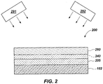
- an intermediate structure 200 may be formed with a conductive material 205 formed over the substrate 102, and a precursor getter seed material 280 over the conductive material 205.
- a precursor getter seed material 280 may be formed over the conductive material 205, before forming the precursor getter seed material 280 thereover.
- the conductive material 205, from which the lower electrode 105 ( FIG. 1 ) is formed may comprise, consist essentially of, or consist of, for example and without limitation, a metal (e.g., copper, tungsten, titanium, tantalum), a metal alloy, or a combination thereof.
- a metal e.g., copper, tungsten, titanium, tantalum
- a metal alloy e.g., copper, tungsten, titanium, tantalum
- the lower intermediary material 240 may comprise, consist essentially of, or consist of, for example and without limitation, tantalum (Ta), titanium (Ti), tantalum nitride (TaN), titanium nitride (TiN), ruthenium (Ru), tungsten (W), or a combination thereof.
- the lower intermediary material 240 if included, may be incorporated with the conductive material 205 from which the lower electrode 105 ( FIG. 1 ) is to be formed.
- the lower intermediary material 240 may be an upper-most sub-region of the conductive material 205.
- the precursor getter seed material 280 may be formed by, for example and without limitation, sputtering a material comprising at least one getter species over the previously-formed materials.
- the precursor getter seed material 280 is formulated to include at least one getter species selected to have a chemical affinity for a diffusive species from a precursor magnetic material, from which the free region 120 ( FIG. 1 ) is to be formed.
- the at least one getter species may be selected to having a higher chemical affinity for the diffusive species of the precursor magnetic material compared to a chemical affinity between the diffusive species and another species of the precursor magnetic material. Therefore, at least one getter species of the precursor getter seed material 280 is formulated to attract the diffusive species from the precursor magnetic material.
- the precursor getter seed material 280 is also formulated to include at least another getter species selected to have a chemical affinity for a diffusive species from a precursor oxide material, from which the secondary oxide region 170 ( FIG. 1 ) is to be formed.
- the at least another getter species may be selected to have a higher chemical affinity for oxygen (O) of the precursor oxide material compared to a chemical affinity between oxygen and another species of the precursor oxide material. Therefore, at least another getter species of the precursor getter seed material 280 is formulated to attract a diffusive species, e.g., oxygen (O), from the precursor oxide material.
- each species of the precursor getter seed material 280 may be formulated to have a chemical affinity for (i.e., be compatible to chemically bond with) at least one of the diffused species from the precursor magnetic material and the diffused species (e.g., oxygen (O)) from the precursor oxide material.
- the precursor getter seed material 280 may include species non-reactive with one or both of the diffused species or may consist of or consist essentially of species that react with one or both of the diffused species.
- the precursor getter seed material 280 may be formed by sputtering (i.e., physical vapor deposition (PVD) using one or more targets 291, 292.
- PVD physical vapor deposition
- two sputter targets 291, 292 may be used simultaneously, with a sputter target 291 formulated to comprise the getter species with a chemical affinity for the diffusive species of the precursor magnetic material and with another sputter target 292 formulated to comprise the getter species (e.g., an oxygen-getter species) with a chemical affinity for the diffusive species (e.g., oxygen (O)) of the precursor oxide material.
- Both targets 291, 292 may be used simultaneously such that the species intermix and substantially evenly distribute as the precursor getter seed material 280 is formed.
- a precursor oxide material 370 from which the secondary oxide region 170 ( FIG. 1 ) is to be formed, may comprise, consist essentially of, or consist of, for example and without limitation, a nonmagnetic oxide material (e.g., magnesium oxide (MgO), aluminum oxide (Al 2 O 3 ), titanium oxide (TiO 2 ), or other oxide materials of conventional tunnel barrier regions of MTJ sub-structures).
- a nonmagnetic oxide material e.g., magnesium oxide (MgO), aluminum oxide (Al 2 O 3 ), titanium oxide (TiO 2 ), or other oxide materials of conventional tunnel barrier regions of MTJ sub-structures.
- the precursor oxide material 370 may be formed (e.g., grown, deposited) directly on the precursor getter seed material 280.
- At least one precursor magnetic material 320 may be formed over the precursor getter seed material 280, as also illustrated in FIG. 3 .
- Co cobalt
- Fe iron
- B boron
- the precursor magnetic material 320 may comprise at least one of Co, Fe, and B (e.g., a CoFeB material, a FeB material, a CoB material).
- the precursor magnetic material 320 may alternatively or additionally include nickel (Ni) (e.g., an NiB material).
- the precursor magnetic material 320 may be formed as a homogeneous region.
- the precursor magnetic material 320 may include one or more sub-regions, e.g., of CoFeB material, with the sub-regions having different relative atomic ratios of Co, Fe, and B.
- the precursor magnetic material 320 includes at least one diffusive species 321.
- the diffusive species 321 is such that its absence, in whole or in part, would not inhibit the precursor magnetic material 320, or a depleted magnetic material formed therefrom, from exhibiting magnetism.
- the presence of the diffusive species 321 in the precursor magnetic material 320 may enable the precursor magnetic material 320 to be formed (e.g., by sputtering) in an amorphous state.
- the precursor oxide material 370 includes at least one diffusive species 372.
- the diffusive species 372 is such that its absence, from the body of the precursor oxide material 370, will not inhibit the precursor oxide material 370, or a depleted oxide material formed therefrom, from inducing interfacial-MA with the precursor magnetic material 320 or the depleted magnetic material. Rather, the presence of the diffusive species 372 along only the interface 172 between the precursor oxide material 370 (or resulting depleted oxide material) and the precursor magnetic material 320 (or resulting depleted magnetic material) may enable the inducement of interfacial-MA.
- the precursor getter seed material 280 may be formulated to include at least two getter species, including a getter species 281 and another getter species 282.
- the getter species 281 is formulated to have a chemical affinity for the diffusive species 321 of the precursor magnetic material 320
- the another getter species 282 is formulated to have a chemical affinity for the diffusive species 372 of the precursor oxide material 370.
- the getter species 281 of the precursor getter seed material 280 may be selected to have an endothermic heat of formation of a compound between the getter species 281 and the diffusive species 321 from the precursor magnetic material 320. Moreover, the getter species 281 may be selected to be electrically conductive (e.g., may comprise a conductive metal), so as to increase the conductivity of the getter seed region 180 ( FIG. 1 ) of the final structure. Finally, the getter species 281 may be selected to be substantially non-reactive with the another getter species 282 and to enable the precursor getter seed material 280 to exhibit an amorphous structure at up to high temperatures (e.g., at least about 500 °C).
- high temperatures e.g., at least about 500 °C
- the precursor getter seed material 280 may include, as the getter species 281 having a chemical affinity for the diffusive species 321 of the precursor magnetic material 320, at least one of tantalum (Ta), ruthenium (Ru), tungsten (W), aluminum (Al), titanium (Ti), zirconium (Zr), nitrogen (N), hafnium (Hf), and nickel (Ni).
- the precursor magnetic material 320 may be a CoFeB magnetic material, the boron (B) thereof being the diffusive species 321.
- the precursor getter seed material 280 (and, for example, the target 291 ( FIG. 2 )) may be formulated to comprise, consist essentially of, or consist of tungsten-ruthenium-nitrogen (W-Ru-N) with an atomic ratio of about 49.5:49.5:1.0. Such a composition is formulated to exhibit an amorphous structure up to high temperatures (e.g., up to about 500° C.).
- Each of the tungsten (W), ruthenium (Ru), and nitrogen (N) may be the getter species 281 exhibiting a chemical affinity for the boron (B) diffusive species 321.
- the precursor getter seed material 280 (and, for example, the target 291 ( FIG. 2 )) may be formulated to comprise, consist essentially of, or consist of: tungsten-nitrogen (W-N) with an atomic ratio of about 75:25, wherein both the tungsten (W) and the nitrogen (N) may be the getter species 281 exhibiting a chemical affinity for the boron (B) diffusive species 321; tungsten-ruthenium-boron (W-Ru-B) with an atomic ratio of about 46:37:17, wherein the tungsten (W) and the ruthenium (Ru) may be the getter species 281 exhibiting a chemical affinity for the boron (B); tungsten-ruthenium (W-Ru) with an atomic ratio of about 45:55, w herein the tungsten (W) and the ruthenium (Ru) may be the getter species 281 exhibiting a chemical affinity for the boron (B); and iron-cobalt-
- the presence of nitrogen (N) in the material also enables low damping, and thus lower programming currents, in the resulting cell structure.
- the another getter species 282 of the precursor getter seed material 280 may be selected to have a heat of formation, of a compound between the another getter species 282 and the another diffusive species 372 from the precursor oxide material 270, that is less than or about equal to the heat of formation of a compound between the another diffusive species 372 and another species of the precursor oxide material 270.
- the secondary oxide material 370 is formulated to consist essentially of magnesium oxide (MgO)
- the another getter species 282 may be selected to have a lower heat of formation with oxygen (O), being the another diffusive species 372, compared to a heat of formation between oxygen (O) and the magnesium (Mg) of the MgO.
- the precursor getter seed material 280 may include, as the another getter species 282, at least one of calcium (Ca), strontium (Sr), beryllium (Be), lanthanum (La), barium (Ba), aluminum (Al), and magnesium (Mg).
- the another getter species 282 at least one of calcium (Ca), strontium (Sr), beryllium (Be), lanthanum (La), barium (Ba), aluminum (Al), and magnesium (Mg).
- An oxide material 330 from which the intermediate oxide region 130 ( FIG. 1 ) is formed, may be formed on the precursor magnetic material 320, e.g., before an anneal during which the precursor magnetic material 320 (or, rather, a depleted magnetic material formed from the precursor magnetic material 320) is crystallized through propagation of a crystal structure from the oxide material 330.
- the oxide material 330 may comprise, consist essentially of, or consist of, for example and without limitation, a nonmagnetic oxide material (e.g., magnesium oxide (MgO), aluminum oxide (Al 2 O 3 ), titanium oxide (TiO 2 ), or other oxide materials of conventional MTJ nonmagnetic regions).
- a nonmagnetic oxide material e.g., magnesium oxide (MgO), aluminum oxide (Al 2 O 3 ), titanium oxide (TiO 2 ), or other oxide materials of conventional MTJ nonmagnetic regions.
- the another oxide material 330 may be the same material as the precursor oxide material 370 or a material comprising the same elements as the precursor oxide material 370 though with different atomic ratios thereof.
- both of the oxide material 330 and precursor another oxide material 370 may comprise, consist essentially of, or consist of MgO.
- the oxide material 330 may be formed (e.g., grown, deposited) directly on the precursor magnetic material 320.
- the oxide material 330 may be crystalline (e.g., with the bcc (001) structure) when initially formed or may later be crystallized during anneal.
- the oxide material 330 may be positioned such that, during anneal of, e.g., an intermediate structure 300 of FIG. 3 , the desired crystal structure may propagate to a neighboring magnetic material (e.g., a depleted magnetic material 420 ( FIG. 4 )) to enable the magnetic material (e.g., the depleted magnetic material 420 ( FIG. 4 )) to crystallize into the same crystal structure (e.g., the bcc (001) structure).
- a neighboring magnetic material e.g., a depleted magnetic material 420 ( FIG. 4 )
- the magnetic material e.g., the depleted magnetic material 420 ( FIG. 4 )
- the diffusive species 321 may transfer (e.g., diffuse) from the precursor magnetic material 320, through the precursor oxide material 370, to the precursor getter seed material 280.
- the another diffusive species 372 may transfer (e.g., diffuse) from the precursor oxide material 370 to the precursor getter seed material 280. As this occurs, as illustrated in FIGS.
- the getter species 281 may react with and bond to the diffusive species 321 (now referred to, herein, as a diffused species 321'), and the another getter species 282 may react with and bond to the another diffusive species 372 (now referred to, herein, as another diffused species 372').
- the precursor magnetic material 320 FIG. 3
- the precursor oxide material 370 FIG. 3
- the precursor getter seed material 280 FIG. 3
- the depleted oxide region 470 may not be completely devoid of the another diffusive species 372. Rather, an amount of the oxygen (O) may remain proximate the interface 172 with the depleted magnetic material 420. Thus, any oxygen remaining in the depleted oxide material 470 may include a maximum oxygen concentration along the interface 172. Therefore, oxygen (O) at the interface 172 may function to bond with, e.g., iron (Fe) in the depleted magnetic material 420 to induce interfacial-MA along the interface 172.
- oxygen (O) at the interface 172 may function to bond with, e.g., iron (Fe) in the depleted magnetic material 420 to induce interfacial-MA along the interface 172.
- the decreased concentration of oxygen (O) throughout the remainder of the depleted oxide material 470 may reduce the electrical resistance of the depleted oxide material 470.
- the reduction, but not complete depletion, of oxygen may enable the depleted oxide material 470 to be electrically conductive.
- the resulting magnetic cell structure may include dual oxide regions (i.e., the intermediate oxide region 130 and the secondary oxide region 170 ( FIG. 1 ), formed from the depleted oxide material 470) without degrading the electrical resistance (i.e., without substantially raising the electrical resistance) of the memory cell.
- the enriched getter seed material 480 includes the diffused species 321', the another diffused species 372', the getter species 281, and the another getter species 282. Therefore, in an embodiment in which the precursor magnetic material 320 ( FIG. 3 ) was formulated as a CoFeB material and the precursor oxide material 370 ( FIG.
- the enriched getter seed material 480 may include the boron (B) (as the diffused species 321') from the CoFeB material, and a portion of the oxygen (O) (as the another diffused species 372') from the MgO, leaving some of oxygen (O) (as the diffusive species 372) along the interface 172 with the CoFe depleted magnetic material 420.
- a memory cell comprising a magnetic region comprising cobalt (Co) and iron (Fe).
- the magnetic region exhibits a switchable magnetic orientation.
- An oxide region is disposed between the magnetic region and another magnetic region exhibiting a substantially fixed magnetic orientation.
- Another oxide region is adjacent the magnetic region and comprises oxygen concentrated proximate an interface with the magnetic region.
- An amorphous getter seed region is adjacent the another oxide region.
- the getter seed region comprises oxygen, boron, an oxygen-getter species, and a boron-getter species.
- the precursor getter seed material 280 may be formulated to be amorphous when initially formed over the substrate 102 and to remain amorphous when converted to the enriched getter seed material 480.
- the atomic ratios of the getter species 281, 282 in the precursor getter seed material 280 may be selected to tailor the atomic ratios in the final, enriched getter seed material 480 to a composition that will be amorphous and remain amorphous at high anneal temperatures.
- the precursor getter seed material 280 ( FIG. 3 ) may be formulated such that the precursor getter seed material 280 is stable (e.g., species will not out-diffuse) at high temperatures used during anneal for crystallizing the depleted magnetic material 420. Therefore, the high temperatures that promote crystallization of the depleted magnetic material 420 (e.g., by crystal structure propagation from the oxide material 330) to a desired crystal structure (e.g., a bcc (001) structure) may be utilized without the precursor getter seed material 280 inhibiting the crystallization.
- a desired crystal structure e.g., a bcc (001) structure
- the amorphous nature of the enriched getter seed material 480 avoids microstructure defects in the depleted magnetic material 420 that may otherwise form if the enriched getter seed material 480 had a microstructure that differed from and competed with that of the desired crystal structure (e.g., the bcc (001) structure) as the crystal structure propagated to the depleted magnetic material 420 from a neighboring material (e.g., oxide material 330 ( FIG. 3 ) for the intermediate oxide region 130 ( FIG. 1 )).
- the desired crystal structure e.g., the bcc (001) structure
- the depleted magnetic material 420 may be formed to exhibit the desired crystal structure, due to lack of interference, by the depleted oxide material 470, with the crystal structure propagation between the oxide material 330 of the intermediate oxide region 130 ( FIG. 1 ) to the depleted magnetic material 420, the free region 120 ( FIG. 1 ) may be formed to exhibit a crystal structure that promotes high TMR.
- the precursor magnetic material 320 ( FIG. 3 ) was formulated to be a CoFeB material
- removing the diffusive species 321 ( FIG. 3A ) of boron (B) from the CoFeB precursor magnetic material 320 with a precursor getter seed material 280 having the getter species 281 having a chemical affinity for the boron (B) may enable crystallization of the depleted magnetic material 420 at a lower temperature than the crystallization temperature of the CoFeB (i.e., the precursor magnetic material 320 ( FIG. 3 ) still including the diffusive species 321).
- an anneal temperature used may enable crystallization of the depleted magnetic material 420 (e.g., by propagating the desired crystal structure from a neighboring material, e.g., the oxide material 330 of the intermediate oxide region 130 ( FIG. 1 )) without being so high as to degrade neighboring materials (e.g., without out-diffusing a species, e.g., tungsten (W), from the enriched getter seed material 480).
- a neighboring material e.g., the oxide material 330 of the intermediate oxide region 130 ( FIG. 1 .
- the depleted magnetic material 420 may, therefore, be crystallized into a desired crystal structure (e.g., a bcc (001) crystal structure) that enables formation of a magnetic cell structure (e.g., the magnetic cell structure 100 ( FIG. 1 )) without suffering from substantial structural defects.
- a desired crystal structure e.g., a bcc (001) crystal structure
- the absence of substantial structural defects may enable a high TMR.
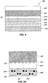
- Other materials of the intermediate structure 300 may also be crystallized due to annealing to form an annealed structure 400 ( FIG. 4 ).
- the annealing process may be conducted at an annealing temperature of from about 300° C to about 700° C (e.g., about 500° C) and may be held at the annealing temperature for from about one minute (about 1 min.) to about one hour (about 1 hr.).
- the annealing temperature and time may be tailored based on the materials of the intermediate structure 300, the desired crystal structure of, e.g., the depleted magnetic material 420, a desired amount of depletion of the diffused species 321' from the precursor magnetic material 320 ( FIG. 3 ), and a desired amount of depletion of the another diffused species 372' from the precursor oxide material 370 ( FIG. 3 ).
- removal of the diffusive species 321 ( FIG. 3A ) from the precursor magnetic material 320 ( FIG. 3 ) may promote crystallization of the depleted magnetic material 420, it is further contemplated, without being limited to any particular theory, that removal may also promote inducement of MA along the interface 172 between the depleted magnetic material 420 and the depleted oxide material 470, along the interface 132 ( FIG. 1 ) between the depleted magnetic material 420 and the intermediate oxide region 130 ( FIG. 1 ), or along both interfaces 172, 132.
- the diffusive species 321 FIG. 3A
- the other species of the depleted magnetic material 420 may have more interaction with the oxide material than the other species would have if the diffusive species 321 were still incorporated in the precursor magnetic material 320.
- the retention of the diffused species 321' ( FIG. 4A ), via chemical bonds with the getter species 281, in the enriched getter seed material 480 may avoid the diffused species 321' diffusing to the interfaces 172, 132 ( FIG. 1 ) between the magnetic region (e.g., the free region 120) and its neighboring MA-inducing oxide regions. This may enable more MA-inducing interaction along the interfaces 172, 132 ( FIG. 1 ) than may otherwise be achieved.
- the MA strength may be greater, due to the presence of the precursor getter seed material 280 (or, rather, the enriched getter seed material 480) than the MA strength of the same structure without the precursor getter seed material 280 (or, rather, the enriched getter seed material 480).
- the diffusion of boron (B) diffusive species 321 from the precursor magnetic material 320 may inhibit the boron (B) diffusive species 321 from lingering along the interface 172, where it may otherwise interfere with the inducement of interfacial MA. It is contemplated that, with a substantial amount of boron (B) along the interface 172, the presence of the boron (B) may inhibit formation of bonds between the magnetic material (e.g., the depleted magnetic material 420 ( FIG.4 )) and the oxide material (e.g., the depleted oxide material 470 ( FIG.
- the proximity of the getter species 281, in the precursor getter seed material 380, to the precursor magnetic material 320, may enable higher interfacial-MA inducement because the diffusive species 321 may be directed to the precursor getter seed material 380 and away from the interface 172.
- the free region 120 ( FIG. 1 ) is described as being “formed from” the precursor magnetic material 320 (e.g., a CoFeB material) that comprises the diffusive species 321 ( FIG. 3A )
- the free region 120 of the fabricated, magnetic cell core 101 (or any cell core of the present disclosure) may comprise substantially less of the diffusive species 321 (e.g., the boron (B)) than when the precursor magnetic material 320 was initially formed.
- the secondary oxide region 170 ( FIG. 1 ) is described as being “formed from” the precursor oxide material 320 ( FIG.
- the secondary oxide region 170 of the fabricated, magnetic cell core 101 may comprise substantially less of the another diffusive species 372 (e.g., the oxygen (O)) than when the precursor oxide material 370 was initially formed.
- the another diffusive species 372 e.g., oxygen (O)
- the secondary oxide region 170 of the fabricated, magnetic cell core 101 FIG. 1
- any cell core of the present disclosure may comprise substantially less of the another diffusive species 372 (e.g., the oxygen (O)) than when the precursor oxide material 370 was initially formed.
- the other materials of the magnetic cell structure may be formed over the annealed intermediate structure 400, to form a precursor structure 500 as illustrated in FIG. 5 .
- the other materials of the magnetic cell structure 100 may be formed over, e.g., the oxide material 330, e.g., before the anneal, and may be annealed along with the lower materials.
- another magnetic material 510 from which the fixed region 110 ( FIG. 1 ) is to be formed, may be formed (e.g., grown, deposited) directly on the oxide material 330, e.g., before or after the anneal stage that crystallizes the depleted magnetic material 420.
- the another magnetic material 510 may comprise a CoFeB material.
- the another magnetic material 510 may include the same material as the precursor magnetic material 320 ( FIG. 3 ), or a material having the same elements, though in different atomic ratios.
- an intermediate material for the intermediate portion 115 ( FIG. 1A ), may be formed over the another magnetic material 510.
- the intermediate material may comprise, consist essentially of, or consist of a conductive material (e.g., tantalum (Ta)). Alternating magnetic material and coupler material, for the magnetic sub-regions 118 ( FIG. 1A ) and coupler sub-regions 119 ( FIG. 1A ), respectively, may be formed on the intermediate material.
- the alternating magnetic and coupler materials may comprise, consist essentially of, or consist of cobalt/palladium (Co/Pd) multi-sub-regions; cobalt/platinum (Co/Pt) multi-sub-regions; cobalt/nickel (Co/Ni) multi-sub-regions; cobalt/iridium (Co/Ir) multi-sub-regions; cobalt/iron/terbium (Co/Fe/Tb) based materials, L 1 0 materials, coupler materials, or other magnetic materials of conventional fixed regions.
- one or more upper intermediary materials 550 may be formed over the another magnetic material 510 (and any other materials from which the fixed region 110 ( FIG. 1 ) is to be formed).
- the upper intermediary materials 550 which, if included, form the optional upper intermediary regions 150 ( FIG. 1 ), may comprise, consist essentially of, or consist of materials configured to ensure a desired crystal structure in neighboring materials.
- the upper intermediary materials 550 may alternatively or additionally include metal materials configured to aid in patterning processes during fabrication of the magnetic cell, barrier materials, or other materials of conventional STT-MRAM cell core structures.
- the upper intermediary material 550 may include a conductive material (e.g., one or more materials such as copper, tantalum, titanium, tungsten, ruthenium, hafnium, zirconium, tantalum nitride, or titanium nitride) to be formed into a conductive capping region.
- a conductive material e.g., one or more materials such as copper, tantalum, titanium, tungsten, ruthenium, hafnium, zirconium, tantalum nitride, or titanium nitride
- Another conductive material 504, from which the upper electrode 104 ( FIG. 1 ) may be formed, may be formed over the another magnetic material 510 (and any other materials from which the fixed region 110 ( FIG. 1 ) is to be formed) and, if present, the upper intermediary materials 550.
- the another conductive material 504 and the upper intermediary materials 550, if present, may be integrated with one another, e.g., with the upper intermediary materials 550 being lower sub-regions of the conductive material 504.
- the precursor structure 500 may then be patterned, in one or more stages, to form the magnetic cell structure 100, according to the embodiment illustrated in FIG. 1 .
- Techniques for patterning structures such as the precursor structure 500 to form structures such as the magnetic cell structure 100 ( FIG. 1 ) are known in the art and so are not described herein in detail.
- the magnetic cell structure 100 includes the magnetic cell core 101 including the secondary oxide region 170 and the getter seed region 180 proximate to the free region 120.
- the free region 120 includes the depleted magnetic material 420 ( FIG. 4 ), formed from the precursor magnetic material 320 ( FIG. 3 ) and comprises a lower concentration of the diffusive species 321 ( FIG. 3A ) than a free region formed from the precursor magnetic material 320 ( FIG. 3 ) without the getter seed region 180 proximate thereto.
- the secondary oxide region 170 includes the depleted oxide material 470 ( FIG. 4 ), formed from the precursor oxide material 370 ( FIG. 3 ) and comprises a lower concentration of the another diffusive species 372 ( FIG. 3A ) than a secondary oxide region formed from the precursor oxide material 370 ( FIG. 3 ) without the getter seed region 180 proximate thereto.
- the magnetic region proximate to the getter seed region 180 may be substantially or completely depleted of the diffusive species 321. In other embodiments, the magnetic region may be partially depleted of the diffusive species 321. In such embodiments, the magnetic region or regions may have a gradient of the diffusive species 321 (in embodiments of the invention, boron) therethrough, with a low concentration of the diffusive species 321 adjacent to the getter seed region 180, along interface 172 ( FIG. 1 ), and a high concentration of the diffusive species 321 opposite the getter seed region 180, along interface 132 ( FIG. 1 ), relative to one another. The concentration of the diffusive species 321 may, in some embodiments, equilibrate after or during anneal.
- the free region 120 formed with a crystalline, depleted magnetic material 420 ( FIG. 4 ), may have a desired crystal structure that may be substantially free of defects, due, at least in part, to the removal of the diffusive species 321 and the bonding of the diffused species 321 to the getter species 281 and due, at least in part, to the amorphous microstructure of the getter seed region 180.
- the crystallinity of the free region 120 may enable the magnetic cell structure 100 to exhibit a high TMR during use and operation. Furthermore, the depleted magnetic material 420 of the free region 120 may promote MA-inducement with neighboring oxide regions (e.g., the secondary oxide region 170 and the intermediate oxide region 130).
- the secondary oxide region 170 formed with the depleted oxide material 470 ( FIG. 4 ), may have low electrical resistance, e.g., may be electrically conductive, with a maximum oxygen concentration along the interface 172 with the free region 120.
- high MA strength may be promoted due to MA-inducement in the free region 120 from both of the dual oxide regions (i.e., the intermediate oxide region 130 and the secondary oxide region 170) without also exhibiting high electrical resistance (e.g., high resistance area (RA)) and high damping.
- the getter seed region 180 includes nitrogen (N)
- low damping may be even further enabled.
- Forming a precursor structure comprises forming a precursor getter seed material over a substrate.
- a precursor oxide material is formed over the precursor getter seed material.
- a precursor magnetic material is formed over the precursor oxide material.
- a diffusive species comprising boron is diffused from the precursor magnetic material, and oxygen is diffused from the precursor oxide material, to the precursor getter seed material to convert at least a portion of the precursor magnetic material into a depleted magnetic material, to convert at least a portion of the precursor oxide material into an oxygen-depleted material, and to convert at least a portion of the precursor getter seed material into an enriched getter seed material.
- the precursor structure is patterned to form a cell core structure comprising a getter seed region formed from the enriched getter seed material, a secondary oxide region formed from the oxygen-depleted material, and a free region formed from the depleted magnetic material.
- the magnetic cell structure 600 includes a magnetic cell core 601 comprising a getter secondary oxide region 670.
- the getter secondary oxide region 670 may be formed from a precursor getter oxide material 770, as illustrated in FIG. 7 , that includes the same material as the precursor oxide material 370 ( FIG. 3 ) described above, while also including additional getter species 281', formulated to have a chemical affinity for the diffusive species (boron) 321 of the precursor magnetic material 320.
- the precursor getter oxide material 770 may include magnesium oxide (MgO) with the additional getter species 281' added.
- the precursor getter oxide material 770 may be disposed, within an intermediate structure 700, between the precursor getter seed material 280 and the precursor magnetic material 320.
- an annealed structure 800 includes an "enriched-depleted" oxide material 870, formed from the precursor getter oxide material 770.
- the enriched-depleted oxide material 870 is both enriched with some amount of the diffused species 321', bonded to the additional getter species 281', and depleted of the another diffusive species 372 (e.g., oxygen (O)), except along the interface 172.
- the additional getter species 281' may be the same as, or different than, the getter species 281 in the enriched getter seed material 480. Thus, the additional getter species 281' may be selected from any of the species described above with respect to the getter species 281.
- the additional getter species 281' may be implanted into the precursor oxide material 370 ( FIG. 3 ), before formation of the precursor magnetic material 320.
- the additional getter species 281' may be incorporated into the precursor oxide material 370 ( FIG. 3 ) by co-sputtering of both the additional getter species 281' and the precursor oxide material 370 using physical vapor deposition (PVD).
- PVD physical vapor deposition
- the additional getter species 281' may be introduced in the form of a gas during deposition of the precursor oxide material 370.
- the remaining materials of a precursor structure 900 may then be formed, as illustrated in FIG. 9 , and the precursor structure 900 patterned to form the magnetic cell structure 600 of FIG. 6 .
- the secondary oxide region 170 ( FIG. 1 ) or the getter secondary oxide region 670 ( FIG. 6 ) is formulated to comprise magnesium oxide (MgO)
- an atomic ratio of the magnesium (Mg) to the oxygen (O) to the getter species 281 (e.g., boron-getter species), including the additional getter species 281' (if using the precursor getter oxide material 770), to the another getter species 282 (e.g., oxygen-getter species) (i.e., the Mg:O:B-getter:O-getter atomic ratio) may be from about 40:40:10:10 to about 45:45:5:5. Therefore, one or more of the getter species 281, including the additional getter species 281' (if included) and the another getter species 282 may be at low atomic levels (e.g., "dopant" levels of less than about 10 at. %, e.g., less than about 5 at. %, e.g., less than about 2 at. %).
- the method comprises forming an amorphous precursor getter seed material over a substrate.
- the amorphous precursor getter seed material comprises a boron-getter species and an oxygen-getter species.
- a precursor oxide material, comprising oxygen is formed over the amorphous precursor getter seed material.
- a precursor magnetic material, comprising boron is formed over the precursor oxide material. Another oxide material is formed over the precursor magnetic material.
- At least the precursor magnetic material and the precursor oxide material are annealed to react the boron from the precursor magnetic material with the boron-getter species of the amorphous precursor getter seed material and to react the oxygen from the precursor oxide material with the oxygen-getter species of the amorphous precursor getter seed material.
- an STT-MRAM system 1000 that includes peripheral devices 1012 in operable communication with an STT-MRAM cell 1014, a grouping of which may be fabricated to form an array of memory cells in a grid pattern including a number of rows and columns, or in various other arrangements, depending on the system requirements and fabrication technology.
- the STT-MRAM cell 1014 includes a magnetic cell core 1002, an access transistor 1003, a conductive material that may function as a data/sense line 1004 (e.g., a bit line), a conductive material that may function as an access line 1005 (e.g., a word line), and a conductive material that may function as a source line 1006.
- the peripheral devices 1012 of the STT-MRAM system 1000 may include read/write circuitry 1007, a bit line reference 1008, and a sense amplifier 1009.
- the cell core 1002 may be any one of the magnetic cell cores (e.g., the magnetic cell cores 101 ( FIG. 1 ), 601 ( FIG. 6 )) described above. Due to the structure of the cell core 1002, the method of fabrication, or both, the STT-MRAM cell 1014 may have high MA strength, low resistance (e.g., low resistance-area (RA) product), low damping, and high TMR.
- RA resistance-area
- an STT-MRAM cell 1014 In use and operation, when an STT-MRAM cell 1014 is selected to be programmed, a programming current is applied to the STT-MRAM cell 1014, and the current is spin-polarized by the fixed region of the cell core 1002 and exerts a torque on the free region of the cell core 1002, which switches the magnetization of the free region to "write to" or "program” the STT-MRAM cell 1014. In a read operation of the STT-MRAM cell 1014, a current is used to detect the resistance state of the cell core 1002.
- the read/write circuitry 1007 may generate a write current (i.e., a programming current) to the data/sense line 1004 and the source line 1006.
- a write current i.e., a programming current
- the polarity of the voltage between the data/sense line 1004 and the source line 1006 determines the switch in magnetic orientation of the free region in the cell core 1002.
- the free region is magnetized according to the spin polarity of the programming current, the programmed logic state is written to the STT-MRAM cell 1014.
- the read/write circuitry 1007 To read the STT-MRAM cell 1014, the read/write circuitry 1007 generates a read voltage to the data/sense line 1004 and the source line 1006 through the cell core 1002 and the access transistor 1003.
- the programmed state of the STT-MRAM cell 1014 relates to the electrical resistance across the cell core 1002, which may be determined by the voltage difference between the data/sense line 1004 and the source line 1006. In some embodiments, the voltage difference may be compared to the bit line reference 1008 and amplified by the sense amplifier 1009.
- FIG. 10 illustrates one example of an operable STT-MRAM system 1000. It is contemplated, however, that the magnetic cell cores 101 ( FIG. 1 ), 601 ( FIG. 6 ) may be incorporated and utilized within any STT-MRAM system configured to incorporate a magnetic cell core having magnetic regions.
- a semiconductor device comprising a spin torque transfer magnetic random access memory (STT-MRAM) array comprising STT-MRAM cells.
- At least one STT-MRAM cell of the STT-MRAM cells comprises a magnetic tunnel junction sub-structure over a substrate.
- the magnetic tunnel junction sub-structure comprises a free region, a fixed region, and an intermediate oxide region.
- the free region exhibits a vertical, switchable magnetic orientation.
- the fixed region exhibits a vertical, substantially fixed magnetic orientation.
- the intermediate oxide region is between the free region and the fixed region. Another oxide region contacts the free region.
- An amorphous region is proximate the free region and the another oxide region.
- the amorphous region comprises boron and oxygen.
- the semiconductor device 1100 includes a memory array 1102 and a control logic component 1104.
- the memory array 1102 may include a plurality of the STT-MRAM cells 1014 ( FIG. 10 ) including any of the magnetic cell cores (e.g., the magnetic cell cores 101 ( FIG. 1 ), 601 ( FIG. 6 )) discussed above, which magnetic cell cores (e.g., the magnetic cell cores 101 ( FIG. 1 ), 601 ( FIG. 6 )) may have been formed according to a method described above and may be operated according to a method described above.
- the control logic component 1104 may be configured to operatively interact with the memory array 1102 so as to read from or write to any or all memory cells (e.g., STT-MRAM cell 1014 ( FIG. 10 )) within the memory array 1102.
- the processor-based system 1200 may include various electronic devices manufactured in accordance with embodiments of the present disclosure.
- the processor-based system 1200 may be any of a variety of types such as a computer, pager, cellular phone, personal organizer, control circuit, or other electronic device.
- the processor-based system 1200 may include one or more processors 1202, such as a microprocessor, to control the processing of system functions and requests in the processor-based system 1200.
- the processor 1202 and other subcomponents of the processor-based system 1200 may include magnetic memory devices manufactured in accordance with embodiments of the present disclosure.
- the processor-based system 1200 may include a power supply 1204 in operable communication with the processor 1202.
- the power supply 1204 may include one or more of a fuel cell, a power scavenging device, permanent batteries, replaceable batteries, and rechargeable batteries.
- the power supply 1204 may also include an AC adapter; therefore, the processor-based system 1200 may be plugged into a wall outlet, for example.
- the power supply 1204 may also include a DC adapter such that the processor-based system 1200 may be plugged into a vehicle cigarette lighter or a vehicle power port, for example.
- a user interface 1206 may be coupled to the processor 1202.
- the user interface 1206 may include input devices such as buttons, switches, a keyboard, a light pen, a mouse, a digitizer and stylus, a touch screen, a voice recognition system, a microphone, or a combination thereof.
- a display 1208 may also be coupled to the processor 1202.
- the display 1208 may include an LCD display, an SED display, a CRT display, a DLP display, a plasma display, an OLED display, an LED display, a three-dimensional projection, an audio display, or a combination thereof.
- an RF sub-system/baseband processor 1210 may also be coupled to the processor 1202.
- the RF sub-system/baseband processor 1210 may include an antenna that is coupled to an RF receiver and to an RF transmitter (not shown).
- a communication port 1212, or more than one communication port 1212, may also be coupled to the processor 1202.
- the communication port 1212 may be adapted to be coupled to one or more peripheral devices 1214, such as a modem, a printer, a computer, a scanner, or a camera, or to a network, such as a local area network, remote area network, intranet, or the Internet, for example.
- the processor 1202 may control the processor-based system 1200 by implementing software programs stored in the memory.
- the software programs may include an operating system, database software, drafting software, word processing software, media editing software, or media playing software, for example.
- the memory is operably coupled to the processor 1202 to store and facilitate execution of various programs.
- the processor 1202 may be coupled to system memory 1216, which may include one or more of spin torque transfer magnetic random access memory (STT-MRAM), magnetic random access memory (MRAM), dynamic random access memory (DRAM), static random access memory (SRAM), racetrack memory, and other known memory types.
- the system memory 1216 may include volatile memory, non-volatile memory, or a combination thereof.
- the system memory 1216 is typically large so that it can store dynamically loaded applications and data.
- the system memory 1216 may include semiconductor devices, such as the semiconductor device 1100 of FIG. 11 , memory cells including any of the magnetic cell cores 101 ( FIG. 1 ), 601 ( FIG. 6 ) described above, or a combination thereof
- the processor 1202 may also be coupled to non-volatile memory 1218, which is not to suggest that system memory 1216 is necessarily volatile.
- the non-volatile memory 1218 may include one or more of STT-MRAM, MRAM, read-only memory (ROM) such as an EPROM, resistive read-only memory (RROM), and flash memory to be used in conjunction with the system memory 1216.
- ROM read-only memory
- RROM resistive read-only memory
- flash memory to be used in conjunction with the system memory 1216.
- the size of the non-volatile memory 1218 is typically selected to be just large enough to store any necessary operating system, application programs, and fixed data.
- the non-volatile memory 1218 may include a high capacity memory such as disk drive memory, such as a hybrid-drive including resistive memory or other types of non-volatile solid-state memory, for example.
- the non-volatile memory 1218 may include semiconductor devices, such as the semiconductor device 1100 of FIG. 11 , memory cells including any of the magnetic
Landscapes
- Engineering & Computer Science (AREA)
- Manufacturing & Machinery (AREA)
- Hall/Mr Elements (AREA)
- Mram Or Spin Memory Techniques (AREA)
Claims (13)
- Halbleiterbauelement, umfassend:mindestens eine Speicherzelle (100), die einen magnetischen Zellkern (101) umfasst, umfassend:eine magnetische Tunnelübergang-Teilstruktur, umfassend:eine fixierte Region (110);eine freie Region (120), die aus einem Vorläufermagnetmaterial gebildet ist; undeine Zwischenoxidregion (130) zwischen der fixierten Region und der freien Region;eine Sekundäroxidregion (170) neben der magnetischen Tunnelübergang-Teilstruktur; undeine Getter-Saatregion (180) nahe der Sekundäroxidregion und umfassend eine Sauerstoff-Getter-Spezies, die an Sauerstoff gebunden ist,wobei mindestens eine von der Sekundäroxidregion und der Getter-Saatregion eine weitere Getter-Spezies umfassen, die an Bor, B, gebunden sind, das von dem Vorläufermagnetmaterial diffundiert ist.
- Halbleiterbauelement nach Anspruch 1, wobei die Sauerstoff-Getter-Spezies mindestens eines von Calcium, Ca, Strontium, Sr, Beryllium, Be, Lanthan, La, Barium, Ba, Aluminium, Al, und Magnesium, Mg, umfasst.
- Halbleiterbauelement nach Anspruch 1, wobei die weitere Getter-Spezies mindestens eines von Tantal, Ta, Ruthenium, Ru, Wolfram, W, Aluminium, Al, Titan, Ti, Zirconium, Zr, Stickstoff, N, Hafnium, Hf, und Nickel, Ni, umfasst.
- Halbleiterbauelement nach Anspruch 1, wobei sowohl die Sekundäroxidregion als auch die Getter-Saatregion die weitere Getter-Spezies umfassen.
- Halbleiterbauelement nach Anspruch 1, wobei die Getter-Saatregion die weitere Getter-Spezies umfasst.
- Halbleiterbauelement nach Anspruch 1, wobei:die freie Region Kobalt, Co, und Eisen, Fe, umfasst, wobei die freie Region eine umschaltbare magnetische Orientierung zeigt;die fixierte Region eine im Wesentlichen fixierte magnetische Orientierung zeigt;die Sekundäroxidregion angereicherten Sauerstoff nahe einer Grenzfläche zu der freien Region umfasst;die Getter-Saatregion eine amorphe Struktur zeigt;die weitere Getter-Spezies als Bor-Getter-Spezies formuliert ist; unddie Getter-Saatregion die Sauerstoff-Getter-Spezies umfasst, die an den Sauerstoff gebunden ist, und die Bor-Getter-Spezies umfasst, die an das Bor, B, gebunden ist.
- Halbleiterbauelement nach Anspruch 6, wobei die Bor-Getter-Spezies Wolfram, W, Ruthenium, Ru, und Stickstoff, N, umfasst.
- Halbleiterbauelement nach einem der Ansprüche 1 bis 7, wobei die mindestens eine Speicherzelle eine Vielzahl von Speicherzellen in einem Array umfasst, wobei die mindestens eine Speicherzelle in funktionaler Kommunikation mit mindestens einem Peripheriegerät ist.
- Verfahren zum Bilden einer Speicherzelle (100), umfassend:Bilden einer Vorläuferstruktur, umfassend:Bilden eines Vorläufer-Getter-Saatmaterials über einem Substrat;Bilden eines Vorläuferoxidmaterials über dem Vorläufer-Getter-Saatmaterial;Bilden eines Vorläufermagnetmaterials über dem Vorläuferoxidmaterial; undDiffundieren einer diffusiven Spezies, die Bor, B, umfasst, aus dem Vorläufermagnetmaterial und Diffundieren von Sauerstoff aus dem Vorläuferoxidmaterial zu dem Vorläufer-Getter-Saatmaterial, um mindestens einen Anteil des Vorläufermagnetmaterials in ein abgereichertes magnetisches Material zu konvertieren, um mindestens einen Anteil des Vorläuferoxidmaterials in ein sauerstoffabgereichertes Material zu konvertieren, und um mindestens einen Anteil des Vorläufer-Getter-Saatmaterials in ein angereichertes Getter-Saatmaterial zu konvertieren; undStrukturieren der Vorläuferstruktur, um eine Zellkernstruktur zu bilden, umfassend:eine Getter-Saatregion (180) aus dem angereicherten Getter-Saatmaterial;eine Sekundäroxidregion (170), die aus dem sauerstoffabgereicherten Material gebildet ist; undeine freie Region (120), die aus dem abgereicherten magnetischen Material gebildet ist.
- Verfahren nach Anspruch 9, wobei Diffundieren einer diffusiven Spezies, die Bor umfasst, aus dem Vorläufermagnetmaterial und Diffundieren von Sauerstoff aus dem Vorläuferoxidmaterial zu dem Vorläufer-Getter-Saatmaterial Diffundieren der diffusiven Spezies aus dem Vorläufermagnetmaterial durch das Vorläuferoxidmaterial hindurch zu dem Vorläufer-Getter-Saatmaterial umfasst.
- Verfahren nach Anspruch 9, wobei Bilden eines Vorläuferoxidmaterials über dem Vorläufer-Getter-Saatmaterial Einbauen einer Getter-Spezies mit einer chemischen Affinität für die diffusive Spezies in ein Oxidmaterial umfasst.
- Verfahren nach Anspruch 9,
wobei Bilden eines Vorläufer-Getter-Saatmaterials Bilden eines amorphen Vorläufer-Getter-Saatmaterials über dem Substrat umfasst, wobei das amorphe Vorläufer-Getter-Saatmaterial eine Bor-Getter-Spezies und eine Sauerstoff-Getter-Spezies umfasst; wobei Bilden eines Vorläufermagnetmaterials Bilden eines Vorläufermagnetmaterials umfasst, welches Bor umfasst;
des Weiteren umfassend Bilden eines weiteren Oxidmaterials über dem Vorläufermagnetmaterial; und wobei Diffundieren einer diffusiven Spezies, die Bor umfasst, aus dem Vorläufermagnetmaterial und
Diffundieren von Sauerstoff aus dem Vorläuferoxidmaterial Tempern von mindestens dem Vorläufermagnetmaterial und dem Vorläuferoxidmaterial umfasst, um das Bor aus dem Vorläufermagnetmaterial mit den Bor-Getter-Spezies des amorphen Vorläufer-Getter-Saatmaterials umzusetzen und den Sauerstoff aus dem Vorläuferoxidmaterial mit der Sauerstoff-Getter-Spezies des amorphen Vorläufer-Getter-Saatmaterials umzusetzen. - Verfahren nach Anspruch 12, wobei Bilden eines amorphen Vorläufer-Getter-Saatmaterials über dem Substrat simultanes
Sputtern der Bor-Getter-Spezies aus einem Sputter-Target; und
Sputtern der Sauerstoff-Getter-Spezies aus einem anderen Sputter-Target umfasst.
Applications Claiming Priority (2)
| Application Number | Priority Date | Filing Date | Title |
|---|---|---|---|
| US14/516,347 US9349945B2 (en) | 2014-10-16 | 2014-10-16 | Memory cells, semiconductor devices, and methods of fabrication |
| PCT/US2015/051647 WO2016060804A1 (en) | 2014-10-16 | 2015-09-23 | Memory cells, semiconductor devices, and methods of fabrication |
Publications (3)
| Publication Number | Publication Date |
|---|---|
| EP3207574A1 EP3207574A1 (de) | 2017-08-23 |
| EP3207574A4 EP3207574A4 (de) | 2018-07-04 |
| EP3207574B1 true EP3207574B1 (de) | 2020-05-27 |
Family
ID=55747110
Family Applications (1)
| Application Number | Title | Priority Date | Filing Date |
|---|---|---|---|
| EP15851503.1A Active EP3207574B1 (de) | 2014-10-16 | 2015-09-23 | Speicherzellen, halbleiterbauelemente und verfahren zur herstellung |
Country Status (7)
| Country | Link |
|---|---|
| US (4) | US9349945B2 (de) |
| EP (1) | EP3207574B1 (de) |
| JP (1) | JP6542363B2 (de) |
| KR (1) | KR101877191B1 (de) |
| CN (1) | CN107078211B (de) |
| TW (1) | TWI619278B (de) |
| WO (1) | WO2016060804A1 (de) |
Families Citing this family (26)
| Publication number | Priority date | Publication date | Assignee | Title |
|---|---|---|---|---|
| US9054030B2 (en) | 2012-06-19 | 2015-06-09 | Micron Technology, Inc. | Memory cells, semiconductor device structures, memory systems, and methods of fabrication |
| US9368714B2 (en) | 2013-07-01 | 2016-06-14 | Micron Technology, Inc. | Memory cells, methods of operation and fabrication, semiconductor device structures, and memory systems |
| US9461242B2 (en) | 2013-09-13 | 2016-10-04 | Micron Technology, Inc. | Magnetic memory cells, methods of fabrication, semiconductor devices, memory systems, and electronic systems |
| US9608197B2 (en) | 2013-09-18 | 2017-03-28 | Micron Technology, Inc. | Memory cells, methods of fabrication, and semiconductor devices |
| US9281466B2 (en) | 2014-04-09 | 2016-03-08 | Micron Technology, Inc. | Memory cells, semiconductor structures, semiconductor devices, and methods of fabrication |
| US9349945B2 (en) | 2014-10-16 | 2016-05-24 | Micron Technology, Inc. | Memory cells, semiconductor devices, and methods of fabrication |
| US9768377B2 (en) | 2014-12-02 | 2017-09-19 | Micron Technology, Inc. | Magnetic cell structures, and methods of fabrication |
| EP3034548A1 (de) * | 2014-12-18 | 2016-06-22 | Nederlandse Organisatie voor toegepast- natuurwetenschappelijk onderzoek TNO | Sperrfolienlaminat enthaltend Submikrongetterpartikel und elektronische Vorrichtung mit solch einem Laminat |
| US10439131B2 (en) | 2015-01-15 | 2019-10-08 | Micron Technology, Inc. | Methods of forming semiconductor devices including tunnel barrier materials |
| KR101705962B1 (ko) * | 2015-01-19 | 2017-02-14 | 한양대학교 산학협력단 | 수직자기이방성을 갖는 mtj 구조 및 이를 포함하는 자성소자 |
| US10128309B2 (en) * | 2015-03-27 | 2018-11-13 | Globalfoundries Singapore Pte. Ltd. | Storage layer for magnetic memory with high thermal stability |
| KR102397904B1 (ko) | 2015-09-17 | 2022-05-13 | 삼성전자주식회사 | 낮은 보론 농도를 갖는 영역 및 높은 보론 농도를 갖는 영역을 포함하는 자유 층, 자기 저항 셀, 및 자기 저항 메모리 소자, 및 그 제조 방법 |
| US10297745B2 (en) | 2015-11-02 | 2019-05-21 | Globalfoundries Singapore Pte. Ltd. | Composite spacer layer for magnetoresistive memory |
| US10453895B2 (en) | 2017-01-05 | 2019-10-22 | Micron Technology, Inc. | Magnetic memory device with a common source having an array of openings, system, and method of fabrication |
| US10727271B2 (en) | 2017-01-05 | 2020-07-28 | Micron Trechnology, Inc. | Memory device having source contacts located at intersections of linear portions of a common source, electronic systems, and associated methods |
| US10014345B1 (en) | 2017-01-05 | 2018-07-03 | Micron Technology, Inc. | Magnetic memory device with grid-shaped common source plate, system, and method of fabrication |
| KR102406277B1 (ko) * | 2017-10-25 | 2022-06-08 | 삼성전자주식회사 | 자기 저항 메모리 소자 및 이의 제조 방법 |
| US11391794B2 (en) * | 2018-05-31 | 2022-07-19 | Tdk Corporation | Spin-orbit-torque magnetization rotational element, spin-orbit-torque type magnetoresistance effect element, and magnetic memory |
| US10879307B2 (en) * | 2018-09-21 | 2020-12-29 | Taiwan Semiconductor Manufacturing Co., Ltd. | Magnetic device and magnetic random access memory |
| US11107975B2 (en) * | 2018-10-30 | 2021-08-31 | Taiwan Semiconductor Manufacturing Co., Ltd. | Magnetic tunnel junction structures and related methods |
| US11348715B2 (en) * | 2019-06-10 | 2022-05-31 | Samsung Electronics Co., Ltd. | Semiconductor device and method of making the same |
| US11251366B2 (en) | 2019-11-22 | 2022-02-15 | Samsung Electronics Co., Ltd. | Oxide interlayers containing glass-forming agents |
| US11063088B2 (en) * | 2019-12-06 | 2021-07-13 | Intel Corporation | Magnetic memory devices and methods of fabrication |
| CN113046709B (zh) * | 2021-02-24 | 2022-04-08 | 季华实验室 | 一种钴基多层膜及其制备方法 |
| KR102906616B1 (ko) | 2021-07-15 | 2025-12-30 | 삼성전자주식회사 | 자기터널접합 소자 및 자기터널접합 소자를 포함하는 메모리 장치 |
| US12150387B2 (en) | 2021-07-15 | 2024-11-19 | Samsung Electronics Co., Ltd. | Magnetic tunneling junction device and memory device including the same |
Family Cites Families (340)
| Publication number | Priority date | Publication date | Assignee | Title |
|---|---|---|---|---|
| US4760745A (en) | 1986-12-05 | 1988-08-02 | Mag Dev Inc. | Magnetoelastic torque transducer |
| DE69117350T2 (de) | 1990-05-29 | 1996-10-10 | Oki Electric Ind Co Ltd | Verfahren zur Herstellung magnetischer Aufzeichnungsträger |
| US5565266A (en) | 1993-06-14 | 1996-10-15 | Eastman Kodak Company | Multilayer magnetooptic recording media |
| JP3260921B2 (ja) | 1993-08-25 | 2002-02-25 | 株式会社デンソー | 可動体変位検出装置 |
| US5563000A (en) | 1994-03-11 | 1996-10-08 | Eastman Kodak Company | Multilayer magnetooptic recording media |
| US5583725A (en) | 1994-06-15 | 1996-12-10 | International Business Machines Corporation | Spin valve magnetoresistive sensor with self-pinned laminated layer and magnetic recording system using the sensor |
| US5768069A (en) | 1996-11-27 | 1998-06-16 | International Business Machines Corporation | Self-biased dual spin valve sensor |
| US6256224B1 (en) | 2000-05-03 | 2001-07-03 | Hewlett-Packard Co | Write circuit for large MRAM arrays |
| US6468856B2 (en) | 1997-07-24 | 2002-10-22 | Texas Instruments Incorporated | High charge storage density integrated circuit capacitor |
| US6258470B1 (en) | 1998-01-16 | 2001-07-10 | Matsushita Electric Industrial Co., Ltd. | Exchange coupling film, magnetoresistance effect device, magnetoresistance effective head and method for producing exchange coupling film |
| JP2000020937A (ja) | 1998-07-03 | 2000-01-21 | Hitachi Ltd | 磁気記録媒体およびこれを用いた磁気記憶装置 |
| GB2343308B (en) | 1998-10-30 | 2000-10-11 | Nikolai Franz Gregor Schwabe | Magnetic storage device |
| JP4568926B2 (ja) | 1999-07-14 | 2010-10-27 | ソニー株式会社 | 磁気機能素子及び磁気記録装置 |
| US6275363B1 (en) | 1999-07-23 | 2001-08-14 | International Business Machines Corporation | Read head with dual tunnel junction sensor |
| US6166948A (en) | 1999-09-03 | 2000-12-26 | International Business Machines Corporation | Magnetic memory array with magnetic tunnel junction memory cells having flux-closed free layers |
| US6611405B1 (en) | 1999-09-16 | 2003-08-26 | Kabushiki Kaisha Toshiba | Magnetoresistive element and magnetic memory device |
| JP2001084756A (ja) | 1999-09-17 | 2001-03-30 | Sony Corp | 磁化駆動方法、磁気機能素子および磁気装置 |
| US6979586B2 (en) | 2000-10-06 | 2005-12-27 | Headway Technologies, Inc. | Magnetic random access memory array with coupled soft adjacent magnetic layer |
| US6710987B2 (en) | 2000-11-17 | 2004-03-23 | Tdk Corporation | Magnetic tunnel junction read head devices having a tunneling barrier formed by multi-layer, multi-oxidation processes |
| FR2817999B1 (fr) | 2000-12-07 | 2003-01-10 | Commissariat Energie Atomique | Dispositif magnetique a polarisation de spin et a empilement(s) tri-couche(s) et memoire utilisant ce dispositif |
| US6955857B2 (en) | 2000-12-29 | 2005-10-18 | Seagate Technology Llc | Exchange decoupled cobalt/noble metal perpendicular recording media |
| US6603678B2 (en) | 2001-01-11 | 2003-08-05 | Hewlett-Packard Development Company, L.P. | Thermally-assisted switching of magnetic memory elements |
| JP2002208682A (ja) | 2001-01-12 | 2002-07-26 | Hitachi Ltd | 磁気半導体記憶装置及びその製造方法 |
| JP2002314164A (ja) | 2001-02-06 | 2002-10-25 | Sony Corp | 磁気トンネル素子及びその製造方法、薄膜磁気ヘッド、磁気メモリ、並びに磁気センサ |
| JP2002314049A (ja) | 2001-04-18 | 2002-10-25 | Nec Corp | 磁性メモリ及びその製造方法 |
| JP2004179668A (ja) * | 2001-05-15 | 2004-06-24 | Matsushita Electric Ind Co Ltd | 磁気抵抗素子 |
| US7220498B2 (en) | 2001-05-31 | 2007-05-22 | National Institute Of Advanced Industrial Science And Technology | Tunnel magnetoresistance element |
| US6667861B2 (en) | 2001-07-16 | 2003-12-23 | International Business Machines Corporation | Dual/differential GMR head with a single AFM layer |
| JP4189146B2 (ja) | 2001-07-19 | 2008-12-03 | アルプス電気株式会社 | 交換結合膜及び前記交換結合膜を用いた磁気検出素子 |
| JP2003031870A (ja) | 2001-07-19 | 2003-01-31 | Alps Electric Co Ltd | 交換結合膜及び前記交換結合膜を用いた磁気検出素子 |
| JP4198900B2 (ja) | 2001-07-19 | 2008-12-17 | アルプス電気株式会社 | 交換結合膜及び前記交換結合膜を用いた磁気検出素子 |
| US6347049B1 (en) | 2001-07-25 | 2002-02-12 | International Business Machines Corporation | Low resistance magnetic tunnel junction device with bilayer or multilayer tunnel barrier |
| TW554398B (en) | 2001-08-10 | 2003-09-21 | Semiconductor Energy Lab | Method of peeling off and method of manufacturing semiconductor device |
| US6805710B2 (en) | 2001-11-13 | 2004-10-19 | Edwards Lifesciences Corporation | Mitral valve annuloplasty ring for molding left ventricle geometry |
| US6829157B2 (en) | 2001-12-05 | 2004-12-07 | Korea Institute Of Science And Technology | Method of controlling magnetization easy axis in ferromagnetic films using voltage, ultrahigh-density, low power, nonvolatile magnetic memory using the control method, and method of writing information on the magnetic memory |
| DE10202903B4 (de) | 2002-01-25 | 2009-01-22 | Qimonda Ag | Magnetoresistive Speicherzelle mit polaritätsabhängigem Widerstand und Speicherzelle |
| US7095933B2 (en) | 2002-04-09 | 2006-08-22 | Barth Phillip W | Systems and methods for designing and fabricating multi-layer structures having thermal expansion properties |
| US6866255B2 (en) | 2002-04-12 | 2005-03-15 | Xerox Corporation | Sputtered spring films with low stress anisotropy |
| US6815248B2 (en) | 2002-04-18 | 2004-11-09 | Infineon Technologies Ag | Material combinations for tunnel junction cap layer, tunnel junction hard mask and tunnel junction stack seed layer in MRAM processing |
| JP2003332649A (ja) | 2002-05-14 | 2003-11-21 | Alps Electric Co Ltd | 磁気検出素子 |
| US6849464B2 (en) | 2002-06-10 | 2005-02-01 | Micron Technology, Inc. | Method of fabricating a multilayer dielectric tunnel barrier structure |
| JP3678213B2 (ja) | 2002-06-20 | 2005-08-03 | ソニー株式会社 | 磁気抵抗効果素子及び磁気メモリ装置、磁気抵抗効果素子及び磁気メモリ装置の製造方法 |
| JP4252353B2 (ja) | 2002-07-16 | 2009-04-08 | 株式会社日立製作所 | 半導体レーザ素子の製造方法 |
| US6653704B1 (en) | 2002-09-24 | 2003-11-25 | International Business Machines Corporation | Magnetic memory with tunnel junction memory cells and phase transition material for controlling current to the cells |
| JP2004128229A (ja) | 2002-10-02 | 2004-04-22 | Nec Corp | 磁性メモリ及びその製造方法 |
| US6985338B2 (en) | 2002-10-21 | 2006-01-10 | International Business Machines Corporation | Insulative in-stack hard bias for GMR sensor stabilization |
| US6980468B1 (en) | 2002-10-28 | 2005-12-27 | Silicon Magnetic Systems | High density MRAM using thermal writing |
| US7394626B2 (en) | 2002-11-01 | 2008-07-01 | Nec Corporation | Magnetoresistance device with a diffusion barrier between a conductor and a magnetoresistance element and method of fabricating the same |
| US6756128B2 (en) | 2002-11-07 | 2004-06-29 | International Business Machines Corporation | Low-resistance high-magnetoresistance magnetic tunnel junction device with improved tunnel barrier |
| US6771534B2 (en) | 2002-11-15 | 2004-08-03 | International Business Machines Corporation | Thermally-assisted magnetic writing using an oxide layer and current-induced heating |
| US6841395B2 (en) | 2002-11-25 | 2005-01-11 | International Business Machines Corporation | Method of forming a barrier layer of a tunneling magnetoresistive sensor |
| JP2004200245A (ja) | 2002-12-16 | 2004-07-15 | Nec Corp | 磁気抵抗素子及び磁気抵抗素子の製造方法 |
| US6845038B1 (en) | 2003-02-01 | 2005-01-18 | Alla Mikhailovna Shukh | Magnetic tunnel junction memory device |
| US6952364B2 (en) | 2003-03-03 | 2005-10-04 | Samsung Electronics Co., Ltd. | Magnetic tunnel junction structures and methods of fabrication |
| US6998150B2 (en) | 2003-03-12 | 2006-02-14 | Headway Technologies, Inc. | Method of adjusting CoFe free layer magnetostriction |
| KR100544690B1 (ko) | 2003-04-25 | 2006-01-24 | 재단법인서울대학교산학협력재단 | 비휘발성 자기 메모리 셀, 동작 방법 및 이를 이용한다진법 비휘발성 초고집적 자기 메모리 |
| US6964819B1 (en) | 2003-05-06 | 2005-11-15 | Seagate Technology Llc | Anti-ferromagnetically coupled recording media with enhanced RKKY coupling |
| US20040224243A1 (en) | 2003-05-08 | 2004-11-11 | Sony Corporation | Mask, mask blank, and methods of producing these |
| US6865109B2 (en) | 2003-06-06 | 2005-03-08 | Seagate Technology Llc | Magnetic random access memory having flux closure for the free layer and spin transfer write mechanism |
| US6806096B1 (en) | 2003-06-18 | 2004-10-19 | Infineon Technologies Ag | Integration scheme for avoiding plasma damage in MRAM technology |
| US7189583B2 (en) | 2003-07-02 | 2007-03-13 | Micron Technology, Inc. | Method for production of MRAM elements |
| JP4169663B2 (ja) | 2003-07-25 | 2008-10-22 | Hoya株式会社 | 垂直磁気記録媒体 |
| US7092220B2 (en) | 2003-07-29 | 2006-08-15 | Hitachi Global Storage Technologies | Apparatus for enhancing thermal stability, improving biasing and reducing damage from electrostatic discharge in self-pinned abutted junction heads having a first self-pinned layer extending under the hard bias layers |
| US7282277B2 (en) | 2004-04-20 | 2007-10-16 | Seagate Technology Llc | Magnetic recording media with Cu-containing magnetic layers |
| KR100548997B1 (ko) | 2003-08-12 | 2006-02-02 | 삼성전자주식회사 | 다층박막구조의 자유층을 갖는 자기터널 접합 구조체들 및이를 채택하는 자기 램 셀들 |
| JP2005064050A (ja) | 2003-08-14 | 2005-03-10 | Toshiba Corp | 半導体記憶装置及びそのデータ書き込み方法 |
| US7274080B1 (en) | 2003-08-22 | 2007-09-25 | International Business Machines Corporation | MgO-based tunnel spin injectors |
| US7298595B2 (en) | 2003-09-26 | 2007-11-20 | Hitachi Global Storage Technologies Netherlands B.V. | Differential GMR sensor with multi-layer bias structure between free layers of first and second self-pinned GMR sensors |
| US7195927B2 (en) | 2003-10-22 | 2007-03-27 | Hewlett-Packard Development Company, L.P. | Process for making magnetic memory structures having different-sized memory cell layers |
| US7282755B2 (en) | 2003-11-14 | 2007-10-16 | Grandis, Inc. | Stress assisted current driven switching for magnetic memory applications |
| US7105372B2 (en) | 2004-01-20 | 2006-09-12 | Headway Technologies, Inc. | Magnetic tunneling junction film structure with process determined in-plane magnetic anisotropy |
| US7083988B2 (en) | 2004-01-26 | 2006-08-01 | Micron Technology, Inc. | Magnetic annealing sequences for patterned MRAM synthetic antiferromagnetic pinned layers |
| US7564152B1 (en) | 2004-02-12 | 2009-07-21 | The United States Of America As Represented By The Secretary Of The Navy | High magnetostriction of positive magnetostrictive materials under tensile load |
| US6992359B2 (en) | 2004-02-26 | 2006-01-31 | Grandis, Inc. | Spin transfer magnetic element with free layers having high perpendicular anisotropy and in-plane equilibrium magnetization |
| US7130167B2 (en) | 2004-03-03 | 2006-10-31 | Hitachi Global Storage Technologies Netherlands B.V. | Magnetoresistive sensor having improved synthetic free layer |
| JP2005251990A (ja) | 2004-03-04 | 2005-09-15 | Nec Electronics Corp | 不揮発性半導体記憶装置 |
| US20050211973A1 (en) | 2004-03-23 | 2005-09-29 | Kiyotaka Mori | Stressed organic semiconductor |
| US20070035890A1 (en) | 2004-04-02 | 2007-02-15 | Tdk Corporation | Composed free layer for stabilizing magnetoresistive head having low magnetostriction |
| US7190557B2 (en) | 2004-04-14 | 2007-03-13 | Hitachi Global Storage Technologies Netherlands B.V. | Current-in-the-plane spin valve magnetoresistive sensor with dual metal oxide capping layers |
| JP3863536B2 (ja) | 2004-05-17 | 2006-12-27 | 株式会社東芝 | 磁気ランダムアクセスメモリ及びその磁気ランダムアクセスメモリのデータ書き込み方法 |
| US7449345B2 (en) | 2004-06-15 | 2008-11-11 | Headway Technologies, Inc. | Capping structure for enhancing dR/R of the MTJ device |
| JP2006005286A (ja) | 2004-06-21 | 2006-01-05 | Alps Electric Co Ltd | 磁気検出素子 |
| JP4868198B2 (ja) | 2004-08-19 | 2012-02-01 | 日本電気株式会社 | 磁性メモリ |
| US20060042930A1 (en) | 2004-08-26 | 2006-03-02 | Daniele Mauri | Method for reactive sputter deposition of a magnesium oxide (MgO) tunnel barrier in a magnetic tunnel junction |
| US7355884B2 (en) | 2004-10-08 | 2008-04-08 | Kabushiki Kaisha Toshiba | Magnetoresistive element |
| US7351483B2 (en) | 2004-11-10 | 2008-04-01 | International Business Machines Corporation | Magnetic tunnel junctions using amorphous materials as reference and free layers |
| WO2006054588A1 (ja) | 2004-11-16 | 2006-05-26 | Nec Corporation | 磁気メモリ及び,その製造方法 |
| JP2006156608A (ja) | 2004-11-29 | 2006-06-15 | Hitachi Ltd | 磁気メモリおよびその製造方法 |
| JP2006165059A (ja) | 2004-12-02 | 2006-06-22 | Sony Corp | 記憶素子及びメモリ |
| JP2006165327A (ja) | 2004-12-08 | 2006-06-22 | Toshiba Corp | 磁気ランダムアクセスメモリ |
| JP5077802B2 (ja) | 2005-02-16 | 2012-11-21 | 日本電気株式会社 | 積層強磁性構造体、及び、mtj素子 |
| US7230265B2 (en) | 2005-05-16 | 2007-06-12 | International Business Machines Corporation | Spin-polarization devices using rare earth-transition metal alloys |
| US7372674B2 (en) | 2005-07-22 | 2008-05-13 | Hitachi Global Storage Technologies Netherlands B.V. | Magnetic tunnel transistor with high magnetocurrent and stronger pinning |
| US8068317B2 (en) | 2005-07-22 | 2011-11-29 | Hitachi Global Storage Technologies Netherlands B.V. | Magnetic tunnel transistor with high magnetocurrent |
| US7862914B2 (en) | 2005-07-26 | 2011-01-04 | Seagate Technology Llc | Heatsink films for magnetic recording media |
| JP2007035139A (ja) | 2005-07-26 | 2007-02-08 | Hitachi Global Storage Technologies Netherlands Bv | 垂直磁気記録媒体及び磁気記録再生装置 |
| US7349187B2 (en) | 2005-09-07 | 2008-03-25 | International Business Machines Corporation | Tunnel barriers based on alkaline earth oxides |
| FR2892231B1 (fr) | 2005-10-14 | 2008-06-27 | Commissariat Energie Atomique | Dispositif magnetique a jonction tunnel magnetoresistive et memoire magnetique a acces aleatoire |
| JP4444241B2 (ja) | 2005-10-19 | 2010-03-31 | 株式会社東芝 | 磁気抵抗効果素子、磁気ランダムアクセスメモリ、電子カード及び電子装置 |
| JP4768427B2 (ja) | 2005-12-12 | 2011-09-07 | 株式会社東芝 | 半導体記憶装置 |
| US7791844B2 (en) | 2005-12-14 | 2010-09-07 | Hitachi Global Storage Technologies Netherlands B.V. | Magnetoresistive sensor having a magnetically stable free layer with a positive magnetostriction |
| JP4786331B2 (ja) | 2005-12-21 | 2011-10-05 | 株式会社東芝 | 磁気抵抗効果素子の製造方法 |
| US7479394B2 (en) | 2005-12-22 | 2009-01-20 | Magic Technologies, Inc. | MgO/NiFe MTJ for high performance MRAM application |
| US8508984B2 (en) | 2006-02-25 | 2013-08-13 | Avalanche Technology, Inc. | Low resistance high-TMR magnetic tunnel junction and process for fabrication thereof |
| US8058696B2 (en) | 2006-02-25 | 2011-11-15 | Avalanche Technology, Inc. | High capacity low cost multi-state magnetic memory |
| US7732881B2 (en) | 2006-11-01 | 2010-06-08 | Avalanche Technology, Inc. | Current-confined effect of magnetic nano-current-channel (NCC) for magnetic random access memory (MRAM) |
| CN101395732A (zh) | 2006-03-03 | 2009-03-25 | 佳能安内华股份有限公司 | 磁阻效应元件的制造方法以及制造设备 |
| JP2007250094A (ja) | 2006-03-16 | 2007-09-27 | Fujitsu Ltd | 磁気記録媒体、磁気記録媒体の製造方法、及び磁気記録装置 |
| TWI309411B (en) | 2006-04-21 | 2009-05-01 | Nat Univ Tsing Hua | Perpendicular magnetic recording media |
| US8120949B2 (en) | 2006-04-27 | 2012-02-21 | Avalanche Technology, Inc. | Low-cost non-volatile flash-RAM memory |
| JP4731393B2 (ja) | 2006-04-28 | 2011-07-20 | 株式会社日立製作所 | 磁気再生ヘッド |
| US7486550B2 (en) | 2006-06-06 | 2009-02-03 | Micron Technology, Inc. | Semiconductor magnetic memory integrating a magnetic tunneling junction above a floating-gate memory cell |
| US20070297220A1 (en) | 2006-06-22 | 2007-12-27 | Masatoshi Yoshikawa | Magnetoresistive element and magnetic memory |
| JP2008010590A (ja) | 2006-06-28 | 2008-01-17 | Toshiba Corp | 磁気抵抗素子及び磁気メモリ |
| US7595520B2 (en) * | 2006-07-31 | 2009-09-29 | Magic Technologies, Inc. | Capping layer for a magnetic tunnel junction device to enhance dR/R and a method of making the same |
| JP4496189B2 (ja) | 2006-09-28 | 2010-07-07 | 株式会社東芝 | 磁気抵抗効果型素子および磁気抵抗効果型ランダムアクセスメモリ |
| JP2008098523A (ja) | 2006-10-13 | 2008-04-24 | Toshiba Corp | 磁気抵抗効果素子および磁気メモリ |
| US20080170329A1 (en) | 2007-01-11 | 2008-07-17 | Seagate Technology Llc | Granular perpendicular magnetic recording media with improved corrosion resistance by SUL post-deposition heating |
| JP4751344B2 (ja) | 2007-01-26 | 2011-08-17 | 株式会社東芝 | 垂直磁気記録媒体、及び磁気記録再生装置 |
| US7598579B2 (en) | 2007-01-30 | 2009-10-06 | Magic Technologies, Inc. | Magnetic tunnel junction (MTJ) to reduce spin transfer magnetization switching current |
| JP2010518536A (ja) | 2007-02-03 | 2010-05-27 | ダブリューディー メディア インコーポレイテッド | 改良された異方性磁界を有する垂直磁気記録媒体 |
| JP2008192926A (ja) * | 2007-02-06 | 2008-08-21 | Tdk Corp | トンネル型磁気検出素子及びその製造方法 |
| US8623452B2 (en) | 2010-12-10 | 2014-01-07 | Avalanche Technology, Inc. | Magnetic random access memory (MRAM) with enhanced magnetic stiffness and method of making same |
| US20090218645A1 (en) | 2007-02-12 | 2009-09-03 | Yadav Technology Inc. | multi-state spin-torque transfer magnetic random access memory |
| JP5143444B2 (ja) | 2007-02-13 | 2013-02-13 | 株式会社日立製作所 | 磁気抵抗効果素子、それを用いた磁気メモリセル及び磁気ランダムアクセスメモリ |
| JP2008204539A (ja) | 2007-02-20 | 2008-09-04 | Fujitsu Ltd | 垂直磁気記録媒体およびその製造方法、磁気記録装置 |
| US20080205130A1 (en) | 2007-02-28 | 2008-08-28 | Freescale Semiconductor, Inc. | Mram free layer synthetic antiferromagnet structure and methods |
| JP4682998B2 (ja) | 2007-03-15 | 2011-05-11 | ソニー株式会社 | 記憶素子及びメモリ |
| US20080242088A1 (en) | 2007-03-29 | 2008-10-02 | Tokyo Electron Limited | Method of forming low resistivity copper film structures |
| JP2008263031A (ja) | 2007-04-11 | 2008-10-30 | Toshiba Corp | 磁気抵抗効果素子とその製造方法、磁気抵抗効果素子を備えた磁気記憶装置とその製造方法 |
| US8097175B2 (en) * | 2008-10-28 | 2012-01-17 | Micron Technology, Inc. | Method for selectively permeating a self-assembled block copolymer, method for forming metal oxide structures, method for forming a metal oxide pattern, and method for patterning a semiconductor structure |
| US7682841B2 (en) | 2007-05-02 | 2010-03-23 | Qimonda Ag | Method of forming integrated circuit having a magnetic tunnel junction device |
| US7486552B2 (en) | 2007-05-21 | 2009-02-03 | Grandis, Inc. | Method and system for providing a spin transfer device with improved switching characteristics |
| US7602033B2 (en) | 2007-05-29 | 2009-10-13 | Headway Technologies, Inc. | Low resistance tunneling magnetoresistive sensor with composite inner pinned layer |
| EP2015307B8 (de) | 2007-07-13 | 2013-05-15 | Hitachi Ltd. | Magnetoresistive Vorrichtung |
| US7750421B2 (en) | 2007-07-23 | 2010-07-06 | Magic Technologies, Inc. | High performance MTJ element for STT-RAM and method for making the same |
| TW200907964A (en) | 2007-08-09 | 2009-02-16 | Ind Tech Res Inst | Structure of magnetic memory cell and magnetic memory device |
| JP5397926B2 (ja) | 2007-08-31 | 2014-01-22 | 昭和電工株式会社 | 垂直磁気記録媒体、その製造方法および磁気記録再生装置 |
| JP4649457B2 (ja) | 2007-09-26 | 2011-03-09 | 株式会社東芝 | 磁気抵抗素子及び磁気メモリ |
| US8497559B2 (en) | 2007-10-10 | 2013-07-30 | Magic Technologies, Inc. | MRAM with means of controlling magnetic anisotropy |
| US8372661B2 (en) | 2007-10-31 | 2013-02-12 | Magic Technologies, Inc. | High performance MTJ element for conventional MRAM and for STT-RAM and a method for making the same |
| JP2009116930A (ja) | 2007-11-02 | 2009-05-28 | Hitachi Global Storage Technologies Netherlands Bv | 垂直磁気記録媒体およびそれを用いた磁気記録再生装置 |
| US7488609B1 (en) | 2007-11-16 | 2009-02-10 | Hitachi Global Storage Technologies Netherlands B.V. | Method for forming an MgO barrier layer in a tunneling magnetoresistive (TMR) device |
| KR20090074396A (ko) | 2008-01-02 | 2009-07-07 | 삼성전자주식회사 | 강유전체를 이용한 정보저장매체, 그 제조방법, 및 이를채용한 정보저장장치 |
| US7919794B2 (en) | 2008-01-08 | 2011-04-05 | Qualcomm, Incorporated | Memory cell and method of forming a magnetic tunnel junction (MTJ) of a memory cell |
| JP4703660B2 (ja) | 2008-01-11 | 2011-06-15 | 株式会社東芝 | スピンmos電界効果トランジスタ |
| JP5150284B2 (ja) | 2008-01-30 | 2013-02-20 | 株式会社東芝 | 磁気抵抗効果素子およびその製造方法 |
| US7727834B2 (en) | 2008-02-14 | 2010-06-01 | Toshiba America Electronic Components, Inc. | Contact configuration and method in dual-stress liner semiconductor device |
| JP2009194210A (ja) | 2008-02-15 | 2009-08-27 | Renesas Technology Corp | 半導体装置及び半導体装置の製造方法 |
| US8545999B1 (en) * | 2008-02-21 | 2013-10-01 | Western Digital (Fremont), Llc | Method and system for providing a magnetoresistive structure |
| KR101271353B1 (ko) | 2008-03-07 | 2013-06-04 | 캐논 아네르바 가부시키가이샤 | 자기 저항 소자의 제조 방법 및 자기 저항 소자의 제조 장치 |
| US9021685B2 (en) | 2008-03-12 | 2015-05-05 | Headway Technologies, Inc. | Two step annealing process for TMR device with amorphous free layer |
| JP4724196B2 (ja) | 2008-03-25 | 2011-07-13 | 株式会社東芝 | 磁気抵抗効果素子及び磁気ランダムアクセスメモリ |
| US7885105B2 (en) | 2008-03-25 | 2011-02-08 | Qualcomm Incorporated | Magnetic tunnel junction cell including multiple vertical magnetic domains |
| US8057925B2 (en) | 2008-03-27 | 2011-11-15 | Magic Technologies, Inc. | Low switching current dual spin filter (DSF) element for STT-RAM and a method for making the same |
| US8164862B2 (en) | 2008-04-02 | 2012-04-24 | Headway Technologies, Inc. | Seed layer for TMR or CPP-GMR sensor |
| JP2009252878A (ja) | 2008-04-03 | 2009-10-29 | Renesas Technology Corp | 磁気記憶装置 |
| US7948044B2 (en) | 2008-04-09 | 2011-05-24 | Magic Technologies, Inc. | Low switching current MTJ element for ultra-high STT-RAM and a method for making the same |
| FR2931011B1 (fr) | 2008-05-06 | 2010-05-28 | Commissariat Energie Atomique | Element magnetique a ecriture assistee thermiquement |
| JP4774082B2 (ja) | 2008-06-23 | 2011-09-14 | キヤノンアネルバ株式会社 | 磁気抵抗効果素子の製造方法 |
| US8274818B2 (en) | 2008-08-05 | 2012-09-25 | Tohoku University | Magnetoresistive element, magnetic memory cell and magnetic random access memory using the same |
| KR101435590B1 (ko) | 2008-08-18 | 2014-08-29 | 삼성전자주식회사 | 자기 기억 소자 및 그 형성방법 |
| JP5182631B2 (ja) | 2008-09-02 | 2013-04-17 | 富士電機株式会社 | 垂直磁気記録媒体 |
| KR101780611B1 (ko) | 2008-09-03 | 2017-09-21 | 아이아이아이 홀딩스 3, 엘엘씨 | 자기 메모리 소자 및 그것을 이용하는 기억 장치 |
| KR101004506B1 (ko) | 2008-09-09 | 2010-12-31 | 주식회사 하이닉스반도체 | 공통 소스라인을 갖는 수직 자기형 비휘발성 메모리 장치 및 그 제조 방법 |
| US8138561B2 (en) | 2008-09-18 | 2012-03-20 | Magic Technologies, Inc. | Structure and method to fabricate high performance MTJ devices for spin-transfer torque (STT)-RAM |
| US7940551B2 (en) | 2008-09-29 | 2011-05-10 | Seagate Technology, Llc | STRAM with electronically reflective insulative spacer |
| US8310861B2 (en) | 2008-09-30 | 2012-11-13 | Micron Technology, Inc. | STT-MRAM cell structure incorporating piezoelectric stress material |
| US8102700B2 (en) | 2008-09-30 | 2012-01-24 | Micron Technology, Inc. | Unidirectional spin torque transfer magnetic memory cell structure |
| JP2010087355A (ja) | 2008-10-01 | 2010-04-15 | Fujitsu Ltd | トンネル磁気抵抗効果膜の製造方法及びトンネル磁気抵抗効果膜 |
| US8487390B2 (en) | 2008-10-08 | 2013-07-16 | Seagate Technology Llc | Memory cell with stress-induced anisotropy |
| JP2010093157A (ja) | 2008-10-10 | 2010-04-22 | Fujitsu Ltd | 磁気抵抗効果素子、磁気再生ヘッド、磁気抵抗デバイスおよび情報記憶装置 |
| US7939188B2 (en) | 2008-10-27 | 2011-05-10 | Seagate Technology Llc | Magnetic stack design |
| KR101178767B1 (ko) | 2008-10-30 | 2012-09-07 | 한국과학기술연구원 | 이중 자기 이방성 자유층을 갖는 자기 터널 접합 구조 |
| US9165625B2 (en) | 2008-10-30 | 2015-10-20 | Seagate Technology Llc | ST-RAM cells with perpendicular anisotropy |
| US7835173B2 (en) | 2008-10-31 | 2010-11-16 | Micron Technology, Inc. | Resistive memory |
| US7944738B2 (en) | 2008-11-05 | 2011-05-17 | Micron Technology, Inc. | Spin torque transfer cell structure utilizing field-induced antiferromagnetic or ferromagnetic coupling |
| US8043732B2 (en) | 2008-11-11 | 2011-10-25 | Seagate Technology Llc | Memory cell with radial barrier |
| US7929370B2 (en) | 2008-11-24 | 2011-04-19 | Magic Technologies, Inc. | Spin momentum transfer MRAM design |
| US8378438B2 (en) | 2008-12-04 | 2013-02-19 | Grandis, Inc. | Method and system for providing magnetic elements having enhanced magnetic anisotropy and memories using such magnetic elements |
| US8743593B2 (en) | 2008-12-10 | 2014-06-03 | Hitachi, Ltd. | Magnetoresistance effect element and magnetic memory cell and magnetic random access memory using same |
| FR2939955B1 (fr) | 2008-12-11 | 2011-03-11 | Commissariat Energie Atomique | Procede pour la realisation d'une jonction tunnel magnetique et jonction tunnel magnetique ainsi obtenue. |
| US20100148167A1 (en) | 2008-12-12 | 2010-06-17 | Everspin Technologies, Inc. | Magnetic tunnel junction stack |
| WO2010080542A1 (en) | 2008-12-17 | 2010-07-15 | Yadav Technology, Inc. | Spin-transfer torque magnetic random access memory having magnetic tunnel junction with perpendicular magnetic anisotropy |
| US8089137B2 (en) | 2009-01-07 | 2012-01-03 | Macronix International Co., Ltd. | Integrated circuit memory with single crystal silicon on silicide driver and manufacturing method |
| US8553449B2 (en) | 2009-01-09 | 2013-10-08 | Micron Technology, Inc. | STT-MRAM cell structures |
| US7957182B2 (en) | 2009-01-12 | 2011-06-07 | Micron Technology, Inc. | Memory cell having nonmagnetic filament contact and methods of operating and fabricating the same |
| JP4952725B2 (ja) | 2009-01-14 | 2012-06-13 | ソニー株式会社 | 不揮発性磁気メモリ装置 |
| JP4738499B2 (ja) | 2009-02-10 | 2011-08-03 | 株式会社東芝 | スピントランジスタの製造方法 |
| US8587993B2 (en) | 2009-03-02 | 2013-11-19 | Qualcomm Incorporated | Reducing source loading effect in spin torque transfer magnetoresisitive random access memory (STT-MRAM) |
| US8120126B2 (en) | 2009-03-02 | 2012-02-21 | Qualcomm Incorporated | Magnetic tunnel junction device and fabrication |
| JP5150531B2 (ja) | 2009-03-03 | 2013-02-20 | ルネサスエレクトロニクス株式会社 | 磁気抵抗素子、磁気ランダムアクセスメモリ、及びそれらの製造方法 |
| US7969774B2 (en) | 2009-03-10 | 2011-06-28 | Micron Technology, Inc. | Electronic devices formed of two or more substrates bonded together, electronic systems comprising electronic devices and methods of making electronic devices |
| US7863060B2 (en) | 2009-03-23 | 2011-01-04 | Magic Technologies, Inc. | Method of double patterning and etching magnetic tunnel junction structures for spin-transfer torque MRAM devices |
| US8362482B2 (en) | 2009-04-14 | 2013-01-29 | Monolithic 3D Inc. | Semiconductor device and structure |
| US7936598B2 (en) | 2009-04-28 | 2011-05-03 | Seagate Technology | Magnetic stack having assist layer |
| ATE544153T1 (de) | 2009-05-08 | 2012-02-15 | Crocus Technology | Magnetischer speicher mit wärmeunterstütztem schreibverfahren und niedrigem schreibstrom |
| EP2434540A4 (de) | 2009-05-19 | 2014-12-03 | Fuji Electric Co Ltd | Magnetisches speicherelement und speichervorrichtung damit |
| TW201123569A (en) | 2009-05-28 | 2011-07-01 | Hitachi Ltd | Magneto-resistance effect element and random access memory using same |
| US8381391B2 (en) | 2009-06-26 | 2013-02-26 | Western Digital (Fremont), Llc | Method for providing a magnetic recording transducer |
| US20100327248A1 (en) | 2009-06-29 | 2010-12-30 | Seagate Technology Llc | Cell patterning with multiple hard masks |
| JP5321991B2 (ja) | 2009-07-03 | 2013-10-23 | 富士電機株式会社 | 磁気メモリー素子及びその駆動方法 |
| US8159856B2 (en) | 2009-07-07 | 2012-04-17 | Seagate Technology Llc | Bipolar select device for resistive sense memory |
| US8273582B2 (en) | 2009-07-09 | 2012-09-25 | Crocus Technologies | Method for use in making electronic devices having thin-film magnetic components |
| US8125746B2 (en) | 2009-07-13 | 2012-02-28 | Seagate Technology Llc | Magnetic sensor with perpendicular anisotrophy free layer and side shields |
| US7999338B2 (en) | 2009-07-13 | 2011-08-16 | Seagate Technology Llc | Magnetic stack having reference layers with orthogonal magnetization orientation directions |
| US8609262B2 (en) | 2009-07-17 | 2013-12-17 | Magic Technologies, Inc. | Structure and method to fabricate high performance MTJ devices for spin-transfer torque (STT)-RAM application |
| US20110031569A1 (en) | 2009-08-10 | 2011-02-10 | Grandis, Inc. | Method and system for providing magnetic tunneling junction elements having improved performance through capping layer induced perpendicular anisotropy and memories using such magnetic elements |
| US10446209B2 (en) | 2009-08-10 | 2019-10-15 | Samsung Semiconductor Inc. | Method and system for providing magnetic tunneling junction elements having improved performance through capping layer induced perpendicular anisotropy and memories using such magnetic elements |
| US8779538B2 (en) | 2009-08-10 | 2014-07-15 | Samsung Electronics Co., Ltd. | Magnetic tunneling junction seed, capping, and spacer layer materials |
| JP5527649B2 (ja) | 2009-08-28 | 2014-06-18 | ルネサスエレクトロニクス株式会社 | 半導体装置およびその製造方法 |
| US8284594B2 (en) | 2009-09-03 | 2012-10-09 | International Business Machines Corporation | Magnetic devices and structures |
| US8445979B2 (en) | 2009-09-11 | 2013-05-21 | Samsung Electronics Co., Ltd. | Magnetic memory devices including magnetic layers separated by tunnel barriers |
| US8072800B2 (en) | 2009-09-15 | 2011-12-06 | Grandis Inc. | Magnetic element having perpendicular anisotropy with enhanced efficiency |
| US9082534B2 (en) | 2009-09-15 | 2015-07-14 | Samsung Electronics Co., Ltd. | Magnetic element having perpendicular anisotropy with enhanced efficiency |
| US8766341B2 (en) | 2009-10-20 | 2014-07-01 | The Regents Of The University Of California | Epitaxial growth of single crystalline MgO on germanium |
| US8169821B1 (en) | 2009-10-20 | 2012-05-01 | Avalanche Technology, Inc. | Low-crystallization temperature MTJ for spin-transfer torque magnetic random access memory (SSTTMRAM) |
| US8184411B2 (en) | 2009-10-26 | 2012-05-22 | Headway Technologies, Inc. | MTJ incorporating CoFe/Ni multilayer film with perpendicular magnetic anisotropy for MRAM application |
| KR101740040B1 (ko) | 2010-07-16 | 2017-06-09 | 삼성전자주식회사 | 패턴 구조물, 패턴 구조물 형성 방법 및 이를 이용한 반도체 소자의 제조 방법 |
| US8334148B2 (en) | 2009-11-11 | 2012-12-18 | Samsung Electronics Co., Ltd. | Methods of forming pattern structures |
| JP2011123923A (ja) | 2009-12-08 | 2011-06-23 | Hitachi Global Storage Technologies Netherlands Bv | 磁気抵抗効果ヘッド、磁気記録再生装置 |
| KR101658394B1 (ko) | 2009-12-15 | 2016-09-22 | 삼성전자 주식회사 | 자기터널접합 소자 및 그 제조방법과 자기터널접합 소자를 포함하는 전자소자 |
| KR101608671B1 (ko) | 2009-12-16 | 2016-04-05 | 삼성전자주식회사 | 휴대 단말기의 프로세서 간 데이터 통신 방법 및 장치 |
| US8238151B2 (en) | 2009-12-18 | 2012-08-07 | Micron Technology, Inc. | Transient heat assisted STTRAM cell for lower programming current |
| KR20110071710A (ko) | 2009-12-21 | 2011-06-29 | 삼성전자주식회사 | 수직 자기터널접합과 이를 포함하는 자성소자 및 그 제조방법 |
| KR20110071702A (ko) | 2009-12-21 | 2011-06-29 | 삼성전자주식회사 | 그라핀을 이용한 스핀밸브소자 및 그 제조방법과 스핀밸브소자를 포함하는 자성소자 |
| US8254162B2 (en) | 2010-01-11 | 2012-08-28 | Grandis, Inc. | Method and system for providing magnetic tunneling junctions usable in spin transfer torque magnetic memories |
| US9093163B2 (en) | 2010-01-14 | 2015-07-28 | Hitachi, Ltd. | Magnetoresistive device |
| JP4903277B2 (ja) | 2010-01-26 | 2012-03-28 | 株式会社日立製作所 | 磁気抵抗効果素子、それを用いた磁気メモリセル及びランダムアクセスメモリ |
| US8223539B2 (en) | 2010-01-26 | 2012-07-17 | Micron Technology, Inc. | GCIB-treated resistive device |
| JP5732827B2 (ja) | 2010-02-09 | 2015-06-10 | ソニー株式会社 | 記憶素子および記憶装置、並びに記憶装置の動作方法 |
| US8149614B2 (en) | 2010-03-31 | 2012-04-03 | Nanya Technology Corp. | Magnetoresistive random access memory element and fabrication method thereof |
| SG175482A1 (en) | 2010-05-04 | 2011-11-28 | Agency Science Tech & Res | Multi-bit cell magnetic memory with perpendicular magnetization and spin torque switching |
| US9287321B2 (en) | 2010-05-26 | 2016-03-15 | Samsung Electronics Co., Ltd. | Magnetic tunnel junction device having amorphous buffer layers that are magnetically connected together and that have perpendicular magnetic anisotropy |
| US8920947B2 (en) | 2010-05-28 | 2014-12-30 | Headway Technologies, Inc. | Multilayer structure with high perpendicular anisotropy for device applications |
| US8922956B2 (en) | 2010-06-04 | 2014-12-30 | Seagate Technology Llc | Tunneling magneto-resistive sensors with buffer layers |
| US8604572B2 (en) | 2010-06-14 | 2013-12-10 | Regents Of The University Of Minnesota | Magnetic tunnel junction device |
| US8324697B2 (en) | 2010-06-15 | 2012-12-04 | International Business Machines Corporation | Seed layer and free magnetic layer for perpendicular anisotropy in a spin-torque magnetic random access memory |
| JP5502627B2 (ja) | 2010-07-09 | 2014-05-28 | 株式会社東芝 | 磁気ランダムアクセスメモリ及びその製造方法 |
| US20120015099A1 (en) | 2010-07-15 | 2012-01-19 | Everspin Technologies, Inc. | Structure and method for fabricating a magnetic thin film memory having a high field anisotropy |
| US8564080B2 (en) | 2010-07-16 | 2013-10-22 | Qualcomm Incorporated | Magnetic storage element utilizing improved pinned layer stack |
| US8546896B2 (en) | 2010-07-16 | 2013-10-01 | Grandis, Inc. | Magnetic tunneling junction elements having magnetic substructures(s) with a perpendicular anisotropy and memories using such magnetic elements |
| KR101652006B1 (ko) | 2010-07-20 | 2016-08-30 | 삼성전자주식회사 | 자기 기억 소자 및 그 제조 방법 |
| KR101746615B1 (ko) | 2010-07-22 | 2017-06-14 | 삼성전자 주식회사 | 자기 메모리 소자 및 이를 포함하는 메모리 카드 및 시스템 |
| US8772886B2 (en) | 2010-07-26 | 2014-07-08 | Avalanche Technology, Inc. | Spin transfer torque magnetic random access memory (STTMRAM) having graded synthetic free layer |
| KR101684915B1 (ko) | 2010-07-26 | 2016-12-12 | 삼성전자주식회사 | 자기 기억 소자 |
| JP5652075B2 (ja) | 2010-09-13 | 2015-01-14 | ソニー株式会社 | 記憶素子及びメモリ |
| US9024398B2 (en) | 2010-12-10 | 2015-05-05 | Avalanche Technology, Inc. | Perpendicular STTMRAM device with balanced reference layer |
| JP2012064624A (ja) | 2010-09-14 | 2012-03-29 | Sony Corp | 記憶素子、メモリ装置 |
| JP5123365B2 (ja) | 2010-09-16 | 2013-01-23 | 株式会社東芝 | 磁気抵抗素子及び磁気メモリ |
| JP5214691B2 (ja) | 2010-09-17 | 2013-06-19 | 株式会社東芝 | 磁気メモリ及びその製造方法 |
| US8310868B2 (en) | 2010-09-17 | 2012-11-13 | Micron Technology, Inc. | Spin torque transfer memory cell structures and methods |
| US8374020B2 (en) | 2010-10-29 | 2013-02-12 | Honeywell International Inc. | Reduced switching-energy magnetic elements |
| US20120104522A1 (en) * | 2010-11-01 | 2012-05-03 | Seagate Technology Llc | Magnetic tunnel junction cells having perpendicular anisotropy and enhancement layer |
| JP2012099741A (ja) | 2010-11-04 | 2012-05-24 | Toshiba Corp | 磁気ランダムアクセスメモリ及びその製造方法 |
| US8470462B2 (en) | 2010-11-30 | 2013-06-25 | Magic Technologies, Inc. | Structure and method for enhancing interfacial perpendicular anisotropy in CoFe(B)/MgO/CoFe(B) magnetic tunnel junctions |
| US8675317B2 (en) | 2010-12-22 | 2014-03-18 | HGST Netherlands B.V. | Current-perpendicular-to-plane (CPP) read sensor with dual seed and cap layers |
| CN103250263B (zh) | 2010-12-22 | 2015-07-01 | 株式会社爱发科 | 穿隧磁阻元件的制造方法 |
| JP5609652B2 (ja) | 2011-01-05 | 2014-10-22 | 富士通株式会社 | 磁気トンネル接合素子、その製造方法、及びmram |
| JP2012151213A (ja) | 2011-01-18 | 2012-08-09 | Sony Corp | 記憶素子、メモリ装置 |
| US8786036B2 (en) | 2011-01-19 | 2014-07-22 | Headway Technologies, Inc. | Magnetic tunnel junction for MRAM applications |
| JP5367739B2 (ja) * | 2011-02-03 | 2013-12-11 | 株式会社東芝 | 磁気抵抗効果素子およびそれを用いた磁気ランダムアクセスメモリ |
| US9006704B2 (en) | 2011-02-11 | 2015-04-14 | Headway Technologies, Inc. | Magnetic element with improved out-of-plane anisotropy for spintronic applications |
| KR101739952B1 (ko) | 2011-02-25 | 2017-05-26 | 삼성전자주식회사 | 자기 메모리 장치 |
| JP2012182219A (ja) | 2011-02-28 | 2012-09-20 | Toshiba Corp | 磁気ランダムアクセスメモリ |
| US8947914B2 (en) | 2011-03-18 | 2015-02-03 | Samsung Electronics Co., Ltd. | Magnetic tunneling junction devices, memories, electronic systems, and memory systems, and methods of fabricating the same |
| US20120241878A1 (en) | 2011-03-24 | 2012-09-27 | International Business Machines Corporation | Magnetic tunnel junction with iron dusting layer between free layer and tunnel barrier |
| JP2012204432A (ja) | 2011-03-24 | 2012-10-22 | Toshiba Corp | 磁気ランダムアクセスメモリ及びその製造方法 |
| US8790798B2 (en) | 2011-04-18 | 2014-07-29 | Alexander Mikhailovich Shukh | Magnetoresistive element and method of manufacturing the same |
| US20120267733A1 (en) | 2011-04-25 | 2012-10-25 | International Business Machines Corporation | Magnetic stacks with perpendicular magnetic anisotropy for spin momentum transfer magnetoresistive random access memory |
| US8592927B2 (en) | 2011-05-04 | 2013-11-26 | Magic Technologies, Inc. | Multilayers having reduced perpendicular demagnetizing field using moment dilution for spintronic applications |
| US8508006B2 (en) | 2011-05-10 | 2013-08-13 | Magic Technologies, Inc. | Co/Ni multilayers with improved out-of-plane anisotropy for magnetic device applications |
| US8541855B2 (en) | 2011-05-10 | 2013-09-24 | Magic Technologies, Inc. | Co/Ni multilayers with improved out-of-plane anisotropy for magnetic device applications |
| WO2012157600A1 (ja) | 2011-05-17 | 2012-11-22 | 昭和電工株式会社 | 磁気記録媒体及びその製造方法、並びに磁気記録再生装置 |
| WO2012160937A1 (ja) | 2011-05-20 | 2012-11-29 | 日本電気株式会社 | 磁気メモリ素子および磁気メモリ |
| JP5768498B2 (ja) | 2011-05-23 | 2015-08-26 | ソニー株式会社 | 記憶素子、記憶装置 |
| JP5177256B2 (ja) | 2011-06-03 | 2013-04-03 | 富士電機株式会社 | 垂直磁気記録媒体およびその製造方法 |
| JP2013008868A (ja) | 2011-06-24 | 2013-01-10 | Toshiba Corp | 半導体記憶装置 |
| EP2541554B1 (de) | 2011-06-30 | 2015-12-30 | Hitachi, Ltd. | Funktionelle magnetische Vorrichtung |
| KR20130008929A (ko) | 2011-07-13 | 2013-01-23 | 에스케이하이닉스 주식회사 | 개선된 자성층의 두께 마진을 갖는 자기 메모리 디바이스 |
| KR20130015929A (ko) | 2011-08-05 | 2013-02-14 | 에스케이하이닉스 주식회사 | 자기 메모리 소자 및 그 제조 방법 |
| KR101831931B1 (ko) | 2011-08-10 | 2018-02-26 | 삼성전자주식회사 | 외인성 수직 자화 구조를 구비하는 자기 메모리 장치 |
| US8492169B2 (en) | 2011-08-15 | 2013-07-23 | Magic Technologies, Inc. | Magnetic tunnel junction for MRAM applications |
| US20130059168A1 (en) | 2011-08-31 | 2013-03-07 | Agency Fo Science, Technology And Research | Magnetoresistance Device |
| US8704320B2 (en) | 2011-09-12 | 2014-04-22 | Qualcomm Incorporated | Strain induced reduction of switching current in spin-transfer torque switching devices |
| JP5767925B2 (ja) | 2011-09-21 | 2015-08-26 | 株式会社東芝 | 磁気記憶素子及び不揮発性記憶装置 |
| US8878318B2 (en) | 2011-09-24 | 2014-11-04 | Taiwan Semiconductor Manufacturing Company, Ltd. | Structure and method for a MRAM device with an oxygen absorbing cap layer |
| JP5971927B2 (ja) | 2011-11-29 | 2016-08-17 | デクセリアルズ株式会社 | 光学体、窓材、建具、日射遮蔽装置および建築物 |
| JP5867030B2 (ja) | 2011-12-01 | 2016-02-24 | ソニー株式会社 | 記憶素子、記憶装置 |
| US9058885B2 (en) | 2011-12-07 | 2015-06-16 | Agency For Science, Technology And Research | Magnetoresistive device and a writing method for a magnetoresistive device |
| US8823117B2 (en) | 2011-12-08 | 2014-09-02 | Taiwan Semiconductor Manufacturing Company, Ltd. | Magnetic device fabrication |
| US8823118B2 (en) | 2012-01-05 | 2014-09-02 | Headway Technologies, Inc. | Spin torque transfer magnetic tunnel junction fabricated with a composite tunneling barrier layer |
| JP5999543B2 (ja) | 2012-01-16 | 2016-09-28 | 株式会社アルバック | トンネル磁気抵抗素子の製造方法 |
| JP5923999B2 (ja) | 2012-01-30 | 2016-05-25 | 富士通株式会社 | ストレージ管理方法およびストレージ管理装置 |
| US9679664B2 (en) | 2012-02-11 | 2017-06-13 | Samsung Electronics Co., Ltd. | Method and system for providing a smart memory architecture |
| US8871365B2 (en) | 2012-02-28 | 2014-10-28 | Headway Technologies, Inc. | High thermal stability reference structure with out-of-plane aniotropy to magnetic device applications |
| US8710603B2 (en) | 2012-02-29 | 2014-04-29 | Headway Technologies, Inc. | Engineered magnetic layer with improved perpendicular anisotropy using glassing agents for spintronic applications |
| US8617644B2 (en) | 2012-03-08 | 2013-12-31 | HGST Netherlands B.V. | Method for making a current-perpendicular-to-the-plane (CPP) magnetoresistive sensor containing a ferromagnetic alloy requiring post-deposition annealing |
| JP5956793B2 (ja) | 2012-03-16 | 2016-07-27 | 株式会社東芝 | 磁気抵抗効果素子、磁気ヘッドアセンブリ、磁気記録再生装置及び磁気メモリ |
| US9007818B2 (en) | 2012-03-22 | 2015-04-14 | Micron Technology, Inc. | Memory cells, semiconductor device structures, systems including such cells, and methods of fabrication |
| KR101287370B1 (ko) | 2012-05-22 | 2013-07-19 | 고려대학교 산학협력단 | 반전구조를 갖는 코발트(Co) 및 플래티늄(Pt) 기반의 다층박막 및 이의 제조방법 |
| US8941950B2 (en) | 2012-05-23 | 2015-01-27 | WD Media, LLC | Underlayers for heat assisted magnetic recording (HAMR) media |
| KR102130054B1 (ko) * | 2012-06-07 | 2020-07-06 | 삼성전자주식회사 | 자기 터널링 접합 시드, 캡핑 및 스페이서 막 물질들 |
| US8923038B2 (en) | 2012-06-19 | 2014-12-30 | Micron Technology, Inc. | Memory cells, semiconductor device structures, memory systems, and methods of fabrication |
| US9054030B2 (en) | 2012-06-19 | 2015-06-09 | Micron Technology, Inc. | Memory cells, semiconductor device structures, memory systems, and methods of fabrication |
| KR101446338B1 (ko) | 2012-07-17 | 2014-10-01 | 삼성전자주식회사 | 자기 소자 및 그 제조 방법 |
| US9214624B2 (en) | 2012-07-27 | 2015-12-15 | Qualcomm Incorporated | Amorphous spacerlattice spacer for perpendicular MTJs |
| JP5961490B2 (ja) | 2012-08-29 | 2016-08-02 | 昭和電工株式会社 | 磁気記録媒体及び磁気記録再生装置 |
| US8860156B2 (en) | 2012-09-11 | 2014-10-14 | Headway Technologies, Inc. | Minimal thickness synthetic antiferromagnetic (SAF) structure with perpendicular magnetic anisotropy for STT-MRAM |
| US8836056B2 (en) | 2012-09-26 | 2014-09-16 | Intel Corporation | Perpendicular MTJ stacks with magnetic anisotropy enhancing layer and crystallization barrier layer |
| US8865008B2 (en) | 2012-10-25 | 2014-10-21 | Headway Technologies, Inc. | Two step method to fabricate small dimension devices for magnetic recording applications |
| JP6016946B2 (ja) * | 2012-12-20 | 2016-10-26 | キヤノンアネルバ株式会社 | 酸化処理装置、酸化方法、および電子デバイスの製造方法 |
| US9287323B2 (en) | 2013-01-08 | 2016-03-15 | Yimin Guo | Perpendicular magnetoresistive elements |
| US20140242419A1 (en) | 2013-02-28 | 2014-08-28 | Showa Denko Hd Singapore Pte Ltd. | Perpendicular recording medium for hard disk drives |
| US9379315B2 (en) | 2013-03-12 | 2016-06-28 | Micron Technology, Inc. | Memory cells, methods of fabrication, semiconductor device structures, and memory systems |
| US9206078B2 (en) | 2013-03-13 | 2015-12-08 | Intermolecular, Inc. | Barrier layers for silver reflective coatings and HPC workflows for rapid screening of materials for such barrier layers |
| US9499899B2 (en) | 2013-03-13 | 2016-11-22 | Intermolecular, Inc. | Systems, methods, and apparatus for production coatings of low-emissivity glass including a ternary alloy |
| KR102131812B1 (ko) | 2013-03-13 | 2020-08-05 | 삼성전자주식회사 | 소스라인 플로팅 회로, 이를 포함하는 메모리 장치 및 메모리 장치의 독출 방법 |
| JP6199618B2 (ja) | 2013-04-12 | 2017-09-20 | 昭和電工株式会社 | 磁気記録媒体、磁気記憶装置 |
| KR102099879B1 (ko) | 2013-05-03 | 2020-04-10 | 삼성전자 주식회사 | 자기 소자 |
| US9341685B2 (en) | 2013-05-13 | 2016-05-17 | HGST Netherlands B.V. | Antiferromagnetic (AFM) grain growth controlled random telegraph noise (RTN) suppressed magnetic head |
| KR20140135002A (ko) | 2013-05-15 | 2014-11-25 | 삼성전자주식회사 | 자기 기억 소자 및 그 제조방법 |
| JP6182993B2 (ja) | 2013-06-17 | 2017-08-23 | ソニー株式会社 | 記憶素子、記憶装置、記憶素子の製造方法、磁気ヘッド |
| US9466787B2 (en) | 2013-07-23 | 2016-10-11 | Micron Technology, Inc. | Memory cells, methods of fabrication, semiconductor device structures, memory systems, and electronic systems |
| JP5689932B2 (ja) * | 2013-08-06 | 2015-03-25 | キヤノンアネルバ株式会社 | トンネル磁気抵抗素子の製造方法 |
| US20150041933A1 (en) | 2013-08-08 | 2015-02-12 | Samsung Electronics Co., Ltd. | Method and system for providing magnetic junctions using bcc cobalt and suitable for use in spin transfer torque memories |
| US20150069556A1 (en) | 2013-09-11 | 2015-03-12 | Kabushiki Kaisha Toshiba | Magnetic memory and method for manufacturing the same |
| US9461242B2 (en) * | 2013-09-13 | 2016-10-04 | Micron Technology, Inc. | Magnetic memory cells, methods of fabrication, semiconductor devices, memory systems, and electronic systems |
| US9608197B2 (en) | 2013-09-18 | 2017-03-28 | Micron Technology, Inc. | Memory cells, methods of fabrication, and semiconductor devices |
| US9082927B1 (en) | 2013-12-20 | 2015-07-14 | Intermolecular, Inc. | Catalytic growth of Josephson junction tunnel barrier |
| US10454024B2 (en) | 2014-02-28 | 2019-10-22 | Micron Technology, Inc. | Memory cells, methods of fabrication, and memory devices |
| US9214625B2 (en) | 2014-03-18 | 2015-12-15 | International Business Machines Corporation | Thermally assisted MRAM with increased breakdown voltage using a double tunnel barrier |
| US9269893B2 (en) | 2014-04-02 | 2016-02-23 | Qualcomm Incorporated | Replacement conductive hard mask for multi-step magnetic tunnel junction (MTJ) etch |
| US9281466B2 (en) | 2014-04-09 | 2016-03-08 | Micron Technology, Inc. | Memory cells, semiconductor structures, semiconductor devices, and methods of fabrication |
| US9269888B2 (en) | 2014-04-18 | 2016-02-23 | Micron Technology, Inc. | Memory cells, methods of fabrication, and semiconductor devices |
| US9496489B2 (en) | 2014-05-21 | 2016-11-15 | Avalanche Technology, Inc. | Magnetic random access memory with multilayered seed structure |
| US9559296B2 (en) | 2014-07-03 | 2017-01-31 | Samsung Electronics Co., Ltd. | Method for providing a perpendicular magnetic anisotropy magnetic junction usable in spin transfer torque magnetic devices using a sacrificial insertion layer |
| US9799382B2 (en) | 2014-09-21 | 2017-10-24 | Samsung Electronics Co., Ltd. | Method for providing a magnetic junction on a substrate and usable in a magnetic device |
| US9349945B2 (en) | 2014-10-16 | 2016-05-24 | Micron Technology, Inc. | Memory cells, semiconductor devices, and methods of fabrication |
| US9768377B2 (en) | 2014-12-02 | 2017-09-19 | Micron Technology, Inc. | Magnetic cell structures, and methods of fabrication |
-
2014
- 2014-10-16 US US14/516,347 patent/US9349945B2/en active Active
-
2015
- 2015-09-23 KR KR1020177012908A patent/KR101877191B1/ko active Active
- 2015-09-23 JP JP2017519637A patent/JP6542363B2/ja active Active
- 2015-09-23 WO PCT/US2015/051647 patent/WO2016060804A1/en not_active Ceased
- 2015-09-23 EP EP15851503.1A patent/EP3207574B1/de active Active
- 2015-09-23 CN CN201580055998.8A patent/CN107078211B/zh active Active
- 2015-10-05 TW TW104132724A patent/TWI619278B/zh active
-
2016
- 2016-05-23 US US15/162,119 patent/US10355044B2/en active Active
-
2017
- 2017-07-26 US US15/660,417 patent/US10347689B2/en active Active
-
2019
- 2019-06-25 US US16/451,938 patent/US10680036B2/en active Active
Non-Patent Citations (1)
| Title |
|---|
| None * |
Also Published As
| Publication number | Publication date |
|---|---|
| US20170323927A1 (en) | 2017-11-09 |
| JP6542363B2 (ja) | 2019-07-10 |
| KR20170057464A (ko) | 2017-05-24 |
| US10355044B2 (en) | 2019-07-16 |
| CN107078211B (zh) | 2019-02-22 |
| KR101877191B1 (ko) | 2018-08-09 |
| CN107078211A (zh) | 2017-08-18 |
| US10680036B2 (en) | 2020-06-09 |
| EP3207574A4 (de) | 2018-07-04 |
| US20160111632A1 (en) | 2016-04-21 |
| WO2016060804A1 (en) | 2016-04-21 |
| US10347689B2 (en) | 2019-07-09 |
| US9349945B2 (en) | 2016-05-24 |
| TWI619278B (zh) | 2018-03-21 |
| TW201626611A (zh) | 2016-07-16 |
| US20160268337A1 (en) | 2016-09-15 |
| JP2017535073A (ja) | 2017-11-24 |
| US20190319069A1 (en) | 2019-10-17 |
| EP3207574A1 (de) | 2017-08-23 |
Similar Documents
| Publication | Publication Date | Title |
|---|---|---|
| US10680036B2 (en) | Magnetic devices with magnetic and getter regions | |
| US12052929B2 (en) | Methods of forming electronic devices | |
| US11211554B2 (en) | Electronic systems including magnetic regions | |
| US11393872B2 (en) | Electronic devices with seed and magnetic regions and methods of fabrication | |
| US10454024B2 (en) | Memory cells, methods of fabrication, and memory devices |
Legal Events
| Date | Code | Title | Description |
|---|---|---|---|
| STAA | Information on the status of an ep patent application or granted ep patent |
Free format text: STATUS: THE INTERNATIONAL PUBLICATION HAS BEEN MADE |
|
| PUAI | Public reference made under article 153(3) epc to a published international application that has entered the european phase |
Free format text: ORIGINAL CODE: 0009012 |
|
| STAA | Information on the status of an ep patent application or granted ep patent |
Free format text: STATUS: REQUEST FOR EXAMINATION WAS MADE |
|
| 17P | Request for examination filed |
Effective date: 20170407 |
|
| AK | Designated contracting states |
Kind code of ref document: A1 Designated state(s): AL AT BE BG CH CY CZ DE DK EE ES FI FR GB GR HR HU IE IS IT LI LT LU LV MC MK MT NL NO PL PT RO RS SE SI SK SM TR |
|
| AX | Request for extension of the european patent |
Extension state: BA ME |
|
| DAV | Request for validation of the european patent (deleted) | ||
| DAX | Request for extension of the european patent (deleted) | ||
| A4 | Supplementary search report drawn up and despatched |
Effective date: 20180606 |
|
| RIC1 | Information provided on ipc code assigned before grant |
Ipc: H01L 43/10 20060101ALI20180530BHEP Ipc: H01L 43/12 20060101ALI20180530BHEP Ipc: H01L 43/08 20060101AFI20180530BHEP |
|
| REG | Reference to a national code |
Ref country code: DE Ref legal event code: R079 Ref document number: 602015053550 Country of ref document: DE Free format text: PREVIOUS MAIN CLASS: H01L0043020000 Ipc: H01L0043080000 |
|
| RIC1 | Information provided on ipc code assigned before grant |
Ipc: H01L 43/10 20060101ALI20190930BHEP Ipc: H01L 43/08 20060101AFI20190930BHEP Ipc: H01L 43/12 20060101ALI20190930BHEP |
|
| GRAP | Despatch of communication of intention to grant a patent |
Free format text: ORIGINAL CODE: EPIDOSNIGR1 |
|
| STAA | Information on the status of an ep patent application or granted ep patent |
Free format text: STATUS: GRANT OF PATENT IS INTENDED |
|
| INTG | Intention to grant announced |
Effective date: 20191112 |
|
| GRAJ | Information related to disapproval of communication of intention to grant by the applicant or resumption of examination proceedings by the epo deleted |
Free format text: ORIGINAL CODE: EPIDOSDIGR1 |
|
| STAA | Information on the status of an ep patent application or granted ep patent |
Free format text: STATUS: REQUEST FOR EXAMINATION WAS MADE |
|
| GRAR | Information related to intention to grant a patent recorded |
Free format text: ORIGINAL CODE: EPIDOSNIGR71 |
|
| GRAS | Grant fee paid |
Free format text: ORIGINAL CODE: EPIDOSNIGR3 |
|
| STAA | Information on the status of an ep patent application or granted ep patent |
Free format text: STATUS: GRANT OF PATENT IS INTENDED |
|
| GRAA | (expected) grant |
Free format text: ORIGINAL CODE: 0009210 |
|
| STAA | Information on the status of an ep patent application or granted ep patent |
Free format text: STATUS: THE PATENT HAS BEEN GRANTED |
|
| INTC | Intention to grant announced (deleted) | ||
| AK | Designated contracting states |
Kind code of ref document: B1 Designated state(s): AL AT BE BG CH CY CZ DE DK EE ES FI FR GB GR HR HU IE IS IT LI LT LU LV MC MK MT NL NO PL PT RO RS SE SI SK SM TR |
|
| INTG | Intention to grant announced |
Effective date: 20200421 |
|
| REG | Reference to a national code |
Ref country code: GB Ref legal event code: FG4D |
|
| REG | Reference to a national code |
Ref country code: CH Ref legal event code: EP |
|
| REG | Reference to a national code |
Ref country code: AT Ref legal event code: REF Ref document number: 1275483 Country of ref document: AT Kind code of ref document: T Effective date: 20200615 |
|
| REG | Reference to a national code |
Ref country code: DE Ref legal event code: R096 Ref document number: 602015053550 Country of ref document: DE |
|
| REG | Reference to a national code |
Ref country code: LT Ref legal event code: MG4D |
|
| PG25 | Lapsed in a contracting state [announced via postgrant information from national office to epo] |
Ref country code: PT Free format text: LAPSE BECAUSE OF FAILURE TO SUBMIT A TRANSLATION OF THE DESCRIPTION OR TO PAY THE FEE WITHIN THE PRESCRIBED TIME-LIMIT Effective date: 20200928 Ref country code: FI Free format text: LAPSE BECAUSE OF FAILURE TO SUBMIT A TRANSLATION OF THE DESCRIPTION OR TO PAY THE FEE WITHIN THE PRESCRIBED TIME-LIMIT Effective date: 20200527 Ref country code: NO Free format text: LAPSE BECAUSE OF FAILURE TO SUBMIT A TRANSLATION OF THE DESCRIPTION OR TO PAY THE FEE WITHIN THE PRESCRIBED TIME-LIMIT Effective date: 20200827 Ref country code: GR Free format text: LAPSE BECAUSE OF FAILURE TO SUBMIT A TRANSLATION OF THE DESCRIPTION OR TO PAY THE FEE WITHIN THE PRESCRIBED TIME-LIMIT Effective date: 20200828 Ref country code: SE Free format text: LAPSE BECAUSE OF FAILURE TO SUBMIT A TRANSLATION OF THE DESCRIPTION OR TO PAY THE FEE WITHIN THE PRESCRIBED TIME-LIMIT Effective date: 20200527 Ref country code: IS Free format text: LAPSE BECAUSE OF FAILURE TO SUBMIT A TRANSLATION OF THE DESCRIPTION OR TO PAY THE FEE WITHIN THE PRESCRIBED TIME-LIMIT Effective date: 20200927 Ref country code: LT Free format text: LAPSE BECAUSE OF FAILURE TO SUBMIT A TRANSLATION OF THE DESCRIPTION OR TO PAY THE FEE WITHIN THE PRESCRIBED TIME-LIMIT Effective date: 20200527 |
|
| REG | Reference to a national code |
Ref country code: NL Ref legal event code: MP Effective date: 20200527 |
|
| PG25 | Lapsed in a contracting state [announced via postgrant information from national office to epo] |
Ref country code: BG Free format text: LAPSE BECAUSE OF FAILURE TO SUBMIT A TRANSLATION OF THE DESCRIPTION OR TO PAY THE FEE WITHIN THE PRESCRIBED TIME-LIMIT Effective date: 20200827 Ref country code: LV Free format text: LAPSE BECAUSE OF FAILURE TO SUBMIT A TRANSLATION OF THE DESCRIPTION OR TO PAY THE FEE WITHIN THE PRESCRIBED TIME-LIMIT Effective date: 20200527 Ref country code: RS Free format text: LAPSE BECAUSE OF FAILURE TO SUBMIT A TRANSLATION OF THE DESCRIPTION OR TO PAY THE FEE WITHIN THE PRESCRIBED TIME-LIMIT Effective date: 20200527 Ref country code: HR Free format text: LAPSE BECAUSE OF FAILURE TO SUBMIT A TRANSLATION OF THE DESCRIPTION OR TO PAY THE FEE WITHIN THE PRESCRIBED TIME-LIMIT Effective date: 20200527 |
|
| REG | Reference to a national code |
Ref country code: AT Ref legal event code: MK05 Ref document number: 1275483 Country of ref document: AT Kind code of ref document: T Effective date: 20200527 |
|
| PG25 | Lapsed in a contracting state [announced via postgrant information from national office to epo] |
Ref country code: NL Free format text: LAPSE BECAUSE OF FAILURE TO SUBMIT A TRANSLATION OF THE DESCRIPTION OR TO PAY THE FEE WITHIN THE PRESCRIBED TIME-LIMIT Effective date: 20200527 Ref country code: AL Free format text: LAPSE BECAUSE OF FAILURE TO SUBMIT A TRANSLATION OF THE DESCRIPTION OR TO PAY THE FEE WITHIN THE PRESCRIBED TIME-LIMIT Effective date: 20200527 |
|
| PG25 | Lapsed in a contracting state [announced via postgrant information from national office to epo] |
Ref country code: DK Free format text: LAPSE BECAUSE OF FAILURE TO SUBMIT A TRANSLATION OF THE DESCRIPTION OR TO PAY THE FEE WITHIN THE PRESCRIBED TIME-LIMIT Effective date: 20200527 Ref country code: SM Free format text: LAPSE BECAUSE OF FAILURE TO SUBMIT A TRANSLATION OF THE DESCRIPTION OR TO PAY THE FEE WITHIN THE PRESCRIBED TIME-LIMIT Effective date: 20200527 Ref country code: EE Free format text: LAPSE BECAUSE OF FAILURE TO SUBMIT A TRANSLATION OF THE DESCRIPTION OR TO PAY THE FEE WITHIN THE PRESCRIBED TIME-LIMIT Effective date: 20200527 Ref country code: AT Free format text: LAPSE BECAUSE OF FAILURE TO SUBMIT A TRANSLATION OF THE DESCRIPTION OR TO PAY THE FEE WITHIN THE PRESCRIBED TIME-LIMIT Effective date: 20200527 Ref country code: IT Free format text: LAPSE BECAUSE OF FAILURE TO SUBMIT A TRANSLATION OF THE DESCRIPTION OR TO PAY THE FEE WITHIN THE PRESCRIBED TIME-LIMIT Effective date: 20200527 Ref country code: ES Free format text: LAPSE BECAUSE OF FAILURE TO SUBMIT A TRANSLATION OF THE DESCRIPTION OR TO PAY THE FEE WITHIN THE PRESCRIBED TIME-LIMIT Effective date: 20200527 Ref country code: RO Free format text: LAPSE BECAUSE OF FAILURE TO SUBMIT A TRANSLATION OF THE DESCRIPTION OR TO PAY THE FEE WITHIN THE PRESCRIBED TIME-LIMIT Effective date: 20200527 Ref country code: CZ Free format text: LAPSE BECAUSE OF FAILURE TO SUBMIT A TRANSLATION OF THE DESCRIPTION OR TO PAY THE FEE WITHIN THE PRESCRIBED TIME-LIMIT Effective date: 20200527 |
|
| PG25 | Lapsed in a contracting state [announced via postgrant information from national office to epo] |
Ref country code: PL Free format text: LAPSE BECAUSE OF FAILURE TO SUBMIT A TRANSLATION OF THE DESCRIPTION OR TO PAY THE FEE WITHIN THE PRESCRIBED TIME-LIMIT Effective date: 20200527 Ref country code: SK Free format text: LAPSE BECAUSE OF FAILURE TO SUBMIT A TRANSLATION OF THE DESCRIPTION OR TO PAY THE FEE WITHIN THE PRESCRIBED TIME-LIMIT Effective date: 20200527 |
|
| REG | Reference to a national code |
Ref country code: DE Ref legal event code: R097 Ref document number: 602015053550 Country of ref document: DE |
|
| PLBE | No opposition filed within time limit |
Free format text: ORIGINAL CODE: 0009261 |
|
| STAA | Information on the status of an ep patent application or granted ep patent |
Free format text: STATUS: NO OPPOSITION FILED WITHIN TIME LIMIT |
|
| REG | Reference to a national code |
Ref country code: CH Ref legal event code: PL |
|
| 26N | No opposition filed |
Effective date: 20210302 |
|
| PG25 | Lapsed in a contracting state [announced via postgrant information from national office to epo] |
Ref country code: SI Free format text: LAPSE BECAUSE OF FAILURE TO SUBMIT A TRANSLATION OF THE DESCRIPTION OR TO PAY THE FEE WITHIN THE PRESCRIBED TIME-LIMIT Effective date: 20200527 |
|
| REG | Reference to a national code |
Ref country code: BE Ref legal event code: MM Effective date: 20200930 |
|
| PG25 | Lapsed in a contracting state [announced via postgrant information from national office to epo] |
Ref country code: LU Free format text: LAPSE BECAUSE OF NON-PAYMENT OF DUE FEES Effective date: 20200923 |
|
| PG25 | Lapsed in a contracting state [announced via postgrant information from national office to epo] |
Ref country code: BE Free format text: LAPSE BECAUSE OF NON-PAYMENT OF DUE FEES Effective date: 20200930 Ref country code: CH Free format text: LAPSE BECAUSE OF NON-PAYMENT OF DUE FEES Effective date: 20200930 Ref country code: LI Free format text: LAPSE BECAUSE OF NON-PAYMENT OF DUE FEES Effective date: 20200930 Ref country code: IE Free format text: LAPSE BECAUSE OF NON-PAYMENT OF DUE FEES Effective date: 20200923 |
|
| PG25 | Lapsed in a contracting state [announced via postgrant information from national office to epo] |
Ref country code: TR Free format text: LAPSE BECAUSE OF FAILURE TO SUBMIT A TRANSLATION OF THE DESCRIPTION OR TO PAY THE FEE WITHIN THE PRESCRIBED TIME-LIMIT Effective date: 20200527 Ref country code: MT Free format text: LAPSE BECAUSE OF FAILURE TO SUBMIT A TRANSLATION OF THE DESCRIPTION OR TO PAY THE FEE WITHIN THE PRESCRIBED TIME-LIMIT Effective date: 20200527 Ref country code: CY Free format text: LAPSE BECAUSE OF FAILURE TO SUBMIT A TRANSLATION OF THE DESCRIPTION OR TO PAY THE FEE WITHIN THE PRESCRIBED TIME-LIMIT Effective date: 20200527 |
|
| PG25 | Lapsed in a contracting state [announced via postgrant information from national office to epo] |
Ref country code: MK Free format text: LAPSE BECAUSE OF FAILURE TO SUBMIT A TRANSLATION OF THE DESCRIPTION OR TO PAY THE FEE WITHIN THE PRESCRIBED TIME-LIMIT Effective date: 20200527 Ref country code: MC Free format text: LAPSE BECAUSE OF FAILURE TO SUBMIT A TRANSLATION OF THE DESCRIPTION OR TO PAY THE FEE WITHIN THE PRESCRIBED TIME-LIMIT Effective date: 20200527 |
|
| REG | Reference to a national code |
Ref country code: DE Ref legal event code: R079 Ref document number: 602015053550 Country of ref document: DE Free format text: PREVIOUS MAIN CLASS: H01L0043080000 Ipc: H10N0050100000 |
|
| PGFP | Annual fee paid to national office [announced via postgrant information from national office to epo] |
Ref country code: DE Payment date: 20250926 Year of fee payment: 11 |
|
| PGFP | Annual fee paid to national office [announced via postgrant information from national office to epo] |
Ref country code: GB Payment date: 20250923 Year of fee payment: 11 |
|
| PGFP | Annual fee paid to national office [announced via postgrant information from national office to epo] |
Ref country code: FR Payment date: 20250925 Year of fee payment: 11 |