EP3207575B1 - Auswahlvorrichtung für speicherzellenanwendungen - Google Patents
Auswahlvorrichtung für speicherzellenanwendungen Download PDFInfo
- Publication number
- EP3207575B1 EP3207575B1 EP15850788.9A EP15850788A EP3207575B1 EP 3207575 B1 EP3207575 B1 EP 3207575B1 EP 15850788 A EP15850788 A EP 15850788A EP 3207575 B1 EP3207575 B1 EP 3207575B1
- Authority
- EP
- European Patent Office
- Prior art keywords
- select device
- memory cell
- electrode
- select
- semiconductor material
- Prior art date
- Legal status (The legal status is an assumption and is not a legal conclusion. Google has not performed a legal analysis and makes no representation as to the accuracy of the status listed.)
- Active
Links
Images


Classifications
-
- G—PHYSICS
- G11—INFORMATION STORAGE
- G11C—STATIC STORES
- G11C13/00—Digital stores characterised by the use of storage elements not covered by groups G11C11/00, G11C23/00, or G11C25/00
- G11C13/0002—Digital stores characterised by the use of storage elements not covered by groups G11C11/00, G11C23/00, or G11C25/00 using resistive RAM [RRAM] elements
- G11C13/0007—Digital stores characterised by the use of storage elements not covered by groups G11C11/00, G11C23/00, or G11C25/00 using resistive RAM [RRAM] elements comprising metal oxide memory material, e.g. perovskites
-
- G—PHYSICS
- G11—INFORMATION STORAGE
- G11C—STATIC STORES
- G11C13/00—Digital stores characterised by the use of storage elements not covered by groups G11C11/00, G11C23/00, or G11C25/00
- G11C13/0002—Digital stores characterised by the use of storage elements not covered by groups G11C11/00, G11C23/00, or G11C25/00 using resistive RAM [RRAM] elements
- G11C13/0021—Auxiliary circuits
-
- G—PHYSICS
- G11—INFORMATION STORAGE
- G11C—STATIC STORES
- G11C13/00—Digital stores characterised by the use of storage elements not covered by groups G11C11/00, G11C23/00, or G11C25/00
- G11C13/0002—Digital stores characterised by the use of storage elements not covered by groups G11C11/00, G11C23/00, or G11C25/00 using resistive RAM [RRAM] elements
- G11C13/0021—Auxiliary circuits
- G11C13/003—Cell access
-
- G—PHYSICS
- G11—INFORMATION STORAGE
- G11C—STATIC STORES
- G11C13/00—Digital stores characterised by the use of storage elements not covered by groups G11C11/00, G11C23/00, or G11C25/00
- G11C13/0002—Digital stores characterised by the use of storage elements not covered by groups G11C11/00, G11C23/00, or G11C25/00 using resistive RAM [RRAM] elements
- G11C13/0021—Auxiliary circuits
- G11C13/004—Reading or sensing circuits or methods
-
- G—PHYSICS
- G11—INFORMATION STORAGE
- G11C—STATIC STORES
- G11C13/00—Digital stores characterised by the use of storage elements not covered by groups G11C11/00, G11C23/00, or G11C25/00
- G11C13/0002—Digital stores characterised by the use of storage elements not covered by groups G11C11/00, G11C23/00, or G11C25/00 using resistive RAM [RRAM] elements
- G11C13/0021—Auxiliary circuits
- G11C13/0064—Verifying circuits or methods
-
- G—PHYSICS
- G11—INFORMATION STORAGE
- G11C—STATIC STORES
- G11C13/00—Digital stores characterised by the use of storage elements not covered by groups G11C11/00, G11C23/00, or G11C25/00
- G11C13/0002—Digital stores characterised by the use of storage elements not covered by groups G11C11/00, G11C23/00, or G11C25/00 using resistive RAM [RRAM] elements
- G11C13/0021—Auxiliary circuits
- G11C13/0069—Writing or programming circuits or methods
-
- H—ELECTRICITY
- H10—SEMICONDUCTOR DEVICES; ELECTRIC SOLID-STATE DEVICES NOT OTHERWISE PROVIDED FOR
- H10B—ELECTRONIC MEMORY DEVICES
- H10B61/00—Magnetic memory devices, e.g. magnetoresistive RAM [MRAM] devices
- H10B61/10—Magnetic memory devices, e.g. magnetoresistive RAM [MRAM] devices comprising components having two electrodes, e.g. diodes or MIM elements
-
- H—ELECTRICITY
- H10—SEMICONDUCTOR DEVICES; ELECTRIC SOLID-STATE DEVICES NOT OTHERWISE PROVIDED FOR
- H10B—ELECTRONIC MEMORY DEVICES
- H10B63/00—Resistance change memory devices, e.g. resistive RAM [ReRAM] devices
- H10B63/20—Resistance change memory devices, e.g. resistive RAM [ReRAM] devices comprising selection components having two electrodes, e.g. diodes
-
- H—ELECTRICITY
- H10—SEMICONDUCTOR DEVICES; ELECTRIC SOLID-STATE DEVICES NOT OTHERWISE PROVIDED FOR
- H10B—ELECTRONIC MEMORY DEVICES
- H10B63/00—Resistance change memory devices, e.g. resistive RAM [ReRAM] devices
- H10B63/20—Resistance change memory devices, e.g. resistive RAM [ReRAM] devices comprising selection components having two electrodes, e.g. diodes
- H10B63/24—Resistance change memory devices, e.g. resistive RAM [ReRAM] devices comprising selection components having two electrodes, e.g. diodes of the Ovonic threshold switching type
-
- H—ELECTRICITY
- H10—SEMICONDUCTOR DEVICES; ELECTRIC SOLID-STATE DEVICES NOT OTHERWISE PROVIDED FOR
- H10B—ELECTRONIC MEMORY DEVICES
- H10B63/00—Resistance change memory devices, e.g. resistive RAM [ReRAM] devices
- H10B63/80—Arrangements comprising multiple bistable or multi-stable switching components of the same type on a plane parallel to the substrate, e.g. cross-point arrays
-
- H—ELECTRICITY
- H10—SEMICONDUCTOR DEVICES; ELECTRIC SOLID-STATE DEVICES NOT OTHERWISE PROVIDED FOR
- H10N—ELECTRIC SOLID-STATE DEVICES NOT OTHERWISE PROVIDED FOR
- H10N70/00—Solid-state devices having no potential barriers, and specially adapted for rectifying, amplifying, oscillating or switching
- H10N70/011—Manufacture or treatment of multistable switching devices
-
- H—ELECTRICITY
- H10—SEMICONDUCTOR DEVICES; ELECTRIC SOLID-STATE DEVICES NOT OTHERWISE PROVIDED FOR
- H10N—ELECTRIC SOLID-STATE DEVICES NOT OTHERWISE PROVIDED FOR
- H10N70/00—Solid-state devices having no potential barriers, and specially adapted for rectifying, amplifying, oscillating or switching
- H10N70/011—Manufacture or treatment of multistable switching devices
- H10N70/021—Formation of switching materials, e.g. deposition of layers
-
- H—ELECTRICITY
- H10—SEMICONDUCTOR DEVICES; ELECTRIC SOLID-STATE DEVICES NOT OTHERWISE PROVIDED FOR
- H10N—ELECTRIC SOLID-STATE DEVICES NOT OTHERWISE PROVIDED FOR
- H10N70/00—Solid-state devices having no potential barriers, and specially adapted for rectifying, amplifying, oscillating or switching
- H10N70/20—Multistable switching devices, e.g. memristors
-
- H—ELECTRICITY
- H10—SEMICONDUCTOR DEVICES; ELECTRIC SOLID-STATE DEVICES NOT OTHERWISE PROVIDED FOR
- H10N—ELECTRIC SOLID-STATE DEVICES NOT OTHERWISE PROVIDED FOR
- H10N70/00—Solid-state devices having no potential barriers, and specially adapted for rectifying, amplifying, oscillating or switching
- H10N70/20—Multistable switching devices, e.g. memristors
- H10N70/231—Multistable switching devices, e.g. memristors based on solid-state phase change, e.g. between amorphous and crystalline phases, Ovshinsky effect
-
- H—ELECTRICITY
- H10—SEMICONDUCTOR DEVICES; ELECTRIC SOLID-STATE DEVICES NOT OTHERWISE PROVIDED FOR
- H10N—ELECTRIC SOLID-STATE DEVICES NOT OTHERWISE PROVIDED FOR
- H10N70/00—Solid-state devices having no potential barriers, and specially adapted for rectifying, amplifying, oscillating or switching
- H10N70/20—Multistable switching devices, e.g. memristors
- H10N70/24—Multistable switching devices, e.g. memristors based on migration or redistribution of ionic species, e.g. anions, vacancies
- H10N70/245—Multistable switching devices, e.g. memristors based on migration or redistribution of ionic species, e.g. anions, vacancies the species being metal cations, e.g. programmable metallization cells
-
- H—ELECTRICITY
- H10—SEMICONDUCTOR DEVICES; ELECTRIC SOLID-STATE DEVICES NOT OTHERWISE PROVIDED FOR
- H10N—ELECTRIC SOLID-STATE DEVICES NOT OTHERWISE PROVIDED FOR
- H10N70/00—Solid-state devices having no potential barriers, and specially adapted for rectifying, amplifying, oscillating or switching
- H10N70/801—Constructional details of multistable switching devices
- H10N70/821—Device geometry
-
- H—ELECTRICITY
- H10—SEMICONDUCTOR DEVICES; ELECTRIC SOLID-STATE DEVICES NOT OTHERWISE PROVIDED FOR
- H10N—ELECTRIC SOLID-STATE DEVICES NOT OTHERWISE PROVIDED FOR
- H10N70/00—Solid-state devices having no potential barriers, and specially adapted for rectifying, amplifying, oscillating or switching
- H10N70/801—Constructional details of multistable switching devices
- H10N70/821—Device geometry
- H10N70/826—Device geometry adapted for essentially vertical current flow, e.g. sandwich or pillar type devices
-
- H—ELECTRICITY
- H10—SEMICONDUCTOR DEVICES; ELECTRIC SOLID-STATE DEVICES NOT OTHERWISE PROVIDED FOR
- H10N—ELECTRIC SOLID-STATE DEVICES NOT OTHERWISE PROVIDED FOR
- H10N70/00—Solid-state devices having no potential barriers, and specially adapted for rectifying, amplifying, oscillating or switching
- H10N70/801—Constructional details of multistable switching devices
- H10N70/841—Electrodes
-
- H—ELECTRICITY
- H10—SEMICONDUCTOR DEVICES; ELECTRIC SOLID-STATE DEVICES NOT OTHERWISE PROVIDED FOR
- H10N—ELECTRIC SOLID-STATE DEVICES NOT OTHERWISE PROVIDED FOR
- H10N70/00—Solid-state devices having no potential barriers, and specially adapted for rectifying, amplifying, oscillating or switching
- H10N70/801—Constructional details of multistable switching devices
- H10N70/861—Thermal details
- H10N70/8616—Thermal insulation means
-
- H—ELECTRICITY
- H10—SEMICONDUCTOR DEVICES; ELECTRIC SOLID-STATE DEVICES NOT OTHERWISE PROVIDED FOR
- H10N—ELECTRIC SOLID-STATE DEVICES NOT OTHERWISE PROVIDED FOR
- H10N70/00—Solid-state devices having no potential barriers, and specially adapted for rectifying, amplifying, oscillating or switching
- H10N70/801—Constructional details of multistable switching devices
- H10N70/881—Switching materials
-
- H—ELECTRICITY
- H10—SEMICONDUCTOR DEVICES; ELECTRIC SOLID-STATE DEVICES NOT OTHERWISE PROVIDED FOR
- H10N—ELECTRIC SOLID-STATE DEVICES NOT OTHERWISE PROVIDED FOR
- H10N70/00—Solid-state devices having no potential barriers, and specially adapted for rectifying, amplifying, oscillating or switching
- H10N70/801—Constructional details of multistable switching devices
- H10N70/881—Switching materials
- H10N70/882—Compounds of sulfur, selenium or tellurium, e.g. chalcogenides
-
- H—ELECTRICITY
- H10—SEMICONDUCTOR DEVICES; ELECTRIC SOLID-STATE DEVICES NOT OTHERWISE PROVIDED FOR
- H10N—ELECTRIC SOLID-STATE DEVICES NOT OTHERWISE PROVIDED FOR
- H10N70/00—Solid-state devices having no potential barriers, and specially adapted for rectifying, amplifying, oscillating or switching
- H10N70/801—Constructional details of multistable switching devices
- H10N70/881—Switching materials
- H10N70/883—Oxides or nitrides
- H10N70/8833—Binary metal oxides, e.g. TaOx
-
- H—ELECTRICITY
- H10—SEMICONDUCTOR DEVICES; ELECTRIC SOLID-STATE DEVICES NOT OTHERWISE PROVIDED FOR
- H10N—ELECTRIC SOLID-STATE DEVICES NOT OTHERWISE PROVIDED FOR
- H10N70/00—Solid-state devices having no potential barriers, and specially adapted for rectifying, amplifying, oscillating or switching
- H10N70/801—Constructional details of multistable switching devices
- H10N70/881—Switching materials
- H10N70/883—Oxides or nitrides
- H10N70/8836—Complex metal oxides, e.g. perovskites, spinels
-
- H—ELECTRICITY
- H10—SEMICONDUCTOR DEVICES; ELECTRIC SOLID-STATE DEVICES NOT OTHERWISE PROVIDED FOR
- H10N—ELECTRIC SOLID-STATE DEVICES NOT OTHERWISE PROVIDED FOR
- H10N70/00—Solid-state devices having no potential barriers, and specially adapted for rectifying, amplifying, oscillating or switching
- H10N70/801—Constructional details of multistable switching devices
- H10N70/881—Switching materials
- H10N70/884—Switching materials based on at least one element of group IIIA, IVA or VA, e.g. elemental or compound semiconductors
-
- G—PHYSICS
- G11—INFORMATION STORAGE
- G11C—STATIC STORES
- G11C13/00—Digital stores characterised by the use of storage elements not covered by groups G11C11/00, G11C23/00, or G11C25/00
- G11C13/0002—Digital stores characterised by the use of storage elements not covered by groups G11C11/00, G11C23/00, or G11C25/00 using resistive RAM [RRAM] elements
- G11C13/0021—Auxiliary circuits
- G11C13/0069—Writing or programming circuits or methods
- G11C2013/0071—Write using write potential applied to access device gate
-
- G—PHYSICS
- G11—INFORMATION STORAGE
- G11C—STATIC STORES
- G11C2213/00—Indexing scheme relating to G11C13/00 for features not covered by this group
- G11C2213/30—Resistive cell, memory material aspects
- G11C2213/33—Material including silicon
-
- G—PHYSICS
- G11—INFORMATION STORAGE
- G11C—STATIC STORES
- G11C2213/00—Indexing scheme relating to G11C13/00 for features not covered by this group
- G11C2213/30—Resistive cell, memory material aspects
- G11C2213/35—Material including carbon, e.g. graphite, grapheme
-
- G—PHYSICS
- G11—INFORMATION STORAGE
- G11C—STATIC STORES
- G11C2213/00—Indexing scheme relating to G11C13/00 for features not covered by this group
- G11C2213/50—Resistive cell structure aspects
- G11C2213/52—Structure characterized by the electrode material, shape, etc.
Definitions
- the present disclosure relates generally to semiconductor memory devices and methods, and more particularly, to select devices for memory cell applications.
- RAM random-access memory
- ROM read only memory
- DRAM dynamic random access memory
- SDRAM synchronous dynamic random access memory
- resistive memory and flash memory, among others.
- resistive memory include programmable conductor memory, and resistive random access memory (RRAM), among others.
- Non-volatile memory are utilized as non-volatile memory for a wide range of electronic applications in need of high memory densities, high reliability, and data retention without power.
- Non-volatile memory may be used in, for example, personal computers, portable memory sticks, solid state drives (SSDs), digital cameras, cellular telephones, portable music players such as MP3 players, movie players, and other electronic devices.
- RRAM devices include resistive memory cells that store data based on the resistance level of a storage element.
- the cells can be programmed to a desired state, e.g., corresponding to a particular resistance level, such as by applying sources of energy, such as positive or negative voltages to the cells for a particular duration.
- Some RRAM cells can be programmed to multiple states such that they can represent, e.g., store, two or more bits of data.
- the programmed state of a resistive memory cell may be determined, e.g., read, for example, by sensing current through the selected resistive memory cell responsive to an applied interrogation voltage.
- the sensed current which varies based on the resistance level of the memory cell, can indicate the programmed state of the resistive memory cell.
- arrays of resistive memory cells can be prone to read disturbance problems. For instance, as part of a read operation, current can flow from a selected access line, e.g., word line, through a selected memory cell, to a data/sense line, e.g., bit line.
- a selected access line e.g., word line
- a data/sense line e.g., bit line.
- current also flows into unselected word lines that cross over the selected bit line. Conduction of current into unselected word lines can reduce the ability to distinguish between data states, e.g., by decreasing output impedance, among other drawbacks.
- US 2004/0113137 A1 shows a memory cell comprising a select device including a first electrode, a semiconductor switching material and a second electrode (230) having the same geometry as the first electrode, the select device being configured to snap between resistive states in response to signals applied thereto, and an insulating material formed on a sided wall of the first and second electrode and the semiconductor material.
- US 2013/0134382 A1 shows an example of a memory device with a heater assisted select device, the heater being separate from the select device shows an example of a memory device with a heater assisted select device, the heater being separate from the select device.
- a select device includes a first electrode, a first heater formed on the first electrode, a semiconductor material formed on the first heater, a second heater formed on the semiconductor material, and a second electrode having the same geometry as the first electrode formed on the second heater, wherein the select device is configured to snap between resistive states in response to signals that are applied to the select device.
- Embodiments according to the present disclosure can include a select device that snaps between a first resistive state and a second resistive state in response to signals above a threshold voltage being applied to and then removed from the select device.
- embodiments of the present disclosure can support current densities greater than 1 MA/cm 2 when the select device is in the first resistive state in response to the signal applied to the select device being greater than the threshold voltage.
- Embodiments of the present disclosure can include benefits such as providing a bi-directional select device useful for memory applications such as resistive memory applications, for instance.
- one or more select devices in accordance with the present disclosure can be formed at temperatures sufficiently low to support back end of line processing (BEOL) when forming memory arrays such as RRAM arrays.
- BEOL back end of line processing
- Various embodiments provide select devices having a high on current versus off current ratio (Ion/Ioff) in association with a partial select read method, such as a half select read method or third select read method. That is, Ion/Ioff at an on voltage (Von) associated with the memory array is much greater than Ion/Ioff at a corresponding half select voltage (Von/2) or third select voltage (Von/3). As an example, Ion/Ioff at Von can be at least 1 ⁇ 10 4 times greater than the Ion/Ioff at Von/2, in some embodiments.
- Various embodiments include leakage currents of a select device that scale with the area of a select device.
- Figure 1 is a block diagram of a portion of an array 100 of memory cells.
- the array 100 is a two terminal cross-point array having memory cells located at the intersections of a number of access lines 102-0, 102-1, ..., 102-N, which may be referred to herein as word lines, and a number of data/sense lines 104-0, 104-1, ..., 104-M, which may be referred to herein as bit lines.
- the word lines 102-0, 102-1, ..., 102-N are parallel to each other and are orthogonal to the bit lines 104-0, 104-1, ..., 104-M, which are substantially parallel to each other; however, embodiments are not so limited.
- Each memory cell may include a storage element 106, e.g. a resistive memory element, coupled in series with a select device 108, e.g., an access device, in accordance with one or more embodiments described herein.
- the storage element 106 can include a programmable portion that may have a variable resistance, for example.
- the storage element 106 can include, for example, one or more resistance variable materials such as a transition metal oxide material or a perovskite including two or more metals, e.g., transition metals, alkaline earth metals, and/or rare earth metals.
- resistance variable materials associated with the storage element 106 of a memory cell can include chalcogenides, binary metal oxides, colossal magnetoresistive materials, and/or various polymer-based resistive variable materials, among others.
- the memory cells can be RRAM cells, PCRAM cells, and/or conductive bridging memory cells, among various other types of resistive memory cells.
- the select devices 108 corresponding to each memory cell include a first electrode, a first heater formed on the first electrode, a semiconductor material formed on the first heater, a second heater formed on the semiconductor material, and a second electrode formed on the second heater, the second electrode having the same geometry as the first electrode,
- the first electrode, the semiconductor material, and the second electrode of the select devices can be configured so that they snap between a first resistive state and a second resistive state when a signal is applied to select device 108.
- select device 108 can snap from a first resistive state to a second resistive state when a signal that is greater than a threshold voltage is applied to select device 108.
- select device 108 when a signal that is greater than the threshold voltage is applied to select device 108, the select device snaps to the second resistive state and a current associated with programming and/or reading a memory cell can pass through the select device to storage element 106. Once the signal is removed from the select device 108, the select device 108 snaps back to the first resistive state. In a number of embodiments, the select device 108 can repeatedly snap between resistive states when a signal is applied to the select device and removed from the select device 108.
- select device 108 can be configured so that a first resistive state of the select device does not allow current associated with programming and/or reading a memory cell to pass through the select device 108 to the storage element 106 of a memory cell. Also, select device 108 can be configured so that a second resistive state of the select device allows current associated with programming and/or reading a memory cell to pass through the select device 108 to the storage element 106 of a memory cell. In a number of embodiments, select device 108 can be configured so that a storage element 106 of a memory cell can see a current density of greater than 1 MA/cm 2 when the select device 108 is in a resistive state associated with a signal greater than a threshold voltage.
- the select device 108 can be configured to snap between resistive states when a signal is applied to the select device 108 based on the size of the select device 108 and the materials comprising the select device 108.
- the threshold voltage where the snap between resistive states occurs can be configured based on the size of the select device 108 and the materials comprising the select device 108.
- select device 108 can include a first electrode and a second electrode configured in a circular geometry having a diameter of less than approximately 30 nanometers.
- the select devices 108 can include a semiconductor material between two electrodes and the semiconductor material and the two electrodes can be doped with an optical adsorber, such as carbon, for example.
- an insulating material can be formed on the sidewalls of the two electrodes and the semiconductor material.
- the insulating material can control the heat loss in the semiconductor material so that the select device can have desired resistive properties.
- doping the electrodes and/or semiconductor material with carbon and/or providing an insulating material on the sidewalls of the electrodes and semiconductor material can provide the select device 108 with thermal properties to reach a temperature where the select device snaps between resistive states when a voltage, such as a programming and/or read signal, is applied to the select device.
- various thermal, electrical, and structural properties of the select device 108 can be configured so that storage element 106 and select device 108 can be operated together with control circuitry.
- select device 108 can be configured to operate between approximately 0.1 V to 10V and snap between resistive states with a current that is less than approximately 1 ⁇ A. For example, select device 108 reaches a temperature of greater than 600°C when a signal of 0.5V to 5V, with a corresponding current of approximately 1nA to 100 nA, is applied to the select device 108.
- the leakage current of the select device 108 when applying a half select voltage or a third select voltage, for example can be less than approximately 1 ⁇ A. For example, when a half select voltage is applied to select device 108, the leakage current of the select device can be less than approximately 10 nA.
- the array 100 can be operated in accordance with a half select method, e.g., a half select biasing scheme.
- a half select method can include applying a half select voltage (V/2) to a selected bit line, e.g., a bit line coupled to a selected memory cell, and a negative half select voltage (-V/2) to a selected word line, e.g., a word line coupled to the selected memory cell, while biasing unselected word lines at a reference potential, e.g., a ground potential.
- V/2 half select voltage
- -V/2 negative half select voltage
- memory cell 105 is a selected memory cell.
- selected memory cell 105 is coupled to a selected bit line 104-1 biased at V/2 and a selected word line 102-1 biased at -V/2.
- the full select voltage (V) is applied across the selected memory cell 105.
- the unselected memory cells coupled to the selected bit line 104-1 and selected word line 102-1 e.g., unselected memory cells 107-0 and 107-1, experience a half select voltage of +/- V/2 and can be referred to as "half selected" cells.
- the unselected memory cells coupled to unselected bit lines and/or word lines are unbiased, e.g., they experience a ground potential of 0V, in this example.
- the select voltage (V) can be a write voltage or a read voltage, for instance.
- select devices can provide a half select ratio (HSR) that is as large as possible.
- the HSR can refer to the ratio of the current flowing through a selected memory cell, e.g., 105, to the current flowing through a half selected memory cell, e.g., 107-0 and 107-1.
- select devices in accordance with one or more embodiments can provide a half select ratio of 10 4 :1 to 10 5 :1 or larger, for example.
- the half select method is provided as one example and embodiments are not limited to a particular programming and/or read method.
- Embodiments of the present disclosure are not limited to a half select method associated with programming or reading a memory cell.
- the array 100 can be operated in accordance with other biasing schemes, such as a one third select method.
- a one third select method can include applying a full select voltage (V) to a selected bit line and a ground potential to a selected word line, while biasing unselected bit lines at V/3 and unselected word lines at (2V)/3, such that the voltage between unselected word lines and bit lines is about +/- V/3.
- the select devices 108 corresponding to memory cells of array 100 can be "bipolar" in that they permit bi-directional current flow, e.g., in both forward and reverse directions, under sufficiently high voltage bias conditions, but block current flow under lower voltage conditions.
- Figure 2A illustrates a cross-sectional view of an exemplary select device 208 not forming part of the present invention
- select device 208 includes electrodes 210 and a semiconductor material 212.
- electrodes 210 can include material such as titanium silicon nitride (TiSiN), tantalum nitride (TaN), and/or carbon, for example.
- electrodes 210 can include a metal doped with carbon.
- electrodes 210 can include number of portions, such as a laminate formed of portions of a metal, portions of a resistor, and/or portions of a semiconductor.
- the electrodes 210 can include portions of a semiconductor that can include silicon (Si), silicon germanium (SiGe), germanium (Ge), silicon carbon (SiC), aluminum nitride (AlN), carbon, and/or diamond like carbon (DLC), among other semiconductors.
- the portions of semiconductors included in the electrodes 210 can be doped with a metal.
- the semiconductors can be doped with approximately 1E14 3 atoms of the dopant metal, for example.
- a semiconductor portion included in the electrodes 210 can be approximately 5nm-50nm thick.
- the electrodes can include a number of portions of material that interface with the semiconductor material 212.
- the number of materials can include combination of materials that interface and can act as a thermal boundary resistance, which can limit heat dissipation through the electrodes 210 to the semiconductor material 212.
- the portions of materials can be formed of a number of portions of materials interfacing together that include tungsten/carbon (W/C), tungsten silicon/carbon (WSi x /C), tungsten nitride/carbon (WN/C), titanium/carbon (Ti/C), tungsten/silicon carbide (W/SiC), tungsten/doped polycrystalline semiconductor, tungsten silicon/doped polycrystalline semiconductor, and/or tungsten nitride/dope polycrystalline semiconductor, among other material combinations.
- W/C tungsten/carbon
- WSi x /C tungsten silicon/carbon
- WN/C tungsten nitride/carbon
- Ti/C titanium/carbon
- SiC tungsten/silicon carbide
- tungsten/doped polycrystalline semiconductor tungsten silicon/doped polycrystalline semiconductor
- tungsten silicon/doped polycrystalline semiconductor tungsten silicon/doped polycrystalline semiconductor
- the polycrystalline semiconductors can be silicon (Si), silicon germanium (SiGe), germanium (Ge), silicon carbide (SiC), and/or aluminum nitride (AlN) doped with arsenic (As), boron (B), phosphorus (P), titanium (Ti), aluminum (Al), antimony (Sb), tin (Sn), indium (In), and/or bismuth (Bi), among other materials.
- a portion of carbon (C) or tungsten silicon (WSi x ) can be formed between the electrodes 210 and the semiconductor material 212.
- the portion of carbon (C) or tungsten silicon (WSi x ) can be approximately 1 nm-30 nm thick and can help prevent metal electro-migration between the electrodes 210 and the semiconductor material 212.
- semiconductor material 212 can include amorphous silicon. Also, the amorphous silicon can be doped with carbon to increase the thermal capacitance of the semiconductor material 212.
- the semiconductor material 212 can be configured so that the resistive state changes in response to the semiconductor material 212 heating to a temperature of greater than 600°C when a signal that is between 0.5V and 5V is applied to the select device 208.
- Figure 2B illustrates a top view of the select device 208 illustrated in Figure 2A .
- select device 208 can have a circular geometry.
- the electrodes 210 of select device can have a diameter of approximately 100 nanometers or less.
- the semiconductor material 212 not shown in Figure 2B , can have the same circular geometry as the electrodes.
- the select device 208 and the electrodes 210 can have an aspect ratio that is greater than 10. The select device and the electrodes 210 having such aspect ratios can increase the thermal resistance of the select device and reduce thermal sink effects in the select device.
- the semiconductor material 212 can have a different geometry and/or size than electrodes 210.
- the semiconductor material 212 could have a diameter that is less than the diameter of the electrodes 210.
- the electrodes 210 and/or semiconductor material 212 can have a quasi-square geometry, among other geometries.
- a vacuum can be formed between adjacent select devices. A vacuum between adjacent select devices can provide thermal insulation, which can to reduce the thermal effects on a particular select device when heating and/or cooling adjacent select devices.
- Figure 3A-1 illustrates a cross-sectional view of another exemplary select device 308 not forming part of the present invention.
- select device 308 includes heaters 314, electrodes 310 and a semiconductor material 312.
- heaters 314 can be in contact with the electrodes 310.
- the heaters 314 can be formed of metals and/or carbon, among other materials that can increase the thermal capacitance of the select device 308.
- electrodes 310 can include materials such as titanium silicon nitride (TiSiN), tantalum nitride (TaN), and/or carbon, for example.
- electrodes 310 can include a metal doped with carbon.
- electrodes 310 can include a laminate formed of portions of a metal and portions of a resistor.
- semiconductor material 312 can include amorphous silicon. Also, the amorphous silicon can be doped with carbon to increase the thermal capacitance of the semiconductor material 312.
- Figure 3B-1 illustrates a top view of the select device 308 illustrated in Figure 3A-1 .
- select device 308 can have a circular geometry.
- the heaters 314 and electrodes 310, not shown in Figure 3B-1 , of select device 308 can have a diameter of approximately 30 nanometers or less.
- the semiconductor material 312, not shown in Figure 3B-1 can have the same circular geometry as the electrodes.
- the semiconductor material 312 can have a different geometry and/or size than electrodes 310 and/or heaters 314.
- the semiconductor material 312 could have a diameter that is less than the diameter of the electrodes 310 and/or heaters 314.
- the electrodes 310, heaters 314, and/or semiconductor material 312 can have a quasi-square geometry, among other geometries.
- Figure 3A-2 illustrates a cross-sectional view of a select device 308 in accordance with the present invention.
- select device 308 includes electrodes 310, heaters 314, and a semiconductor material 312.
- electrodes 310 can be in contact with the heaters 314.
- electrodes 310 can include materials such as titanium silicon nitride (TiSiN), tantalum nitride (TaN), and/or carbon, for example.
- electrodes 310 can include a metal doped with carbon.
- electrodes 310 can include a laminate formed of portions of a metal and portions of a resistor.
- the heaters 314 can be formed of metals and/or carbon, among other materials that can increase the thermal capacitance of the select device 308.
- semiconductor material 312 can include amorphous silicon. Also, the amorphous silicon can be doped with carbon to increase the thermal capacitance of the semiconductor material 312.
- Figure 3B-2 illustrates a top view of the select device 308 illustrated in Figure 3A-2 .
- select device 308 can have a circular geometry.
- the electrodes 310 and the heaters 314, not shown in Figure 3B-2 , of select device 308 can have a diameter of approximately 30 nanometers or less.
- the semiconductor material 312, not shown in Figure 3B-2 can have the same circular geometry as the electrodes.
- the semiconductor material 312 can have a different geometry and/or size than electrodes 310 and/or heaters 314.
- the semiconductor material 312 could have a diameter that is less than the diameter of the electrodes 310 and/or heaters 314.
- the electrodes 310, heaters 314 and/or semiconductor material 312 can have a quasi-square geometry, among other geometries.
- Figure 4A illustrates a cross-sectional view of another exemplary select device 408 not forming part of the present invention.
- select device 408 includes electrodes 410, a semiconductor material 412, and an insulating material 416.
- electrodes 410 can include material such as titanium silicon nitride (TiSiN), tantalum nitride (TaN), and/or carbon, for example.
- electrodes 410 can include a metal doped with carbon.
- electrodes 410 can include a laminate formed of portions of a metal and portions of a resistor.
- semiconductor material 412 can include amorphous silicon.
- the amorphous silicon can be doped with carbon to increase the thermal capacitance of the semiconductor material 412.
- the insulating material 416 can be formed on the sidewalls of the electrodes 410 and the semiconductor material 412.
- the insulating material 416 can include silicon dioxide (SiO 2 ), silicon nitride (SiN), boron nitride (BN), aluminum oxide (Al 2 O 3 ), hafnium oxide (HfO 2 ), hafnium oxide (HfO 2 ) doped with less than 50% yttrium oxide (Y 2 O 3 ), zirconium oxide (ZrO 2 ), zirconium oxide (ZrO 2 ) doped with between 4% and 8% yttrium oxide (Y 2 O 3 ), yttrium oxide (Y 2 O 3 ), titanium oxide (TiO 2 ), yttria-stabilized zirconia (YSZ), and/or pyrochlore oxides, for example, among other insulating materials.
- the insulating material 416 can provide thermal insulation to allow the semiconductor material to heat to a temperature where a resistive state of the semiconductor material snaps to a different resistive state.
- insulating material can be formed so that there is a vacuum between the insulating material and the sidewalls of the semiconductor material and the electrode material. The vacuum between the insulating material and the sidewalls of the semiconductor material and the electrode material can provide thermal insulation to facilitate the heating and/or cooling of the semiconductor material.
- Figure 4B illustrates a top view of the select device 408 illustrated in Figure 4A .
- select device 408 can have a circular geometry.
- the insulating material 416 and electrodes 410 of select device 408 can have a combined diameter of approximately 30 nanometers or less.
- the semiconductor material 412 can have the same circular geometry as the electrodes.
- the semiconductor material 412 can have a different geometry and/or size than insulating material 416 and electrodes 410.
- the semiconductor material 412 could have a diameter that is less than the diameter of the insulating material 416 and electrodes 410.
- the electrodes 410, insulating material 416, and/or semiconductor material 412 can have a quasi-square geometry, among other geometries.
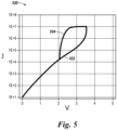
- FIG. 5 is a graph illustrating voltage and current density relationships, e.g., a JV graph, of a select device in accordance with one or more embodiments of the present disclosure.
- JV graph 520 includes line 522 that illustrates the relationship of the current density on a select device, such as select devices 108, 208, 308, 408 described in association with Figures 1-4 , when a signal, such a programming signal and/or a read signal, is applied to the select device.
- the current density on the select device starts to increase significantly once the signal reaches a threshold voltage, which is approximately 3.2 V on graph 520.
- a threshold voltage which is approximately 3.2 V on graph 520.
- the current density on the select device ranges from approximately 1E1 A/cm 2 to 1E5 A/cm 2 , when the signal is ramped from approximately 0 V to 3.5 V, while the current density on the select device ranges from approximately 1E5 A/cm 2 to 2E7 A/cm 2 , when the signal is ramped from approximately 3.2 V to 3.5 V.
- the current corresponding to the voltage ranging from 0V to 3.2 V can range from approximately 1E-10V to approximately 1E-4 V.
- the increase of the current density on the select device is caused by a drop in resistance of the select device due to the signal heating the select device having the materials and geometry described herein.
- the select devices described herein can withstand repeated heating to temperatures greater than 600°C without breaking down. For example, applying a signal that is ramped from 0 V to 3.5 V causes the select device heat up. When the select device reaches a threshold temperature (T T ) due to the voltage of the signal applied to the select device increasing, the select device snaps between resistive states and the resistance of select device decreases by a number of orders of magnitude.
- T T threshold temperature
- Figure 5 illustrates a select device that is configured to reach a threshold temperature, where the select device snaps between resistive states, which is greater than 600°C when a signal that is greater than or equal to approximately 3.2 V is applied to the select device. Once the select device snaps between resistive states and the resistance of the select device decreases, the signal is passed from the select device to a storage element of a memory cell with a magnitude of current that is sufficient to program and/or read the memory cells.
- graph 520 includes line 524 that illustrates the relationship of the current density on a select device, such as select devices 108, 208, 308, 408 described in association with Figures 1-4 , when a signal, such a programming signal and/or a read signal, is removed from the select device.
- a select device such as select devices 108, 208, 308, 408 described in association with Figures 1-4 , when a signal, such a programming signal and/or a read signal, is removed from the select device.
- line 524 on graph 520 illustrates as a signal, e.g., a first signal, having a voltage of approximately 3.5V is removed from the select device causing the voltage on the select device to decrease.
- a signal e.g., a first signal
- the temperature of select device decreases, which causes the resistance of the select device to increase and also the current density on the select device to decrease.
- the current density on the select device decreases from approximately 2E7A/cm 2 to 1E4 A/cm 2 , as the voltage of the signal decreases from approximately 3.5V to 2V.
- the decrease in current density on the select device that starts when the voltage on the select device is approximately 2V can correspond with the temperature of the select device cooling to below a threshold temperature, where the select device snaps between resistance states.
- the resistance of the select device can snap from a second resistance state to a first resistance state, where the first resistance state is a number of orders of magnitude higher than the second resistance state, when the select device cools to below the threshold temperature.
- the select device can snap between resistive states less than 15 ns after a signal is removed from the select device.
- the select device is in a resistive state where signals, e.g., a second signal, applied to the select device that are less than a threshold voltage do not pass from the select device to a storage element of a memory cell with a magnitude of current that is sufficient to program and/or read the memory cells.
- signals e.g., a second signal
- the present disclosure includes select devices and methods of using select device for memory cell applications according to independent claims 1 and 9.
Landscapes
- Engineering & Computer Science (AREA)
- Manufacturing & Machinery (AREA)
- Chemical & Material Sciences (AREA)
- Materials Engineering (AREA)
- Semiconductor Memories (AREA)
Claims (14)
- Speicherzelle, die Folgendes umfasst:
eine Auswahlvorrichtung (108, 208, 308, 408), die Folgendes enthält:eine erste Elektrode (210, 310, 410);eine erste Heizvorrichtung (314), die auf der ersten Elektrode gebildet ist;ein Halbleitermaterial (212, 312, 412), das auf der ersten Heizvorrichtung gebildet ist; eine zweite Heizvorrichtung (314), die auf dem Halbleitermaterial gebildet ist;eine zweite Elektrode (210, 310, 410) mit derselben Geometrie wie die erste Elektrode, die auf der zweiten Heizvorrichtung gebildet ist; wobeidie Auswahlvorrichtung (108, 208, 308, 408) dafür konfiguriert ist, als Reaktion auf Signale, die an die Auswahlvorrichtung (108, 208, 308, 408) angelegt werden, zwischen Widerstandszuständen überzuspringen. - Speicherzelle nach Anspruch 1, wobei das Halbleitermaterial (212, 312, 412) amorphes Silizium ist.
- Speicherzelle nach Anspruch 1, wobei die Breite des Halbleitermaterials (212, 312, 412) weniger als etwa 20 Nanometer beträgt.
- Speicherzelle nach einem der Ansprüche 1-3, wobei das Seitenverhältnis in Bezug auf eine Seitenansicht der ersten Elektrode (210, 310, 410) größer als 10 ist.
- Speicherzelle nach einem der Ansprüche 1-3, wobei die erste Elektrode (210, 310, 410) und die zweite Elektrode (210, 310, 410) optische Adsorber enthalten.
- Speicherzelle nach einem der Ansprüche 1-3, wobei das Halbleitermaterial (212, 312, 412), die erste Elektrode (210, 310, 410), und die zweite Elektrode (210, 310, 410) mit Kohlenstoff dotiert sind.
- Speicherzelle nach einem der Ansprüche 1-3, wobei die erste Elektrode (210, 310, 410) und die zweite Elektrode (210, 310, 410) aus einem Metall-/Widerstandslaminat gebildet sind.
- Speicherzelle nach Anspruch 1-3, wobei das Isolatormaterial (416) eine Dielektrizitätskonstante aufweist, die größer als 10 ist.
- Verfahren zum Betreiben einer Speicherzelle, wobei das Verfahren Folgendes umfasst:Bereitstellen eines ersten Signals an eine Auswahlvorrichtung (108, 208, 308, 408) einer Speicherzelle (105) während einer ersten Zeitperiode, wobei die Auswahlvorrichtung (108, 208, 308, 408) als Reaktion darauf, dass das Signal größer als eine Schwellenspannung ist, von einem ersten Widerstandszustand in einen zweiten Widerstandszustand überspringt,wobei die Auswahlvorrichtung Folgendes enthält:eine erste Elektrode (210, 310, 410);eine erste Heizvorrichtung (314), die auf der ersten Elektrode gebildet ist;ein Halbleitermaterial (212, 312, 412), das auf der ersten Heizvorrichtung gebildet ist;eine zweite Heizvorrichtung (314), die auf dem Halbleitermaterial gebildet ist;eine zweite Elektrode (210, 310, 410) mit derselben Geometrie wie die erste Elektrode, die auf der zweiten Heizvorrichtung gebildet ist; und Bereitstellen eines zweiten Signals an die Auswahlvorrichtung (108, 208, 308, 408) der Speicherzelle (105) während einer zweiten Zeitperiode, wobei die Auswahlvorrichtung (108, 208, 308, 408) als Reaktion auf das Signal, das kleiner als die Schwellenspannung ist, in dem ersten Widerstandszustand bleibt.
- Verfahren nach Anspruch 9, wobei das Verfahren Folgendes umfasst:
Bereitstellen einer ersten Stromdichte für ein Speicherelement (106) der Speicherzelle als Reaktion darauf, dass die Auswahlvorrichtung (108, 208, 308, 408) von dem ersten Widerstandszustand in den zweiten Widerstandszustand überspringt, und Bereitstellen einer zweiten Stromdichte für das Speicherelement (106) der Speicherzelle als Reaktion darauf, dass die Auswahlvorrichtung (108, 208, 308, 408) in dem ersten Widerstandszustand verbleibt. - Verfahren nach Anspruch 9, wobei das Verfahren das Entfernen des ersten Signals von der Auswahlvorrichtung (108, 208, 308, 408) während einer dritten Zeitspanne enthält und die Auswahlvorrichtung (108, 208, 308, 408) als Reaktion auf das Entfernen des ersten Signals von dem zweiten Widerstandszustand in den ersten Widerstandszustand überspringt.
- Verfahren nach Anspruch 11, wobei die dritte Zeitspanne weniger als 8 Nanosekunden (ns) beträgt.
- Verfahren nach Anspruch 10, wobei die erste Stromdichte größer als 1 MA/cm2 ist und die zweite Stromdichte kleiner oder gleich 1 MA/cm2 ist.
- Verfahren nach Anspruch 9, wobei das Verfahren enthält, dass die Auswahlvorrichtung (108, 208, 308, 408) während der ersten Zeitspanne eine Temperatur von mehr als 600°C erreicht.
Applications Claiming Priority (2)
| Application Number | Priority Date | Filing Date | Title |
|---|---|---|---|
| US14/515,998 US9425390B2 (en) | 2014-10-16 | 2014-10-16 | Select device for memory cell applications |
| PCT/US2015/055060 WO2016060973A1 (en) | 2014-10-16 | 2015-10-12 | Select device for memory cell applications |
Publications (3)
| Publication Number | Publication Date |
|---|---|
| EP3207575A1 EP3207575A1 (de) | 2017-08-23 |
| EP3207575A4 EP3207575A4 (de) | 2018-06-20 |
| EP3207575B1 true EP3207575B1 (de) | 2024-12-04 |
Family
ID=55747174
Family Applications (1)
| Application Number | Title | Priority Date | Filing Date |
|---|---|---|---|
| EP15850788.9A Active EP3207575B1 (de) | 2014-10-16 | 2015-10-12 | Auswahlvorrichtung für speicherzellenanwendungen |
Country Status (7)
| Country | Link |
|---|---|
| US (4) | US9425390B2 (de) |
| EP (1) | EP3207575B1 (de) |
| JP (1) | JP6552614B2 (de) |
| KR (1) | KR102001323B1 (de) |
| CN (1) | CN106796818B (de) |
| TW (1) | TWI600013B (de) |
| WO (1) | WO2016060973A1 (de) |
Families Citing this family (21)
| Publication number | Priority date | Publication date | Assignee | Title |
|---|---|---|---|---|
| US8994489B2 (en) | 2011-10-19 | 2015-03-31 | Micron Technology, Inc. | Fuses, and methods of forming and using fuses |
| US9252188B2 (en) | 2011-11-17 | 2016-02-02 | Micron Technology, Inc. | Methods of forming memory cells |
| US8723155B2 (en) * | 2011-11-17 | 2014-05-13 | Micron Technology, Inc. | Memory cells and integrated devices |
| US9553262B2 (en) | 2013-02-07 | 2017-01-24 | Micron Technology, Inc. | Arrays of memory cells and methods of forming an array of memory cells |
| US9425237B2 (en) * | 2014-03-11 | 2016-08-23 | Crossbar, Inc. | Selector device for two-terminal memory |
| US9881971B2 (en) | 2014-04-01 | 2018-01-30 | Micron Technology, Inc. | Memory arrays |
| US9362494B2 (en) | 2014-06-02 | 2016-06-07 | Micron Technology, Inc. | Array of cross point memory cells and methods of forming an array of cross point memory cells |
| US9343506B2 (en) | 2014-06-04 | 2016-05-17 | Micron Technology, Inc. | Memory arrays with polygonal memory cells having specific sidewall orientations |
| US9633724B2 (en) | 2014-07-07 | 2017-04-25 | Crossbar, Inc. | Sensing a non-volatile memory device utilizing selector device holding characteristics |
| US10211397B1 (en) | 2014-07-07 | 2019-02-19 | Crossbar, Inc. | Threshold voltage tuning for a volatile selection device |
| US10115819B2 (en) | 2015-05-29 | 2018-10-30 | Crossbar, Inc. | Recessed high voltage metal oxide semiconductor transistor for RRAM cell |
| US9460788B2 (en) | 2014-07-09 | 2016-10-04 | Crossbar, Inc. | Non-volatile memory cell utilizing volatile switching two terminal device and a MOS transistor |
| US9425390B2 (en) * | 2014-10-16 | 2016-08-23 | Micron Technology, Inc. | Select device for memory cell applications |
| US10096362B1 (en) | 2017-03-24 | 2018-10-09 | Crossbar, Inc. | Switching block configuration bit comprising a non-volatile memory cell |
| US11195839B2 (en) | 2017-09-29 | 2021-12-07 | Intel Corporation | 2S-1C 4F2 cross-point DRAM array |
| US10593399B2 (en) * | 2018-03-19 | 2020-03-17 | Micron Technology, Inc. | Self-selecting memory array with horizontal bit lines |
| CN108665926B (zh) * | 2018-04-28 | 2021-08-03 | 华中科技大学 | 一种交叉开关结构的阻变存储器写干扰优化方法 |
| US11574196B2 (en) | 2019-10-08 | 2023-02-07 | International Business Machines Corporation | Dynamic management of weight update bit length |
| JP2022144045A (ja) | 2021-03-18 | 2022-10-03 | キオクシア株式会社 | セレクタ装置及び半導体記憶装置 |
| KR20230162975A (ko) | 2021-03-30 | 2023-11-29 | 더 트러스티스 오브 더 유니버시티 오브 펜실바니아 | 재구성 가능한 인메모리 컴퓨팅을 위한 필드 프로그래밍 가능 페로 다이오드들 |
| US11894037B2 (en) * | 2022-04-12 | 2024-02-06 | Sandisk Technologies Llc | First fire and cold start in memories with threshold switching selectors |
Citations (3)
| Publication number | Priority date | Publication date | Assignee | Title |
|---|---|---|---|---|
| US20040113137A1 (en) * | 2002-12-13 | 2004-06-17 | Lowrey Tyler A. | Memory and access device and method therefor |
| US20130037776A1 (en) * | 2011-08-09 | 2013-02-14 | Kabushiki Kaisha Toshiba | Variable resistance memory |
| US20130134382A1 (en) * | 2011-11-28 | 2013-05-30 | Katholieke Universiteit Leuven, K.U. Leuven R&D | Selector Device for Memory Applications |
Family Cites Families (19)
| Publication number | Priority date | Publication date | Assignee | Title |
|---|---|---|---|---|
| UA74150C2 (uk) | 2002-01-09 | 2005-11-15 | Дженерал Електрік Компані | Спосіб формування покриття для створення теплового бар'єра та покриття для створення теплового бар'єра |
| DE60220245D1 (de) | 2002-01-17 | 2007-07-05 | St Microelectronics Srl | Integriertes Widerstandselement, Phasenwechsel Speicherelement mit solchem Widerstandselement, und Verfahren zu seiner Herstellung |
| US6891747B2 (en) | 2002-02-20 | 2005-05-10 | Stmicroelectronics S.R.L. | Phase change memory cell and manufacturing method thereof using minitrenches |
| US7646630B2 (en) | 2004-11-08 | 2010-01-12 | Ovonyx, Inc. | Programmable matrix array with chalcogenide material |
| JP2007158325A (ja) * | 2005-12-07 | 2007-06-21 | Sharp Corp | 双方向ショットキーダイオードを備えるクロスポイント型抵抗メモリ装置 |
| WO2008041303A1 (en) * | 2006-09-29 | 2008-04-10 | Fujitsu Limited | Nonvolatile semiconductor storage apparatus, reading method thereof, writing method thereof and erasing method thereof |
| US8264865B2 (en) * | 2008-07-11 | 2012-09-11 | Panasonic Corporation | Nonvolatile memory element, manufacturing method thereof, and nonvolatile semiconductor device incorporating nonvolatile memory element |
| US8227788B2 (en) | 2008-11-19 | 2012-07-24 | Panasonic Corporation | Nonvolatile memory element, and nonvolatile memory device |
| JP2013510438A (ja) | 2009-11-06 | 2013-03-21 | ラムバス・インコーポレーテッド | 三次元メモリアレイ積層構造体 |
| EP2548238B8 (de) | 2010-03-16 | 2015-06-17 | SanDisk 3D, LLC | Verfahren zur herstellung von bodenelektroden zur verwendung mit metalloxidwiderstandsschaltschichten |
| US8243506B2 (en) | 2010-08-26 | 2012-08-14 | Micron Technology, Inc. | Phase change memory structures and methods |
| US8502185B2 (en) * | 2011-05-31 | 2013-08-06 | Crossbar, Inc. | Switching device having a non-linear element |
| US8642985B2 (en) | 2011-06-30 | 2014-02-04 | Industrial Technology Research Institute | Memory Cell |
| US9142767B2 (en) | 2011-09-16 | 2015-09-22 | Micron Technology, Inc. | Resistive memory cell including integrated select device and storage element |
| US8780607B2 (en) * | 2011-09-16 | 2014-07-15 | Micron Technology, Inc. | Select devices for memory cell applications |
| US9136307B2 (en) * | 2012-02-09 | 2015-09-15 | Micron Technology, Inc. | Memory cells and memory cell formation methods using sealing material |
| US9047943B2 (en) | 2013-03-05 | 2015-06-02 | Sandisk 3D Llc | Non-volatile storage system biasing conditions for standby and first read |
| US9425390B2 (en) * | 2014-10-16 | 2016-08-23 | Micron Technology, Inc. | Select device for memory cell applications |
| US9721646B1 (en) * | 2016-06-29 | 2017-08-01 | International Business Machines Corporation | Prevention of SRAM burn-in |
-
2014
- 2014-10-16 US US14/515,998 patent/US9425390B2/en active Active
-
2015
- 2015-10-12 EP EP15850788.9A patent/EP3207575B1/de active Active
- 2015-10-12 CN CN201580055872.0A patent/CN106796818B/zh active Active
- 2015-10-12 JP JP2017519688A patent/JP6552614B2/ja active Active
- 2015-10-12 KR KR1020177012844A patent/KR102001323B1/ko active Active
- 2015-10-12 WO PCT/US2015/055060 patent/WO2016060973A1/en not_active Ceased
- 2015-10-16 TW TW104134087A patent/TWI600013B/zh active
-
2016
- 2016-07-21 US US15/215,659 patent/US9735200B2/en active Active
-
2017
- 2017-08-01 US US15/665,577 patent/US10109677B2/en active Active
-
2018
- 2018-09-06 US US16/123,073 patent/US10608048B2/en active Active
Patent Citations (3)
| Publication number | Priority date | Publication date | Assignee | Title |
|---|---|---|---|---|
| US20040113137A1 (en) * | 2002-12-13 | 2004-06-17 | Lowrey Tyler A. | Memory and access device and method therefor |
| US20130037776A1 (en) * | 2011-08-09 | 2013-02-14 | Kabushiki Kaisha Toshiba | Variable resistance memory |
| US20130134382A1 (en) * | 2011-11-28 | 2013-05-30 | Katholieke Universiteit Leuven, K.U. Leuven R&D | Selector Device for Memory Applications |
Also Published As
| Publication number | Publication date |
|---|---|
| EP3207575A1 (de) | 2017-08-23 |
| TWI600013B (zh) | 2017-09-21 |
| JP2017537463A (ja) | 2017-12-14 |
| JP6552614B2 (ja) | 2019-07-31 |
| KR102001323B1 (ko) | 2019-07-17 |
| EP3207575A4 (de) | 2018-06-20 |
| US20160329377A1 (en) | 2016-11-10 |
| US9425390B2 (en) | 2016-08-23 |
| US9735200B2 (en) | 2017-08-15 |
| CN106796818B (zh) | 2020-01-17 |
| US20170358627A1 (en) | 2017-12-14 |
| CN106796818A (zh) | 2017-05-31 |
| KR20170068559A (ko) | 2017-06-19 |
| TW201629970A (zh) | 2016-08-16 |
| WO2016060973A1 (en) | 2016-04-21 |
| US20160111639A1 (en) | 2016-04-21 |
| US20190006420A1 (en) | 2019-01-03 |
| US10608048B2 (en) | 2020-03-31 |
| US10109677B2 (en) | 2018-10-23 |
Similar Documents
| Publication | Publication Date | Title |
|---|---|---|
| EP3207575B1 (de) | Auswahlvorrichtung für speicherzellenanwendungen | |
| US8780607B2 (en) | Select devices for memory cell applications | |
| EP3440702B1 (de) | Wärmedämmung für dreidimensionale speicherarrays | |
| US7221579B2 (en) | Method and structure for high performance phase change memory | |
| CN101971264B (zh) | 具有电阻性存取组件的非易失性存储器 | |
| US9142767B2 (en) | Resistive memory cell including integrated select device and storage element | |
| US20100284213A1 (en) | Method of cross-point memory programming and related devices | |
| US10707271B2 (en) | Memory cells having resistors and formation of the same | |
| US9349445B2 (en) | Select devices for memory cell applications | |
| WO2017003960A1 (en) | Thermal management structure for low-power nonvolatile filamentary switch | |
| US9406881B1 (en) | Memory cells having a heater electrode formed between a first storage material and a second storage material and methods of forming the same | |
| WO2015134035A1 (en) | Memristor devices with a thermally-insulating cladding | |
| US9147657B2 (en) | Memory cell repair | |
| CN102185108A (zh) | 一种半导体存储器结构及其控制方法 | |
| Mei et al. | 28nm high-k metal gate RRAM with fully compatible CMOS logic processes |
Legal Events
| Date | Code | Title | Description |
|---|---|---|---|
| STAA | Information on the status of an ep patent application or granted ep patent |
Free format text: STATUS: THE INTERNATIONAL PUBLICATION HAS BEEN MADE |
|
| PUAI | Public reference made under article 153(3) epc to a published international application that has entered the european phase |
Free format text: ORIGINAL CODE: 0009012 |
|
| STAA | Information on the status of an ep patent application or granted ep patent |
Free format text: STATUS: REQUEST FOR EXAMINATION WAS MADE |
|
| 17P | Request for examination filed |
Effective date: 20170331 |
|
| AK | Designated contracting states |
Kind code of ref document: A1 Designated state(s): AL AT BE BG CH CY CZ DE DK EE ES FI FR GB GR HR HU IE IS IT LI LT LU LV MC MK MT NL NO PL PT RO RS SE SI SK SM TR |
|
| AX | Request for extension of the european patent |
Extension state: BA ME |
|
| DAV | Request for validation of the european patent (deleted) | ||
| DAX | Request for extension of the european patent (deleted) | ||
| A4 | Supplementary search report drawn up and despatched |
Effective date: 20180522 |
|
| RIC1 | Information provided on ipc code assigned before grant |
Ipc: H01L 45/02 20060101ALI20180515BHEP Ipc: H01L 45/00 20060101AFI20180515BHEP |
|
| RIC1 | Information provided on ipc code assigned before grant |
Ipc: H01L 45/00 20060101AFI20201020BHEP Ipc: H01L 27/24 20060101ALI20201020BHEP Ipc: G11C 13/00 20060101ALI20201020BHEP |
|
| STAA | Information on the status of an ep patent application or granted ep patent |
Free format text: STATUS: EXAMINATION IS IN PROGRESS |
|
| 17Q | First examination report despatched |
Effective date: 20210112 |
|
| REG | Reference to a national code |
Ref country code: DE Ref legal event code: R079 Free format text: PREVIOUS MAIN CLASS: H01L0045000000 Ipc: H10B0063000000 Ref country code: DE Ref legal event code: R079 Ref document number: 602015090579 Country of ref document: DE Free format text: PREVIOUS MAIN CLASS: H01L0045000000 Ipc: H10B0063000000 |
|
| RIC1 | Information provided on ipc code assigned before grant |
Ipc: G11C 13/00 20060101ALI20240313BHEP Ipc: H10N 70/20 20230101ALI20240313BHEP Ipc: H10N 70/00 20230101ALI20240313BHEP Ipc: H10B 61/00 20230101ALI20240313BHEP Ipc: H10B 63/00 20230101AFI20240313BHEP |
|
| GRAP | Despatch of communication of intention to grant a patent |
Free format text: ORIGINAL CODE: EPIDOSNIGR1 |
|
| STAA | Information on the status of an ep patent application or granted ep patent |
Free format text: STATUS: GRANT OF PATENT IS INTENDED |
|
| INTG | Intention to grant announced |
Effective date: 20240507 |
|
| GRAS | Grant fee paid |
Free format text: ORIGINAL CODE: EPIDOSNIGR3 |
|
| P01 | Opt-out of the competence of the unified patent court (upc) registered |
Free format text: CASE NUMBER: APP_48667/2024 Effective date: 20240826 |
|
| GRAA | (expected) grant |
Free format text: ORIGINAL CODE: 0009210 |
|
| STAA | Information on the status of an ep patent application or granted ep patent |
Free format text: STATUS: THE PATENT HAS BEEN GRANTED |
|
| AK | Designated contracting states |
Kind code of ref document: B1 Designated state(s): AL AT BE BG CH CY CZ DE DK EE ES FI FR GB GR HR HU IE IS IT LI LT LU LV MC MK MT NL NO PL PT RO RS SE SI SK SM TR |
|
| REG | Reference to a national code |
Ref country code: GB Ref legal event code: FG4D |
|
| REG | Reference to a national code |
Ref country code: CH Ref legal event code: EP |
|
| REG | Reference to a national code |
Ref country code: DE Ref legal event code: R096 Ref document number: 602015090579 Country of ref document: DE |
|
| REG | Reference to a national code |
Ref country code: IE Ref legal event code: FG4D |
|
| REG | Reference to a national code |
Ref country code: LT Ref legal event code: MG9D |
|
| REG | Reference to a national code |
Ref country code: NL Ref legal event code: MP Effective date: 20241204 |
|
| PG25 | Lapsed in a contracting state [announced via postgrant information from national office to epo] |
Ref country code: HR Free format text: LAPSE BECAUSE OF FAILURE TO SUBMIT A TRANSLATION OF THE DESCRIPTION OR TO PAY THE FEE WITHIN THE PRESCRIBED TIME-LIMIT Effective date: 20241204 |
|
| PG25 | Lapsed in a contracting state [announced via postgrant information from national office to epo] |
Ref country code: FI Free format text: LAPSE BECAUSE OF FAILURE TO SUBMIT A TRANSLATION OF THE DESCRIPTION OR TO PAY THE FEE WITHIN THE PRESCRIBED TIME-LIMIT Effective date: 20241204 |
|
| PG25 | Lapsed in a contracting state [announced via postgrant information from national office to epo] |
Ref country code: BG Free format text: LAPSE BECAUSE OF FAILURE TO SUBMIT A TRANSLATION OF THE DESCRIPTION OR TO PAY THE FEE WITHIN THE PRESCRIBED TIME-LIMIT Effective date: 20241204 |
|
| PG25 | Lapsed in a contracting state [announced via postgrant information from national office to epo] |
Ref country code: ES Free format text: LAPSE BECAUSE OF FAILURE TO SUBMIT A TRANSLATION OF THE DESCRIPTION OR TO PAY THE FEE WITHIN THE PRESCRIBED TIME-LIMIT Effective date: 20241204 |
|
| PG25 | Lapsed in a contracting state [announced via postgrant information from national office to epo] |
Ref country code: NO Free format text: LAPSE BECAUSE OF FAILURE TO SUBMIT A TRANSLATION OF THE DESCRIPTION OR TO PAY THE FEE WITHIN THE PRESCRIBED TIME-LIMIT Effective date: 20250304 |
|
| PG25 | Lapsed in a contracting state [announced via postgrant information from national office to epo] |
Ref country code: LV Free format text: LAPSE BECAUSE OF FAILURE TO SUBMIT A TRANSLATION OF THE DESCRIPTION OR TO PAY THE FEE WITHIN THE PRESCRIBED TIME-LIMIT Effective date: 20241204 Ref country code: GR Free format text: LAPSE BECAUSE OF FAILURE TO SUBMIT A TRANSLATION OF THE DESCRIPTION OR TO PAY THE FEE WITHIN THE PRESCRIBED TIME-LIMIT Effective date: 20250305 |
|
| PG25 | Lapsed in a contracting state [announced via postgrant information from national office to epo] |
Ref country code: RS Free format text: LAPSE BECAUSE OF FAILURE TO SUBMIT A TRANSLATION OF THE DESCRIPTION OR TO PAY THE FEE WITHIN THE PRESCRIBED TIME-LIMIT Effective date: 20250304 |
|
| PG25 | Lapsed in a contracting state [announced via postgrant information from national office to epo] |
Ref country code: NL Free format text: LAPSE BECAUSE OF FAILURE TO SUBMIT A TRANSLATION OF THE DESCRIPTION OR TO PAY THE FEE WITHIN THE PRESCRIBED TIME-LIMIT Effective date: 20241204 |
|
| REG | Reference to a national code |
Ref country code: AT Ref legal event code: MK05 Ref document number: 1749534 Country of ref document: AT Kind code of ref document: T Effective date: 20241204 |
|
| PG25 | Lapsed in a contracting state [announced via postgrant information from national office to epo] |
Ref country code: SM Free format text: LAPSE BECAUSE OF FAILURE TO SUBMIT A TRANSLATION OF THE DESCRIPTION OR TO PAY THE FEE WITHIN THE PRESCRIBED TIME-LIMIT Effective date: 20241204 |
|
| PG25 | Lapsed in a contracting state [announced via postgrant information from national office to epo] |
Ref country code: PL Free format text: LAPSE BECAUSE OF FAILURE TO SUBMIT A TRANSLATION OF THE DESCRIPTION OR TO PAY THE FEE WITHIN THE PRESCRIBED TIME-LIMIT Effective date: 20241204 |
|
| PG25 | Lapsed in a contracting state [announced via postgrant information from national office to epo] |
Ref country code: IS Free format text: LAPSE BECAUSE OF FAILURE TO SUBMIT A TRANSLATION OF THE DESCRIPTION OR TO PAY THE FEE WITHIN THE PRESCRIBED TIME-LIMIT Effective date: 20250404 |
|
| PG25 | Lapsed in a contracting state [announced via postgrant information from national office to epo] |
Ref country code: PT Free format text: LAPSE BECAUSE OF FAILURE TO SUBMIT A TRANSLATION OF THE DESCRIPTION OR TO PAY THE FEE WITHIN THE PRESCRIBED TIME-LIMIT Effective date: 20250404 |
|
| PG25 | Lapsed in a contracting state [announced via postgrant information from national office to epo] |
Ref country code: EE Free format text: LAPSE BECAUSE OF FAILURE TO SUBMIT A TRANSLATION OF THE DESCRIPTION OR TO PAY THE FEE WITHIN THE PRESCRIBED TIME-LIMIT Effective date: 20241204 |
|
| PG25 | Lapsed in a contracting state [announced via postgrant information from national office to epo] |
Ref country code: RO Free format text: LAPSE BECAUSE OF FAILURE TO SUBMIT A TRANSLATION OF THE DESCRIPTION OR TO PAY THE FEE WITHIN THE PRESCRIBED TIME-LIMIT Effective date: 20241204 Ref country code: AT Free format text: LAPSE BECAUSE OF FAILURE TO SUBMIT A TRANSLATION OF THE DESCRIPTION OR TO PAY THE FEE WITHIN THE PRESCRIBED TIME-LIMIT Effective date: 20241204 |
|
| PG25 | Lapsed in a contracting state [announced via postgrant information from national office to epo] |
Ref country code: SK Free format text: LAPSE BECAUSE OF FAILURE TO SUBMIT A TRANSLATION OF THE DESCRIPTION OR TO PAY THE FEE WITHIN THE PRESCRIBED TIME-LIMIT Effective date: 20241204 |
|
| PG25 | Lapsed in a contracting state [announced via postgrant information from national office to epo] |
Ref country code: CZ Free format text: LAPSE BECAUSE OF FAILURE TO SUBMIT A TRANSLATION OF THE DESCRIPTION OR TO PAY THE FEE WITHIN THE PRESCRIBED TIME-LIMIT Effective date: 20241204 |
|
| PG25 | Lapsed in a contracting state [announced via postgrant information from national office to epo] |
Ref country code: IT Free format text: LAPSE BECAUSE OF FAILURE TO SUBMIT A TRANSLATION OF THE DESCRIPTION OR TO PAY THE FEE WITHIN THE PRESCRIBED TIME-LIMIT Effective date: 20241204 |
|
| REG | Reference to a national code |
Ref country code: DE Ref legal event code: R097 Ref document number: 602015090579 Country of ref document: DE |
|
| PG25 | Lapsed in a contracting state [announced via postgrant information from national office to epo] |
Ref country code: SE Free format text: LAPSE BECAUSE OF FAILURE TO SUBMIT A TRANSLATION OF THE DESCRIPTION OR TO PAY THE FEE WITHIN THE PRESCRIBED TIME-LIMIT Effective date: 20241204 |
|
| PG25 | Lapsed in a contracting state [announced via postgrant information from national office to epo] |
Ref country code: DK Free format text: LAPSE BECAUSE OF FAILURE TO SUBMIT A TRANSLATION OF THE DESCRIPTION OR TO PAY THE FEE WITHIN THE PRESCRIBED TIME-LIMIT Effective date: 20241204 |
|
| PLBE | No opposition filed within time limit |
Free format text: ORIGINAL CODE: 0009261 |
|
| STAA | Information on the status of an ep patent application or granted ep patent |
Free format text: STATUS: NO OPPOSITION FILED WITHIN TIME LIMIT |
|
| 26N | No opposition filed |
Effective date: 20250905 |
|
| PGFP | Annual fee paid to national office [announced via postgrant information from national office to epo] |
Ref country code: DE Payment date: 20251028 Year of fee payment: 11 |
|
| PGFP | Annual fee paid to national office [announced via postgrant information from national office to epo] |
Ref country code: GB Payment date: 20251023 Year of fee payment: 11 |
|
| PGFP | Annual fee paid to national office [announced via postgrant information from national office to epo] |
Ref country code: FR Payment date: 20251027 Year of fee payment: 11 |