EP3208518A1 - Dispositif d'éclairage - Google Patents
Dispositif d'éclairage Download PDFInfo
- Publication number
- EP3208518A1 EP3208518A1 EP14904079.2A EP14904079A EP3208518A1 EP 3208518 A1 EP3208518 A1 EP 3208518A1 EP 14904079 A EP14904079 A EP 14904079A EP 3208518 A1 EP3208518 A1 EP 3208518A1
- Authority
- EP
- European Patent Office
- Prior art keywords
- globe
- lighting apparatus
- light
- optical element
- light source
- Prior art date
- Legal status (The legal status is an assumption and is not a legal conclusion. Google has not performed a legal analysis and makes no representation as to the accuracy of the status listed.)
- Pending
Links
Images


Classifications
-
- F—MECHANICAL ENGINEERING; LIGHTING; HEATING; WEAPONS; BLASTING
- F21—LIGHTING
- F21V—FUNCTIONAL FEATURES OR DETAILS OF LIGHTING DEVICES OR SYSTEMS THEREOF; STRUCTURAL COMBINATIONS OF LIGHTING DEVICES WITH OTHER ARTICLES, NOT OTHERWISE PROVIDED FOR
- F21V7/00—Reflectors for light sources
- F21V7/22—Reflectors for light sources characterised by materials, surface treatments or coatings, e.g. dichroic reflectors
- F21V7/24—Reflectors for light sources characterised by materials, surface treatments or coatings, e.g. dichroic reflectors characterised by the material
-
- F—MECHANICAL ENGINEERING; LIGHTING; HEATING; WEAPONS; BLASTING
- F21—LIGHTING
- F21K—NON-ELECTRIC LIGHT SOURCES USING LUMINESCENCE; LIGHT SOURCES USING ELECTROCHEMILUMINESCENCE; LIGHT SOURCES USING CHARGES OF COMBUSTIBLE MATERIAL; LIGHT SOURCES USING SEMICONDUCTOR DEVICES AS LIGHT-GENERATING ELEMENTS; LIGHT SOURCES NOT OTHERWISE PROVIDED FOR
- F21K9/00—Light sources using semiconductor devices as light-generating elements, e.g. using light-emitting diodes [LED] or lasers
- F21K9/20—Light sources comprising attachment means
- F21K9/23—Retrofit light sources for lighting devices with a single fitting for each light source, e.g. for substitution of incandescent lamps with bayonet or threaded fittings
- F21K9/232—Retrofit light sources for lighting devices with a single fitting for each light source, e.g. for substitution of incandescent lamps with bayonet or threaded fittings specially adapted for generating an essentially omnidirectional light distribution, e.g. with a glass bulb
-
- F—MECHANICAL ENGINEERING; LIGHTING; HEATING; WEAPONS; BLASTING
- F21—LIGHTING
- F21K—NON-ELECTRIC LIGHT SOURCES USING LUMINESCENCE; LIGHT SOURCES USING ELECTROCHEMILUMINESCENCE; LIGHT SOURCES USING CHARGES OF COMBUSTIBLE MATERIAL; LIGHT SOURCES USING SEMICONDUCTOR DEVICES AS LIGHT-GENERATING ELEMENTS; LIGHT SOURCES NOT OTHERWISE PROVIDED FOR
- F21K9/00—Light sources using semiconductor devices as light-generating elements, e.g. using light-emitting diodes [LED] or lasers
- F21K9/60—Optical arrangements integrated in the light source, e.g. for improving the colour rendering index or the light extraction
- F21K9/61—Optical arrangements integrated in the light source, e.g. for improving the colour rendering index or the light extraction using light guides
-
- F—MECHANICAL ENGINEERING; LIGHTING; HEATING; WEAPONS; BLASTING
- F21—LIGHTING
- F21S—NON-PORTABLE LIGHTING DEVICES; SYSTEMS THEREOF; VEHICLE LIGHTING DEVICES SPECIALLY ADAPTED FOR VEHICLE EXTERIORS
- F21S2/00—Systems of lighting devices, not provided for in main groups F21S4/00 - F21S10/00 or F21S19/00, e.g. of modular construction
-
- F—MECHANICAL ENGINEERING; LIGHTING; HEATING; WEAPONS; BLASTING
- F21—LIGHTING
- F21Y—INDEXING SCHEME ASSOCIATED WITH SUBCLASSES F21K, F21L, F21S and F21V, RELATING TO THE FORM OR THE KIND OF THE LIGHT SOURCES OR OF THE COLOUR OF THE LIGHT EMITTED
- F21Y2115/00—Light-generating elements of semiconductor light sources
- F21Y2115/10—Light-emitting diodes [LED]
Definitions
- Embodiments of the present invention relate generally to a lighting apparatus used in ordinary households, shops, and offices.
- LED lighting apparatuses for ordinary lighting may be required to achieve (retrofit) a shape and a way of lighting close to those of incandescent light bulbs.
- incandescent light bulbs there have been demands for lighting with wide light distribution (1/2 light distribution angle is substantially 270°) from a point light source inside the globe, like clear type incandescent light bulbs (light bulbs using a clear glass globe).
- PATENT LITERATURE 1 US Patent Application Publication No. 2010/0308354
- the light distribution angle is narrowed, and the 1/2 light distribution angle is substantially 120°.
- a lighting apparatus includes a globe, an optical element including a scattering portion inside and transparent to visible light, and a light source disposed to be opposed to a light incident surface of the optical element.
- the scattering portion is disposed inside the globe.
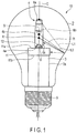
- FIG. 1 is a schematic diagram illustrating a lighting apparatus 10 according to a first embodiment.
- the lighting apparatus 10 has a rotation-symmetrical shape with respect to a central axis C.
- the lighting apparatus 10 includes a transparent globe 2 of an ordinary bulb type, an optical element 4 formed of a material (acryl in the present embodiment) transparent to visible light, and a light source 6 disposed to be opposed to a light incident surface 4a of the optical element 4 described later.
- the lighting apparatus 10 also includes a diffusion portion 3 supporting a substrate 11 including the light source 6, and a base 5 connected with an opening end of the globe 2.
- the optical element 4, the light source 6, the substrate 11, and the diffusion portion 3 are disposed inside the globe 2.
- the globe 2 includes a surface including an R curved surface.
- the R curved surface means a curved surface that secures a fixed point having a fixed distance from each of successive points on the curved surface.
- the fixed point serves as the center of the globe 2.
- the R curved surface may include a spherical surface, but the surface shape of the globe 2 is not limited to a spherical surface.
- the globe 2 has a rotation-symmetrical shape with respect to the central axis thereof.
- the rotation-symmetrical shape means a shape in which the object agrees with the original shape when the object is rotated with respect to the central axis C, and the rotational angle around the central axis C is less than 360°.
- Examples of the object of a rotation-symmetrical shape include a column, a cone, a polygonal prism, and a polygonal pyramid.
- the optical element 4 has a rotation-symmetrical shape with respect to the central axis C, and has a substantially cylindrical shape in the present embodiment.
- the material of the optical element 4 may be any material as long as the material is transparent to visible light.
- the optical element 4 may be formed of, for example, polycarbonate or glass, as well as acryl.
- the optical element 4 is disposed coaxially with the globe 2. Specifically, the central axis (first rotation-symmetrical axis) of the optical element 4 agrees with the central axis (second rotation-symmetrical axis) of the globe 2.
- the optical element 4 includes a scattering portion 8 serving as a cavity in which the transparent material does not exist.
- the scattering portion 8 also has a rotation-symmetrical shape with respect to the central axis C.
- the scattering portion 8 is a recessed portion including an opening portion 8a at a distal end (upper end in the drawing) of the optical element 4 and apart from the light source 6.
- the scattering portion 8 has a length substantially half the whole longitudinal length of the optical element 4.
- a bottom portion of the scattering portion 8 on the light source 6 side (lower end side in the drawing) gradually converges toward the central axis C and is closed.
- the scattering portion 8 is disposed inside the globe 2.
- the internal surface of the scattering portion 8 serves as a diffusion surface 8b to diffuse light.
- the diffusion surface 8b may be formed by painting the internal surface of the scattering portion 8 white. Otherwise, the diffusion surface 8b may be a rough surface obtained by subjecting part of the internal surface of the scattering portion 8 to sandblasting. Instead of providing the diffusion surface 8b, a scattering member (not illustrated) to scatter light may be filled into the scattering portion 8.
- the optical element 4 includes a light incident surface 4a at a proximal end portion thereof distant from the opening portion 8a of the scattering portion 8.
- the light incident surface 4a is a recessed portion recessed in a spherical shape from the proximal end portion of the optical element 4.
- a light emitting surface 6a of the light source 6 is opposed to the recessed portion 4a.
- the optical element 4 also includes an external circumferential surface 4b that is gradually reduced in diameter toward the distal end.
- the external circumferential surface 4b with a reduced diameter is connected with the opening portion 8a of the scattering portion 8 at the distal end of the optical element 4.
- the external circumferential surface 4b is a mirror surface.
- the light source 6 includes an LED device (not illustrated) mounted on a surface 11a of the substrate 11, and a sealing resin 12 sealing the LED device on the surface 11a of the substrate 11.
- White paint is applied to the surface 11a of the substrate 11, to diffuse and reflect light.
- the sealing resin 12 has a substantially hemispherical shape, and a surface of the sealing resin 12 functions as the light emitting surface 6a.
- the light source 6 is attached to the diffusion portion 3, by supporting a back surface 11b of the substrate 11 with the diffusion portion 3. In this state, the light emitting surface 6a is opposed to the light incident surface 4a of the optical element 4.
- the diffusion portion 3 is formed of a metal material, and thermally contacts the back surface 11b of the substrate 11. Specifically, the diffusion portion 3 thermally contacts the light source 6 through the substrate 11, to diffuse and radiate the heat of the light source 6.
- the diffusion portion 3 also includes a surface 3a subjected to surface treatment to diffuse and reflect light. For example, white paint is applied to the surface 3a of the diffusion portion 3.
- the scattering portion 8 is disposed opposite to the light source 6 with respect to the center R of the globe 2.
- the scattering portion 8 is disposed such that the end portion thereof on the light source 6 side is positioned in the center R of the globe 2, as illustrated in FIG. 2 .
- the position of the scattering portion 8 along the central axis C can be changed by adjusting, for example, the length of the diffusion portion 3 in the axial direction.
- Rays emitted from the light source 6 through the light emitting surface 6a are made incident on the light incident surface 4a of the optical element 4.
- the light made incident on the optical element 4 through the light incident surface 4a is guided through the optical element 4, and diffused and reflected in the scattering portion 8.
- the light diffused and reflected in the scattering portion 8 spreads in substantially all directions, and is emitted to the outside of the optical element 4 by refraction and transmission. As described above, most of light emitted from the optical element 4 is transmitted through the globe 2, and used as illumination light.
- the incident angle of light herein means an angle between a normal H running through a point at which light is made incident on the internal surface of the globe 2 and a ray made incident on the point.
- a ray L1 indicated with a broken line arrow in FIG. 1 indicates a ray scattered by an end portion of the scattering portion 8 distant from the light source 6.
- the ray L1 is reflected by the internal surface of the globe 2, and goes toward the substrate 11 and/or the diffusion portion 3.
- the direction in which the ray L1 is reflected is a direction close to the base 5 beyond the center R of the globe 2.
- the direction in which the ray L1 is reflected is a direction opposite to a direction of going toward the top portion that is most distant from the base 5 of the globe 2.
- the ray L1 reflected in this direction is further reflected by the surface of the substrate 11 and/or the surface of the diffusion portion 3, and serves as an optical component to cause the illumination light to have wide light distribution.
- a ray L2 indicated with a solid line arrow in FIG. 1 indicates a ray scattered by an end portion of the scattering portion 8 close to the light source 6.
- the ray L2 is reflected by the internal surface of the globe 2, and goes toward the optical element 4.
- the direction in which the ray L2 is reflected is a direction close to the base 5 beyond the center R of the globe 2.
- the ray L2 reflected in this direction is reflected by the surface of the optical element 4, or transmitted through the optical element 4.
- the scattering portion 8 when the scattering portion 8 is disposed on a side opposite to the light source 6 with respect to the center R of the globe 2, the ray L1 and the ray L2 are reflected in the direction close to the base 5 beyond the center R of the globe 2, and hit against any of the optical element 4, the substrate 11, and the diffusion portion 3.
- the ray that has reached the substrate 11 and/or the diffusion portion 3 is diffused and reflected in a direction going toward the base 5.
- the optical element 4 provided as in the present embodiment enables scattering of rays emitted from the light source 6 with the scattering portion 8, enables generation of wide light distribution components, and causes illumination light emitted from the globe 2 to have wide light distribution.
- the condition for emitting illumination light with wide light distribution as described above is to provide the scattering portion 8 inside the globe 2.
- the scattering portion 8 is disposed on a side opposite to the light source 6 with respect to the center R of the globe 2.
- the light component reflected by the internal surface of the globe 2 by Fresnel reflection without being transmitted through the globe 2 goes toward the direction of the base 5.
- part of the light reflected by the internal surface of the globe 2 is further reflected by the surface of the substrate 11 and/or the surface of the diffusion portion 3, to serve as wide light distribution components in the end, and is emitted from the globe 2. For this reason, these optical components serve as optical components to cause the illumination light to have wide light distribution.
- Fresnel reflection components in the internal surface of the globe can be converted into wide light distribution components.
- This structure achieves an LED light bulb with wider light distribution, and enables emission of light with wide light distribution and retrofitting property.
- the center R of the globe 2 is required to be positioned within a line segment connecting the scattering portion 8 of the optical element 4 with the light source 6, at the optical element 4 outside the scattering portion 8 or close to the light source 6.
- the ray L1 has the maximum incident angle, among the rays scattered in the scattering portion 8. When the center R of the globe 2 is positioned at an end portion of the scattering portion 8 on a side close to the light source 6, the incident angle of the ray L1 becomes minimum. Specifically, in this state, the luminaire efficiency becomes maximum.
- the lighting apparatus 20 according to the present embodiment has a structure similar to that of the lighting apparatus 10 according to the first embodiment described above, except that the position of the scattering portion 8 along the central axis C is changed. Accordingly, constituent elements functioning similarly to those of the first embodiment are denoted by the same reference numerals, and detailed explanation thereof is omitted.
- the scattering portion 8 of the lighting apparatus 20 is disposed in a position including the center R of the globe 2. More preferably, the scattering portion 8 is disposed such that the center of the scattering portion 8 overlaps with the center R of the globe 2.
- Fresnel reflection components in the internal surface of the globe 2 are absorbed by the optical element 4, the substrate 11, or the diffusion portion 3. For this reason, Fresnel reflection should be suppressed as much as possible in view of the luminaire efficiency.
- Fresnel reflection components increase as the incident angle of light with respect to the internal surface of the globe 2 increases. For this reason, the incident angle should be reduced as much as possible.
- the ray that has the maximum incident angle with respect to the internal surface of the globe 2 is the ray L1 scattered at the end portion of the scattering portion 8 distant from the light source 6, or the ray L2 scattered at the end portion of the scattering portion 8 close to the light source 6.
- the center R of the globe 2 is located in a position of the scattering portion 8 obtained by dividing the length of the scattering portion 8 along the central axis C in half, the maximum values of the incident angles of the rays L1 and L2 become minimum. This structure minimizes Fresnel reflection components, and reduces reflection loss.
- the present embodiment increases optical components in a direction of going toward the base 5, with reflection loss in the internal surface of the globe 2 suppressed to the minimum, and enables emission of light with wide light distribution and retrofitting property.
- the lighting apparatus 30 according to the present embodiment has a structure similar to that of the lighting apparatus 10 according to the first embodiment described above, except that the position of the scattering portion 8 along the central axis C is changed. Accordingly, constituent elements functioning similarly to those of the first embodiment are denoted by the same reference numerals, and detailed explanation thereof is omitted.
- the scattering portion 8 of the lighting apparatus 30 is disposed in a position on the light source 6 side beyond the center R of the globe 2. More preferably, the scattering portion 8 is disposed such that the end portion of the scattering portion 8 on a side opposite to the light source 6 is disposed in the center R of the globe 2.
- the ray that has the maximum incident angle with respect to the internal surface of the globe 2 is the ray L2 scattered at the end portion of the scattering portion 8 close to the light source 6, among the rays scattered in the scattering portion 8.
- the ray that has the minimum incident angle with respect to the internal surface of the globe 2 is the ray L1 scattered at the end portion of the scattering portion 8 distant from the light source 6.
- All the reflection components of the rays L1 and L2 in the internal surface of the globe 2 go in a direction (that is, a direction going away from the light source 6) toward the top portion of the globe 2. Specifically, rays reflected by the internal surface of the globe 2 do not go toward the optical element 4, the substrate 11, or the diffusion portion 3. This structure increases narrow-angle components, and produces shine in the top portion of the globe 2.
- Fresnel reflection should be suppressed as much as possible, and the center R of the globe 2 should be located in an end portion of the scattering portion 8 distant from the light source 6.
- the substrate 11, or the diffusion portion 3 because rays reflected by the internal surface of the globe 2 do not go toward the optical element 4, the substrate 11, or the diffusion portion 3, the rays are not absorbed, and loss is reduced.
- the present embodiment reduces absorption loss of rays in the optical element 4, the substrate 11, or the diffusion portion 3, increases narrow-angle components, while wide light distribution is maintained with the optical element 4, and achieves a light bulb with a bright top portion of the globe 2.
- FIG. 5 is a schematic diagram illustrating a lighting apparatus 40 according to a fourth embodiment
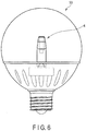
- FIG. 6 is a schematic diagram illustrating a lighting apparatus 50 according to a fifth embodiment.
- the lighting apparatus 40 in FIG. 5 is a light bulb of a chandelier bulb type
- the lighting apparatus 50 in FIG. 6 is a light bulb of a ball bulb type.
- the first to the third embodiments described above illustrate light bulbs of an ordinary bulb type, but the present invention is also applicable to light bulbs of the chandelier bulb type and the ball bulb type.
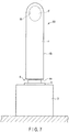
- FIG. 7 is a schematic diagram illustrating a modification of the optical element 4 incorporated in the lighting apparatuses according to the first to the fifth embodiments described above.
- An optical element 60 according to the modification has a structure similar to that of the optical element 4 described above, except that the optical element 60 includes a flat light incident surface 61 and a scattering portion 62 being a cavity of a rotation oval shape. Accordingly, constituent elements functioning similarly to those of the optical element 4 are denoted by the same reference numerals, and detailed explanation thereof is omitted.
- the shape of the scattering portion 62 is not limited to a recessed portion opened to the distal end of the optical element or a rotation oval shape, but various shapes may be selected, such as a spherical shape, and a recessed portion opened to the proximal end of the optical element. In any case, any scattering portion may be used as long as the scattering portion has a rotation-symmetrical shape with respect to the central axis of the optical element.
Landscapes
- Engineering & Computer Science (AREA)
- General Engineering & Computer Science (AREA)
- Physics & Mathematics (AREA)
- Microelectronics & Electronic Packaging (AREA)
- Optics & Photonics (AREA)
- Non-Portable Lighting Devices Or Systems Thereof (AREA)
- Optical Elements Other Than Lenses (AREA)
- Planar Illumination Modules (AREA)
- Led Device Packages (AREA)
Applications Claiming Priority (1)
| Application Number | Priority Date | Filing Date | Title |
|---|---|---|---|
| PCT/JP2014/077456 WO2016059687A1 (fr) | 2014-10-15 | 2014-10-15 | Dispositif d'éclairage |
Publications (2)
| Publication Number | Publication Date |
|---|---|
| EP3208518A1 true EP3208518A1 (fr) | 2017-08-23 |
| EP3208518A4 EP3208518A4 (fr) | 2018-04-11 |
Family
ID=55746257
Family Applications (1)
| Application Number | Title | Priority Date | Filing Date |
|---|---|---|---|
| EP14904079.2A Pending EP3208518A4 (fr) | 2014-10-15 | 2014-10-15 | Dispositif d'éclairage |
Country Status (5)
| Country | Link |
|---|---|
| US (1) | US10107457B2 (fr) |
| EP (1) | EP3208518A4 (fr) |
| JP (1) | JPWO2016059687A1 (fr) |
| CN (1) | CN106662299A (fr) |
| WO (1) | WO2016059687A1 (fr) |
Families Citing this family (2)
| Publication number | Priority date | Publication date | Assignee | Title |
|---|---|---|---|---|
| JP6867606B2 (ja) * | 2017-06-15 | 2021-04-28 | 東芝ライテック株式会社 | 照明装置 |
| JP7618896B2 (ja) | 2021-11-25 | 2025-01-21 | シグニファイ ホールディング ビー ヴィ | 光ガイドランプ |
Family Cites Families (18)
| Publication number | Priority date | Publication date | Assignee | Title |
|---|---|---|---|---|
| US6350041B1 (en) | 1999-12-03 | 2002-02-26 | Cree Lighting Company | High output radial dispersing lamp using a solid state light source |
| US6736526B2 (en) * | 2001-03-27 | 2004-05-18 | Matsushita Electric Industrial Co., Ltd. | Bulb-type lamp and manufacturing method for the bulb-type lamp |
| US8628220B2 (en) | 2009-01-09 | 2014-01-14 | Koninklijke Philips N.V. | Light source |
| JP5363864B2 (ja) * | 2009-04-13 | 2013-12-11 | 日東光学株式会社 | 発光装置および電球型ledランプ |
| US8168998B2 (en) | 2009-06-09 | 2012-05-01 | Koninklijke Philips Electronics N.V. | LED with remote phosphor layer and reflective submount |
| US8482186B2 (en) * | 2010-05-03 | 2013-07-09 | Young Lighting Technology Inc. | Lighting device |
| JP5330420B2 (ja) * | 2011-01-24 | 2013-10-30 | 株式会社サンテック | Led電球 |
| JP5178930B1 (ja) | 2011-03-11 | 2013-04-10 | 株式会社東芝 | 照明装置 |
| JP5010751B1 (ja) | 2011-03-11 | 2012-08-29 | 株式会社東芝 | 照明装置 |
| TWM429802U (en) * | 2011-09-30 | 2012-05-21 | Chicony Power Tech Co Ltd | Light source module and light-emitting device thereof |
| TWI465672B (zh) * | 2012-02-14 | 2014-12-21 | 財團法人工業技術研究院 | 照明裝置 |
| JP2013200963A (ja) * | 2012-03-23 | 2013-10-03 | Harison Toshiba Lighting Corp | 半導体光源および照明装置 |
| JP2014060086A (ja) * | 2012-09-19 | 2014-04-03 | Beat Sonic:Kk | Ledランプ |
| JP6045864B2 (ja) | 2012-09-20 | 2016-12-14 | 株式会社東芝 | Led照明装置 |
| US9677738B2 (en) * | 2013-03-15 | 2017-06-13 | 1947796 Ontario Inc. | Optical device and system for solid-state lighting |
| JP6013977B2 (ja) | 2013-06-11 | 2016-10-25 | 株式会社東芝 | 照明装置および光ガイド |
| JPWO2016051523A1 (ja) * | 2014-09-30 | 2017-04-27 | 株式会社東芝 | 光学素子および照明装置 |
| US9609761B2 (en) * | 2014-10-03 | 2017-03-28 | Hung-Chang Chen | Method of mounting self-adhesive substrate on electronic device |
-
2014
- 2014-10-15 EP EP14904079.2A patent/EP3208518A4/fr active Pending
- 2014-10-15 WO PCT/JP2014/077456 patent/WO2016059687A1/fr not_active Ceased
- 2014-10-15 CN CN201480080935.3A patent/CN106662299A/zh active Pending
- 2014-10-15 JP JP2016553914A patent/JPWO2016059687A1/ja not_active Abandoned
-
2017
- 2017-04-07 US US15/482,093 patent/US10107457B2/en active Active
Also Published As
| Publication number | Publication date |
|---|---|
| CN106662299A (zh) | 2017-05-10 |
| WO2016059687A1 (fr) | 2016-04-21 |
| EP3208518A4 (fr) | 2018-04-11 |
| US10107457B2 (en) | 2018-10-23 |
| US20170211749A1 (en) | 2017-07-27 |
| JPWO2016059687A1 (ja) | 2017-06-01 |
Similar Documents
| Publication | Publication Date | Title |
|---|---|---|
| US8628220B2 (en) | Light source | |
| US8292471B2 (en) | Light source | |
| US8602621B2 (en) | Optical element and light source comprising the same | |
| CN103649630A (zh) | 光导 | |
| TW201523033A (zh) | 全向發光二極體透鏡 | |
| US10107457B2 (en) | Lighting apparatus | |
| EP3203144B1 (fr) | Élément optique et dispositif d'éclairage | |
| JP6763047B2 (ja) | 照明装置 | |
| JP2019050208A (ja) | 光学素子および照明装置 | |
| US9506624B2 (en) | Lamp having lens element for distributing light | |
| KR20150102434A (ko) | 엘이디 조명 기구 | |
| TW201323769A (zh) | 發光二極體燈具 | |
| KR20170102082A (ko) | 전구형 엘이디 조명장치 |
Legal Events
| Date | Code | Title | Description |
|---|---|---|---|
| STAA | Information on the status of an ep patent application or granted ep patent |
Free format text: STATUS: THE INTERNATIONAL PUBLICATION HAS BEEN MADE |
|
| PUAI | Public reference made under article 153(3) epc to a published international application that has entered the european phase |
Free format text: ORIGINAL CODE: 0009012 |
|
| STAA | Information on the status of an ep patent application or granted ep patent |
Free format text: STATUS: REQUEST FOR EXAMINATION WAS MADE |
|
| 17P | Request for examination filed |
Effective date: 20170330 |
|
| AK | Designated contracting states |
Kind code of ref document: A1 Designated state(s): AL AT BE BG CH CY CZ DE DK EE ES FI FR GB GR HR HU IE IS IT LI LT LU LV MC MK MT NL NO PL PT RO RS SE SI SK SM TR |
|
| AX | Request for extension of the european patent |
Extension state: BA ME |
|
| DAX | Request for extension of the european patent (deleted) | ||
| A4 | Supplementary search report drawn up and despatched |
Effective date: 20180309 |
|
| RIC1 | Information provided on ipc code assigned before grant |
Ipc: F21Y 101/00 20160101ALI20180306BHEP Ipc: F21V 8/00 20060101ALI20180306BHEP Ipc: F21S 2/00 20160101AFI20180306BHEP |
|
| STAA | Information on the status of an ep patent application or granted ep patent |
Free format text: STATUS: EXAMINATION IS IN PROGRESS |
|
| 17Q | First examination report despatched |
Effective date: 20190626 |
|
| RAP1 | Party data changed (applicant data changed or rights of an application transferred) |
Owner name: KABUSHIKI KAISHA TOSHIBA |
|
| GRAP | Despatch of communication of intention to grant a patent |
Free format text: ORIGINAL CODE: EPIDOSNIGR1 |
|
| STAA | Information on the status of an ep patent application or granted ep patent |
Free format text: STATUS: GRANT OF PATENT IS INTENDED |