EP3208791B1 - Anzeigeschaltung und ansteuerungsverfahren dafür sowie anzeigevorrichtung - Google Patents
Anzeigeschaltung und ansteuerungsverfahren dafür sowie anzeigevorrichtung Download PDFInfo
- Publication number
- EP3208791B1 EP3208791B1 EP15775602.4A EP15775602A EP3208791B1 EP 3208791 B1 EP3208791 B1 EP 3208791B1 EP 15775602 A EP15775602 A EP 15775602A EP 3208791 B1 EP3208791 B1 EP 3208791B1
- Authority
- EP
- European Patent Office
- Prior art keywords
- terminal
- unit
- node
- signal
- output
- Prior art date
- Legal status (The legal status is an assumption and is not a legal conclusion. Google has not performed a legal analysis and makes no representation as to the accuracy of the status listed.)
- Active
Links
Images




Classifications
-
- G—PHYSICS
- G09—EDUCATION; CRYPTOGRAPHY; DISPLAY; ADVERTISING; SEALS
- G09G—ARRANGEMENTS OR CIRCUITS FOR CONTROL OF INDICATING DEVICES USING STATIC MEANS TO PRESENT VARIABLE INFORMATION
- G09G5/00—Control arrangements or circuits for visual indicators common to cathode-ray tube indicators and other visual indicators
- G09G5/10—Intensity circuits
-
- G—PHYSICS
- G09—EDUCATION; CRYPTOGRAPHY; DISPLAY; ADVERTISING; SEALS
- G09G—ARRANGEMENTS OR CIRCUITS FOR CONTROL OF INDICATING DEVICES USING STATIC MEANS TO PRESENT VARIABLE INFORMATION
- G09G3/00—Control arrangements or circuits, of interest only in connection with visual indicators other than cathode-ray tubes
- G09G3/20—Control arrangements or circuits, of interest only in connection with visual indicators other than cathode-ray tubes for presentation of an assembly of a number of characters, e.g. a page, by composing the assembly by combination of individual elements arranged in a matrix no fixed position being assigned to or needed to be assigned to the individual characters or partial characters
- G09G3/22—Control arrangements or circuits, of interest only in connection with visual indicators other than cathode-ray tubes for presentation of an assembly of a number of characters, e.g. a page, by composing the assembly by combination of individual elements arranged in a matrix no fixed position being assigned to or needed to be assigned to the individual characters or partial characters using controlled light sources
- G09G3/30—Control arrangements or circuits, of interest only in connection with visual indicators other than cathode-ray tubes for presentation of an assembly of a number of characters, e.g. a page, by composing the assembly by combination of individual elements arranged in a matrix no fixed position being assigned to or needed to be assigned to the individual characters or partial characters using controlled light sources using electroluminescent panels
- G09G3/32—Control arrangements or circuits, of interest only in connection with visual indicators other than cathode-ray tubes for presentation of an assembly of a number of characters, e.g. a page, by composing the assembly by combination of individual elements arranged in a matrix no fixed position being assigned to or needed to be assigned to the individual characters or partial characters using controlled light sources using electroluminescent panels semiconductive, e.g. using light-emitting diodes [LED]
- G09G3/3208—Control arrangements or circuits, of interest only in connection with visual indicators other than cathode-ray tubes for presentation of an assembly of a number of characters, e.g. a page, by composing the assembly by combination of individual elements arranged in a matrix no fixed position being assigned to or needed to be assigned to the individual characters or partial characters using controlled light sources using electroluminescent panels semiconductive, e.g. using light-emitting diodes [LED] organic, e.g. using organic light-emitting diodes [OLED]
- G09G3/3266—Details of drivers for scan electrodes
-
- G—PHYSICS
- G09—EDUCATION; CRYPTOGRAPHY; DISPLAY; ADVERTISING; SEALS
- G09G—ARRANGEMENTS OR CIRCUITS FOR CONTROL OF INDICATING DEVICES USING STATIC MEANS TO PRESENT VARIABLE INFORMATION
- G09G3/00—Control arrangements or circuits, of interest only in connection with visual indicators other than cathode-ray tubes
- G09G3/20—Control arrangements or circuits, of interest only in connection with visual indicators other than cathode-ray tubes for presentation of an assembly of a number of characters, e.g. a page, by composing the assembly by combination of individual elements arranged in a matrix no fixed position being assigned to or needed to be assigned to the individual characters or partial characters
- G09G3/22—Control arrangements or circuits, of interest only in connection with visual indicators other than cathode-ray tubes for presentation of an assembly of a number of characters, e.g. a page, by composing the assembly by combination of individual elements arranged in a matrix no fixed position being assigned to or needed to be assigned to the individual characters or partial characters using controlled light sources
- G09G3/30—Control arrangements or circuits, of interest only in connection with visual indicators other than cathode-ray tubes for presentation of an assembly of a number of characters, e.g. a page, by composing the assembly by combination of individual elements arranged in a matrix no fixed position being assigned to or needed to be assigned to the individual characters or partial characters using controlled light sources using electroluminescent panels
- G09G3/32—Control arrangements or circuits, of interest only in connection with visual indicators other than cathode-ray tubes for presentation of an assembly of a number of characters, e.g. a page, by composing the assembly by combination of individual elements arranged in a matrix no fixed position being assigned to or needed to be assigned to the individual characters or partial characters using controlled light sources using electroluminescent panels semiconductive, e.g. using light-emitting diodes [LED]
- G09G3/3208—Control arrangements or circuits, of interest only in connection with visual indicators other than cathode-ray tubes for presentation of an assembly of a number of characters, e.g. a page, by composing the assembly by combination of individual elements arranged in a matrix no fixed position being assigned to or needed to be assigned to the individual characters or partial characters using controlled light sources using electroluminescent panels semiconductive, e.g. using light-emitting diodes [LED] organic, e.g. using organic light-emitting diodes [OLED]
- G09G3/3225—Control arrangements or circuits, of interest only in connection with visual indicators other than cathode-ray tubes for presentation of an assembly of a number of characters, e.g. a page, by composing the assembly by combination of individual elements arranged in a matrix no fixed position being assigned to or needed to be assigned to the individual characters or partial characters using controlled light sources using electroluminescent panels semiconductive, e.g. using light-emitting diodes [LED] organic, e.g. using organic light-emitting diodes [OLED] using an active matrix
- G09G3/3258—Control arrangements or circuits, of interest only in connection with visual indicators other than cathode-ray tubes for presentation of an assembly of a number of characters, e.g. a page, by composing the assembly by combination of individual elements arranged in a matrix no fixed position being assigned to or needed to be assigned to the individual characters or partial characters using controlled light sources using electroluminescent panels semiconductive, e.g. using light-emitting diodes [LED] organic, e.g. using organic light-emitting diodes [OLED] using an active matrix with pixel circuitry controlling the voltage across the light-emitting element
-
- G—PHYSICS
- G11—INFORMATION STORAGE
- G11C—STATIC STORES
- G11C19/00—Digital stores in which the information is moved stepwise, e.g. shift registers
- G11C19/28—Digital stores in which the information is moved stepwise, e.g. shift registers using semiconductor elements
- G11C19/287—Organisation of a multiplicity of shift registers
-
- G—PHYSICS
- G09—EDUCATION; CRYPTOGRAPHY; DISPLAY; ADVERTISING; SEALS
- G09G—ARRANGEMENTS OR CIRCUITS FOR CONTROL OF INDICATING DEVICES USING STATIC MEANS TO PRESENT VARIABLE INFORMATION
- G09G2300/00—Aspects of the constitution of display devices
- G09G2300/04—Structural and physical details of display devices
- G09G2300/0404—Matrix technologies
- G09G2300/0408—Integration of the drivers onto the display substrate
-
- G—PHYSICS
- G09—EDUCATION; CRYPTOGRAPHY; DISPLAY; ADVERTISING; SEALS
- G09G—ARRANGEMENTS OR CIRCUITS FOR CONTROL OF INDICATING DEVICES USING STATIC MEANS TO PRESENT VARIABLE INFORMATION
- G09G2310/00—Command of the display device
- G09G2310/02—Addressing, scanning or driving the display screen or processing steps related thereto
- G09G2310/0262—The addressing of the pixel, in a display other than an active matrix LCD, involving the control of two or more scan electrodes or two or more data electrodes, e.g. pixel voltage dependent on signals of two data electrodes
-
- G—PHYSICS
- G09—EDUCATION; CRYPTOGRAPHY; DISPLAY; ADVERTISING; SEALS
- G09G—ARRANGEMENTS OR CIRCUITS FOR CONTROL OF INDICATING DEVICES USING STATIC MEANS TO PRESENT VARIABLE INFORMATION
- G09G2310/00—Command of the display device
- G09G2310/02—Addressing, scanning or driving the display screen or processing steps related thereto
- G09G2310/0264—Details of driving circuits
- G09G2310/0286—Details of a shift registers arranged for use in a driving circuit
-
- G—PHYSICS
- G09—EDUCATION; CRYPTOGRAPHY; DISPLAY; ADVERTISING; SEALS
- G09G—ARRANGEMENTS OR CIRCUITS FOR CONTROL OF INDICATING DEVICES USING STATIC MEANS TO PRESENT VARIABLE INFORMATION
- G09G2310/00—Command of the display device
- G09G2310/06—Details of flat display driving waveforms
- G09G2310/061—Details of flat display driving waveforms for resetting or blanking
-
- G—PHYSICS
- G09—EDUCATION; CRYPTOGRAPHY; DISPLAY; ADVERTISING; SEALS
- G09G—ARRANGEMENTS OR CIRCUITS FOR CONTROL OF INDICATING DEVICES USING STATIC MEANS TO PRESENT VARIABLE INFORMATION
- G09G2310/00—Command of the display device
- G09G2310/08—Details of timing specific for flat panels, other than clock recovery
-
- G—PHYSICS
- G09—EDUCATION; CRYPTOGRAPHY; DISPLAY; ADVERTISING; SEALS
- G09G—ARRANGEMENTS OR CIRCUITS FOR CONTROL OF INDICATING DEVICES USING STATIC MEANS TO PRESENT VARIABLE INFORMATION
- G09G2320/00—Control of display operating conditions
- G09G2320/04—Maintaining the quality of display appearance
- G09G2320/043—Preventing or counteracting the effects of ageing
-
- G—PHYSICS
- G09—EDUCATION; CRYPTOGRAPHY; DISPLAY; ADVERTISING; SEALS
- G09G—ARRANGEMENTS OR CIRCUITS FOR CONTROL OF INDICATING DEVICES USING STATIC MEANS TO PRESENT VARIABLE INFORMATION
- G09G2320/00—Control of display operating conditions
- G09G2320/04—Maintaining the quality of display appearance
- G09G2320/043—Preventing or counteracting the effects of ageing
- G09G2320/045—Compensation of drifts in the characteristics of light emitting or modulating elements
-
- G—PHYSICS
- G09—EDUCATION; CRYPTOGRAPHY; DISPLAY; ADVERTISING; SEALS
- G09G—ARRANGEMENTS OR CIRCUITS FOR CONTROL OF INDICATING DEVICES USING STATIC MEANS TO PRESENT VARIABLE INFORMATION
- G09G2330/00—Aspects of power supply; Aspects of display protection and defect management
- G09G2330/02—Details of power systems and of start or stop of display operation
- G09G2330/021—Power management, e.g. power saving
-
- G—PHYSICS
- G09—EDUCATION; CRYPTOGRAPHY; DISPLAY; ADVERTISING; SEALS
- G09G—ARRANGEMENTS OR CIRCUITS FOR CONTROL OF INDICATING DEVICES USING STATIC MEANS TO PRESENT VARIABLE INFORMATION
- G09G2330/00—Aspects of power supply; Aspects of display protection and defect management
- G09G2330/10—Dealing with defective pixels
-
- G—PHYSICS
- G09—EDUCATION; CRYPTOGRAPHY; DISPLAY; ADVERTISING; SEALS
- G09G—ARRANGEMENTS OR CIRCUITS FOR CONTROL OF INDICATING DEVICES USING STATIC MEANS TO PRESENT VARIABLE INFORMATION
- G09G2330/00—Aspects of power supply; Aspects of display protection and defect management
- G09G2330/12—Test circuits or failure detection circuits included in a display system, as permanent part thereof
Definitions
- the present disclosure relates to a display circuit, a driving method thereof and a display apparatus.
- Vth compensation pixel design In order to raise a process integration of an OLED display panel, and at the same time reduce the cost, adopting gate driver on array (GOA) technology is a development trend in the future.
- GOA gate driver on array
- the Vth compensation pixel design of OLED needs a peripheral gate driving circuit to cooperate therewith to provide a driving signal for performing the Vth compensation process. Therefore, a high requirement is proposed for the gate driving circuit.
- the design of the display circuit is mainly a pixel design simply having a Vth compensating function cooperating with a single-pulse GOA circuit design.
- the pixel design having the Vth compensating function realizes Vth compensating of pixels in the pixel unit by performing conversion of signal of several timings on a data line signal Vdata through a threshold compensating module composed of a switching logic device.
- the single-pulse GOA circuit must be capable of providing a timing signal matching with the Vth compensation of pixels.
- the Vth compensating function and the gate driving function are performed independently. Therefore, the design of the display circuit is relatively complicated, which is disadvantageous for raising density of pixels of the display panel. From US 2008/0079001 A1 it is known a display device and an electronic device. US 7 843 221 B2 discloses a semi-conductor device, a display panel and electronic equipment.
- the first gate driving signal is input to the pixel unit through the first gate driving unit
- the second gate driving signal is input to the pixel unit through the second gate driving unit
- the pixel unit is controlled to perform threshold compensating and gray scale displaying simultaneously through the first gate driving signal and the second gate driving signal. Since threshold compensating and gray scale displaying of the pixel unit can be performed simultaneously under the control of signals of two gate driving units, the complexity in design of the display circuit can be reduced, which is advantageous for raising density of pixels of the display panel, so that resolution of the display panel is raised.
- Switching transistors and driving transistors adopted in all the embodiments of the present disclosure can be thin film transistors or field effect transistors or other devices having the same characteristics. Since a source and a drain of a switching transistor adopted herein are symmetrical, the sources and drain can be exchanged with each other. In the embodiments of the present disclosure, in order to distinguish the two electrodes other than a gate of a transistor, one electrode is called as a source, and the other electrode is called as a drain. According to forms in the figures, it is prescribed that a middle terminal of a switching transistor is a gate, a signal input terminal thereof is a drain, and an output terminal thereof is a source.
- the switching transistor adopted in the embodiments of the present disclosure comprises a P type switching transistor and a N type switching transistor, wherein the P type switching transistor is turned on when the gate is at a low level and is turned off when the gate is at a high level, while the N type switching transistor is turned on when the gate is at the high level and is turned off when the gate is at the low level;
- a driving transistor comprises a P type and a N type, wherein the P type driving transistor is in an amplified state or in a saturated state when a gate voltage is at the low level (the gate voltage is smaller than a source voltage) and an absolute of a voltage difference between the gate and the source is greater than a threshold voltage; wherein the N type driving transistor is in the amplified state or in the saturated state when a gate voltage is at the high level (the gate voltage is greater than a source voltage) and an absolute of a voltage difference between the gate and the source is greater than a threshold voltage.
- Fig.1 shows a schematic diagram of a configuration of a display circuit provided in an embodiment of the present disclosure.
- the display circuit provided in the embodiment of the present disclosure comprises a pixel unit 11, a first gate driving unit 12 and a second gate driving unit 13.
- the first gate driving unit 12 is configured to input a first gate driving signal to the pixel unit 11;
- the second gate driving unit 13 is configured to input a second gate driving signal 13 to the pixel unit 11;
- the pixel unit 11 is configured to perform threshold compensating and gray scale displaying simultaneously under a control of the first gate driving signal and the second gate driving signal.
- the pixel unit 11 is arranged in an array form generally.
- Fig.1 also shows schematically a source driving circuit that provides a data line signal.
- the pixel unit 11 can be any kind of pixel unit having a Vth compensating function.
- the embodiments of the present disclosure do not limit the specific circuit configuration of the pixel unit 11.
- the pixel unit 11 controls operation timing through at least two gate driving signals.
- the first gate driving signal is input to the pixel unit through the first gate driving unit
- the second gate driving signal is input to the pixel unit through the second gate driving unit
- the pixel unit is controlled to perform threshold compensating and gray scale displaying simultaneously through the first gate driving signal and the second gate driving signal. Since threshold compensating and gray scale displaying of the pixel unit can be performed simultaneously under the control of the signals of two gate driving units, the complexity in design of the display circuit can be reduced, which is advantageous for raising density of pixels of the display panel, so that resolution of the display panel is raised.
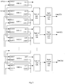
- Fig.2 shows a schematic diagram of a configuration of a first gate driving unit provided in an embodiment of the present disclosure.
- the first gate driving unit 12 comprises at least three GOA units, each of which comprises a signal input terminal INPUT, an output terminal OUT, a reset terminal RESET and an idle output terminal COUT.
- the signal input terminal INPUT of a first stage of GOA unit (S/R2-0 as shown in Fig.2 ) is input a first frame start signal STV1, and the reset terminal thereof is connected to the idle output terminal COUT of a third stage of GOA unit;
- the signal input terminal of a second stage of GOA unit (S/R1-1 as shown in Fig.2 ) is input a second frame start signal STV2;
- the reset terminal RESET of a 2n-th stage of GOA unit is connected to the idle output terminal COUT of a (2n-1)-th stage of GOA unit and the signal input terminal INPUT of a (2n+1)-th stage of GOA unit;
- the reset terminal RESET of the (2n+1)-th stage of GOA unit is connected to the idle output terminal COUT of a (2n+3)-th stage of GOA unit;
- the signal input terminal INPUT of a (2n+2)-th stage of GOA unit is connected to the idle output terminal COUT of a (2n-
- the logic or unit OR is capable of superimposing signals of the output terminal OUT of the 2n-th stage of GOA unit and the output terminal OUT of the (2n+1)-th stage of GOA unit in time domain and outputting them.
- Fig.3 shows a schematic diagram of a configuration of a second gate driving unit provided in an embodiment of the present disclosure.
- Fig.4 shows a schematic diagram of a configuration of a second gate driving unit provided in another embodiment of the present disclosure.
- the second gate driving unit can be implemented by any one of the two modes provided in Fig.3 or Fig.4 .
- the second gate driving unit 13 comprises at least three GOA units, each of which comprises a signal input terminal, an output terminal, a reset terminal and an idle output terminal;
- the signal input terminal of a first stage of GOA unit (S/R2-0) is input a third frame start signal, and the reset terminal thereof is connected to the idle output terminal of a third stage of GOA unit (S/R2-1);
- the signal input terminal of a second stage of GOA unit (S/R1-1) is input a fourth frame start signal;
- the reset terminal of a 2n-th stage of GOA unit is connected to the idle output terminal of a (2n-1)-th stage of GOA unit and the signal input terminal of a (2n+1)-th stage of GOA unit.
- the reset terminal of the (2n+1)-th stage of GOA unit is connected to the idle output terminal of a (2n+3)-th stage of GOA unit; the signal input terminal of a (2n+2)-th stage of GOA unit is connected to the idle output terminal of a (2n-2)-th stage of GOA unit.
- the output terminal of the 2n-th stage of GOA unit and the output terminal of the (2n+1)-th stage of GOA unit are connected to an input terminal of a logic or unit, an output terminal of the logic or unit is connected to an input terminal of a logic inverse unit, and an output terminal of the logic inverse unit outputs the second gate driving signal, where n is a positive integer.
- the logic inverse unit NG is capable of inversing a signal of the input terminal of the logic or unit OR 180° and then outputting the same.
- the second gate driving unit 13 comprises at least a pair of GOA units, each of which comprises a signal input terminal INPUT, an output terminal OUT, a reset terminal RESET and an idle output terminal COUT.
- the signal input terminal INPUT of a m-th stage of GOA unit is connected to the idle output terminal COUT of a (m-2)-th stage of GOA unit; the reset terminal RESET of the m-th stage of GOA unit is connected to the idle output terminal COUT of a (m+1)-th stage of GOA unit; the signal input terminal INPUT of a (m+1)-th stage of GOA unit is connected to the idle output terminal COUT of a (m-1)-th stage of GOA unit; and the reset terminal RESET of the (m+1)-th stage of GOA unit is connected to the idle output terminal COUT of a (m+3)-th stage of GOA unit.
- the reset terminal RESET of the first stage of GOA unit is connected to the idle output terminal COUT of the second stage of GOA unit; the reset terminal RESET of the second stage of GOA unit is connected to the idle output terminal COUT of a fourth stage of GOA unit.
- the signal input terminal INPUT of the first stage of GOA unit is input a fifth frame start signal
- the signal input terminal INPUT of the second stage of GOA unit is input a sixth frame start signal
- the output terminal of the m-th stage of GOA unit outputs the second gate driving signal to a pixel unit in a (m+1)/2-th row through the logic inverse unit, where m is an odd number.
- the logic inverse unit NG is capable of inversing a signal of the input terminal of the logic or unit OR 180° and then outputting the same.
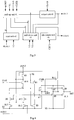
- Fig.5 shows a schematic diagram of a configuration of a GOA unit provided in an embodiment of the present disclosure.
- the GOA unit comprises: a pull-up unit 41, a pull-down unit 42, a reset unit 43, an idle output unit 44 and an output unit 45.
- the pull-up unit 41 is connected to the signal input terminal INPUT, a first level terminal V1, a first clock signal terminal CLKA, a second clock signal terminal CLKB, first node a, second node b, third node c and fourth node d.
- the pull-up unit 41 is configured to make a voltage of the first node a consistent with the signal input terminal INPUT, make a voltage of the second node b consistent with the signal input terminal INPUT or make the voltage of the second node b consistent with a voltage of the fourth node d, make a voltage of the third node c consistent with a voltage of the first level terminal V1, and make the voltage of the fourth node d consistent with a voltage of the first clock signal terminal CLKA under the control of signals of the signal input terminal INPUT, the first level terminal V1, the first clock signal terminal CLKA and the second clock signal terminal CLKB.
- the pull-down unit 42 is connected to a second level terminal V2, a third level terminal V3, the idle output terminal COUT, the output terminal OUT, the first node a, the second node b, the third node c and the fourth node d.
- the pull-down unit 42 is configured to make the voltage of the third node c consistent with the second level terminal V2 under the control of a signal of the first node a, make voltages of the first node a and the second node b consistent with the second level terminal uniform V2 under the control of a signal of the third node c, make a voltage of the output terminal OUT consistent with the second level terminal V2 under the control of the signal of the third node c, make a voltage of the output terminal OUT consistent with the third level terminal V3 under the control of the signal of the third node c, and make a voltage of the fourth node d consistent with the third level terminal V3 under the control of the signal of the third node c.
- the reset unit 43 is connected to the reset terminal RESET, the second level terminal V2, the second node b, and is connected to the first node a through the pull-down unit 42; and is configured to make the voltages of the first node a and the second node b consistent with the second level terminal V2 under the control of a signal of the reset terminal RESET.
- the idle output terminal 44 is connected to the second clock signal terminal CLKB and the idle output terminal COUT, and is connected to the first node a through the pull-down unit 42; and is configured to output a signal of the second clock signal terminal CLKB at the idle output terminal COUT under the control of the first node a.
- the output unit 45 is connected to the first node a, the second clock signal terminal CLKB and the output terminal OUT.
- the output unit 45 is configured to output the signal of the second clock signal terminal CLKB at the output terminal OUT under the control of the first node a.
- Fig.6 shows a schematic diagram of a configuration of a GOA unit provided in another embodiment of the present disclosure.
- the idle output unit comprises: a first transistor M1, whose gate is connected to the first node a, source is connected to the second clock signal terminal CLKB, and drain is connected to the idle output terminal COUT.
- the pull-up unit comprises: a fourth transistor M4, a sixth transistor M6, a seventh transistor M7, an eleventh transistor M11, and a fourteenth transistor M14.
- a gate and a source of the fourth transistor M4 are connected to the first level terminal V1, and a drain thereof is connected to the third node c.
- a gate and a source of the sixth transistor M6 are connected to the signal input terminal INPUT, and a drain thereof is connected to the second node b.
- a gate of the seventh transistor M7 is connected to the first node a, a source thereof is connected to the second clock signal terminal CLKB, and a drain thereof is connected to the fourth node d.
- a gate of the eleventh transistor M11 is connected to the idle output terminal COUT, a source thereof is connected to the second node b, and a drain thereof is connected to the fourth node d.
- a gate of the fourteenth transistor M14 is connected to the first clock signal terminal CLKA, a source thereof is connected to the second node b, and a drain thereof is connected to the first node a.
- the pull-down unit comprises: a second transistor M2, a third transistor M3, a fifth transistor M5, an eight transistor M8, a tenth transistor M10 and a thirteenth transistor M13.
- a gate of the second transistor M2 is connected to the third node c, a source thereof is connected to the idle output terminal COUT, and a drain thereof is connected to the second level terminal V2.
- a gate of the third transistor M3 is connected to the first node a, a source thereof is connected to the third node c, and a drain thereof is connected to the second level terminal V2.
- a gate of the fifth transistor M5 is connected to the third node c, a source thereof is connected to the first node a, and drain thereof is connected to the second node b.
- a gate of the eighth transistor M8 is connected to the third node c, a source thereof is connected to the fourth node d, and a drain thereof is connected to the third level terminal V3.
- a gate of the tenth transistor M10 is connected to the third node c, a source thereof is connected to the output terminal OUT, and a drain thereof is connected to the third level terminal V3.
- a gate of the thirteenth transistor M13 is connected to the third node c, a source thereof is connected to the second node b, and a drain thereof is connected to the second level terminal V2.
- the reset unit comprises: a twelfth transistor M12 and a fifteenth transistor M15.
- a gate of the twelfth transistor M12 is connected to the reset terminal RESET, a source thereof is connected to the first node a, and a drain thereof is connected to the second node b.
- a gate of the fifteenth transistor M15 is connected to the reset terminal RESET, a source thereof is connected to the second node b, and a drain thereof is connected to the second level terminal V2.
- the output unit comprises a ninth transistor M9, whose gate is connected to the first node a, source is connected to the second clock signal terminal CLKB, and drain is connected to the output terminal OUT.
- the first frame start signal is a single pulse signal
- the second frame start signal is a multi-pulse signal.
- the second frame start signal is a single pulse signal, and a pulse width of the second frame start signal comprises at least two clock cycles of a clock signal input to the first gate driving unit.
- the third frame start signal is a single pulse signal
- the fourth frame start signal is a multi-pulse signal.
- the fourth frame start signal is a single pulse signal, and a pulse width of the fourth frame start signal comprises at least two clock cycles of a clock signal input to the second gate driving unit.
- the fifth frame start signal is a multi-pulse signal
- the sixth frame start signal is a single pulse signal.
- the fifth frame start signal is a single pulse signal, and a pulse width of the fifth frame start signal comprises at least two clock cycles of a clock signal input to the first gate driving unit.
- the pixel unit 11 applied in the embodiment of the present disclosure can be any kind of pixel unit having the Vth compensating function, and the pixel unit 11 controls its operation timing through at least two gate driving signals.
- the specific circuit structure of the pixel unit 11 is not provided herein.
- the respective transistors in the GOA unit can be N type switching transistors or P type switching transistors.
- the description below takes the N type switching transistors as an example.
- the signal of the first level terminal V1 is a high level VGH
- the signal of the second level terminal V2 is a first low level VGL1
- the signal of the third level terminal V3 is a second low level VGL2.
- the first clock signal terminal CLKA of the odd number stage of GOA units (such as S/R2-0, S/R2-1 in Fig.2 ) is input a first clock signal CLK1, the second clock signal terminal CLKB thereof is input a second clock signal CLK2, and the signal input terminal INPUT of the first stage of GOA unit is input a first frame start signal STV1; wherein CLK1 and CLK2 are a pair of clock signals having inverse phases, that is, CLK1 and CLK2 has a phase difference of 180°.
- CLK1 and CLK2 have the same duty ratio (for example, their duty ratio is 50%), have the same frequency, and have a phase difference of 180°.
- a clock signal input to the first clock signal terminal CLKA of one GOA unit of two adjacent odd number stage of GOA units has a phase inverse to a clock signal input to the first clock signal terminal CLKA of another GOA unit of the two adjacent odd number stage of GOA units (i.e., having a phase difference of 180°).
- the first clock signal terminal CLKA of the GOA unit S/R1-2x is input a third clock signal CLK3, the second clock signal terminal CLKB thereof is input a fourth clock signal CLK4, the first clock signal terminal CLKA of the GOA unit S/R1-(2x-1) is input a fifth clock signal CLK5, and the second clock signal terminal CLKB thereof is input a sixth clock signal CLK6;
- the signal input terminal INPUT of the second stage of GOA unit (S/R1-1) is input a second frame start signal STV2;
- CLK3 and CLK4 are a pair of clock signals having inverse phases, that is, CLK3 and CLK4 has a phase difference of 180°.
- CLK3 and CLK4 have the same duty ratio (for example, their duty ratio is 50%), have the same frequency, and have a phase difference of 180°.
- CLK5 and CLK6 are a pair of clock signals having inverse phases, that is, CLK5 and CLK6 has a phase difference of 180°.
- CLK5 and CLK6 have the same duty ratio (for example, their duty ratio is 50%), have the same frequency, and have a phase difference of 180°.
- CLK3 and CLK5 have a preset phase difference.
- CLK3 and CLK5 have a phase difference of 90° or 180°, or a pulse rising edge of CLK5 delays a quarter of cycle or a half of cycle than a pulse rising edge of CLK3.
- the frequency of CLK3 is different from that of CLK1, for example, the frequency of CLK3 is greater than that of CLK1, that is, the pulse width of CLK3 is smaller than that of CLK1; the frequency of CLK5 is greater than that of CLK1, that is, the pulse width of CLK5 is smaller than that of CLK1.
- the pulse width of CLK3 is 50% of the pulse width of CLK1; the pulse width of CLK5 is 50% of the pulse width of CLK1.
- the respective transistors in the pull-up unit 41 are in a turn-on state, and the respective transistors in the pull-down unit 42 is in a turn-off state; the respective transistors in the reset unit 43 is in the turn-off state, and the respective transistors in the output unit 45 and the idle output unit 44 arc in the turn-on state.
- the output terminal of the second stage of GOA unit (S/R1-1) outputs a multi-pulse signal.
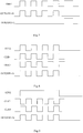
- Fig.8 there is provided a specific implementing mode of the multi-pulse signal.
- the second frame start signal STV2 is a multi-pulse signal.
- the pulse width of the second frame start signal STV2 is adjusted so that the pulse width of STV2 comprises at least two clock cycles of the clock signal CLK4 input to the first gate driving unit, that is, in the duration of one pulse width of STV2, CLK4 comprises four pulse signals.
- the output unit is capable of taking the signal of CLK4 as the output signal of the second stage of GOA unit (S/R1-1).
- the signal output from the output terminal of the second stage of GOA unit is the multi-pulse signal comprising four pulses.
- the input terminal INPUT of the 2n-th stage of GOA unit is also the multi-pulse signal (that is, a carry signal is also the multi-pulse signal). Therefore, the output terminal OUT of the 2n-th stage of GOA unit obtains the output of the multi-pulse signal too.
- the respective transistors of the pull-up unit 41 are in the turn-off state, and the respective transistors in the pull-down unit 42 are in the turn-on state.
- the respective transistors in the reset unit 43 are in the turn-on state, and the respective transistors in the output unit 45 and the idle output unit 44 are in the turn-off state.
- the OUT terminal of the output unit 45 docs not output, and the COUT terminal of the idle output terminal 44 does not output either.
- the respective transistors in the pull-up unit 41 are in the turn-on state, and the respective transistors in the pull-down unit 42 are in the turn-off state; the respective transistors in the reset unit 43 are in the turn-off state, and the respective transistors in the output unit 45 and the idle output unit 44 are in the turn-on state.
- the output terminal of the third stage of GOA unit (S/R2-1) outputs a single pulse signal, and thus the odd number stage of GOA unit sequence in the first gate driving unit 12 outputs the single pulse signal, which is a conventional mode, and thus is not described in detail in the embodiment of the present disclosure by combing with the timing diagrams of STV1, CLK1 and CLK2.
- the respective transistors in the pull-up unit 41 are in the turn-off state, and the respective transistors in the pull-down unit 42 are in the turn-on state; the respective transistors in the reset unit 43 are in the turn-on state, and the respective transistors in the output unit 45 and the idle output unit 44 are in the turn-off state.
- the OUT terminal of the output unit 45 does not output, and the COUT terminal of the idle output unit 44 does not output either.
- the output signal of the 2n-th stage of GOA unit and the output signal of the (2n+1)-th stage of GOA unit are superimposed by the logic or unit OR and output to obtain a gate driving signal Gate1 (n) of the pixel unit in the n-th row.
- the multi-pulse signal comprising four pulses, output from the output terminal of the second stage of GOA unit (S/R1-1) and the signal pulse signal output from the output terminal of the third stage of GOA unit (S/R2-1) are superimposed and output to obtain Gate1.
- Gate1 comprises one wide pulse signal and at least one narrow pulse signal with a fixed waveform.
- Gate1 comprising one wide pulse signal and four narrow pulse signals with a fixed waveform is just an example. The embodiment of the present disclose is not limited thereto, and there may be a combination of other forms.
- the first gate driving signal output by the first gate driving unit 12 as shown in Fig.2 is only inversed a phase of 180°, and then used as the second gate driving signal.
- the fifth frame start signal STV5 is similar to the third frame start signal STV3
- the sixth frame start signal STV6 is similar to the fourth frame start signal STV4. The specific principle is not further given herein.
- the first clock signal terminal CLKA of the odd number stage of GOA units is input a seventh clock signal CLK7
- the second clock signal terminal CLKB thereof is input an eighth clock signal CLK8
- the signal input terminal INPUT of the first state of GOA unit is input a fifth frame start signal STV5.
- CLK7 and CLK8 are a pair of clock signals having inverse phases, that is, CLK7 and CLK8 have a phase difference of 180°.
- CLK7 and CLK8 have the same duty ratio (for example, their duty ratio is 50%), have the same frequency, and have a phase difference of 180°.
- the clock signal input to the first clock signal terminal CLKA of one GOA unit of two adjacent odd number stage of GOA units has a phase inverse to the clock signal input to the first clock signal terminal CLKA of another GOA unit of the two adjacent odd number stage of GOA units (i.e., having a phase difference of 180°).
- the first clock signal terminal CLKA of the even number stage of GOA unit is input a ninth clock signal CLK9
- the second clock signal terminal CLKB thereof is input a tenth clock signal CLK10
- the input terminal INPUT of the second stage of GOA unit is input a sixth frame start signal STV6.
- CLK9 and CLK10 are a pair of clock signals having inverse phases, that is, CLK9 and CLK10 have a phase difference of 180°.
- CLK9 and CLK10 have the same duty ratio (for example, their duty ratio is 50%), have the same frequency, and have a phase difference of 180°.
- the clock signal input to the first clock signal terminal CLKA of one GOA unit of two adjacent even number stage of GOA units has a phase inverse to the clock signal input to the first clock signal terminal CLKA of another GOA unit of the two adjacent odd number stage of GOA units (i.e., having a phase difference of 180°).
- the respective transistors in the pull-up unit 41 are in a turn-on state, and the respective transistors in the pull-down unit 42 is in a turn-off state; the respective transistors in the reset unit 43 is in the turn-off state, and the respective transistors in the output unit 45 and the idle output unit 44 are in the turn-on state.
- the odd number stage of GOA units in the second gate driving unit 13 outputs a multi-pulse signal, which is used as a gate driving signal Gate2 of the pixel unit in the (m+1)/2-th row after a process of inversing a phase of 180°by the logic inverse unit NG, where m is an odd number.
- the respective transistors of the pull-up unit 41 arc in the turn-off state, and the respective transistors in the pull-down unit 42 are in the turn-on state.
- the respective transistors in the reset unit 43 are in the turn-on state, and the respective transistors in the output unit 45 and the idle output unit 44 are in the turn-off state. At this time, the OUT terminal of the output unit 45 does not output, and the COUT terminal of the idle output terminal 44 does not output either.
- the respective transistors in the pull-up unit 41 are in the turn-on state, and the respective transistors in the pull-down unit 42 are in the turn-off state; the respective transistors in the reset unit 43 are in the turn-off state, and the respective transistors in the output unit 45 and the idle output unit 44 are in the turn-on state.
- the even number stages of GOA units in the second gate driving unit 13 provide the reset signal input by the reset terminal RESET to the adjacent previous even number stage of GOA unit through the COUT terminal, and this reset signal can be a single pulse signal.
- the third state of GOA unit (S/R2-1) is similar to the odd number stage of GOA units in the first gate driving unit 12, and thus no further description is given herein.
- the respective transistors in the pull-up unit 41 are in the turn-off state, and the respective transistors in the pull-down unit 42 are in the turn-on state; the respective transistors in the reset unit 43 are in the turn-on state, and the respective transistors in the output unit 45 and the idle output unit 44 are in the turn-off state.
- the OUT terminal of the output unit 45 does not output
- the COUT terminal of the idle output unit 44 does not output either.
- timing states of the first gate driving signal generated by the first gate driving unit 12 and the second gate driving signal generated by the second gate driving unit 13 provided in Figs. 7, 8, 9 and 10 are just a possible implementation form.
- the first gate driving signal and the second gate driving signal in other timing states may be also generated to be output, to which no specific limitation is made.
- Fig. 11 is a flow schematic diagram of a driving method of a display circuit provided in an embodiment of the present disclosure. As shown in Fig.1 1 , there is provided a driving method of a display circuit in the embodiment of the present disclosure, comprising following steps:
- the first gate driving signal and the second gate driving signal are multi-pulse signals.
- the first gate driving signal is a pulse signal comprising at least two kinds of pulse width
- the second gate driving signal is a pulse signal comprising at least two kinds of pulse width.
- the first gate driving signal is input to the pixel unit through the first gate driving unit
- the second gate driving signal is input to the pixel unit through the second gate driving unit
- the pixel unit is controlled by the first gate driving signal and the second gate driving signal to perform threshold compensating and gray scale displaying simultaneously. Since threshold compensating and gray scale displaying of the pixel unit can be performed simultaneously under the control of signals of two gate driving units, the complexity in design of the display circuit can be reduced, which is advantageous for raising density of pixels of the display panel, so that resolution of the display panel is raised.
- a display apparatus comprising any one of the display circuits described above, wherein the display circuit comprises a pixel unit, a first gate driving unit and a second gate driving unit.
- the display apparatus can be a display device such as an electronic paper, a mobile phone, a TV set, a digital photo frame, etc.
Landscapes
- Engineering & Computer Science (AREA)
- Physics & Mathematics (AREA)
- Computer Hardware Design (AREA)
- General Physics & Mathematics (AREA)
- Theoretical Computer Science (AREA)
- Control Of Indicators Other Than Cathode Ray Tubes (AREA)
Claims (14)
- Anzeigeschaltung, umfassend eine Mehrzahl von in einer Matrix angeordneten Pixeleinheiten (11), eine erste Gate-Treibereinheit (12) und eine zweite Gate-Treibereinheit (13);
wobei die erste Gate-Treibereinheit (12) konfiguriert ist, ein erstes Gate-Ansteuerungssignal auszugeben zu einem ersten Eingang von jeder von der Mehrzahl von Pixeleinheiten (11);
wobei die zweite Gate-Treibereinheit (13) konfiguriert ist, ein zweites Gate-Ansteuerungssignal auszugeben zu einem zweiten Eingang von jeder von der Mehrzahl von Pixeleinheiten (11);
dadurch gekennzeichnet, dass die erste Gate-Treibereinheit (12) zumindest drei GOA-Stufeneinheiten umfasst, wobei jede der GOA-Stufeneinheiten einen Signaleingabeanschluss (INPUT), einen Ausgabeanschluss (OUT), einen Rücksetzanschluss (RESET) und einen zweiten Ausgabeanschluss (COUT) umfasst;
wobei der Signaleingabeanschluss (INPUT) der ersten GOA-Stufeneinheit (S/R2-0) geeignet ist, ein erstes Bildstartsignal (STV1) dafür eingegeben zu bekommen, und ein Rücksetzanschluss davon an den zweiten Ausgabeanschluss (COUT) der dritten GOA-Stufeneinheit (S/R2-1) angeschlossen ist;
wobei der Signaleingabeanschluss (INPUT) der zweiten GOA-Stufeneinheit (S/R1-1) geeignet ist, ein zweites Bildstartsignal (STV2) dafür eingegeben zu bekommen, und der Rücksetzanschluss (RESET) davon an den zweiten Ausgabeanschluss (COUT) der ersten GOA-Stufeneinheit angeschlossen ist; wobei
der zweite Ausgabeanschluss (COUT) der ersten GOA-Stufeneinheit (S/R2-0) an den Rücksetz-Anschluss (RESET) der zweiten GOA-Stufeneinheit (S/R1-1) und den Signaleingabeanschluss (INPUT) der dritten GOA-Stufeneinheit (S/R2-1) angeschlossen ist;
wobei der Ausgabeanschluss (OUT) der zweiten GOA-Stufeneinheit (S/R1-1) und der Ausgabeanschluss der dritten GOA-Stufeneinheit geeignet sind, das erste Gate-Ansteuerungssignal (Gate(1)) an eine Pixeleinheit in einer ersten Reihe durch eine Logik-ODER-Einheit auszugeben;
wobei der zweite Ausgabeanschluss (COUT) einer (2n+1)-ten GOA-Stufeneinheit (S/R2-1, S/R2-n) an den Rücksetzeingabeanschluss (RESET) der (2n-1)-ten GOA-Stufeneinheit (S/R2-0, S/R2-n-1), den Rücksetzeingabeanschluss der (2n+2)-ten GOA-Stufeneinheit (S/R1-2, S/R1-n+1) und den Signaleingabeanschluss (INPUT) der (2n+3)-ten GOA-Stufeneinheit (S/R2-2, S/R2-n+1) angeschlossen ist; und wobei der zweite Ausgabeanschluss (COUT) von der 2n-ten GOA-Stufeneinheit (S/R1-1, S/R1-n) an den Eingabeanschluss (INPUT) einer (2n+2)-ten GOA-Stufeneinheit (S/R1-2, S/R1-n+1) angeschlossen ist; und
wobei der Ausgabeanschluss der 2n-ten GOA-Stufeneinheit und der Ausgabeanschluss der (2n+1)-ten GOA-Stufeneinheit geeignet sind, das erste Gate-Ansteuerungssignal an eine Pixeleinheit in einer n-ten Reihe durch eine n-te Logik-ODER-Einheit auszugeben, wobei n eine positive Ganzzahl größer als oder gleich 2 ist. - Anzeigeschaltung gemäß Anspruch 1, wobei die zweite Gate-Treibereinheit (13) zumindest drei GOA-Stufeneinheiten umfasst,
von denen jede einen Signaleingabeanschluss, einen Ausgabeanschluss, einen Rücksetzanschluss und einen zweiten Ausgabeanschluss umfasst,
wobei der Signaleingabeanschluss der ersten GOA-Stufeneinheit geeignet ist, ein drittes Bildstartsignal (STV3) dafür eingegeben zu bekommen, und der Rücksetzanschluss davon an den zweiten Ausgabeanschluss einer dritten GOA-Stufeneinheit angeschlossen ist;
wobei der Signaleingabeanschluss der zweiten GOA-Stufeneinheit geeignet ist, ein viertes Bildstartsignal (STV4) dafür eingegeben zu bekommen, und der Rücksetzanschluss davon an den zweiten Ausgabeanschluss der ersten GOA-Stufeneinheit und den Signaleingabeanschluss der dritten GOA-Stufeneinheit angeschlossen ist;
wobei der zweite Ausgabeanschluss von einer (2n+1)-ten GOA-Stufeneinheit an den Rücksetzeingabeanschluss der (2n-1)-ten GOA-Stufeneinheit, den Rücksetzeingabeanschluss der (2n+2)-ten GOA-Stufeneinheit und den Signaleingabeanschluss der (2n+3)-ten GOA-Stufeneinheit angeschlossen ist; und
wobei der zweite Ausgabeanschluss von einer 2n-ten GOA-Stufeneinheit an den Eingabeanschluss einer (2n+2)-ten GOA-Stufeneinheit angeschlossen ist;
wobei der Ausgabeanschluss der 2n-ten GOA-Stufeneinheit und der Ausgabeanschluss der (2n+1)-ten GOA-Stufeneinheit geeignet sind, an betreffende Eingabeanschlüsse einer Logik-ODER-Einheit angeschlossen zu werden,
ein Ausgabeanschluss der Logik-ODER-Einheit geeignet ist, an einen Eingabeanschluss einer Logik-Umkehr-Einheit (NG) angeschlossen zu werden, und ein Ausgabeanschluss der Logik-Umkehr-Einheit geeignet ist, das zweite Gate-Ansteuerungssignal auszugeben, wobei n eine positive Ganzzahl ist. - Anzeigeschaltung gemäß Anspruch 1, wobei die zweite Gate-Treibereinheit (13) zumindest ein Paar GOA-Stufeneinheiten umfasst, von denen jede einen Signaleingabeanschluss, einen Ausgabeanschluss, einen Rücksetzanschluss und einen zweiten Ausgabeanschluss umfasst,
wobei, ausgenommen für die erste Stufe der GOA-Einheit und die zweite Stufe der GOA-Einheit, ein Signaleingabeanschluss einer m-ten GOA-Stufeneinheit an den zweiten Ausgabeanschluss einer (m-2)-ten Stufe einer GOA-Stufeneinheit angeschlossen ist; wobei ein Rücksetzanschluss der m-ten GOA-Stufeneinheit an den zweiten Ausgabeanschluss einer (m+1)-ten GOA-Stufeneinheit angeschlossen ist;
wobei ein Signaleingabeanschluss einer (m+1)-ten GOA-Stufeneinheit an den zweiten Ausgabeanschluss einer (m-1)-ten GOA-Stufeneinheit angeschlossen ist; und wobei ein Rücksetzanschluss der (m+1)-ten GOA-Stufeneinheit an den zweiten Ausgabeanschluss einer (m+3)-ten GOA-Stufeneinheit angeschlossen ist;
wobei ein Rücksetzanschluss der ersten GOA-Stufeneinheit an den zweiten Ausgabeanschluss der zweiten GOA-Stufeneinheit angeschlossen ist; wobei ein Rücksetzanschluss der zweiten GOA-Stufeneinheit an den zweiten Ausgabeanschluss einer vierten GOA-Stufeneinheit angeschlossen ist;
wobei ein Signaleingabeanschluss der ersten GOA-Stufeneinheit geeignet ist, ein fünftes Bildstartsignal dafür eingegeben zu bekommen, und wobei ein Signaleingabeanschluss der zweiten GOA-Stufeneinheit geeignet ist, ein sechstes Bildstartsignal dafür eingegeben zu bekommen; und
wobei ein Ausgabeanschluss der m-ten GOA-Stufeneinheit das zweite Gate-Ansteuerungssignal an eine Pixeleinheit in einer (m+1)2-ten Reihe durch die Logik-Umkehr-Einheit ausgibt, wobei m eine ungerade Zahl ist. - Anzeigeschaltung gemäß einem der Ansprüche 1- 3, wobei eine GOA-Stufeneinheit umfasst: eine Pull-Up-Einheit (41), eine Pull-Down-Einheit (42), eine Rücksetzeinheit (43), eine zweite Ausgabeeinheit (44) und eine Ausgabeeinheit (45);
wobei die Pull-Up-Einheit an den Signaleingabeanschluss, einen ersten Pegelanschluss (V1), einen ersten Taktsignalanschluss (CLKA), einen zweiten Taktsignalanschluss (CLKB), einen ersten Knoten (a), einen zweiten Knoten (b), einen dritten Knoten (c) und einen vierten Knoten (d) angeschlossen ist, und konfiguriert ist, eine Spannung des ersten Knotens gleich zu einer Spannung an dem Signaleingabeanschluss zu machen, eine Spannung des zweiten Knotens gleich zu der Spannung an dem Signaleingabeanschluss zu machen oder die Spannung des zweiten Knotens gleich zu einer Spannung des vierten Knotens zu machen, eine Spannung des dritten Knotens gleich zu einer Spannung des ersten Pegelanschlusses zu machen, und die Spannung des vierten Knotens gleich zu einer Spannung des ersten Taktsignalanschlusses zu machen unter der Steuerung von Signalen des Signaleingabeanschlusses, des ersten Pegelanschlusses, des ersten Taktsignalanschlusses und des zweiten Taktsignalanschlusses;
wobei die Pull-Down-Einheit an den zweiten Pegelanschluss (V2), einen dritten Pegelanschluss (V3), einen Leer-Ausgabeanschluss, den Ausgabeanschluss, einen ersten Knoten, einen zweiten Knoten, einen dritten Knoten und einen vierten Knoten angeschlossen ist, und konfiguriert ist, eine Spannung des dritten Knotens gleich zu einer Spannung an dem zweiten Pegelanschluss zu machen unter der Steuerung eines Signals des ersten Knotens, Spannungen des ersten Knotens gleich zu einer Spannung an dem zweiten Knoten und dem zweiten Pegelanschluss zu machen unter der Steuerung eines Signals des dritten Knotens, eine Spannung des Ausgabeanschlusses gleich zu der Spannung an dem zweiten Pegelanschluss zu machen unter der Steuerung des Signals des dritten Knotens, eine Spannung des Ausgabeanschlusses gleich zu einer Spannung an dem dritten Pegelanschluss zu machen unter der Steuerung des Signals des dritten Knotens, und eine Spannung des vierten Knotens gleich zu einer Spannung an dem dritten Pegelanschluss zu machen unter der Steuerung des Signals des dritten Knotens;
wobei die Rücksetzeinheit an den Rücksetzanschluss, den zweiten Pegelanschluss, den ersten Knoten und den zweiten Knoten angeschlossen ist und konfiguriert ist, die Spannungen des ersten Knotens und des zweiten Knotens gleich zu einer Spannung an dem zweiten Pegelanschluss zu machen unter der Steuerung eines Signals des Rücksetzanschlusses;
wobei die zweite Ausgabeeinheit an den ersten Knoten, den zweiten Taktsignalanschluss und den zweiten Ausgabeanschluss angeschlossen ist und konfiguriert ist, ein Signal des zweiten Taktsignalanschlusses an den Leerausgabeanschluss unter der Steuerung des ersten Knotens auszugeben; und
wobei die Ausgabeeinheit an den ersten Knoten, den zweiten Taktsignalanschluss und den Ausgabeanschluss angeschlossen ist und konfiguriert ist, das Signal des zweiten Taktsignalanschlusses an den Ausgabeanschluss auszugeben unter der Steuerung des ersten Knotens. - Anzeigeschaltung gemäß Anspruch 4, wobei die zweite Ausgabeeinheit umfasst:
einen Leerausgabetransistor (M1), dessen Gate an den ersten Knoten angeschlossen ist, dessen Source an den zweiten Taktsignalanschluss angeschlossen ist und dessen Drain an den zweiten Ausgabeanschluss angeschlossen ist. - Anzeigeschaltung gemäß Anspruch 4, wobei die Pull-Up-Einheit umfasst: einen ersten Pull-Up-Transistor (M4), einen zweiten Pull-Up-Transistor (M6), einen dritten Pull-Up-Transistor (M7), einen vierten Pull-Up-Transistor (M11) und einen fünften Pull-Up-Transistor (M14);
wobei ein Gate und eine Source des ersten Pull-Up-Transistors (M4) an den ersten Pegelanschluss (V1) angeschlossen sind und ein Drain davon an den dritten Knoten (c) angeschlossen ist;
wobei ein Gate und eine Source des zweiten Pull-Up-Transistors (M6) an den Signaleingabeanschluss angeschlossen sind und ein Drain davon an den zweiten Knoten (b) angeschlossen ist;
wobei ein Gate des dritten Pull-Up-Transistors (M7) an den ersten Knoten (a) angeschlossen ist, eine Source davon an den zweiten Taktsignalanschluss (CLKB) angeschlossen ist und ein Drain davon an den vierten Knoten (d) angeschlossen ist;
wobei ein Gate des vierten Pull-Up-Transistors (M11) an den zweiten Ausgabeanschluss angeschlossen ist, eine Source davon an den zweiten Knoten (b) angeschlossen ist und ein Drain davon an den vierten Knoten (d) angeschlossen ist;
und wobei ein Gate des fünften Pull-Up-Transistors (M14) an den ersten Taktsignalanschluss (CLKA) angeschlossen ist, eine Source davon an den zweiten Knoten (b) angeschlossen ist und ein Drain davon an den ersten Knoten (a) angeschlossen ist. - Anzeigeschaltung gemäß Anspruch 4, wobei die Pull-Down-Einheit umfasst:
einen ersten Pull-Down-Transistor (M2), einen zweiten Pull-Down-Transistor (M3), einen dritten Pull-Down-Transistor (M5), einen vierten Pull-Down-Transistor (M8), einen fünften Pull-Down-Transistor (M10) und einen sechsten Pull-Down-Transistor (M13);wobei ein Gate des ersten Pull-Down-Transistors (M2) an den dritten Knoten (c) angeschlossen ist, eine Source davon an den Leer-Ausgabeanschluss angeschlossen ist und ein Drain davon an den zweiten Pegelanschluss (V2) angeschlossen ist;wobei ein Gate des zweiten Pull-Down-Transistors (M3) an den ersten Knoten (a) angeschlossen ist, eine Source davon an den dritten Knoten (c) angeschlossen ist und ein Drain davon an den zweiten Pegelanschluss (V2) angeschlossen ist;wobei ein Gate des dritten Pull-Down-Transistors (M5) an den dritten Knoten (c) angeschlossen ist, eine Source davon an den ersten Knoten (a) angeschlossen ist und ein Drain davon an den zweiten Knoten (b) angeschlossen ist;wobei ein Gate des vierten Pull-Down-Transistors (M8) an den dritten Knoten (c) angeschlossen ist, eine Source davon an den vierten Knoten (d) angeschlossen ist und ein Drain davon an den dritten Pegelanschluss (V3) angeschlossen ist;wobei ein Gate des fünften Pull-Down-Transistors (M10) an den dritten Knoten (c) angeschlossen ist, eine Source davon an den Ausgabeanschluss angeschlossen ist und ein Drain davon an den dritten Pegelanschluss (V3) angeschlossen ist; undwobei ein Gate des sechsten Pull-Down-Transistors (M13) an den dritten Knoten (c) angeschlossen ist, eine Source davon an den zweiten Knoten (b) angeschlossen ist und ein Drain davon an den zweiten Pegelanschluss (V2) angeschlossen ist. - Anzeigeschaltung gemäß Anspruch 4, wobei die Rücksetzeinheit umfasst: einen ersten Rücksetztransistor (M12) und einen zweiten Rücksetztransistor (M15), wobei
ein Gate des ersten Rücksetztransistors (M12) an den Rücksetzanschluss angeschlossen ist, eine Source davon an den ersten Knoten (a) angeschlossen ist und ein Drain davon an den zweiten Knoten (b) angeschlossen ist; und
wobei ein Gate des zweiten Rücksetztransistors (M15) an den Rücksetzanschluss angeschlossen ist, eine Source davon an den zweiten Knoten (b) angeschlossen ist und ein Drain davon an den zweiten Pegelanschluss (V2) angeschlossen ist. - Anzeigeschaltung gemäß Anspruch 4, wobei die Ausgabeeinheit einen Ausgabetransistor (M9) umfasst, dessen Gate an den ersten Knoten (a) angeschlossen ist, dessen Source an den zweiten Taktsignalanschluss (CKLB) angeschlossen ist und dessen Drain an den Ausgabeanschluss angeschlossen ist.
- Anzeigeschaltung gemäß Anspruch 1, wobei das erste Bildstartsignal ein Einzelimpulssignal ist und das zweite Bildstartsignal ein Multiimpulssignal ist;
oder das zweite Bildstartsignal ist ein Einzelimpulssignal, und eine Impulsbreite des zweiten Bildstartsignals umfasst zumindest zwei Taktzyklen eines der ersten Gate-Treibereinheit eingegebenen Taktsignals. - Anzeigeschaltung gemäß Anspruch 2, wobei das dritte Bildstartsignal ein Einzelimpulssignal ist und das vierte Bildstartsignal ein Multiimpulssignal ist;
oder das vierte Bildstartsignal ist ein Einzelimpulssignal, und eine Impulsbreite des vierten Bildstartsignals umfasst zumindest zwei Taktzyklen eines der zweiten Gate-Treibereinheit eingegebenen Taktsignals. - Anzeigeschaltung gemäß Anspruch 3, wobei das fünfte Bildstartsignal ein Multiimpulssignal ist und das sechste Bildstartsignal ein Einzelimpulssignal ist;
oder das fünfte Bildstartsignal ist ein Einzelimpulssignal, und eine Impulsbreite des fünften Bildstartsignals umfasst zumindest zwei Taktzyklen eines der ersten Gate-Treibereinheit eingegebenen Taktsignals. - Ansteuerungsverfahren, angewendet auf die Anzeigeschaltung gemäß einem der Ansprüche 1 - 12, umfassend folgende Schritte:Eingeben des ersten Gate-Ansteuerungssignals an jede von der Mehrzahl von Pixeleinheiten mittels der ersten Gate-Treibereinheit;Eingeben des zweiten Gate-Ansteuerungssignals an jede von der Mehrzahl von Pixeleinheiten mittels der zweiten Gate-Treibereinheit.
- Anzeigevorrichtung, umfassend die Anzeigeschaltung gemäß einem der Ansprüche 1 - 12.
Applications Claiming Priority (2)
| Application Number | Priority Date | Filing Date | Title |
|---|---|---|---|
| CN201410554799.9A CN104282269B (zh) | 2014-10-17 | 2014-10-17 | 一种显示电路及其驱动方法和显示装置 |
| PCT/CN2015/077376 WO2016058351A1 (zh) | 2014-10-17 | 2015-04-24 | 显示电路及其驱动方法和显示装置 |
Publications (3)
| Publication Number | Publication Date |
|---|---|
| EP3208791A1 EP3208791A1 (de) | 2017-08-23 |
| EP3208791A4 EP3208791A4 (de) | 2018-04-11 |
| EP3208791B1 true EP3208791B1 (de) | 2020-08-19 |
Family
ID=52257100
Family Applications (1)
| Application Number | Title | Priority Date | Filing Date |
|---|---|---|---|
| EP15775602.4A Active EP3208791B1 (de) | 2014-10-17 | 2015-04-24 | Anzeigeschaltung und ansteuerungsverfahren dafür sowie anzeigevorrichtung |
Country Status (4)
| Country | Link |
|---|---|
| US (1) | US9997136B2 (de) |
| EP (1) | EP3208791B1 (de) |
| CN (1) | CN104282269B (de) |
| WO (1) | WO2016058351A1 (de) |
Families Citing this family (15)
| Publication number | Priority date | Publication date | Assignee | Title |
|---|---|---|---|---|
| CN104282269B (zh) * | 2014-10-17 | 2016-11-09 | 京东方科技集团股份有限公司 | 一种显示电路及其驱动方法和显示装置 |
| CN104282270B (zh) | 2014-10-17 | 2017-01-18 | 京东方科技集团股份有限公司 | 栅极驱动电路、显示电路及驱动方法和显示装置 |
| CN104537977B (zh) | 2015-01-20 | 2017-08-11 | 京东方科技集团股份有限公司 | 一种goa单元及驱动方法、goa电路和显示装置 |
| CN104992686A (zh) | 2015-07-21 | 2015-10-21 | 京东方科技集团股份有限公司 | 一种显示面板及其驱动方法、驱动装置 |
| CN105427811B (zh) * | 2015-12-24 | 2018-08-14 | 上海天马有机发光显示技术有限公司 | 一种有机发光显示面板及电子设备 |
| CN105448227B (zh) * | 2016-01-12 | 2017-11-17 | 京东方科技集团股份有限公司 | 一种栅极驱动电路和显示装置 |
| CN105448226B (zh) * | 2016-01-12 | 2018-03-16 | 京东方科技集团股份有限公司 | 一种栅极驱动电路和显示装置 |
| JP6668193B2 (ja) * | 2016-07-29 | 2020-03-18 | 株式会社ジャパンディスプレイ | センサ及び表示装置 |
| CN106328054B (zh) * | 2016-10-24 | 2018-07-10 | 武汉华星光电技术有限公司 | Oled显示goa扫描驱动电路 |
| CN108122534B (zh) | 2016-11-29 | 2019-03-26 | 昆山国显光电有限公司 | 一种驱动控制电路及其驱动方法、显示装置 |
| KR102423863B1 (ko) * | 2017-08-04 | 2022-07-21 | 엘지디스플레이 주식회사 | 게이트 구동부 및 이를 구비한 평판 표시 장치 |
| KR102458156B1 (ko) * | 2017-08-31 | 2022-10-21 | 엘지디스플레이 주식회사 | 표시 장치 |
| CN108877638B (zh) * | 2018-09-21 | 2021-06-04 | 重庆惠科金渝光电科技有限公司 | 驱动电路、升压芯片及显示装置 |
| CN110060639B (zh) * | 2019-04-24 | 2021-07-06 | 深圳市华星光电半导体显示技术有限公司 | 阵列基板 |
| CN114882831A (zh) | 2022-05-13 | 2022-08-09 | 武汉华星光电半导体显示技术有限公司 | 一种显示面板的显示控制方法、显示模组及显示装置 |
Family Cites Families (39)
| Publication number | Priority date | Publication date | Assignee | Title |
|---|---|---|---|---|
| JP3810725B2 (ja) * | 2001-09-21 | 2006-08-16 | 株式会社半導体エネルギー研究所 | 発光装置及び電子機器 |
| KR100853720B1 (ko) * | 2002-06-15 | 2008-08-25 | 삼성전자주식회사 | 비정질-실리콘 박막 트랜지스터 게이트 구동 쉬프트레지스터 및 이를 가지는 액정 표시 장치 |
| GB0320503D0 (en) | 2003-09-02 | 2003-10-01 | Koninkl Philips Electronics Nv | Active maxtrix display devices |
| KR100515305B1 (ko) * | 2003-10-29 | 2005-09-15 | 삼성에스디아이 주식회사 | 발광 표시 장치 및 그 표시 패널과 구동 방법 |
| KR101032945B1 (ko) | 2004-03-12 | 2011-05-09 | 삼성전자주식회사 | 시프트 레지스터 및 이를 포함하는 표시 장치 |
| KR101080351B1 (ko) * | 2004-06-22 | 2011-11-04 | 삼성전자주식회사 | 표시 장치 및 그 구동 방법 |
| KR100592645B1 (ko) * | 2004-11-08 | 2006-06-26 | 삼성에스디아이 주식회사 | 화소 및 이를 이용한 발광 표시장치와 그의 구동방법 |
| JP5081374B2 (ja) | 2005-01-17 | 2012-11-28 | 株式会社ジャパンディスプレイイースト | 画像表示装置 |
| JP2006251515A (ja) * | 2005-03-11 | 2006-09-21 | Fuji Photo Film Co Ltd | 表示装置 |
| KR100667075B1 (ko) * | 2005-07-22 | 2007-01-10 | 삼성에스디아이 주식회사 | 주사 구동부 및 이를 포함하는 유기 전계발광 표시장치 |
| KR100552451B1 (ko) | 2005-07-27 | 2006-02-21 | 실리콘 디스플레이 (주) | 문턱전압이 보상되는 요철 검출장치 및 그 방법 |
| KR101209055B1 (ko) | 2005-09-30 | 2012-12-06 | 삼성디스플레이 주식회사 | 표시 장치 및 그 구동 방법 |
| JP4151714B2 (ja) * | 2006-07-19 | 2008-09-17 | ソニー株式会社 | 表示装置及びその駆動方法 |
| KR20080010986A (ko) | 2006-07-28 | 2008-01-31 | 삼성전자주식회사 | 구동 장치 및 이를 포함하는 액정 표시 장치 |
| TWI831616B (zh) * | 2006-09-29 | 2024-02-01 | 日商半導體能源研究所股份有限公司 | 半導體裝置 |
| CN101192381B (zh) * | 2006-11-29 | 2010-12-22 | 群康科技(深圳)有限公司 | 液晶显示器及其驱动电路和驱动方法 |
| CN100582880C (zh) * | 2006-12-01 | 2010-01-20 | 群康科技(深圳)有限公司 | 液晶显示器及其驱动电路 |
| JP2008241782A (ja) * | 2007-03-26 | 2008-10-09 | Sony Corp | 表示装置及びその駆動方法と電子機器 |
| KR101307414B1 (ko) | 2007-04-27 | 2013-09-12 | 삼성디스플레이 주식회사 | 게이트 구동 회로 및 이를 포함하는 액정 표시 장치 |
| JP5309475B2 (ja) * | 2007-06-05 | 2013-10-09 | ソニー株式会社 | 表示パネル駆動方法、表示装置、表示パネル駆動装置及び電子機器 |
| CN101408684B (zh) * | 2007-10-12 | 2010-08-25 | 群康科技(深圳)有限公司 | 液晶显示装置及其驱动方法 |
| JP5151585B2 (ja) * | 2008-03-18 | 2013-02-27 | ソニー株式会社 | 半導体デバイス、表示パネル及び電子機器 |
| TWI334124B (en) * | 2008-08-28 | 2010-12-01 | Au Optronics Corp | Display drive circuit for flat panel display and driving method for gate lines |
| US8599222B2 (en) | 2008-09-04 | 2013-12-03 | Seiko Epson Corporation | Method of driving pixel circuit, light emitting device, and electronic apparatus |
| JP2010191935A (ja) | 2009-01-26 | 2010-09-02 | Toshiba Tec Corp | 注文受付装置およびプログラム |
| KR101210029B1 (ko) * | 2010-05-17 | 2012-12-07 | 삼성디스플레이 주식회사 | 유기전계발광 표시장치 |
| CN201681587U (zh) * | 2010-05-24 | 2010-12-22 | 北京京东方光电科技有限公司 | 双面液晶显示设备 |
| KR101781137B1 (ko) * | 2010-07-20 | 2017-09-25 | 삼성디스플레이 주식회사 | 유기전계발광 표시장치 |
| KR101536129B1 (ko) | 2011-10-04 | 2015-07-14 | 엘지디스플레이 주식회사 | 유기발광 표시장치 |
| CN102654968B (zh) * | 2011-11-25 | 2014-12-10 | 京东方科技集团股份有限公司 | 移位寄存器、栅极驱动器及显示装置 |
| KR101350592B1 (ko) | 2011-12-12 | 2014-01-16 | 엘지디스플레이 주식회사 | 유기발광 표시장치 |
| KR101528148B1 (ko) | 2012-07-19 | 2015-06-12 | 엘지디스플레이 주식회사 | 화소 전류 측정을 위한 유기 발광 다이오드 표시 장치 및 그의 화소 전류 측정 방법 |
| KR102007814B1 (ko) * | 2012-12-14 | 2019-08-07 | 엘지디스플레이 주식회사 | 표시장치와 그 게이트 구동회로의 제어 방법 |
| CN103941439B (zh) | 2013-06-28 | 2016-09-28 | 上海中航光电子有限公司 | 一种补偿馈通电压驱动电路及阵列基板 |
| US9171516B2 (en) * | 2013-07-03 | 2015-10-27 | Shenzhen China Star Optoelectronics Technology Co., Ltd | Gate driver on array circuit |
| CN103345941B (zh) | 2013-07-03 | 2016-12-28 | 京东方科技集团股份有限公司 | 移位寄存器单元及驱动方法、移位寄存器电路及显示装置 |
| KR102211692B1 (ko) * | 2014-09-03 | 2021-02-04 | 삼성디스플레이 주식회사 | 유기 발광 다이오드 표시 장치 |
| CN104282270B (zh) * | 2014-10-17 | 2017-01-18 | 京东方科技集团股份有限公司 | 栅极驱动电路、显示电路及驱动方法和显示装置 |
| CN104282269B (zh) | 2014-10-17 | 2016-11-09 | 京东方科技集团股份有限公司 | 一种显示电路及其驱动方法和显示装置 |
-
2014
- 2014-10-17 CN CN201410554799.9A patent/CN104282269B/zh active Active
-
2015
- 2015-04-24 WO PCT/CN2015/077376 patent/WO2016058351A1/zh not_active Ceased
- 2015-04-24 EP EP15775602.4A patent/EP3208791B1/de active Active
- 2015-04-24 US US14/787,893 patent/US9997136B2/en active Active
Non-Patent Citations (1)
| Title |
|---|
| None * |
Also Published As
| Publication number | Publication date |
|---|---|
| CN104282269A (zh) | 2015-01-14 |
| CN104282269B (zh) | 2016-11-09 |
| EP3208791A4 (de) | 2018-04-11 |
| US9997136B2 (en) | 2018-06-12 |
| EP3208791A1 (de) | 2017-08-23 |
| US20160189677A1 (en) | 2016-06-30 |
| WO2016058351A1 (zh) | 2016-04-21 |
Similar Documents
| Publication | Publication Date | Title |
|---|---|---|
| EP3208791B1 (de) | Anzeigeschaltung und ansteuerungsverfahren dafür sowie anzeigevorrichtung | |
| EP3208792B1 (de) | Gate-treiberschaltung, anzeigeschaltung, ansteuerungsverfahren und anzeigevorrichtung | |
| CN110164352B (zh) | 移位寄存器电路及其驱动方法、栅极驱动电路和显示面板 | |
| US9791968B2 (en) | Shift register, its driving method, gate driver circuit and display device | |
| US10930360B2 (en) | Shift register, driving method thereof, gate driving circuit, and display device | |
| EP3846156B1 (de) | Schieberegistereinheit, ansteuerungsverfahren dafür, gate-treiber und anzeigevorrichtung | |
| KR101718272B1 (ko) | 게이트 구동기, 디스플레이 장치 및 게이트 구동 방법 | |
| US10950322B2 (en) | Shift register unit circuit, method of driving the same, gate drive circuit, and display apparatus | |
| US8941629B2 (en) | Scan driver and organic light emitting display device using the same | |
| US11355068B2 (en) | Shift register unit, gate drive circuit and drive method | |
| US10878757B2 (en) | Shift register and time-sharing controlling method thereof, display panel and display apparatus | |
| CN111583880B (zh) | 移位寄存器单元电路及驱动方法、栅极驱动器和显示装置 | |
| CN103730089A (zh) | 栅极驱动电路、方法、阵列基板行驱动电路和显示装置 | |
| JP2011248944A (ja) | 走査線駆動回路 | |
| US11393402B2 (en) | OR logic operation circuit and driving method, shift register unit, gate drive circuit, and display device | |
| US11081031B2 (en) | Gate control unit, driving method thereof, gate driver on array and display apparatus | |
| US20160372041A1 (en) | Scan Driving Circuit and Display Device | |
| US20160293081A1 (en) | Display With Driver Circuitry Having Intraframe Pause Capabilities | |
| JP2020534552A (ja) | アレイ基板行駆動回路、amoled表示パネルの画素回路、amoled表示パネル及びamoled表示パネルの画素回路の駆動方法 | |
| US9805638B2 (en) | Shift register, array substrate and display apparatus | |
| US10770002B2 (en) | Shift register circuit, driving method thereof, gate driver and display panel | |
| US11158224B2 (en) | Start signal generation circuit, driving method and display device |
Legal Events
| Date | Code | Title | Description |
|---|---|---|---|
| STAA | Information on the status of an ep patent application or granted ep patent |
Free format text: STATUS: THE INTERNATIONAL PUBLICATION HAS BEEN MADE |
|
| PUAI | Public reference made under article 153(3) epc to a published international application that has entered the european phase |
Free format text: ORIGINAL CODE: 0009012 |
|
| STAA | Information on the status of an ep patent application or granted ep patent |
Free format text: STATUS: REQUEST FOR EXAMINATION WAS MADE |
|
| 17P | Request for examination filed |
Effective date: 20151015 |
|
| AK | Designated contracting states |
Kind code of ref document: A1 Designated state(s): AL AT BE BG CH CY CZ DE DK EE ES FI FR GB GR HR HU IE IS IT LI LT LU LV MC MK MT NL NO PL PT RO RS SE SI SK SM TR |
|
| AX | Request for extension of the european patent |
Extension state: BA ME |
|
| DAV | Request for validation of the european patent (deleted) | ||
| DAX | Request for extension of the european patent (deleted) | ||
| A4 | Supplementary search report drawn up and despatched |
Effective date: 20180312 |
|
| RIC1 | Information provided on ipc code assigned before grant |
Ipc: G09G 3/32 20160101AFI20180306BHEP Ipc: G09G 3/3258 20160101ALI20180306BHEP |
|
| GRAP | Despatch of communication of intention to grant a patent |
Free format text: ORIGINAL CODE: EPIDOSNIGR1 |
|
| STAA | Information on the status of an ep patent application or granted ep patent |
Free format text: STATUS: GRANT OF PATENT IS INTENDED |
|
| INTG | Intention to grant announced |
Effective date: 20200220 |
|
| GRAS | Grant fee paid |
Free format text: ORIGINAL CODE: EPIDOSNIGR3 |
|
| GRAJ | Information related to disapproval of communication of intention to grant by the applicant or resumption of examination proceedings by the epo deleted |
Free format text: ORIGINAL CODE: EPIDOSDIGR1 |
|
| GRAL | Information related to payment of fee for publishing/printing deleted |
Free format text: ORIGINAL CODE: EPIDOSDIGR3 |
|
| STAA | Information on the status of an ep patent application or granted ep patent |
Free format text: STATUS: REQUEST FOR EXAMINATION WAS MADE |
|
| GRAR | Information related to intention to grant a patent recorded |
Free format text: ORIGINAL CODE: EPIDOSNIGR71 |
|
| STAA | Information on the status of an ep patent application or granted ep patent |
Free format text: STATUS: GRANT OF PATENT IS INTENDED |
|
| GRAA | (expected) grant |
Free format text: ORIGINAL CODE: 0009210 |
|
| STAA | Information on the status of an ep patent application or granted ep patent |
Free format text: STATUS: THE PATENT HAS BEEN GRANTED |
|
| INTC | Intention to grant announced (deleted) | ||
| AK | Designated contracting states |
Kind code of ref document: B1 Designated state(s): AL AT BE BG CH CY CZ DE DK EE ES FI FR GB GR HR HU IE IS IT LI LT LU LV MC MK MT NL NO PL PT RO RS SE SI SK SM TR |
|
| INTG | Intention to grant announced |
Effective date: 20200710 |
|
| REG | Reference to a national code |
Ref country code: CH Ref legal event code: EP |
|
| REG | Reference to a national code |
Ref country code: DE Ref legal event code: R096 Ref document number: 602015057748 Country of ref document: DE |
|
| REG | Reference to a national code |
Ref country code: AT Ref legal event code: REF Ref document number: 1304844 Country of ref document: AT Kind code of ref document: T Effective date: 20200915 |
|
| REG | Reference to a national code |
Ref country code: IE Ref legal event code: FG4D |
|
| REG | Reference to a national code |
Ref country code: LT Ref legal event code: MG4D |
|
| REG | Reference to a national code |
Ref country code: NL Ref legal event code: MP Effective date: 20200819 |
|
| PG25 | Lapsed in a contracting state [announced via postgrant information from national office to epo] |
Ref country code: LT Free format text: LAPSE BECAUSE OF FAILURE TO SUBMIT A TRANSLATION OF THE DESCRIPTION OR TO PAY THE FEE WITHIN THE PRESCRIBED TIME-LIMIT Effective date: 20200819 Ref country code: GR Free format text: LAPSE BECAUSE OF FAILURE TO SUBMIT A TRANSLATION OF THE DESCRIPTION OR TO PAY THE FEE WITHIN THE PRESCRIBED TIME-LIMIT Effective date: 20201120 Ref country code: BG Free format text: LAPSE BECAUSE OF FAILURE TO SUBMIT A TRANSLATION OF THE DESCRIPTION OR TO PAY THE FEE WITHIN THE PRESCRIBED TIME-LIMIT Effective date: 20201119 Ref country code: SE Free format text: LAPSE BECAUSE OF FAILURE TO SUBMIT A TRANSLATION OF THE DESCRIPTION OR TO PAY THE FEE WITHIN THE PRESCRIBED TIME-LIMIT Effective date: 20200819 Ref country code: NO Free format text: LAPSE BECAUSE OF FAILURE TO SUBMIT A TRANSLATION OF THE DESCRIPTION OR TO PAY THE FEE WITHIN THE PRESCRIBED TIME-LIMIT Effective date: 20201119 Ref country code: HR Free format text: LAPSE BECAUSE OF FAILURE TO SUBMIT A TRANSLATION OF THE DESCRIPTION OR TO PAY THE FEE WITHIN THE PRESCRIBED TIME-LIMIT Effective date: 20200819 Ref country code: PT Free format text: LAPSE BECAUSE OF FAILURE TO SUBMIT A TRANSLATION OF THE DESCRIPTION OR TO PAY THE FEE WITHIN THE PRESCRIBED TIME-LIMIT Effective date: 20201221 Ref country code: FI Free format text: LAPSE BECAUSE OF FAILURE TO SUBMIT A TRANSLATION OF THE DESCRIPTION OR TO PAY THE FEE WITHIN THE PRESCRIBED TIME-LIMIT Effective date: 20200819 |
|
| REG | Reference to a national code |
Ref country code: AT Ref legal event code: MK05 Ref document number: 1304844 Country of ref document: AT Kind code of ref document: T Effective date: 20200819 |
|
| PG25 | Lapsed in a contracting state [announced via postgrant information from national office to epo] |
Ref country code: RS Free format text: LAPSE BECAUSE OF FAILURE TO SUBMIT A TRANSLATION OF THE DESCRIPTION OR TO PAY THE FEE WITHIN THE PRESCRIBED TIME-LIMIT Effective date: 20200819 Ref country code: NL Free format text: LAPSE BECAUSE OF FAILURE TO SUBMIT A TRANSLATION OF THE DESCRIPTION OR TO PAY THE FEE WITHIN THE PRESCRIBED TIME-LIMIT Effective date: 20200819 Ref country code: LV Free format text: LAPSE BECAUSE OF FAILURE TO SUBMIT A TRANSLATION OF THE DESCRIPTION OR TO PAY THE FEE WITHIN THE PRESCRIBED TIME-LIMIT Effective date: 20200819 Ref country code: PL Free format text: LAPSE BECAUSE OF FAILURE TO SUBMIT A TRANSLATION OF THE DESCRIPTION OR TO PAY THE FEE WITHIN THE PRESCRIBED TIME-LIMIT Effective date: 20200819 Ref country code: IS Free format text: LAPSE BECAUSE OF FAILURE TO SUBMIT A TRANSLATION OF THE DESCRIPTION OR TO PAY THE FEE WITHIN THE PRESCRIBED TIME-LIMIT Effective date: 20201219 |
|
| PG25 | Lapsed in a contracting state [announced via postgrant information from national office to epo] |
Ref country code: CZ Free format text: LAPSE BECAUSE OF FAILURE TO SUBMIT A TRANSLATION OF THE DESCRIPTION OR TO PAY THE FEE WITHIN THE PRESCRIBED TIME-LIMIT Effective date: 20200819 Ref country code: DK Free format text: LAPSE BECAUSE OF FAILURE TO SUBMIT A TRANSLATION OF THE DESCRIPTION OR TO PAY THE FEE WITHIN THE PRESCRIBED TIME-LIMIT Effective date: 20200819 Ref country code: EE Free format text: LAPSE BECAUSE OF FAILURE TO SUBMIT A TRANSLATION OF THE DESCRIPTION OR TO PAY THE FEE WITHIN THE PRESCRIBED TIME-LIMIT Effective date: 20200819 Ref country code: SM Free format text: LAPSE BECAUSE OF FAILURE TO SUBMIT A TRANSLATION OF THE DESCRIPTION OR TO PAY THE FEE WITHIN THE PRESCRIBED TIME-LIMIT Effective date: 20200819 Ref country code: RO Free format text: LAPSE BECAUSE OF FAILURE TO SUBMIT A TRANSLATION OF THE DESCRIPTION OR TO PAY THE FEE WITHIN THE PRESCRIBED TIME-LIMIT Effective date: 20200819 |
|
| REG | Reference to a national code |
Ref country code: DE Ref legal event code: R097 Ref document number: 602015057748 Country of ref document: DE |
|
| PG25 | Lapsed in a contracting state [announced via postgrant information from national office to epo] |
Ref country code: AL Free format text: LAPSE BECAUSE OF FAILURE TO SUBMIT A TRANSLATION OF THE DESCRIPTION OR TO PAY THE FEE WITHIN THE PRESCRIBED TIME-LIMIT Effective date: 20200819 Ref country code: AT Free format text: LAPSE BECAUSE OF FAILURE TO SUBMIT A TRANSLATION OF THE DESCRIPTION OR TO PAY THE FEE WITHIN THE PRESCRIBED TIME-LIMIT Effective date: 20200819 Ref country code: ES Free format text: LAPSE BECAUSE OF FAILURE TO SUBMIT A TRANSLATION OF THE DESCRIPTION OR TO PAY THE FEE WITHIN THE PRESCRIBED TIME-LIMIT Effective date: 20200819 |
|
| PLBE | No opposition filed within time limit |
Free format text: ORIGINAL CODE: 0009261 |
|
| STAA | Information on the status of an ep patent application or granted ep patent |
Free format text: STATUS: NO OPPOSITION FILED WITHIN TIME LIMIT |
|
| PG25 | Lapsed in a contracting state [announced via postgrant information from national office to epo] |
Ref country code: SK Free format text: LAPSE BECAUSE OF FAILURE TO SUBMIT A TRANSLATION OF THE DESCRIPTION OR TO PAY THE FEE WITHIN THE PRESCRIBED TIME-LIMIT Effective date: 20200819 |
|
| 26N | No opposition filed |
Effective date: 20210520 |
|
| PG25 | Lapsed in a contracting state [announced via postgrant information from national office to epo] |
Ref country code: IT Free format text: LAPSE BECAUSE OF FAILURE TO SUBMIT A TRANSLATION OF THE DESCRIPTION OR TO PAY THE FEE WITHIN THE PRESCRIBED TIME-LIMIT Effective date: 20200819 |
|
| PG25 | Lapsed in a contracting state [announced via postgrant information from national office to epo] |
Ref country code: SI Free format text: LAPSE BECAUSE OF FAILURE TO SUBMIT A TRANSLATION OF THE DESCRIPTION OR TO PAY THE FEE WITHIN THE PRESCRIBED TIME-LIMIT Effective date: 20200819 |
|
| PG25 | Lapsed in a contracting state [announced via postgrant information from national office to epo] |
Ref country code: MC Free format text: LAPSE BECAUSE OF FAILURE TO SUBMIT A TRANSLATION OF THE DESCRIPTION OR TO PAY THE FEE WITHIN THE PRESCRIBED TIME-LIMIT Effective date: 20200819 |
|
| PG25 | Lapsed in a contracting state [announced via postgrant information from national office to epo] |
Ref country code: LU Free format text: LAPSE BECAUSE OF NON-PAYMENT OF DUE FEES Effective date: 20210424 |
|
| REG | Reference to a national code |
Ref country code: BE Ref legal event code: MM Effective date: 20210430 |
|
| PG25 | Lapsed in a contracting state [announced via postgrant information from national office to epo] |
Ref country code: LI Free format text: LAPSE BECAUSE OF NON-PAYMENT OF DUE FEES Effective date: 20210430 Ref country code: CH Free format text: LAPSE BECAUSE OF NON-PAYMENT OF DUE FEES Effective date: 20210430 Ref country code: FR Free format text: LAPSE BECAUSE OF NON-PAYMENT OF DUE FEES Effective date: 20210430 |
|
| PG25 | Lapsed in a contracting state [announced via postgrant information from national office to epo] |
Ref country code: IE Free format text: LAPSE BECAUSE OF NON-PAYMENT OF DUE FEES Effective date: 20210424 |
|
| PG25 | Lapsed in a contracting state [announced via postgrant information from national office to epo] |
Ref country code: IS Free format text: LAPSE BECAUSE OF FAILURE TO SUBMIT A TRANSLATION OF THE DESCRIPTION OR TO PAY THE FEE WITHIN THE PRESCRIBED TIME-LIMIT Effective date: 20201219 |
|
| PG25 | Lapsed in a contracting state [announced via postgrant information from national office to epo] |
Ref country code: BE Free format text: LAPSE BECAUSE OF NON-PAYMENT OF DUE FEES Effective date: 20210430 |
|
| PG25 | Lapsed in a contracting state [announced via postgrant information from national office to epo] |
Ref country code: HU Free format text: LAPSE BECAUSE OF FAILURE TO SUBMIT A TRANSLATION OF THE DESCRIPTION OR TO PAY THE FEE WITHIN THE PRESCRIBED TIME-LIMIT; INVALID AB INITIO Effective date: 20150424 |
|
| PG25 | Lapsed in a contracting state [announced via postgrant information from national office to epo] |
Ref country code: CY Free format text: LAPSE BECAUSE OF FAILURE TO SUBMIT A TRANSLATION OF THE DESCRIPTION OR TO PAY THE FEE WITHIN THE PRESCRIBED TIME-LIMIT Effective date: 20200819 |
|
| PG25 | Lapsed in a contracting state [announced via postgrant information from national office to epo] |
Ref country code: MK Free format text: LAPSE BECAUSE OF FAILURE TO SUBMIT A TRANSLATION OF THE DESCRIPTION OR TO PAY THE FEE WITHIN THE PRESCRIBED TIME-LIMIT Effective date: 20200819 |
|
| PG25 | Lapsed in a contracting state [announced via postgrant information from national office to epo] |
Ref country code: MT Free format text: LAPSE BECAUSE OF FAILURE TO SUBMIT A TRANSLATION OF THE DESCRIPTION OR TO PAY THE FEE WITHIN THE PRESCRIBED TIME-LIMIT Effective date: 20200819 |
|
| PGFP | Annual fee paid to national office [announced via postgrant information from national office to epo] |
Ref country code: DE Payment date: 20250422 Year of fee payment: 11 |
|
| PG25 | Lapsed in a contracting state [announced via postgrant information from national office to epo] |
Ref country code: TR Free format text: LAPSE BECAUSE OF FAILURE TO SUBMIT A TRANSLATION OF THE DESCRIPTION OR TO PAY THE FEE WITHIN THE PRESCRIBED TIME-LIMIT Effective date: 20200819 |
|
| PGFP | Annual fee paid to national office [announced via postgrant information from national office to epo] |
Ref country code: GB Payment date: 20260327 Year of fee payment: 12 |