EP3208862B1 - Matériau semi-conducteur de transport de charge et dispositif électronique comprenant celui-ci - Google Patents
Matériau semi-conducteur de transport de charge et dispositif électronique comprenant celui-ci Download PDFInfo
- Publication number
- EP3208862B1 EP3208862B1 EP16156693.0A EP16156693A EP3208862B1 EP 3208862 B1 EP3208862 B1 EP 3208862B1 EP 16156693 A EP16156693 A EP 16156693A EP 3208862 B1 EP3208862 B1 EP 3208862B1
- Authority
- EP
- European Patent Office
- Prior art keywords
- charge transporting
- group
- azide
- acetylenic
- transporting polymer
- Prior art date
- Legal status (The legal status is an assumption and is not a legal conclusion. Google has not performed a legal analysis and makes no representation as to the accuracy of the status listed.)
- Active
Links
Images
Classifications
-
- C—CHEMISTRY; METALLURGY
- C08—ORGANIC MACROMOLECULAR COMPOUNDS; THEIR PREPARATION OR CHEMICAL WORKING-UP; COMPOSITIONS BASED THEREON
- C08F—MACROMOLECULAR COMPOUNDS OBTAINED BY REACTIONS ONLY INVOLVING CARBON-TO-CARBON UNSATURATED BONDS
- C08F212/00—Copolymers of compounds having one or more unsaturated aliphatic radicals, each having only one carbon-to-carbon double bond, and at least one being terminated by an aromatic carbocyclic ring
- C08F212/02—Monomers containing only one unsaturated aliphatic radical
- C08F212/04—Monomers containing only one unsaturated aliphatic radical containing one ring
- C08F212/14—Monomers containing only one unsaturated aliphatic radical containing one ring substituted by heteroatoms or groups containing heteroatoms
- C08F212/22—Oxygen
-
- C—CHEMISTRY; METALLURGY
- C08—ORGANIC MACROMOLECULAR COMPOUNDS; THEIR PREPARATION OR CHEMICAL WORKING-UP; COMPOSITIONS BASED THEREON
- C08F—MACROMOLECULAR COMPOUNDS OBTAINED BY REACTIONS ONLY INVOLVING CARBON-TO-CARBON UNSATURATED BONDS
- C08F212/00—Copolymers of compounds having one or more unsaturated aliphatic radicals, each having only one carbon-to-carbon double bond, and at least one being terminated by an aromatic carbocyclic ring
- C08F212/02—Monomers containing only one unsaturated aliphatic radical
- C08F212/04—Monomers containing only one unsaturated aliphatic radical containing one ring
- C08F212/14—Monomers containing only one unsaturated aliphatic radical containing one ring substituted by heteroatoms or groups containing heteroatoms
- C08F212/26—Nitrogen
-
- C—CHEMISTRY; METALLURGY
- C08—ORGANIC MACROMOLECULAR COMPOUNDS; THEIR PREPARATION OR CHEMICAL WORKING-UP; COMPOSITIONS BASED THEREON
- C08F—MACROMOLECULAR COMPOUNDS OBTAINED BY REACTIONS ONLY INVOLVING CARBON-TO-CARBON UNSATURATED BONDS
- C08F212/00—Copolymers of compounds having one or more unsaturated aliphatic radicals, each having only one carbon-to-carbon double bond, and at least one being terminated by an aromatic carbocyclic ring
- C08F212/02—Monomers containing only one unsaturated aliphatic radical
- C08F212/32—Monomers containing only one unsaturated aliphatic radical containing two or more rings
-
- C—CHEMISTRY; METALLURGY
- C09—DYES; PAINTS; POLISHES; NATURAL RESINS; ADHESIVES; COMPOSITIONS NOT OTHERWISE PROVIDED FOR; APPLICATIONS OF MATERIALS NOT OTHERWISE PROVIDED FOR
- C09D—COATING COMPOSITIONS, e.g. PAINTS, VARNISHES OR LACQUERS; FILLING PASTES; CHEMICAL PAINT OR INK REMOVERS; INKS; CORRECTING FLUIDS; WOODSTAINS; PASTES OR SOLIDS FOR COLOURING OR PRINTING; USE OF MATERIALS THEREFOR
- C09D125/00—Coating compositions based on homopolymers or copolymers of compounds having one or more unsaturated aliphatic radicals, each having only one carbon-to-carbon double bond, and at least one being terminated by an aromatic carbocyclic ring; Coating compositions based on derivatives of such polymers
- C09D125/18—Homopolymers or copolymers of aromatic monomers containing elements other than carbon and hydrogen
-
- C—CHEMISTRY; METALLURGY
- C09—DYES; PAINTS; POLISHES; NATURAL RESINS; ADHESIVES; COMPOSITIONS NOT OTHERWISE PROVIDED FOR; APPLICATIONS OF MATERIALS NOT OTHERWISE PROVIDED FOR
- C09D—COATING COMPOSITIONS, e.g. PAINTS, VARNISHES OR LACQUERS; FILLING PASTES; CHEMICAL PAINT OR INK REMOVERS; INKS; CORRECTING FLUIDS; WOODSTAINS; PASTES OR SOLIDS FOR COLOURING OR PRINTING; USE OF MATERIALS THEREFOR
- C09D5/00—Coating compositions, e.g. paints, varnishes or lacquers, characterised by their physical nature or the effects produced; Filling pastes
- C09D5/24—Electrically-conducting paints
-
- H—ELECTRICITY
- H10—SEMICONDUCTOR DEVICES; ELECTRIC SOLID-STATE DEVICES NOT OTHERWISE PROVIDED FOR
- H10K—ORGANIC ELECTRIC SOLID-STATE DEVICES
- H10K85/00—Organic materials used in the body or electrodes of devices covered by this subclass
-
- H—ELECTRICITY
- H10—SEMICONDUCTOR DEVICES; ELECTRIC SOLID-STATE DEVICES NOT OTHERWISE PROVIDED FOR
- H10K—ORGANIC ELECTRIC SOLID-STATE DEVICES
- H10K85/00—Organic materials used in the body or electrodes of devices covered by this subclass
- H10K85/10—Organic polymers or oligomers
- H10K85/141—Organic polymers or oligomers comprising aliphatic or olefinic chains, e.g. poly N-vinylcarbazol, PVC or PTFE
-
- H—ELECTRICITY
- H10—SEMICONDUCTOR DEVICES; ELECTRIC SOLID-STATE DEVICES NOT OTHERWISE PROVIDED FOR
- H10K—ORGANIC ELECTRIC SOLID-STATE DEVICES
- H10K85/00—Organic materials used in the body or electrodes of devices covered by this subclass
- H10K85/10—Organic polymers or oligomers
- H10K85/151—Copolymers
-
- C—CHEMISTRY; METALLURGY
- C08—ORGANIC MACROMOLECULAR COMPOUNDS; THEIR PREPARATION OR CHEMICAL WORKING-UP; COMPOSITIONS BASED THEREON
- C08G—MACROMOLECULAR COMPOUNDS OBTAINED OTHERWISE THAN BY REACTIONS ONLY INVOLVING UNSATURATED CARBON-TO-CARBON BONDS
- C08G73/00—Macromolecular compounds obtained by reactions forming a linkage containing nitrogen with or without oxygen or carbon in the main chain of the macromolecule, not provided for in groups C08G12/00 - C08G71/00
- C08G73/06—Polycondensates having nitrogen-containing heterocyclic rings in the main chain of the macromolecule
- C08G73/08—Polyhydrazides; Polytriazoles; Polyaminotriazoles; Polyoxadiazoles
-
- H—ELECTRICITY
- H10—SEMICONDUCTOR DEVICES; ELECTRIC SOLID-STATE DEVICES NOT OTHERWISE PROVIDED FOR
- H10K—ORGANIC ELECTRIC SOLID-STATE DEVICES
- H10K2102/00—Constructional details relating to the organic devices covered by this subclass
- H10K2102/301—Details of OLEDs
- H10K2102/302—Details of OLEDs of OLED structures
- H10K2102/3023—Direction of light emission
- H10K2102/3035—Edge emission
-
- H—ELECTRICITY
- H10—SEMICONDUCTOR DEVICES; ELECTRIC SOLID-STATE DEVICES NOT OTHERWISE PROVIDED FOR
- H10K—ORGANIC ELECTRIC SOLID-STATE DEVICES
- H10K50/00—Organic light-emitting devices
- H10K50/10—OLEDs or polymer light-emitting diodes [PLED]
- H10K50/14—Carrier transporting layers
- H10K50/15—Hole transporting layers
-
- H—ELECTRICITY
- H10—SEMICONDUCTOR DEVICES; ELECTRIC SOLID-STATE DEVICES NOT OTHERWISE PROVIDED FOR
- H10K—ORGANIC ELECTRIC SOLID-STATE DEVICES
- H10K50/00—Organic light-emitting devices
- H10K50/10—OLEDs or polymer light-emitting diodes [PLED]
- H10K50/14—Carrier transporting layers
- H10K50/15—Hole transporting layers
- H10K50/155—Hole transporting layers comprising dopants
-
- H—ELECTRICITY
- H10—SEMICONDUCTOR DEVICES; ELECTRIC SOLID-STATE DEVICES NOT OTHERWISE PROVIDED FOR
- H10K—ORGANIC ELECTRIC SOLID-STATE DEVICES
- H10K71/00—Manufacture or treatment specially adapted for the organic devices covered by this subclass
- H10K71/10—Deposition of organic active material
- H10K71/12—Deposition of organic active material using liquid deposition, e.g. spin coating
- H10K71/15—Deposition of organic active material using liquid deposition, e.g. spin coating characterised by the solvent used
-
- H—ELECTRICITY
- H10—SEMICONDUCTOR DEVICES; ELECTRIC SOLID-STATE DEVICES NOT OTHERWISE PROVIDED FOR
- H10K—ORGANIC ELECTRIC SOLID-STATE DEVICES
- H10K85/00—Organic materials used in the body or electrodes of devices covered by this subclass
- H10K85/60—Organic compounds having low molecular weight
- H10K85/649—Aromatic compounds comprising a hetero atom
- H10K85/654—Aromatic compounds comprising a hetero atom comprising only nitrogen as heteroatom
-
- H—ELECTRICITY
- H10—SEMICONDUCTOR DEVICES; ELECTRIC SOLID-STATE DEVICES NOT OTHERWISE PROVIDED FOR
- H10K—ORGANIC ELECTRIC SOLID-STATE DEVICES
- H10K85/00—Organic materials used in the body or electrodes of devices covered by this subclass
- H10K85/791—Starburst compounds
Definitions
- the present invention relates to a charge transporting semi-conducting material, a method for its preparation and a semiconducting device comprising the material.
- organic light-emitting diodes have been promising candidates for the realization of large-area displays. They consist of a sequence of thin (typically 1 nm to 1 ⁇ m) layers of organic materials, which can be produced by vacuum deposition, by spin-on deposition or by deposition from solution in their polymer form.
- OLEDs organic light-emitting diodes
- charge carriers electrosprays
- excitons electron-hole pairs
- organic components as compared with conventional inorganic components (semiconductors such as silicon, gallium arsenide) is that it is possible to produce large-area elements, i.e., large display elements (visual displays, screens).
- organic starting materials as compared with inorganic materials, are relatively inexpensive (less expenditure of material and energy).
- these materials because of their low processing temperature as compared with inorganic materials, can be deposited on flexible substrates, what opens up a whole series of new applications in display and illuminating engineering.
- the basic construction of such a component includes an arrangement of one or more of the following layers:
- Organic photovoltaics offer a big promise for the efficient and large scale conversion of light into electricity.
- the production of organic photovoltaic devices is less material demanding than the production of inorganic crystalline photovoltaic devices.
- the production also consumes considerably less energy than the production of any other inorganic photovoltaic device.
- OPV devices comprise at least one solar cell, or an arrangement of solar cells.
- Organic solar cells have the most different layer stack architectures. Typically they comprise at least one organic photovoltaic layer between two electrodes. That organic layer can be a blend of a donor and an acceptor such as P3HT (poly3-hexyl-tiophene) and PCBM (phenyl C61 Butyric Acid Methyl Ester).
- P3HT poly3-hexyl-tiophene
- PCBM phenyl C61 Butyric Acid Methyl Ester
- Multi-layer devices can be easier optimized since different layers can comprise different materials which are suitable for different functions.
- Typical functional layers are transport layers, optically active layers, injection layers, etc.
- doped charge-carrier transport layers p-doping of the HTL by admixture of acceptor-like molecules, n-doping of the ETL by admixture of donor-like molecules
- Doping in this sense means that the admixture of doping substances into the layer increases the equilibrium charge-carrier concentration in this layer, compared with the pure layers of one of the two substances concerned, which results in improved conductivity and better charge-carrier injection from the adjacent contact layers into this mixed layer.
- the transport of charge carriers still takes place on the matrix molecules. According to U.S. Pat. No.
- the doped layers are used as injection layers at the interface to the contact materials, the light-emitting layer being found in between (or, when only one doped layer is used, next to the other contact).
- Equilibrium charge-carrier density increased by doping, and associated band bending, facilitate charge-carrier injection.
- organic semi-conducting devices By electrical doping, the conductivity of a layer of an organic semi-conducting device can be significantly increased.
- the conductivity of a thin layer sample can be measured by, for example, the so called two-point method. At this, a voltage is applied to the thin layer and the current flowing through the layer is measured. The resistance, respectively the conductivity, results by considering the geometry of the contacts and the thickness of the layer of the sample.
- R and R' are independently selected from H and a substituent selected from halogen, nitrile, C 1 -C 22 saturated or unsaturated alkyl, C 3 -C 22 cycloalkyl, C 6 -C 18 aryl, C 7 -C 22 arylalkyl, C 2 -C 13 heteroaryl having up to three heteroatoms, independently selected from oxygen, nitrogen and sulphur, SiR 1 R 2 R 3 , wherein R 1 , R 2 and R 3 are independently selected from C 1 -C 4 alkyl or phenyl, COR 4 or COOR 5 , wherein R 4 and R 5 are independently selected from C 1 -C 22 alkyl or C 7 -C 22 arylalkyl, CR 6 R 7 OR 8 , wherein R 6 and R 7 are independently selected from H, C 1 -C 6 alkyl, C 6 -C 9 aryl or R 6 and R 7 together form a C 3 -C 7 ring, and R 8 is
- the groups from which R and R' can be selected can be optionally substituted by alkyl, cycloalkyl, aryl, heteroaryl or arylalkyl, in which the number of C-atoms, stated under cc), includes the number of C-atoms of the substituents, and, in case that R and R' are selected from alkyl, cycloalkyl, aryl, heteroaryl or arylalkyl, the group can be, optionally, partially or fully substituted by halogen atoms.
- the average number of azide and/or acetylenic groups per molecule in each the first precursor charge transporting polymer, the second precursor charge transporting polymer and the crosslinking agent is equal to or greater than 3.
- the charge transport polymer comprises only the first precursor charge transporting polymer and the second precursor charge transporting polymer.
- each of the first precursor charge transporting polymer and the second precursor charge transporting polymer has the average number of azide and/or acetylenic groups per molecule at least 5.
- the electrical dopant is being understood as a compound introduced in a semi-conductor for the purpose of modulating its electrical properties, preferably for increasing its conductivity.
- the electrical dopant is a redox dopant which creates in the doped semiconducting material free charge carrier having character of ion radicals (holes) by means of redox reaction (charge transfer) with the charge transporting matrix.
- the dopant is a redox p-dopant
- the charge carrier has character of a cation radical (hole) and charge carrier transport is hole transport.
- the strength of redox dopants can be compared e.g. in terms of their electrochemical redox potential, which can be measured by cyclic voltammetry in presence of a reference redox system, for example Fc/Fc + . Details of cyclovoltammetry and other methods to determine reduction potentials and the relation of the ferrocene/ferrocenium reference couple to various reference electrodes can be found in A. J. Bard et al., "Electrochemical Methods: Fundamentals and Applications", Wiley, 2. Edition, 2000 .
- a spacer unit in terms of the present invention is a structural moiety enabling connection of two molecular groups, preferably via covalent bonding.
- any covalent structure stable enough to withstand conditions of crosslinking process, can be used as a spacer unit.
- structural moiety is used for any part of a more complex chemical structure.
- spacer units having up to 30 multivalent atoms can be used. Even more preferred, the spacer unit is a molecular group only comprising covalent bonds. The spacer having up to 30 multivalent atoms does not need to contribute itself to the charge-transporting properties of the charge transporting semi-conducting material. Spacer units comprising more than 30 multivalent atoms can be preferably used, in case that the spacer unit comprises a system of conjugated ⁇ orbitals to allow charge transfer along the spacer unit.
- the spacer unit can basically work in the doped semiconducting material of the invention not only in the role of a tether linking the charge transporting polymer Pol with the triazole crosslinking unit, but, at once, together with Pol in the role of a charge transporting matrix without any substantial limitation in the spacer length.
- Multivalent in this regard means a valence higher than one. Hydrogen and alkali metals are regarded as every time monovalent, the valence of other elements depends on their bonding in the spacer in each specific case.
- the overall amount of the spacer unit in the charge transporting semi-conducting material should not exceed 90 % by weight, preferably 80 % by weight, most preferably 50 % by weight, with regard to the overall weight of the charge transporting semi-conducting material.
- Saturated alkyl comprises all linear and branched alkyl groups, only containing carbon-carbon single bonds.
- Unsaturated alkyl is a linear or branched hydrocarbon group comprising at least one carbon-carbon double bond.
- Cycloalkyl in terms of the present invention includes all cyclic and polycyclic carbon structures, which can optionally also contain unsaturated bonds with exception of aromatic systems (aryls).
- aryl includes also aryl groups substituted by alkyl groups, like tolyl, xylyl, etc. It further includes all kind of condensed aromatic systems like naphthyl, antracene-yl, phenan-threne-yl and aryl substituted aryls like 1,1'-biphenyl-4-yl.
- Halogen means F, Cl, Br and I.
- Cross-linking in terms of the present invention means to link polymer chains to form an infinite structure, preferably by new covalent bonds forming new (crosslinking) structural moieties (crosslinking units). Basically, it is necessary to have at least two crosslinkable reactive groups per polymer molecule in the crosslinking reaction mixture, to be able to achieve a continuous infinite network during crosslinking reaction from starting molecules linked together with new crosslinking units formed from the starting crosslinkable reactive groups.
- the term "infinite” means that the network forms a huge polymer molecule which size is only limited by the total amount of precursor materials. The higher the average number of the reactive groups per molecule is, the lower is the conversion of functional groups to crosslinking groups, needed to form the infinite network (gelation point).
- a person skilled in the art will be aware that an increased number of cross-linking units in the cross-linked charge transporting material can be particularly advantageous to achieve a layer of high stability, especially of high resistance against damage by any solvent used in processing of an adjacent layer.
- binding of each crosslinking triazole unit can be to the same molecule or to different chains of the charge transporting polymer Pol.
- Each Pol chain is bound at least to one triazole crosslinking unit. If the charge transporting polymer according to the invention does not form an infinite structure, the average number of the Pol chains linked directly or through the spacer to one crosslinking triazole group as well as the average number of the crosslinking triazole groups connected directly or through the spacer to one Pol chain are less than two.
- Such charge transporting polymer is branched but not yet crosslinked.
- a charge transporting polymer in terms of the present invention is a polymer capable to transport an injected charge owing to a system of overlapping orbitals along the polymer chain.
- the overlapping orbitals are preferably orbitals of the atoms contained in the pending side groups along the polymeric backbone.
- Injecting charge can, thus, form a delocalized cation radical or anion radical, able to easily migrate through the polymeric material and thus create measurable currents if an electric voltage is applied.
- the conjugated system of delocalized electrons which is comprised in the pending side group is comprised in a carbocyclic or heterocyclic structural moiety.
- the conjugated system of delocalized electrons comprised in the carbocyclic or heterocyclic structural moiety is aromatic.
- the pending side group comprises at least two rings which are independently selected from aromatic and heteroaromatic rings.
- the pending side group comprises at least one trivalent nitrogen atom.
- the trivalent nitrogen atom is substituted with three carbocyclic or heterocyclic rings which are independently selected from aromatic and heteroaromatic rings.
- the pending side group is selected from wherein the dashed lines in the given formulae represent the single bond to the ethylene building units.
- the charge transporting semi-conducting material has an electric conductivity higher than 10 -10 S/cm, preferably higher than 10 -8 S/cm, more preferably higher than 10 -6 S/cm, most preferably higher than 10 -4 S/cm.
- crosslinked charge transporting polymer comprising the crosslinking units of the general formulae Ia and/or Ib is obtainable by a process comprising cycloaddition reaction of azide groups -N 3 comprised and covalently bound in crosslinkable moieties A and complementary acetylenic groups -CC-R or -CC-R', where R and R' is as defined above, comprised and covalently bound in complementary crosslinkable moieties B.
- At least crosslinkable moieties A or at least crosslinkable moieties B have character of a precursor charge transporting polymer.
- Precursor charge transporting polymer is a charge transporting polymer comprising crosslinkable azide and/or acetylenic groups.
- the precursor charge transporting polymer may be linear or branched, but may not be crosslinked, because crosslinking would have made it insoluble.
- a first precursor charge transporting polymer comprising ethylene building units substituted with at least one pending side group comprising a conjugated system of delocalised electrons, further comprising at least one covalently attached azide group and optionally at least one acetylenic group and having the pending side groups as defined above.
- a second precursor charge transporting polymer comprising ethylene building units substituted with at least one pending side group comprising a conjugated system of delocalised electrons, further comprising at least one covalently attached acetylenic group and optionally at least one azide group and having the pending side groups as defined above.
- the ethylene unit substituted with just one pending side group having formula may be excluded.
- At least one precursor charge transporting polymer is comprised in the mixture according to feature aaa) of the process by which the inventive charge transporting semi-conducting material is obtainable.
- a building unit in terms of the present invention is a structural unit repeating in the polymer chain. Any polymer chain can be formally obtained by linking its building units together successively, like the beads of a necklace.
- the building units can be the same or different and can be present in the polymer in random or regular order as well as in blocks, containing a variety of the same building units.
- At least one of the complementary crosslinkable moieties A and B is at least partly represented by a compound having its average functionality, defined as the average number of reactive azide and/or alkyne crosslinkable groups per a molecule, selected from 2, 3 or 4.
- the crosslinkable moiety can be polymer, e.g. a linear polymer having reactive azide or acetylene end groups, or a three- or four-arm-star polymer having one azide or acetylenic reactive end group at the end of each arm.
- the average functionality of the complementary component must be higher than 2 to make crosslinking of such mixture theoretically possible.
- both complementary crosslinkable moieties have their average functionalities higher than two.
- both complementary crosslinkable moieties have their average functionalities higher than 2.05, more preferably, higher than 2.1.
- the degree of polymerization (defined as the average number of structural units in a polymer chain) of the charge transporting precursor polymer is in the range 10-10,000, more preferably in the range 20-1,000, most preferably in the range 30-500.
- the charge transporting precursor polymer or oligomer can be prepared by copolymerization or co-oligomerization of monomers bearing vinyl groups.
- resulting precursor polymers or oligomers have polyethylene or oligoethylene backbone, wherein the ethylene building units may be substituted with charge transporting structural moieties and / or crosslinking azide and / or acetylenic groups.
- substituted ethylene building units comprises e.g. phe-nylethylene building units which can be formed from styrene monomer.
- polymers or oligomers comprising ethylene building units bearing substituents attached through a phenylene group can be prepared by addition reactions (polymerizations or oligomerizations) of styrene monomers having substituted phenyl groups.
- the charge transporting polymer of the present invention is preferably crosslinked, in other words, it is comprised in the charge transporting semiconducting material in form of a continuous polymeric network.
- the average number of azide and/or acetylenic groups per molecule in each the first precursor charge transporting polymer, the second precursor charge transporting polymer and the crosslinking agent is equal to or greater than 3. More preferably, the crosslinked charge transporting polymer is the polymer obtainable by reaction of the first precursor charge transporting polymer and of the second precursor charge transporting polymer. Even more preferably, each of the first precursor charge transporting polymer and the second precursor charge transporting polymer has the average number of azide and/or acetylenic groups per molecule at least 5.
- crosslinked polymer formed from preferred charge transporting precursor polymers there can be various amounts of structural units containing unreacted crosslinkable azide and acetylenic groups, represented by unchanged building units of the corresponding precursor charge transporting polymer.
- the conductivity is provided as a result of electron transfer from HOMO of the host (hole transporting material) to the LUMO of the dopant.
- a suitable electrical p-dopant is generally a molecule or radical with a LUMO level equal to HOMO of the host or below it.
- electrical p-dopants having LUMO level slightly above the HOMO level of the host are also applicable, but the difference of frontier orbital energies in these cases should not be higher than 0.5 eV, preferably not higher than 0.3 eV.
- the dopant can be neutral or electrically charged.
- One class of preferred p-dopants are hexaazatriphenylene compounds.
- a very desirable compound for use in the p-doped organic semiconducting materials is HAT-1.
- fluorinated derivatives of cyanobenzoqui-nonedimethanes and cyanobenzoquinonediimines such as those described in EP1912268 , WO2007/071450 and US20060250076 .
- fluorinated derivatives of cya-nobenzoquinonedimethanes and cyanobenzoquinonediimines include:
- Yet another class of preferred p-dopants are radialenes such as those described in US20080265216 , Iyoda et al, Organic Letters, 6(25), 4667-4670 (2004 ), JP3960131 , Enomoto et al, Bull. Chem. Soc. Jap., 73(9), 2109-2114 (2000 ), Enomoto et al, Tet. Let., 38(15), 2693-2696 (1997 ) and Iyoda et al, JCS, Chem. Comm., (21), 1690-1692 (1989 ).
- the electrical dopant is selected from [3]-radialene compounds, wherein each bridgehead carbon atom is substituted by a nitrile group, C 6 -C 14 perfluorinated aryl or C 2 -C 14 perfluorinated heteroaryl, wherein up to three fluorine atoms in the perfluorinated substituents may optionally be replaced by groups independently selected from nitrile or trifluoromethyl.
- Another class of suitable dopants represent complexes of metals having high oxidation state, e.g.:
- Still another class of p-dopants are fullerene compounds substituted with electron withdrawing groups, as described in WO2010/029542 , for example C 60 F 48 .
- first precursor charge transporting polymer comprising at least one covalently attached azide group and optionally at least one acetylenic group, as defined above.
- a second precursor charge transporting polymer comprising at least one covalently attached acetylenic group and optionally at least one azide group having the inventive pending side group, as defined above.
- the object is achieved by the inventive crosslinked charge transporting polymer having the inventive pending side group, as defined above.
- the average number of azide and/or acetylenic groups per molecule in each the first precursor charge transporting polymer, the second precursor charge transporting polymer and the crosslinking agent is equal to or greater than 3.
- the cross-linked charge transport polymer comprises only the first precursor charge transporting polymer and the second precursor charge transporting polymer.
- each of the first precursor charge transporting polymer and the second precursor charge transporting polymer has the average number of azide and/or acetylenic groups per molecule at least 5.
- the average number of azide and/or acetylenic groups per molecule in each the first precursor charge transporting polymer, the second precursor charge transporting polymer and the crosslinking agent is equal to or greater than 3. More preferably, the solution provided in step i) contains the first precursor charge transporting polymer, the second precursor charge transporting polymer, the solvent, and optionally at least one electrical dopant. Most preferably, each of the first precursor charge transporting polymer and the second precursor charge transporting polymer has the average number of azide and/or acetylenic groups per molecule at least 5.
- the material in step iii) before reaching the gelation point will be present in form of a solid or visco-elastic material before crosslinking in step iv).
- the material forms a homogeneous thin layer.
- the layer of non-crosslinked as well as of the crosslinked polymer is amorphous.
- viscous material is related to a liquid having viscosity at 25°C higher than 1 Pa.s. Viscoelastic materials are viscous liquids which in a sufficiently short timescale show, along with plasticity, also elastic deformation behaviour.
- both complementary crosslinkable moieties A and B there can be one starting polymer comprising both complementary crosslinkable moieties A and B, but preferably, the complementary moieties A and B are comprised in two distinct components which are mixed together during the step i).
- one of these separated components is a polymer precursor representing crosslinkable moieties A and another one represents crosslinkable moieties B.
- crosslinkable moieties B are a polymeric precursor and crosslinkable moieties A represent the second component.
- both crosslinkable moieties A and B are the charge transporting precursor polymers.
- a charge transporting polymer precursor represents one kind of crosslinking moieties (either A or B), and the complementary moieties are used in the form of a low-molecular crosslinker, preferably one of compounds disclosed in the previous application WO2014/037512 under generic formula V.
- the cycloaddition in step iv) of the inventive method is a [2+3] cycloaddition, also known as Huisgen-reaction, in which an azide group of the crosslinkable moiety A reacts with an acetylenic group of the crosslinkable moiety B under formation of a 1,2,3-triazole ring.
- the substrate in step ii) is a layer for use in an organic electronic device, more preferably a base electrode, a hole-injecting layer, a hole-transporting layer.
- any suitable solvent able to dissolve at least partly the first precursor charge transporting polymer, the second precursor charge transporting polymer, the crosslinking agent as well as the electrical dopant can be chosen.
- the solubility of the least soluble component should be at least 0.5 mg/ml.
- halogenated and/or aromatic hydrocarbon solvents like dichloromethane, dichloroethane, tetrachloroethane, chlorobenzene, toluene, xylene or anisol are suitable. More preferably, the solvent comprises at least 1 wt % of a nitrile compound.
- heating in step iv) is heating to a temperature in a range from 60-160°C, preferably 80-140°C, most preferably 100-120°C.
- a semiconducting device comprising a semi-conducting layer comprising the inventive charge transporting semi-conducting material.
- the layer comprising the inventive charge transporting semi-conducting material can be made by any conventional technique like spin coating or by a proper printing technique like jet printing, screen printing or offset printing.
- an electronic device comprising the inventive semi-conducting layer comprising the inventive charge transporting semi-conducting material as defined above.
- the inventive charge transporting semi-conducting material solves the problem of the present invention due to easier and / or more complete crosslinking in comparison with the polymers of the cited previous application.
- This effect results in smaller leachable fraction in crosslinked layers, and particularly advantageously, in smaller leachable fraction of the dopant comprised in the crosslinked layers.
- This enables more robust and more reproducible manufacturing of electronic devices comprising polymeric charge transport layers, and improves the quality of prepared devices.
- Exemplary semiconducting material for comparison with semiconducting materials comprising main-chain charge transport polymer of the previous application WO 2014/037512 was prepared from precursor polymers PPF1 and PPF2
- GPC Gel permeation chromatography
- reaction mixture was diluted with 400 mL toluene, filtered through diatomaceous earth, the filtrate was three times washed with 100 mL brine, dried over sodium sulfate and vacuum evaporated to dryness. Recrystallization from toluene afforded the desired product as a yellowish solid.
- An anisole solution containing 1.74 wt% of the first precursor charge-transporting polymer PPF1, 0.75 wt% p-dopant PR-1 and 2.02 wt% the second precursor charge-transporting polymer PPF2 was prepared and spin-coated on ITO substrate for 30 s at 1000 rpm.
- the mass ratio PPF1:PPF2 8.6:10 corresponds to molar ratio between azide and acetylene crosslinking units 1:1.
- the formed film was spin-rinsed with toluene after 10 s soaking-time before spinning. After 30 min drying at 80 °C, the conductivity and UV absorbance were measured again.
- Table 1 shows different behaviour of crosslinked semiconducting materials of present invention in comparison with materials of previous application. The results demonstrate that in materials of present application, better fit between processing stability of the crosslinked semi-conducting layer and its operational stability can be achieved.
- ITO indium tin oxide
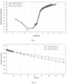
- the OLED had operational voltage 4.8 V, quantum efficiency 5.2 % and current efficiency 5.5 cd/A (see also Figs. 1 and 2 ).
- the lifetime of the OLED expressed as LT97 (the time necessary for luminance decrease to 97 % of its initial value), was 60 hours.
- crosslinked p-doped materials exhibit sufficient conductivity and negligible polymer wash-off and dopant wash-out, they differ in their OLED device performance, especially in terms of lifetime and operational stability.
- crosslinked polymer of the previous application which is formed from precursor polymers having tough backbone requires a stoichiometric excess of acetylenic groups over complementary azide groups (see in Table 1, e.g. better polymer wash-off and dopant wash-out at 3:1 molar ratio)
- more flexible polymers of the present invention enable that the best cross-linking is achieved if the stoichiometric ratio between the complementary groups is set around 1:1, the value which is optimal for OLED operational stability.
- cross-linked p-doped materials with very low content of residual unreacted crosslinking groups. Consequently, cross-linked p-doped materials according to present invention enable designing electronic devices with high reproducibility and favourable stability of their luminance and operational voltage at constant operational current density.
- Figures 1 and 2 compare current-voltage characteristics and lifetime of the blue OLED prepared in the example above (curve (c), circles) and the same OLED prepared under stress conditions of the HTL baking prolonged to 120 minutes (curve (b), rhombi).
- the results show robustness of the inventive doped material, wherein on expense of slightly higher operational voltage, efficiency and device-lifetime can be further increased by prolonged heat treatment of the doped layer, without a substantial change in spectral characteristics of the device.
Landscapes
- Chemical & Material Sciences (AREA)
- Organic Chemistry (AREA)
- Materials Engineering (AREA)
- Engineering & Computer Science (AREA)
- Health & Medical Sciences (AREA)
- Medicinal Chemistry (AREA)
- Polymers & Plastics (AREA)
- Chemical Kinetics & Catalysis (AREA)
- Life Sciences & Earth Sciences (AREA)
- Wood Science & Technology (AREA)
- Emergency Medicine (AREA)
- Physics & Mathematics (AREA)
- Optics & Photonics (AREA)
- Electroluminescent Light Sources (AREA)
Claims (12)
- Matériau semi-conducteur transporteur de charge comprenant :a) éventuellement au moins un dopant électrique etb) un polymère transporteur de charge ramifié ou réticulé comprenant des unités de réticulation 1,2,3-triazole d'au moins une des formules générales la et/ou Ib,dans lequel
 aa) Pol1 à Pol4 sont indépendamment des chaînes choisies du polymère transporteur de charge,bb) X1, X2, X3 et X4 sont des unités d'espaceur choisies indépendamment ou, indépendamment, représentent la liaison directe de Pol1 à Pol4 au cycle 1,2,3-triazole,cc) chacun de R et R' est choisi indépendamment parmi H, un atome d'halogène ou un groupe contenant du carbone,caractérisé en ce qu'au moins un du premier et du second polymères transporteurs de charge précurseurs comprend des unités de construction d'éthylène substituées avec au moins un groupe latéral pendant comprenant un système conjugué d'électrons délocalisés, le nombre moyen de groupes azide et/ou acétyléniques par molécule dans chacun du premier polymère transporteur de charge précurseur, du second polymère transporteur de charge précurseur et de l'agent de réticulation est plus grand que 2, de préférence plus grand que 2,05.le polymère transporteur de charge comprenant des unités de construction d'éthylène substituées avec au moins un groupe latéral pendant comprenant un système conjugué d'électrons délocalisés,le matériau semi-conducteur transporteur de charge pouvant être obtenu par un procédé comprenant les étapes consistant à :i) fournir une solution contenantaaa1) un premier polymère transporteur de charge précurseur comprenant au moins un groupe azide attaché de manière covalente et éventuellement au moins un groupe acétylénique ; et un second polymère transporteur de charge précurseur comprenant au moins un groupe acétylénique attaché de manière covalente et éventuellement au moins un groupe azide ; et éventuellement au moins un agent de réticulation comprenant au moins deux groupes fonctionnels choisis parmi un groupe azide et/ou acétylénique ouaaa2) un premier polymère transporteur de charge comprenant au moins un groupe azide attaché de manière covalente et au moins un groupe acétylénique ; et/ou un second polymère transporteur de charge précurseur comprenant au moins un groupe acétylénique attaché de manière covalente et au moins un groupe azide ; et éventuellement au moins un agent de réticulation comprenant au moins deux groupes fonctionnels choisis parmi un groupe azide et/ou acétylénique,bbb) éventuellement au moins un dopant électrique,ccc) au moins un solvantii) déposer la solution sur un substrat,iii) enlever le solvant etiv) faire réagir les groupes azide et acétylénique pour effectuer une réticulation, de préférence par chauffage,
 - Matériau semi-conducteur transporteur de charge selon la revendication 1, dans lequel, dans le groupe latéral pendant, le système conjugué d'électrons délocalisés est compris dans une fraction structurale carbocyclique ou hétérocyclique.
- Matériau semi-conducteur transporteur de charge selon la revendication 2, dans lequel le système conjugué d'électrons délocalisés compris dans la fraction structurale carboyclique ou hétérocyclique est aromatique.
- Matériau semi-conducteur transporteur de charge selon la revendication 3, dans lequel le groupe latéral pendant comprend au moins deux cycles choisis indépendamment parmi des cycles aromatiques et hétéroaromatiques.
- Matériau semi-condutceur transporteur de charge selon l'une quelconque des revendications 1 à 4, dans lequel le groupe latéral pendant comprend au moins un atome d'azote trivalent.
- Matériau semi-conducteur transporteur de charge selon la revendication 5, dans lequel l'atome d'azote trivalent est substitué avec trois cycles carbocycliques ou hétérocycliques qui sont choisis indépendamment parmi des cycles aromatiques et hétéroaromatiques.
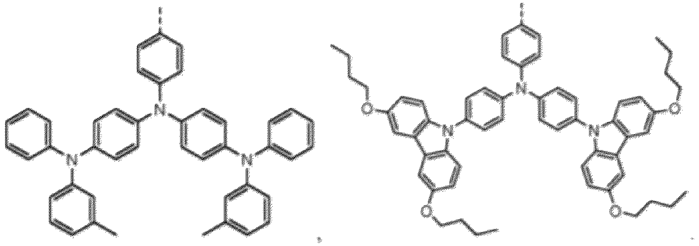
- Matériau semi-conducteur transporteur de charge selon la revendication 6, dans lequel le groupe latéral pendant est choisi parmi

- Matériau semi-conducteur transporteur de charge selon l'une quelconque des revendications précédentes, dans lequel le dopant électrique est un p-dopant.
- Matériau semi-conducteur transporteur de charge selon l'une quelconque des revendications précédentes, dans lequel le dopant électrique est choisi parmi les composés [3]-radialène, chaque atome de carbone de tête de pont étant substitué par un groupe nitrile, un groupe aryle perfluoré en C6 à C14 ou hétéroaryle pefluoré en C2 à C14, jusqu'à trois atomes de fluor dans les substituants perfluorés pouvant être éventuellement remplacés par des groupes choisis indépendamment parmi les groupes nitrile ou trifluorométhyle.
- Polymère transporteur de charge réticulé selon la revendication 1 tel que défini dans l'une quelconque des revendications 1 à 7.
- Procédé de préparation d'un matériau semi-conducteur transporteur de charge selon l'une quelconque des revendications 1 à 9, comprenant les étapes consistant ài) fournir une solution contenanta1) un premier polymère transporteur de charge précurseur comprenant au moins un groupe azide attaché de manière covalente et éventuellement au moins un groupe acétylénique ; et un second polymère transporteur de charge précurseur comprenant au moins un groupe acétylénique attaché de manière covalente et au moins un groupe azide ; et éventuellement au moins un agent de réticulation comprenant au moins deux groupes fonctionnels choisis parmi un groupe azide et/ou acétylénique oua2) un premier polymère transporteur de charge comprenant au moins un groupe azide attaché de manière covalente et au moins un groupe acétylénique ; et/ou un second polymère transporteur de charge précurseur comprenant au moins un groupe acétylénique attaché de manière covalente et au moins un groupe azide ; et éventuellement au moins un agent de réticulation comprenant au moins deux groupes fonctionnels choisis parmi un groupe azide et/ou acétylénique,b) éventuellement au moins un dopant électrique,c) au moins un solvantii) déposer la solution sur un substrat,iii) enlever le solvant etiv) faire réagir les groupes azide et acétylénique pour effectuer une réticulation, de préférence par chauffage,au moins un des premier et second polymères transporteurs de charge précurseurs comprenant des unités de construction d'éthylène substituées avec au moins un groupe latéral pendant comprenant un système conjugué d'électrons délocalisés.
- Dispositif électronique comprenant une couche de semi-conducteur comprenant le matériau semi-conducteur transporteur de charge selon l'une quelconque des revendications 1 à 9.
Priority Applications (3)
| Application Number | Priority Date | Filing Date | Title |
|---|---|---|---|
| EP16156693.0A EP3208862B1 (fr) | 2016-02-22 | 2016-02-22 | Matériau semi-conducteur de transport de charge et dispositif électronique comprenant celui-ci |
| US15/438,378 US10468601B2 (en) | 2016-02-22 | 2017-02-21 | Charge transporting semi-conducting material and electronic device comprising it |
| CN201710097766.XA CN107104191B (zh) | 2016-02-22 | 2017-02-22 | 电荷传输半导体材料和包含它的电子器件 |
Applications Claiming Priority (1)
| Application Number | Priority Date | Filing Date | Title |
|---|---|---|---|
| EP16156693.0A EP3208862B1 (fr) | 2016-02-22 | 2016-02-22 | Matériau semi-conducteur de transport de charge et dispositif électronique comprenant celui-ci |
Publications (2)
| Publication Number | Publication Date |
|---|---|
| EP3208862A1 EP3208862A1 (fr) | 2017-08-23 |
| EP3208862B1 true EP3208862B1 (fr) | 2024-10-09 |
Family
ID=55409774
Family Applications (1)
| Application Number | Title | Priority Date | Filing Date |
|---|---|---|---|
| EP16156693.0A Active EP3208862B1 (fr) | 2016-02-22 | 2016-02-22 | Matériau semi-conducteur de transport de charge et dispositif électronique comprenant celui-ci |
Country Status (3)
| Country | Link |
|---|---|
| US (1) | US10468601B2 (fr) |
| EP (1) | EP3208862B1 (fr) |
| CN (1) | CN107104191B (fr) |
Families Citing this family (4)
| Publication number | Priority date | Publication date | Assignee | Title |
|---|---|---|---|---|
| EP2706584A1 (fr) * | 2012-09-07 | 2014-03-12 | Novaled AG | Matériau semi-conducteur de transport de charge et dispositif semi-conducteur |
| KR102829664B1 (ko) * | 2020-05-06 | 2025-07-07 | 삼성디스플레이 주식회사 | 유기 발광 소자, 유기 발광 소자용 가교제 화합물 및 유기 발광 소자의 제조 방법 |
| JP7764685B2 (ja) * | 2020-09-29 | 2025-11-06 | 株式会社レゾナック | 電荷輸送性材料、インク組成物、有機層、有機エレクトロニクス素子、有機エレクトロルミネセンス素子、照明装置、表示素子、及び表示装置 |
| KR102862545B1 (ko) * | 2021-05-03 | 2025-09-22 | 삼성디스플레이 주식회사 | 발광 소자 및 이의 제조 방법 |
Citations (2)
| Publication number | Priority date | Publication date | Assignee | Title |
|---|---|---|---|---|
| US20070225454A1 (en) * | 2006-03-22 | 2007-09-27 | General Electric Company | Optoelectronic devices with multilayered structures |
| WO2011078391A1 (fr) * | 2009-12-25 | 2011-06-30 | 住友化学株式会社 | Composition et élément luminescent obtenu en utilisant celle-ci |
Family Cites Families (11)
| Publication number | Priority date | Publication date | Assignee | Title |
|---|---|---|---|---|
| US5093698A (en) | 1991-02-12 | 1992-03-03 | Kabushiki Kaisha Toshiba | Organic electroluminescent device |
| JP3960131B2 (ja) | 2002-06-05 | 2007-08-15 | コニカミノルタホールディングス株式会社 | 有機エレクトロルミネッセンス素子材料、及びそれを用いた有機エレクトロルミネッセンス素子および表示装置 |
| AU2004221377B2 (en) | 2003-03-19 | 2009-07-16 | Heliatek Gmbh | Photoactive component comprising organic layers |
| ATE381117T1 (de) | 2005-04-13 | 2007-12-15 | Novaled Ag | Anordnung für eine organische leuchtdiode vom pin-typ und verfahren zum herstellen |
| WO2007071450A1 (fr) | 2005-12-23 | 2007-06-28 | Novaled Ag | Dispositif electronique a structure en couche faite de couches organiques |
| EP1912268B1 (fr) | 2006-10-09 | 2020-01-01 | Novaled GmbH | Méthode de structuration spatiale de l'émission d'une OLED, dispositif organique électroluminescent obtenu par cette méthode, et son usage |
| EP3076451B1 (fr) | 2007-04-30 | 2019-03-06 | Novaled GmbH | Connexions de matiere d'oxydes de carbone, de matiere de pseudo oxyde de carbone et radiales tout comme leur utilisation |
| US8057712B2 (en) | 2008-04-29 | 2011-11-15 | Novaled Ag | Radialene compounds and their use |
| KR101604102B1 (ko) | 2008-09-09 | 2016-03-25 | 테크니온 리서치 엔드 디벨로프먼트 화운데이션 엘티디. | 유기 반도체용의, 유도체화 풀러렌을 주성분으로 하는 도펀트 |
| DE102010027316A1 (de) * | 2010-07-16 | 2012-01-19 | Merck Patent Gmbh | Metallkomplexe |
| EP2706584A1 (fr) * | 2012-09-07 | 2014-03-12 | Novaled AG | Matériau semi-conducteur de transport de charge et dispositif semi-conducteur |
-
2016
- 2016-02-22 EP EP16156693.0A patent/EP3208862B1/fr active Active
-
2017
- 2017-02-21 US US15/438,378 patent/US10468601B2/en active Active
- 2017-02-22 CN CN201710097766.XA patent/CN107104191B/zh active Active
Patent Citations (2)
| Publication number | Priority date | Publication date | Assignee | Title |
|---|---|---|---|---|
| US20070225454A1 (en) * | 2006-03-22 | 2007-09-27 | General Electric Company | Optoelectronic devices with multilayered structures |
| WO2011078391A1 (fr) * | 2009-12-25 | 2011-06-30 | 住友化学株式会社 | Composition et élément luminescent obtenu en utilisant celle-ci |
Also Published As
| Publication number | Publication date |
|---|---|
| CN107104191A (zh) | 2017-08-29 |
| US10468601B2 (en) | 2019-11-05 |
| EP3208862A1 (fr) | 2017-08-23 |
| US20170244033A1 (en) | 2017-08-24 |
| CN107104191B (zh) | 2020-11-03 |
Similar Documents
| Publication | Publication Date | Title |
|---|---|---|
| EP2893576B1 (fr) | Matériau semi-conducteur transporteur de charge et dispositif à semi-conducteur | |
| EP2350166B1 (fr) | Polyarylamine-cétones | |
| Zou et al. | Unexpected Propeller‐Like Hexakis (fluoren‐2‐yl) benzene Cores for Six‐Arm Star‐Shaped Oligofluorenes: Highly Efficient Deep‐Blue Fluorescent Emitters and Good Hole‐Transporting Materials | |
| Cheng et al. | Thermally cross-linkable hole-transporting materials on conducting polymer: synthesis, characterization, and applications for polymer light-emitting devices | |
| US11196009B2 (en) | Fluorene derivative, organic light emitting device using same, and manufacturing method therefor | |
| CN111315796B (zh) | 有机半导体化合物 | |
| KR20110087283A (ko) | 아미노벤젠 조성물 및 관련 소자 및 방법 | |
| CN106084187A (zh) | 聚合物、交联的聚合物以及包含所述聚合物的电致发光器件 | |
| WO2013018951A1 (fr) | Polymère conducteur comprenant du 3,6-carbazole et pile photovoltaïque organique l'utilisant | |
| CN103068878B (zh) | 具有咔唑结构单元的聚合物 | |
| US10468601B2 (en) | Charge transporting semi-conducting material and electronic device comprising it | |
| KR102476916B1 (ko) | 가교결합된 유기 전자 기능층을 갖는 유기 전자 부품 및 상기 부품의 제조에 사용할 수 있는 알키닐 에테르 | |
| EP3961738A1 (fr) | Matériau électronique organique et procédé permettant de préparer un polymère porteur de charge | |
| EP3208863B1 (fr) | Matériau semi-conducteur de transport de charge et dispositif électronique le comprenant | |
| JP2005075913A (ja) | 高分子化合物の製造方法および高分子化合物並びに発光材料 | |
| Chen et al. | Efficient π‐conjugated interrupted host polymer by metal‐free polymerization for blue/green phosphorescent light‐emitting diodes | |
| CN115669267A (zh) | 有机发光器件 | |
| Mazlan | Solution-Processable, Low Work Function N-Doped Organic Semiconductors | |
| JP2008133472A (ja) | 高分子化合物の製造方法および高分子化合物並びに発光材料 |
Legal Events
| Date | Code | Title | Description |
|---|---|---|---|
| PUAI | Public reference made under article 153(3) epc to a published international application that has entered the european phase |
Free format text: ORIGINAL CODE: 0009012 |
|
| STAA | Information on the status of an ep patent application or granted ep patent |
Free format text: STATUS: THE APPLICATION HAS BEEN PUBLISHED |
|
| AK | Designated contracting states |
Kind code of ref document: A1 Designated state(s): AL AT BE BG CH CY CZ DE DK EE ES FI FR GB GR HR HU IE IS IT LI LT LU LV MC MK MT NL NO PL PT RO RS SE SI SK SM TR |
|
| AX | Request for extension of the european patent |
Extension state: BA ME |
|
| STAA | Information on the status of an ep patent application or granted ep patent |
Free format text: STATUS: REQUEST FOR EXAMINATION WAS MADE |
|
| 17P | Request for examination filed |
Effective date: 20171120 |
|
| RBV | Designated contracting states (corrected) |
Designated state(s): AL AT BE BG CH CY CZ DE DK EE ES FI FR GB GR HR HU IE IS IT LI LT LU LV MC MK MT NL NO PL PT RO RS SE SI SK SM TR |
|
| RAP1 | Party data changed (applicant data changed or rights of an application transferred) |
Owner name: FRAUNHOFER GESELLSCHAFT ZUR FOERDERUNG DER ANGEWAN Owner name: NOVALED GMBH |
|
| STAA | Information on the status of an ep patent application or granted ep patent |
Free format text: STATUS: EXAMINATION IS IN PROGRESS |
|
| 17Q | First examination report despatched |
Effective date: 20200827 |
|
| RIC1 | Information provided on ipc code assigned before grant |
Ipc: C08G 73/08 20060101ALN20201126BHEP Ipc: C08F 212/32 20060101ALN20201126BHEP Ipc: H01L 51/46 20060101AFI20201126BHEP Ipc: H01L 51/54 20060101ALI20201126BHEP |
|
| RIC1 | Information provided on ipc code assigned before grant |
Ipc: H01L 51/46 20060101AFI20201202BHEP Ipc: C08G 73/08 20060101ALN20201202BHEP Ipc: H01L 51/54 20060101ALI20201202BHEP Ipc: C08F 212/32 20060101ALN20201202BHEP |
|
| RAP1 | Party data changed (applicant data changed or rights of an application transferred) |
Owner name: NOVALED GMBH |
|
| REG | Reference to a national code |
Ref country code: DE Ref legal event code: R079 Free format text: PREVIOUS MAIN CLASS: H01L0051540000 Ipc: C08F0212140000 Ref country code: DE Ref legal event code: R079 Ref document number: 602016089723 Country of ref document: DE Free format text: PREVIOUS MAIN CLASS: H01L0051540000 Ipc: C08F0212140000 |
|
| GRAP | Despatch of communication of intention to grant a patent |
Free format text: ORIGINAL CODE: EPIDOSNIGR1 |
|
| STAA | Information on the status of an ep patent application or granted ep patent |
Free format text: STATUS: GRANT OF PATENT IS INTENDED |
|
| RIC1 | Information provided on ipc code assigned before grant |
Ipc: C08F 212/14 20060101AFI20240418BHEP Ipc: H10K 50/15 20230101ALN20240418BHEP Ipc: H10K 85/00 20230101ALN20240418BHEP Ipc: H10K 85/60 20230101ALN20240418BHEP Ipc: C08G 73/08 20060101ALN20240418BHEP Ipc: C08F 212/32 20060101ALI20240418BHEP Ipc: H10K 85/10 20230101ALI20240418BHEP |
|
| RIC1 | Information provided on ipc code assigned before grant |
Ipc: H10K 50/15 20230101ALN20240419BHEP Ipc: H10K 85/00 20230101ALN20240419BHEP Ipc: H10K 85/60 20230101ALN20240419BHEP Ipc: C08G 73/08 20060101ALN20240419BHEP Ipc: C08F 212/32 20060101ALI20240419BHEP Ipc: H10K 85/10 20230101ALI20240419BHEP Ipc: C08F 212/14 20060101AFI20240419BHEP |
|
| INTG | Intention to grant announced |
Effective date: 20240513 |
|
| RIC1 | Information provided on ipc code assigned before grant |
Ipc: H10K 50/15 20230101ALN20240502BHEP Ipc: H10K 85/00 20230101ALN20240502BHEP Ipc: H10K 85/60 20230101ALN20240502BHEP Ipc: C08G 73/08 20060101ALN20240502BHEP Ipc: C08F 212/32 20060101ALI20240502BHEP Ipc: H10K 85/10 20230101ALI20240502BHEP Ipc: C08F 212/14 20060101AFI20240502BHEP |
|
| GRAS | Grant fee paid |
Free format text: ORIGINAL CODE: EPIDOSNIGR3 |
|
| GRAA | (expected) grant |
Free format text: ORIGINAL CODE: 0009210 |
|
| STAA | Information on the status of an ep patent application or granted ep patent |
Free format text: STATUS: THE PATENT HAS BEEN GRANTED |
|
| AK | Designated contracting states |
Kind code of ref document: B1 Designated state(s): AL AT BE BG CH CY CZ DE DK EE ES FI FR GB GR HR HU IE IS IT LI LT LU LV MC MK MT NL NO PL PT RO RS SE SI SK SM TR |
|
| REG | Reference to a national code |
Ref country code: CH Ref legal event code: EP |
|
| REG | Reference to a national code |
Ref country code: DE Ref legal event code: R096 Ref document number: 602016089723 Country of ref document: DE |
|
| REG | Reference to a national code |
Ref country code: IE Ref legal event code: FG4D |
|
| P01 | Opt-out of the competence of the unified patent court (upc) registered |
Free format text: CASE NUMBER: APP_53337/2024 Effective date: 20240925 |
|
| REG | Reference to a national code |
Ref country code: LT Ref legal event code: MG9D |
|
| REG | Reference to a national code |
Ref country code: NL Ref legal event code: MP Effective date: 20241009 |
|
| REG | Reference to a national code |
Ref country code: AT Ref legal event code: MK05 Ref document number: 1730531 Country of ref document: AT Kind code of ref document: T Effective date: 20241009 |
|
| PG25 | Lapsed in a contracting state [announced via postgrant information from national office to epo] |
Ref country code: NL Free format text: LAPSE BECAUSE OF FAILURE TO SUBMIT A TRANSLATION OF THE DESCRIPTION OR TO PAY THE FEE WITHIN THE PRESCRIBED TIME-LIMIT Effective date: 20241009 |
|
| PG25 | Lapsed in a contracting state [announced via postgrant information from national office to epo] |
Ref country code: NL Free format text: LAPSE BECAUSE OF FAILURE TO SUBMIT A TRANSLATION OF THE DESCRIPTION OR TO PAY THE FEE WITHIN THE PRESCRIBED TIME-LIMIT Effective date: 20241009 |
|
| PG25 | Lapsed in a contracting state [announced via postgrant information from national office to epo] |
Ref country code: IS Free format text: LAPSE BECAUSE OF FAILURE TO SUBMIT A TRANSLATION OF THE DESCRIPTION OR TO PAY THE FEE WITHIN THE PRESCRIBED TIME-LIMIT Effective date: 20250209 Ref country code: PT Free format text: LAPSE BECAUSE OF FAILURE TO SUBMIT A TRANSLATION OF THE DESCRIPTION OR TO PAY THE FEE WITHIN THE PRESCRIBED TIME-LIMIT Effective date: 20250210 Ref country code: HR Free format text: LAPSE BECAUSE OF FAILURE TO SUBMIT A TRANSLATION OF THE DESCRIPTION OR TO PAY THE FEE WITHIN THE PRESCRIBED TIME-LIMIT Effective date: 20241009 |
|
| PG25 | Lapsed in a contracting state [announced via postgrant information from national office to epo] |
Ref country code: FI Free format text: LAPSE BECAUSE OF FAILURE TO SUBMIT A TRANSLATION OF THE DESCRIPTION OR TO PAY THE FEE WITHIN THE PRESCRIBED TIME-LIMIT Effective date: 20241009 |
|
| PG25 | Lapsed in a contracting state [announced via postgrant information from national office to epo] |
Ref country code: BG Free format text: LAPSE BECAUSE OF FAILURE TO SUBMIT A TRANSLATION OF THE DESCRIPTION OR TO PAY THE FEE WITHIN THE PRESCRIBED TIME-LIMIT Effective date: 20241009 |
|
| PG25 | Lapsed in a contracting state [announced via postgrant information from national office to epo] |
Ref country code: ES Free format text: LAPSE BECAUSE OF FAILURE TO SUBMIT A TRANSLATION OF THE DESCRIPTION OR TO PAY THE FEE WITHIN THE PRESCRIBED TIME-LIMIT Effective date: 20241009 |
|
| PG25 | Lapsed in a contracting state [announced via postgrant information from national office to epo] |
Ref country code: NO Free format text: LAPSE BECAUSE OF FAILURE TO SUBMIT A TRANSLATION OF THE DESCRIPTION OR TO PAY THE FEE WITHIN THE PRESCRIBED TIME-LIMIT Effective date: 20250109 |
|
| PG25 | Lapsed in a contracting state [announced via postgrant information from national office to epo] |
Ref country code: LV Free format text: LAPSE BECAUSE OF FAILURE TO SUBMIT A TRANSLATION OF THE DESCRIPTION OR TO PAY THE FEE WITHIN THE PRESCRIBED TIME-LIMIT Effective date: 20241009 Ref country code: GR Free format text: LAPSE BECAUSE OF FAILURE TO SUBMIT A TRANSLATION OF THE DESCRIPTION OR TO PAY THE FEE WITHIN THE PRESCRIBED TIME-LIMIT Effective date: 20250110 Ref country code: AT Free format text: LAPSE BECAUSE OF FAILURE TO SUBMIT A TRANSLATION OF THE DESCRIPTION OR TO PAY THE FEE WITHIN THE PRESCRIBED TIME-LIMIT Effective date: 20241009 |
|
| PG25 | Lapsed in a contracting state [announced via postgrant information from national office to epo] |
Ref country code: PL Free format text: LAPSE BECAUSE OF FAILURE TO SUBMIT A TRANSLATION OF THE DESCRIPTION OR TO PAY THE FEE WITHIN THE PRESCRIBED TIME-LIMIT Effective date: 20241009 |
|
| PG25 | Lapsed in a contracting state [announced via postgrant information from national office to epo] |
Ref country code: RS Free format text: LAPSE BECAUSE OF FAILURE TO SUBMIT A TRANSLATION OF THE DESCRIPTION OR TO PAY THE FEE WITHIN THE PRESCRIBED TIME-LIMIT Effective date: 20250109 |
|
| PG25 | Lapsed in a contracting state [announced via postgrant information from national office to epo] |
Ref country code: SM Free format text: LAPSE BECAUSE OF FAILURE TO SUBMIT A TRANSLATION OF THE DESCRIPTION OR TO PAY THE FEE WITHIN THE PRESCRIBED TIME-LIMIT Effective date: 20241009 |
|
| PG25 | Lapsed in a contracting state [announced via postgrant information from national office to epo] |
Ref country code: DK Free format text: LAPSE BECAUSE OF FAILURE TO SUBMIT A TRANSLATION OF THE DESCRIPTION OR TO PAY THE FEE WITHIN THE PRESCRIBED TIME-LIMIT Effective date: 20241009 |
|
| REG | Reference to a national code |
Ref country code: DE Ref legal event code: R097 Ref document number: 602016089723 Country of ref document: DE |
|
| PG25 | Lapsed in a contracting state [announced via postgrant information from national office to epo] |
Ref country code: EE Free format text: LAPSE BECAUSE OF FAILURE TO SUBMIT A TRANSLATION OF THE DESCRIPTION OR TO PAY THE FEE WITHIN THE PRESCRIBED TIME-LIMIT Effective date: 20241009 |
|
| PG25 | Lapsed in a contracting state [announced via postgrant information from national office to epo] |
Ref country code: RO Free format text: LAPSE BECAUSE OF FAILURE TO SUBMIT A TRANSLATION OF THE DESCRIPTION OR TO PAY THE FEE WITHIN THE PRESCRIBED TIME-LIMIT Effective date: 20241009 |
|
| PG25 | Lapsed in a contracting state [announced via postgrant information from national office to epo] |
Ref country code: SK Free format text: LAPSE BECAUSE OF FAILURE TO SUBMIT A TRANSLATION OF THE DESCRIPTION OR TO PAY THE FEE WITHIN THE PRESCRIBED TIME-LIMIT Effective date: 20241009 |
|
| PG25 | Lapsed in a contracting state [announced via postgrant information from national office to epo] |
Ref country code: CZ Free format text: LAPSE BECAUSE OF FAILURE TO SUBMIT A TRANSLATION OF THE DESCRIPTION OR TO PAY THE FEE WITHIN THE PRESCRIBED TIME-LIMIT Effective date: 20241009 |
|
| PG25 | Lapsed in a contracting state [announced via postgrant information from national office to epo] |
Ref country code: IT Free format text: LAPSE BECAUSE OF FAILURE TO SUBMIT A TRANSLATION OF THE DESCRIPTION OR TO PAY THE FEE WITHIN THE PRESCRIBED TIME-LIMIT Effective date: 20241009 |
|
| PLBE | No opposition filed within time limit |
Free format text: ORIGINAL CODE: 0009261 |
|
| STAA | Information on the status of an ep patent application or granted ep patent |
Free format text: STATUS: NO OPPOSITION FILED WITHIN TIME LIMIT |
|
| PG25 | Lapsed in a contracting state [announced via postgrant information from national office to epo] |
Ref country code: SE Free format text: LAPSE BECAUSE OF FAILURE TO SUBMIT A TRANSLATION OF THE DESCRIPTION OR TO PAY THE FEE WITHIN THE PRESCRIBED TIME-LIMIT Effective date: 20241009 |
|
| PG25 | Lapsed in a contracting state [announced via postgrant information from national office to epo] |
Ref country code: MC Free format text: LAPSE BECAUSE OF FAILURE TO SUBMIT A TRANSLATION OF THE DESCRIPTION OR TO PAY THE FEE WITHIN THE PRESCRIBED TIME-LIMIT Effective date: 20241009 |
|
| 26N | No opposition filed |
Effective date: 20250710 |
|
| REG | Reference to a national code |
Ref country code: CH Ref legal event code: PL |
|
| PG25 | Lapsed in a contracting state [announced via postgrant information from national office to epo] |
Ref country code: LU Free format text: LAPSE BECAUSE OF NON-PAYMENT OF DUE FEES Effective date: 20250222 |
|
| PG25 | Lapsed in a contracting state [announced via postgrant information from national office to epo] |
Ref country code: CH Free format text: LAPSE BECAUSE OF NON-PAYMENT OF DUE FEES Effective date: 20250228 |
|
| GBPC | Gb: european patent ceased through non-payment of renewal fee |
Effective date: 20250222 |
|
| REG | Reference to a national code |
Ref country code: BE Ref legal event code: MM Effective date: 20250228 |
|
| PG25 | Lapsed in a contracting state [announced via postgrant information from national office to epo] |
Ref country code: GB Free format text: LAPSE BECAUSE OF NON-PAYMENT OF DUE FEES Effective date: 20250222 |
|
| PG25 | Lapsed in a contracting state [announced via postgrant information from national office to epo] |
Ref country code: FR Free format text: LAPSE BECAUSE OF NON-PAYMENT OF DUE FEES Effective date: 20250228 |
|
| PG25 | Lapsed in a contracting state [announced via postgrant information from national office to epo] |
Ref country code: BE Free format text: LAPSE BECAUSE OF NON-PAYMENT OF DUE FEES Effective date: 20250228 |
|
| PG25 | Lapsed in a contracting state [announced via postgrant information from national office to epo] |
Ref country code: IE Free format text: LAPSE BECAUSE OF NON-PAYMENT OF DUE FEES Effective date: 20250222 |
|
| PGFP | Annual fee paid to national office [announced via postgrant information from national office to epo] |
Ref country code: DE Payment date: 20251230 Year of fee payment: 11 |