EP3210352B1 - Appareil et procédé de suppression numérique de diaphonie - Google Patents
Appareil et procédé de suppression numérique de diaphonie Download PDFInfo
- Publication number
- EP3210352B1 EP3210352B1 EP15853162.4A EP15853162A EP3210352B1 EP 3210352 B1 EP3210352 B1 EP 3210352B1 EP 15853162 A EP15853162 A EP 15853162A EP 3210352 B1 EP3210352 B1 EP 3210352B1
- Authority
- EP
- European Patent Office
- Prior art keywords
- signal
- buffer
- pulse
- crosstalk
- summing node
- Prior art date
- Legal status (The legal status is an assumption and is not a legal conclusion. Google has not performed a legal analysis and makes no representation as to the accuracy of the status listed.)
- Active
Links
Images

Classifications
-
- H—ELECTRICITY
- H04—ELECTRIC COMMUNICATION TECHNIQUE
- H04B—TRANSMISSION
- H04B3/00—Line transmission systems
- H04B3/02—Details
- H04B3/32—Reducing cross-talk, e.g. by compensating
-
- G—PHYSICS
- G06—COMPUTING OR CALCULATING; COUNTING
- G06F—ELECTRIC DIGITAL DATA PROCESSING
- G06F13/00—Interconnection of, or transfer of information or other signals between, memories, input/output devices or central processing units
- G06F13/38—Information transfer, e.g. on bus
- G06F13/40—Bus structure
-
- H—ELECTRICITY
- H04—ELECTRIC COMMUNICATION TECHNIQUE
- H04J—MULTIPLEX COMMUNICATION
- H04J1/00—Frequency-division multiplex systems
- H04J1/02—Details
- H04J1/12—Arrangements for reducing cross-talk between channels
-
- H—ELECTRICITY
- H04—ELECTRIC COMMUNICATION TECHNIQUE
- H04J—MULTIPLEX COMMUNICATION
- H04J3/00—Time-division multiplex systems
- H04J3/02—Details
- H04J3/10—Arrangements for reducing cross-talk between channels
-
- H—ELECTRICITY
- H04—ELECTRIC COMMUNICATION TECHNIQUE
- H04L—TRANSMISSION OF DIGITAL INFORMATION, e.g. TELEGRAPHIC COMMUNICATION
- H04L25/00—Baseband systems
- H04L25/02—Details ; arrangements for supplying electrical power along data transmission lines
- H04L25/0264—Arrangements for coupling to transmission lines
- H04L25/0292—Arrangements specific to the receiver end
-
- H—ELECTRICITY
- H04—ELECTRIC COMMUNICATION TECHNIQUE
- H04L—TRANSMISSION OF DIGITAL INFORMATION, e.g. TELEGRAPHIC COMMUNICATION
- H04L25/00—Baseband systems
- H04L25/02—Details ; arrangements for supplying electrical power along data transmission lines
- H04L25/08—Modifications for reducing interference; Modifications for reducing effects due to line faults ; Receiver end arrangements for detecting or overcoming line faults
-
- H—ELECTRICITY
- H04—ELECTRIC COMMUNICATION TECHNIQUE
- H04L—TRANSMISSION OF DIGITAL INFORMATION, e.g. TELEGRAPHIC COMMUNICATION
- H04L25/00—Baseband systems
- H04L25/02—Details ; arrangements for supplying electrical power along data transmission lines
- H04L25/14—Channel dividing arrangements, i.e. in which a single bit stream is divided between several baseband channels and reassembled at the receiver
Definitions
- FEXT Far End Crosstalk
- I/O input-output
- MTs Mega Transfers
- DDR4 Double Data Rate 4
- LPDDR4 Low Power DD44
- JEDEC Joint Electron Device Council
- first buffer to receive a first signal from a first transmission media
- second buffer to receive a second signal from a second transition media separate from the first transition media
- first summing node coupled to the first buffer
- the first summing node to receive output of the first buffer
- a first digital adjustment circuit which is operable to a drive a first adjustment signal to the first summing node when a transition edge of the second signal is detected.
- Some method and apparatus for cancelling FEXT resorts to analog filtering circuitry that extracts the aggressor's FEXT contribution and proportionally removes it from the victim signal.
- the aggressor signal passes through a differentiator (or high pass filter) at the Rx to emulate the channel inductive coupling effect. This emulation process results in generating an artificially recreated signal which is an inverse version of the FEXT and is summed to a victim lane signal to generate a FEXT-free signal at the summer output.
- FEXT degrades timing margin rather than voltage margin.
- an apparatus is described which regains this lost timing margin by performing timing adjustment (e.g., pull-in or push-out) of the victim signal edge transition based on the aggressor signals' edge transition.
- the apparatus includes circuits that first detect the polarity of crosstalk, and then cancel the jitter. In some embodiments, this cancellation of crosstalk is implemented using all digital circuits with Complementary Metal Oxide Semiconductor (CMOS) level signaling.
- CMOS Complementary Metal Oxide Semiconductor
- the cross-coupled apparatus for cancelling FEXT comprises digital circuits that consume substantially less energy than traditional high precession analog circuits used for cancelling FEXT.
- the circuits being digital in nature also scale well with process nodes compared to analog circuits that require a complete redesign with any shift in process parameters.
- the cross-coupled apparatus of various embodiments widens the eye width of an eye diagram without the expense of high power analog circuits.
- signals are represented with lines. Some lines may be thicker, to indicate more constituent signal paths, and/or have arrows at one or more ends, to indicate primary information flow direction. Such indications are not intended to be limiting. Rather, the lines are used in connection with one or more exemplary embodiments to facilitate easier understanding of a circuit or a logical unit. Any represented signal, as dictated by design needs or preferences may actually comprise one or more signals that may travel in either direction and may be implemented with any suitable type of signal scheme.
- connection means a direct electrical or wireless connection between the things that are connected, without any intermediary devices.
- coupled means either a direct electrical or wireless connection between the things that are connected or an indirect connection through one or more passive or active intermediary devices.
- circuit means one or more passive and/or active components that are arranged to cooperate with one another to provide a desired function.
- signal means at least one current signal, voltage signal or data/clock signal.
- scaling generally refers to converting a design (schematic and layout) from one process technology to another process technology and subsequently being reduced in layout area.
- scaling generally also refers to downsizing layout and devices within the same technology node.
- scaling may also refer to adjusting (e.g., slowing down or speeding up - i.e. scaling down, or scaling up respectively) of a signal frequency relative to another parameter, for example, power supply level.
- substantially “close,” “approximately,” “near,” and “about,” generally refer to being within +/- 20% of a target value.
- the transistors in various circuits and logic blocks are metal oxide semiconductor (MOS) transistors, which include drain, source, gate, and bulk terminals.
- MOS metal oxide semiconductor
- the transistors also include Tri-Gate and FinFET transistors, Gate All Around Cylindrical Transistors, Tunneling FET (TFET), Square Wire, or Rectangular Ribbon Transistors or other devices implementing transistor functionality like carbon nano tubes or spintronic devices.
- MOSFET symmetrical source and drain terminals i.e., are identical terminals and are interchangeably used here.
- a TFET device has asymmetric Source and Drain terminals.
- MOSFET Bi-polar junction transistors-BJT PNP/NPN, BiCMOS, CMOS, eFET, etc.
- MN indicates an n-type transistor (e.g., NMOS, NPN BJT, etc.) and the term “MP” indicates a p-type transistor (e.g., PMOS, PNP BJT, etc.).
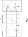
- Fig. 1 illustrates a system 100 having digital crosstalk cancelling apparatus, according to some embodiments of the disclosure.
- system 100 comprises Processor-1 101 (e.g., memory controller, graphics processor, general processor, digital signal processor, etc.), Transmission Media 102 (e.g., on-die or off-die interconnect, transmission lines, etc.), and Processor-2 103 (e.g., Dynamic Random Access Memory (DRAM), or any other processor) having apparatus for cancelling FEXT or other types of crosstalk.
- Transmission Media 102 may be a cable with tightly packed wires such that data on one wire may cause noise on data being carried by other wires within the packet.
- Transmission Media 102 is a parallel bus with closely spaced interconnects.
- Processor-1 101 comprises many circuits including transmitters (Tx) that drive data on Transmission Media 102 to Processor-2 102.
- Tx transmitters
- Transmission Media 102 is shown with three transmission lines (TL)-TL1 to TL3.
- One end of the TLs are coupled to output ports of Tx of Processor-1 101 and the other end of TLs are coupled to input ports of receivers (Rx) of Processor-2 103.
- TL1 is coupled on one end to Port1 and at another end to Port1a;
- TL2 (not shown) is coupled on one end to Port2 (not shown) and at another end to Port2a;
- TL3 is coupled on one end to Port3 and at another end to Port3a, and so on.
- Processor-2 103 includes receivers that receive data transmitted by transmitters.
- three receivers are shown-Rx1 to Rx3-that receive data from respective input ports.
- each receiver also receives data from neighboring receivers.
- Rx1 receives data from Portia and Port3a so that it may cancel crosstalk on data on either ports caused by an attacker on either Portia or Port3a.
- data on TL3 induces FEXT on data on TL1
- data on TL3 is considered the attacker and data on TL1 is considered a victim, and vice versa.
- each receiver includes digital crosstalk cancelling apparatus (or module) 110.
- crosstalk free (or crosstalk reduced) data is then sent to sampling flops (or sequential logic) for further processing.
- Time-of-Flight (TOF) of a signal can be determined by a nominal time T (i.e., without crosstalk interference), and an additional component due to even or odd mode crosstalk.
- Sign or polarity of the crosstalk jitter can be determined by the transmission line characteristic, or whether the line is dominated by mutual inductance L or capacitance C, referred as inductive or capacitive crosstalk respectively.
- this additional jitter term can be cancelled using delay compensation circuits according to some embodiments.
- the apparatus regains this lost timing margin by performing timing adjustment (e.g., pull-in or push-out) of the victim signal edge transition based on the aggressor's transition by first detecting the polarity of crosstalk, and then cancelling the jitter.
- timing adjustment e.g., pull-in or push-out
- Compensation polarity can be determined a priori by the characteristic of the physical interconnect. For example, it can be determined by pre-silicon or post-silicon debug whether the interconnects are inductive dominant or capacitance dominant (i.e., inductive when L m /Z o> C m Z o ; capacitive when L m /Z o ⁇ C m Z o ).
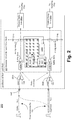
- Fig. 2 illustrates a portion 200 of system 100 having digital apparatus 201 (which includes 110 of Rx1 and 110 of Rx3) for crosstalk cancellation, according to some embodiments of the disclosure. It is pointed out that those elements of Fig. 2 having the same reference numbers (or names) as the elements of any other figure can operate or function in any manner similar to that described, but are not limited to such.
- portion 200 comprises input amplifiers (Amp) and digital apparatus 201.
- Amp 202a is part of Rx1 while Amp 202b is part of Rx3.
- digital apparatus 201 comprises delay matched buffers 203a and 203b, Victim/Aggressor Buffers 204a and 204b, Deskew Delay Lines 205a and 205b, capacitive devices Cma and Cmb, and cross-coupled crosstalk detectors and correctors 206a and 206b coupled together as shown.
- each Rx receives at least two inputs-one from a TL driven by a corresponding Tx and another from a neighboring TL, which is driven by another Tx.
- TL3 is the aggressor and TL1 is the victim (i.e., data transmitted on TL3 is the aggressor data, and data transmitted on TL1 is the victim data).
- victim data i.e., data1
- Amp 202a which compares data1 with a reference voltage (Vref).
- Vref reference voltage
- the output of Amp 202a is received by delay buffer 203a which delays the output of Amp 202a and provides it to node na.
- nodes and signals are interchangeably used. For example, "na” may refer to node na or signal na depending on the context of the sentence.
- Buffer 204a (also referred to here as Victim Buffer).
- output of Buffer 204a is provided to mixing node n1 (also referred here as the first summing node).
- Aggressor data i.e., data2
- Amp 202b which compares data2 with Vref.
- the output of Amp 202b is received by delay buffer 203b, which delays the output of Amp 202b and provides it to node nb.
- delay buffers 203a and 203b have matched delays (i.e., substantially equal propagation delays).
- the signal on node nb is then buffered by Buffer 204b (also referred here as the Aggressor Buffer).
- Buffer 204b also referred here as the Aggressor Buffer.
- output of Buffer 204b is provided to mixing node n2 (also referred to here as the second summing node).
- Signals on mixing nodes n1 and n2 are then provided to Deskew Delay Lines 205a and 205b, respectively.
- Deskew Delay Lines 205a and 205b may be used to realign data on mixing nodes n1 and n2 relative to a clock signal for subsequent sampling by downstream sequential logic (not shown).
- cross-coupled crosstalk detectors and correctors 206a and 206b are used to cancel or reduce crosstalk on data1 and/or data2 (depending on which one is the aggressor and victim) by subtracting or adding signals on mixing nodes n1 and n2.
- crosstalk detector and corrector 206a i.e., crosstalk detector and corrector 110 of Rx1
- crosstalk detector and corrector 206b comprises Pulse Generator 207, Correction Buffer 208, and Mode logic.
- crosstalk detector and corrector 206b i.e., crosstalk detector and corrector 110 of Rx3 has the same design as crosstalk detector and corrector 206a but with different inputs.
- crosstalk detector and corrector 206a receives input on node nb and provides an output which is summed at mixing node n1 while crosstalk detector and corrector 206b receives input on node na and provides an output which is summed at mixing node n2. So as not to obscure the embodiments, crosstalk detector and corrector 206a is described, and similar explanation is applicable for crosstalk detector and corrector 206b.
- Pulse Generator 207 provides an enable/disable pulse to Correction Buffer 208.
- Correction Buffer 208 receives input on node nb (i.e., the aggressor signal) and generates an output for summing on the mixing node n1 when Pulse Generator 207 identifies the transition edge of the signal on node nb.
- the pulse width of the pulse generated by Pulse Generator 207 is programmable and/or adjustable to cause Correction Buffer 208 to turn on (i.e., become enabled) when the aggressor signal is transitioning.
- capacitive devices Cma and Cmb are coupled to mixing nodes n1 and n2, respectively, to improve the process of summing or mixing induced delay adjustment.
- capacitive devices Cma and Cmb are metal capacitors.
- capacitive devices Cma and Cmb are implemented as transistors.
- capacitive devices Cma and Cmb are implemented as hybrid capacitors (i.e., a mix of metal capacitors and transistors).
- Correction Buffer 208 is enabled during an attacker's edge transition.
- the strength of Correction Buffer 208 is programmable to proportionally control the timing adjustment through the capacitive device Cma at the mixing node n1.
- the delay adjustment provided by the mixing scheme can fully cancel the crosstalk induced jitter.
- the polarity of the output of crosstalk detector and corrector 206a (and 206b) can be determined. For example, when both the aggressor and victim signals (i.e., data2 and data1, respectively) transition in the same direction (i.e., both transition from high to low or low to high), then the mode is an even mode. In inductive crosstalk, even mode crosstalk slows down the propagation of a signal transition, while odd mode crosstalk speeds up propagation of a signal transition. In capacitive crosstalk, even mode crosstalk speeds up the propagation of a signal transition, while odd mode crosstalk slows down the propagation.
- a Mode Select signal (shown with reference to Fig. 3A ) is asserted (i.e., configured to logic high) to cause Mode logic to provide an inverted version of the signal on node na/nb as input to the Correction Buffer 208 which is designed to be an inverting buffer.
- Mode Select indicates the coupling nature of the physical transmission media, (i.e., whether the physical transmission media is capacitive dominated or inductive dominated).
- the output of Correction Buffer 208 of crosstalk detector and corrector 206a is summed or mixed with the output of Buffer 204a on the mixing node n1 such that the victim signal at Buffer 204a output is sped up or slowed down in the reverse manner as the upstream inductive FEXT effect, achieving the cancellation result.
- Table 1 summarizes the output signal behavior of Correction Buffer 208 in crosstalk even/odd modes and in crosstalk inductive/capacitive modes.
- Table 1: FEXT effect is summarized by the four cases Even Odd Inductive Slow down Speed up Capacitive Speed up Slow down
- Fig. 3A illustrates apparatus 300 (e.g., 206a/b) for crosstalk detection and correction, according to some embodiments of the disclosure. It is pointed out that those elements of Fig. 3A having the same reference numbers (or names) as the elements of any other figure can operate or function in any manner similar to that described, but are not limited to such.
- apparatus 300 comprises Pulse Generator 207, Mode logic, and Correction Buffer 208.
- Pulse Generator 207 comprises an exclusive-OR logic gate (XOR) 301 coupled to variable delay buffer 302.
- the output of Pulse Generator 207 is an Enable signal that enables Correction Buffer 208.
- the XOR gate 301 compares the signal on node na/nb with a delayed version of that signal (i.e., delayed by variable delay buffer 302) to generate a pulse (i.e., Enable signal).
- the pulse width of the Enable signal can be adjusted. If the aggressor and victim transitions have a skew exceeding the propagation delay of buffer 302, crosstalk jitter diminishes. In such a case, there may be no need to activate or enable Correction Buffer 208.
- Propagation delay of buffer 302 for a DDR4 channel may be set around 50ps. While the embodiments are described with reference to an XOR based Pulse Generator 207, other implementations of Pulse Generator 207 may be used without departing from the essence of some embodiments.
- output of Correction Buffer 208 is received by mixing nodes n1/n2.
- Mode logic comprises Inverter 209 and Multiplexer 210.
- input "Out" of Correction Buffer 208 is inverted depending on the Mode Select signal. For example, when the victim and aggressor signals on nodes na and nb, respectively, are in even mode, then Mode Select is asserted and Multiplexer 210 selects output of inverter 209 as Out signal (i.e., input of Correction Buffer 208).
- the Mode Select signal configures the circuit to work in either inductive or capacitive interconnection environment.
- the Mode Select signal is a static control or configuration.
- the circuit once configured by the Mode Select signal, the circuit handles the even/odd mode crosstalk signal automatically (i.e., no other control is used to dynamically detect the even/odd crosstalk).
- Mode Select is de-asserted and Multiplexer 210 selects signals on node na/nb as Out signal (i.e., input of Correction Buffer 208).
- the propagation delay of crosstalk detection and correction apparatus 300 is matched with the propagation delay of buffers 204a/204b.
- Fig. 3B illustrates Correction Buffer 320 (e.g., 208) used in Fig. 3A , according to some embodiments of the disclosure. It is pointed out that those elements of Fig. 3B having the same reference numbers (or names) as the elements of any other figure can operate or function in any manner similar to that described, but are not limited to such.
- Correction Buffer 320 e.g., 208
- Correction Buffer 320 comprises p-type devices MP1 and MP2, n-type devices MN1 and MN2, and inverter 321 coupled together as shown.
- signals on nodes na/nb are used to control gate terminals of MP1 and MN1.
- the Enable signal and its inverted version are used to control the gate terminals of MN2 and MP2, respectively.
- the input of Correction Buffer 320 is "Out" which is the output of Mode logic.
- the output of Correction Buffer 320 is Out b, which in some embodiments is provided directly to the mixing node.
- the strength of Correction Buffer 320, and hence the propagation delay is adjustable by adding or subtracting transistors in parallel to MP1 and MN1.
- pull-up (or pull down) strength (or effective resistance R) of Buffers 204a and/or 204b is modulated to be weaker or stronger providing delay adjustment as the victim signal passes through.
- Fig. 3C illustrates an example 330 of Buffers 204a/204b.
- Buffers 204a/204b comprise p-type transistors MP1 coupled in series with n-type transistors MN1 as shown. While example 330 shows one p-type transistor MP1 and one n-type transistor MN1, multiple transistors are coupled in parallel. For example, multiple p-type transistors are coupled in parallel to MP1 and are controllable by control signals (not shown).
- the gate terminals of MP1 and MN1 are coupled to nodes na/nb and drain terminals of MP1 and MN1 are coupled to nodes n1/n2.
- the source terminals of MP1 are coupled to power supply Vcc while the source terminals of MN1 are coupled to ground.
- the pull-up (or pull down) strength (or effective resistance R) of the Buffers 204a/204b, and hence their propagation delay is adjusted by turning on/off transistors (i.e., the parallel transistors coupled to MP1 and MN1).
- Buffers 204a and/or 204b have matched propagation delays.
- Buffers 204a and/or 204b have programmable and/or adjustable delays.
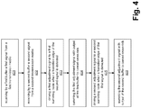
- Fig. 4 illustrates a flowchart 400 of a method to cancel or reduce crosstalk using the digital apparatus for crosstalk cancellation, according to some embodiments of the disclosure. It is pointed out that those elements of Fig. 4 having the same reference numbers (or names) as the elements of any other figure can operate or function in any manner similar to that described, but are not limited to such.
- a first buffer receives a first signal (e.g., signal on node na). This first signal is received from a first transmission media (e.g., TL1 of Transmission Media 102) after being compared by Amp 202a and delayed by buffer 203a.
- a second buffer receives a second signal (e.g., signal on node nb). This second signal is received from a second transmission media (e.g., TL3 of Transmission Media 102) after being compared by Amp 202b and delayed by Buffer 203b.
- crosstalk detection and correction apparatus 206a generates a first adjustment signal (also referred here as the contention or auxiliary signal), which is driven on to the mixing node n1 (also referred here as the summing node) when Pulse Generator 207 of apparatus 206a detects transition edge of the second signal (i.e., signal on node nb).
- the output of Buffer 204a is summed with the first adjustment signal to cancel crosstalk-timing jitter from the output of Buffer 204a.
- crosstalk detection and correction apparatus 206b generates a second adjustment signal, which is driven on to the mixing node n2 (also referred to here as the summing node) when Pulse Generator 207 of 206b detects transition edge of the first signal (i.e., signal on node na).
- output of buffer 204b is summed with the second adjustment signal to cancel crosstalk from the output of buffer 204b. Subsequent downstream logic then processes the signals with cancelled crosstalk.
- Supply noise-induced jitter may increase due to slow signal slope at the summing nodes n1 and 2.
- the signals on the summing nodes n1 and n2 may experience "blips" (i.e., transient voltage/current droops or spikes) when the victim signal is DC during the transitions of the aggressor signal transitions due to the contention event.
- the buffer (not shown) after nodes n1 and n2 are used to filter these blips.
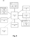
- Fig. 5 illustrates a smart device or a computer system or a SoC (System-on-Chip) with digital crosstalk cancelling apparatus, according to some embodiments. It is pointed out that those elements of Fig. 5 having the same reference numbers (or names) as the elements of any other figure can operate or function in any manner similar to that described, but are not limited to such.
- Fig. 5 illustrates a block diagram of an embodiment of a mobile device in which flat surface interface connectors could be used.
- computing device 1600 represents a mobile computing device, such as a computing tablet, a mobile phone or smart-phone, a wireless-enabled e-reader, or other wireless mobile device. It will be understood that certain components are shown generally, and not all components of such a device are shown in computing device 1600.
- computing device 1600 includes a first processor 1610 with digital crosstalk cancelling apparatus, according to some embodiments discussed.
- Other blocks of the computing device 1600 may also include the digital crosstalk cancelling apparatus of some embodiments.
- the various embodiments of the present disclosure may also comprise a network interface within 1670 such as a wireless interface so that a system embodiment may be incorporated into a wireless device, for example, cell phone or personal digital assistant.
- processor 1610 can include one or more physical devices, such as microprocessors, application processors, microcontrollers, programmable logic devices, or other processing means.
- the processing operations performed by processor 1610 include the execution of an operating platform or operating system on which applications and/or device functions are executed.
- the processing operations include operations related to I/O (input/output) with a human user or with other devices, operations related to power management, and/or operations related to connecting the computing device 1600 to another device.
- the processing operations may also include operations related to audio I/O and/or display I/O.
- computing device 1600 includes audio subsystem 1620, which represents hardware (e.g., audio hardware and audio circuits) and software (e.g., drivers, codecs) components associated with providing audio functions to the computing device. Audio functions can include speaker and/or headphone output, as well as microphone input. Devices for such functions can be integrated into computing device 1600, or connected to the computing device 1600. In one embodiment, a user interacts with the computing device 1600 by providing audio commands that are received and processed by processor 1610.
- audio subsystem 1620 represents hardware (e.g., audio hardware and audio circuits) and software (e.g., drivers, codecs) components associated with providing audio functions to the computing device. Audio functions can include speaker and/or headphone output, as well as microphone input. Devices for such functions can be integrated into computing device 1600, or connected to the computing device 1600. In one embodiment, a user interacts with the computing device 1600 by providing audio commands that are received and processed by processor 1610.
- Display subsystem 1630 represents hardware (e.g., display devices) and software (e.g., drivers) components that provide a visual and/or tactile display for a user to interact with the computing device 1600.
- Display subsystem 1630 includes display interface 1632, which includes the particular screen or hardware device used to provide a display to a user.
- display interface 1632 includes logic separate from processor 1610 to perform at least some processing related to the display.
- display subsystem 1630 includes a touch screen (or touch pad) device that provides both output and input to a user.
- I/O controller 1640 represents hardware devices and software components related to interaction with a user. I/O controller 1640 is operable to manage hardware that is part of audio subsystem 1620 and/or display subsystem 1630. Additionally, I/O controller 1640 illustrates a connection point for additional devices that connect to computing device 1600 through which a user might interact with the system. For example, devices that can be attached to the computing device 1600 might include microphone devices, speaker or stereo systems, video systems or other display devices, keyboard or keypad devices, or other I/O devices for use with specific applications such as card readers or other devices.
- I/O controller 1640 can interact with audio subsystem 1620 and/or display subsystem 1630.
- input through a microphone or other audio device can provide input or commands for one or more applications or functions of the computing device 1600.
- audio output can be provided instead of, or in addition to display output.
- display subsystem 1630 includes a touch screen
- the display device also acts as an input device, which can be at least partially managed by I/O controller 1640.
- I/O controller 1640 manages devices such as accelerometers, cameras, light sensors or other environmental sensors, or other hardware that can be included in the computing device 1600.
- the input can be part of direct user interaction, as well as providing environmental input to the system to influence its operations (such as filtering for noise, adjusting displays for brightness detection, applying a flash for a camera, or other features).
- computing device 1600 includes power management 1650 that manages battery power usage, charging of the battery, and features related to power saving operation.
- Memory subsystem 1660 includes memory devices for storing information in computing device 1600. Memory can include nonvolatile (state does not change if power to the memory device is interrupted) and/or volatile (state is indeterminate if power to the memory device is interrupted) memory devices. Memory subsystem 1660 can store application data, user data, music, photos, documents, or other data, as well as system data (whether long-term or temporary) related to the execution of the applications and functions of the computing device 1600.
- Elements of embodiments are also provided as a machine-readable medium (e.g., memory 1660) for storing the computer-executable instructions (e.g., instructions to implement any other processes discussed herein).
- the machine-readable medium e.g., memory 1660
- embodiments of the disclosure may be downloaded as a computer program (e.g., BIOS), which may be transferred from a remote computer (e.g., a server) to a requesting computer (e.g., a client) by way of data signals via a communication link (e.g., a modem or network connection).
- BIOS a computer program
- a remote computer e.g., a server
- a requesting computer e.g., a client
- a communication link e.g., a modem or network connection
- Connectivity 1670 includes hardware devices (e.g., wireless and/or wired connectors and communication hardware) and software components (e.g., drivers, protocol stacks) to enable the computing device 1600 to communicate with external devices.
- the computing device 1600 could be separate devices, such as other computing devices, wireless access points or base stations, as well as peripherals such as headsets, printers, or other devices.
- Connectivity 1670 can include multiple different types of connectivity.
- the computing device 1600 is illustrated with cellular connectivity 1672 and wireless connectivity 1674.
- Cellular connectivity 1672 refers generally to cellular network connectivity provided by wireless carriers, such as provided via GSM (global system for mobile communications) or variations or derivatives, CDMA (code division multiple access) or variations or derivatives, TDM (time division multiplexing) or variations or derivatives, or other cellular service standards.
- Wireless connectivity (or wireless interface) 1674 refers to wireless connectivity that is not cellular, and can include personal area networks (such as Bluetooth, Near Field, etc.), local area networks (such as Wi-Fi), and/or wide area networks (such as WiMax), or other wireless communication.
- Peripheral connections 1680 include hardware interfaces and connectors, as well as software components (e.g., drivers, protocol stacks) to make peripheral connections. It will be understood that the computing device 1600 could both be a peripheral device ("to" 1682) to other computing devices, as well as have peripheral devices ("from” 1684) connected to it.
- the computing device 1600 commonly has a "docking" connector to connect to other computing devices for purposes such as managing (e.g., downloading and/or uploading, changing, synchronizing) content on computing device 1600. Additionally, a docking connector can allow computing device 1600 to connect to certain peripherals that allow the computing device 1600 to control content output, for example, to audiovisual or other systems.
- the computing device 1600 can make peripheral connections 1680 via common or standards-based connectors.
- Common types can include a Universal Serial Bus (USB) connector (which can include any of a number of different hardware interfaces), DisplayPort including MiniDisplayPort (MDP), High Definition Multimedia Interface (HDMI), Firewire, or other types.
- USB Universal Serial Bus
- MDP MiniDisplayPort
- HDMI High Definition Multimedia Interface
- Firewire or other types.
- first embodiment may be combined with a second embodiment anywhere the particular features, structures, functions, or characteristics associated with the two embodiments are not mutually exclusive.
- DRAM Dynamic RAM
- an apparatus which comprises: a first buffer to receive a first signal from a first transmission media; a second buffer to receive a second signal from a second transmission media separate from the first transmission media; a first summing node coupled to the first buffer, the first summing node to receive output of the first buffer; and a first digital adjustment circuit which is operable to drive a first adjustment signal to the first summing node when a transition edge of the second signal is detected.
- the first buffer and the first digital adjustment circuit have substantially the same propagation delays.
- the first digital adjustment circuit comprises: a pulse generator to receive the second signal and to generate a pulse; and a tri-state buffer which is operable to buffer the second signal as the first adjustment signal according to a duration of the pulse.
- the pulse generator has a programmable delay buffer.
- the apparatus comprises: a second summing node coupled to the second buffer, the second summing node to receive output of the second buffer.
- the apparatus comprises: a second digital adjustment circuit which is operable to drive a second adjustment signal to the second summing node when a transition edge of the first signal is detected.
- the apparatus comprises: a first capacitive device coupled to the first summing node; and a second capacitive device coupled to the second summing node.
- the second buffer and the second digital adjustment circuit have substantially the same propagation delays.
- the second digital adjustment circuit comprises: a pulse generator to receive the first signal and to generate a pulse; and a tri-state buffer which is operable to buffer the first signal as the second adjustment signal according to a duration of the pulse.
- the pulse generator has a programmable delay buffer.
- an apparatus which comprises: a bus to provide first and second signals; and a pair of cross-coupled digital adjustment circuits which are operable to: drive a first adjustment signal to a first summing node when a transition edge of the second signal is detected, and drive a second adjustment signal to a second summing node when a transition edge of the first signal is detected.
- one of the cross-coupled digital adjustment circuit comprises: a pulse generator to receive the second signal and to generate a pulse; and a tri-state buffer which is operable to buffer the second signal as the first adjustment signal according to a duration of the pulse.
- another of the cross-coupled digital adjustment circuit comprises: a pulse generator to receive the first signal and to generate a pulse; and a tri-state buffer which is operable to buffer the first signal as the second adjustment signal according to a duration of the pulse.
- the apparatus comprises: a first buffer to receive the first signal from a first transmission media of the bus; and a second buffer to receive a second signal from a second transmission media of the bus, the second transmission media separate from the first transmission media.
- a system which comprises: a memory; a processor coupled to the memory by a bus having first and second transmission lines to provide first and second signals respectively, the processor including a receiver which comprises: a pair of cross-coupled digital adjustment circuits which are operable to: drive a first adjustment signal to a first summing node when a transition edge of the second signal is detected, and drive a second adjustment signal to a second summing node when a transition edge of the first signal is detected; and a wireless interface for allowing the processor to communicate with another device.
- the receiver is a Double Data Rate (DDR) compliant receiver.
- one of the cross-coupled digital adjustment circuit comprises: a pulse generator to receive the second signal and to generate a pulse; and a tri-state buffer which is operable to buffer the second signal as the first adjustment signal according to a duration of the pulse.
- another of the cross-coupled digital adjustment circuit comprises: a pulse generator to receive the first signal and to generate a pulse; and a tri-state buffer which is operable to buffer the first signal as the second adjustment signal according to a duration of the pulse.
- the receiver comprises: a first buffer to receive the first signal from a first transmission media of the bus; and a second buffer to receive a second signal from a second transmission media of the bus, the second transmission media separate from the first transmission media.
- the system further comprises a display interface for allowing a display unit to display content processed by the processor.
- a method which comprises: receiving first and second signals; driving a first adjustment signal to a first summing node when a transition edge of the second signal is detected, and driving a second adjustment signal to a second summing node when a transition edge of the first signal is detected.
- the method comprises generating a pulse using the second signal.
- the method comprises buffering the second signal as the first adjustment signal according to a duration of the pulse.
- the method comprises generating a pulse using the first signal.
- the method comprises: buffering the first signal as the second adjustment signal according to a duration of the pulse.
- the method comprises: receiving the first signal from a first transmission media.
- the method comprises: receiving the second signal from a second transmission media of the bus, the second transmission media being separate from the first transmission media.
- an apparatus which comprises: means for receiving first and second signals; means for driving a first adjustment signal to a first summing node when a transition edge of the second signal is detected, and means for driving a second adjustment signal to a second summing node when a transition edge of the first signal is detected.
- the apparatus comprises: means for generating a pulse using the second signal.
- the apparatus comprises: means for buffering the second signal as the first adjustment signal according to a duration of the pulse.
- the apparatus comprises: means for generating a pulse using the first signal.
- the apparatus comprises: means for buffering the first signal as the second adjustment signal according to a duration of the pulse. In some embodiments, the apparatus comprises: means for receiving the first signal from a first transmission media. In some embodiments, the apparatus comprises: means for receiving the second signal from a second transmission media of the bus, the second transmission media being separate from the first transmission media.
- a system which comprises: a memory; a processor coupled to the memory by a bus having first and second transmission lines to provide first and second signals respectively, the processor including a receiver which comprises an apparatus according to the apparatus described above; and a wireless interface for allowing the processor to communicate with another device.
- the system further comprises a display interface for allowing a display unit to display content processed by the processor.
Landscapes
- Engineering & Computer Science (AREA)
- Computer Networks & Wireless Communication (AREA)
- Signal Processing (AREA)
- Power Engineering (AREA)
- General Engineering & Computer Science (AREA)
- Theoretical Computer Science (AREA)
- Computer Hardware Design (AREA)
- Physics & Mathematics (AREA)
- General Physics & Mathematics (AREA)
- Design And Manufacture Of Integrated Circuits (AREA)
Claims (11)
- Appareil (201), comprenant :un premier tampon (204a) pour recevoir un premier signal d'un premier support de transmission (TL1) ;un deuxième tampon (204b) pour recevoir un deuxième signal d'un deuxième support de transmission (TL3) séparé du premier support de transmission (TL1) ;un premier nœud de sommation (n1) couplé au premier tampon (204a), le premier nœud de sommation étant destiné à recevoir une sortie du premier tampon ;un premier circuit de réglage numérique qui est opérationnel pour amener un premier signal de réglage au premier nœud de sommation (n1) lorsqu'un flanc de transition du deuxième signal est détecté, le premier circuit de réglage numérique comprenant :un générateur d'impulsion (207) destiné à recevoir le deuxième signal et à générer une impulsion lorsqu'un flanc de transition du deuxième signal est détecté ; etun tampon à trois états qui est opérationnel pour mettre le deuxième signal en mémoire tampon en tant que premier signal de réglage selon une durée de l'impulsion lorsqu'un flanc de transition du deuxième signal est détecté ; etla sortie du premier tampon (204a) est additionnée au premier signal de réglage au premier nœud de sommation (n1) pour supprimer la diaphonie.
- Appareil (201) selon la revendication 1, dans lequel le premier tampon (204a) et le premier circuit de réglage numérique présentent substantiellement les mêmes retards de propagation.
- Appareil (201) selon la revendication 1, dans lequel le générateur d'impulsion (207) présente un tampon de retard programmable.
- Appareil (201) selon la revendication 1, comprenant :
un deuxième nœud de sommation (n2) couplé au deuxième tampon (204b), le deuxième nœud de sommation (n2) étant destiné à recevoir une sortie du deuxième tampon (204b). - Appareil (201) selon la revendication 4, comprenant :
un deuxième circuit de réglage numérique qui est opérationnel pour amener un deuxième signal de réglage au deuxième nœud de sommation (n2) lorsqu'un flanc de transition du premier signal est détecté. - Appareil (201) selon la revendication 4, comprenant :un premier dispositif capacitif (Cma) couplé au premier nœud de sommation (n1) ; etun deuxième dispositif capacitif (Cmb) couplé au deuxième nœud de sommation (n2).
- Appareil (201) selon la revendication 5, dans lequel le deuxième tampon (204b) et le deuxième circuit de réglage numérique présentent substantiellement les mêmes retards de propagation.
- Appareil (201) selon la revendication 5, dans lequel le deuxième circuit de réglage numérique comprend :un générateur d'impulsion destiné à recevoir le premier signal et à générer une impulsion ; etun tampon à trois états qui est opérationnel pour mettre le premier signal en mémoire tampon en tant que deuxième signal de réglage selon une durée de l'impulsion.
- Appareil (201) selon la revendication 8, dans lequel le générateur d'impulsion présente un tampon de retard programmable.
- Appareil (201), comprenant :un bus pour fournir des premier et deuxième signaux ;un premier tampon (204a) destiné à recevoir le premier signal d'un premier support de transmission du bus ;un deuxième tampon (204b) destiné à recevoir le deuxième signal d'un deuxième support de transmission du bus, le deuxième support de transmission étant séparé du premier support de transmission ; etune paire de circuits de réglage numérique à couplage croisé qui sont opérationnels pour :amener un premier signal de réglage à un premier nœud de sommation (n1) lorsqu'un flanc de transition du deuxième signal est détecté,amener un deuxième signal de réglage à un deuxième nœud de sommation (n2) lorsqu'un flanc de transition du premier signal est détecté, et le premier signal est additionné au premier signal de réglage au premier nœud de sommation (n1) pour supprimer la diaphonie, et le deuxième signal est additionné au deuxième signal de réglage au deuxième nœud de sommation (n2) pour supprimer la diaphonie,dans lequel l'un des circuits de réglage numérique à couplage croisé comprend :un générateur d'impulsion destiné à recevoir le deuxième signal et à générer une impulsion lorsqu'un flanc de transition du deuxième signal est détecté ; etun tampon à trois états qui est opérationnel pour mettre le deuxième signal en mémoire tampon en tant que premier signal de réglage selon une durée de l'impulsion, etdans lequel un autre des circuits de réglage numérique à couplage croisé comprend :un générateur d'impulsion destiné à recevoir le premier signal et à générer une impulsion lorsqu'un flanc de transition du premier signal est détecté ; etun tampon à trois états qui est opérationnel pour mettre le premier signal en mémoire tampon en tant que deuxième signal de réglage selon une durée de l'impulsion.
- Système (100 ; 200), comprenant :une mémoire ;un processeur couplé à la mémoire, le processeur comprenant un appareil (201) selon l'une quelconque des revendications 1 à 10 ; etune interface sans fil pour permettre au processeur de communiquer avec un autre dispositif.
Applications Claiming Priority (2)
| Application Number | Priority Date | Filing Date | Title |
|---|---|---|---|
| US14/521,961 US9602160B2 (en) | 2014-10-23 | 2014-10-23 | Apparatus and method for digitally cancelling crosstalk |
| PCT/US2015/044342 WO2016064465A1 (fr) | 2014-10-23 | 2015-08-07 | Appareil et procédé de suppression numérique de diaphonie |
Publications (3)
| Publication Number | Publication Date |
|---|---|
| EP3210352A1 EP3210352A1 (fr) | 2017-08-30 |
| EP3210352A4 EP3210352A4 (fr) | 2018-04-11 |
| EP3210352B1 true EP3210352B1 (fr) | 2019-11-27 |
Family
ID=55761294
Family Applications (1)
| Application Number | Title | Priority Date | Filing Date |
|---|---|---|---|
| EP15853162.4A Active EP3210352B1 (fr) | 2014-10-23 | 2015-08-07 | Appareil et procédé de suppression numérique de diaphonie |
Country Status (5)
| Country | Link |
|---|---|
| US (1) | US9602160B2 (fr) |
| EP (1) | EP3210352B1 (fr) |
| CN (1) | CN106716942B (fr) |
| TW (1) | TWI575911B (fr) |
| WO (1) | WO2016064465A1 (fr) |
Families Citing this family (9)
| Publication number | Priority date | Publication date | Assignee | Title |
|---|---|---|---|---|
| US10305541B2 (en) * | 2016-09-09 | 2019-05-28 | Marvell World Trade Ltd. | Reduction of far-end crosstalk in high-speed single-ended receivers |
| CN108228501B (zh) * | 2016-12-14 | 2020-07-24 | 澜起科技股份有限公司 | 信号发送电路 |
| US10528515B2 (en) * | 2017-06-27 | 2020-01-07 | Intel Corporation | Memory channel driver with echo cancellation |
| JP7320255B2 (ja) * | 2019-08-23 | 2023-08-03 | ザインエレクトロニクス株式会社 | クロストーク・キャンセル回路、送信装置および送受信システム |
| US11843383B2 (en) * | 2020-07-29 | 2023-12-12 | Hirose Electric Co., Ltd. | Systems and methods to reduce differential-to-differential far end crosstalk |
| US11979979B2 (en) | 2021-04-23 | 2024-05-07 | Micron Technology, Inc. | Crosstalk cancellation for signal lines |
| EP4374492A1 (fr) | 2021-07-21 | 2024-05-29 | Marvell Asia Pte, Ltd. | Procédé et appareil de suppression de distorsion de frontal |
| KR20240118471A (ko) * | 2023-01-27 | 2024-08-05 | 엘지디스플레이 주식회사 | 표시장치 |
| US12625173B2 (en) * | 2023-10-31 | 2026-05-12 | The Boeing Company | Methods and apparatus for in-situ measurement of mutual inductance between embedded interconnects |
Family Cites Families (10)
| Publication number | Priority date | Publication date | Assignee | Title |
|---|---|---|---|---|
| US5191627A (en) * | 1990-09-24 | 1993-03-02 | International Business Machines Corporation | Reduction of intersymbol interference in optical fiber systems by wavelength filtering |
| US6414542B2 (en) * | 1999-03-17 | 2002-07-02 | Koninklijke Philips Electronics N.V. | Integrated circuit with relative sense inversion of signals along adjacent parallel signal paths |
| US7292629B2 (en) * | 2002-07-12 | 2007-11-06 | Rambus Inc. | Selectable-tap equalizer |
| US7073140B1 (en) | 2002-08-30 | 2006-07-04 | Cadence Design Systems, Inc. | Method and system for performing crosstalk analysis |
| EP1414164A1 (fr) * | 2002-10-25 | 2004-04-28 | Alcatel | Procédé de suppression de la diaphonie |
| US7337419B2 (en) | 2004-07-29 | 2008-02-26 | Stmicroelectronics, Inc. | Crosstalk noise reduction circuit and method |
| US8139700B2 (en) * | 2009-06-26 | 2012-03-20 | International Business Machines Corporation | Dynamic quadrature clock correction for a phase rotator system |
| US8963904B2 (en) * | 2010-03-22 | 2015-02-24 | Apple Inc. | Clock feedthrough and crosstalk reduction method |
| US8493833B1 (en) | 2010-09-17 | 2013-07-23 | Integrated Device Technology, Inc. | Slew rate-variation based driver equalization for far-end crosstalk cancellation |
| CN102572476B (zh) * | 2011-12-19 | 2014-08-20 | 四川长虹电器股份有限公司 | 一种消除串扰重影现象的装置及方法 |
-
2014
- 2014-10-23 US US14/521,961 patent/US9602160B2/en active Active
-
2015
- 2015-08-07 CN CN201580051460.XA patent/CN106716942B/zh active Active
- 2015-08-07 EP EP15853162.4A patent/EP3210352B1/fr active Active
- 2015-08-07 WO PCT/US2015/044342 patent/WO2016064465A1/fr not_active Ceased
- 2015-09-16 TW TW104130608A patent/TWI575911B/zh active
Non-Patent Citations (1)
| Title |
|---|
| None * |
Also Published As
| Publication number | Publication date |
|---|---|
| CN106716942B (zh) | 2020-08-11 |
| WO2016064465A1 (fr) | 2016-04-28 |
| TW201630387A (zh) | 2016-08-16 |
| US9602160B2 (en) | 2017-03-21 |
| TWI575911B (zh) | 2017-03-21 |
| EP3210352A1 (fr) | 2017-08-30 |
| EP3210352A4 (fr) | 2018-04-11 |
| CN106716942A (zh) | 2017-05-24 |
| US20160119024A1 (en) | 2016-04-28 |
Similar Documents
| Publication | Publication Date | Title |
|---|---|---|
| US9602160B2 (en) | Apparatus and method for digitally cancelling crosstalk | |
| US10181940B2 (en) | Apparatuses and methods for reducing switching jitter | |
| US9484888B2 (en) | Linear resistor with high resolution and bandwidth | |
| US20140266320A1 (en) | Transmitter with voltage and current mode drivers | |
| CN113424440B (zh) | 缓冲翻转电压跟随器和低压差稳压器的概念 | |
| US9735813B2 (en) | Method and apparatus for signal edge boosting | |
| EP3520219B1 (fr) | Circuit d'attaque à grande vitesse avec impédance de terminaison adaptative | |
| TWI547099B (zh) | 斜率控制電路 | |
| US9209821B2 (en) | Apparatus for generating quadrature clock phases from a single-ended odd-stage ring oscillator | |
| US10923164B2 (en) | Dual power I/O transmitter | |
| US9054902B2 (en) | Apparatus and system for switching equalization | |
| US20200144995A1 (en) | Vectored flip-flop | |
| US11342907B2 (en) | Electronic device including equalizing circuit and operating method of the electronic device | |
| US10305481B2 (en) | Pre-driver for driving low voltage differential signaling (LVDS) driving circuit | |
| US11128121B2 (en) | Protection circuit for decoupling a low voltage circuitry from a high voltage circuitry | |
| US10411458B2 (en) | Overvoltage protection device | |
| WO2015094198A1 (fr) | Système d'attaque linéaire robuste à décharge électrostatique et faible consommation | |
| US9335933B2 (en) | Equalization for high speed input/output (I/O) link | |
| US10333504B2 (en) | Low power clamp for electrical overstress protection |
Legal Events
| Date | Code | Title | Description |
|---|---|---|---|
| STAA | Information on the status of an ep patent application or granted ep patent |
Free format text: STATUS: THE INTERNATIONAL PUBLICATION HAS BEEN MADE |
|
| PUAI | Public reference made under article 153(3) epc to a published international application that has entered the european phase |
Free format text: ORIGINAL CODE: 0009012 |
|
| STAA | Information on the status of an ep patent application or granted ep patent |
Free format text: STATUS: REQUEST FOR EXAMINATION WAS MADE |
|
| 17P | Request for examination filed |
Effective date: 20170324 |
|
| AK | Designated contracting states |
Kind code of ref document: A1 Designated state(s): AL AT BE BG CH CY CZ DE DK EE ES FI FR GB GR HR HU IE IS IT LI LT LU LV MC MK MT NL NO PL PT RO RS SE SI SK SM TR |
|
| AX | Request for extension of the european patent |
Extension state: BA ME |
|
| DAV | Request for validation of the european patent (deleted) | ||
| DAX | Request for extension of the european patent (deleted) | ||
| A4 | Supplementary search report drawn up and despatched |
Effective date: 20180308 |
|
| RIC1 | Information provided on ipc code assigned before grant |
Ipc: H04L 25/08 20060101AFI20180303BHEP Ipc: H04L 25/02 20060101ALI20180303BHEP |
|
| STAA | Information on the status of an ep patent application or granted ep patent |
Free format text: STATUS: EXAMINATION IS IN PROGRESS |
|
| 17Q | First examination report despatched |
Effective date: 20181114 |
|
| GRAP | Despatch of communication of intention to grant a patent |
Free format text: ORIGINAL CODE: EPIDOSNIGR1 |
|
| STAA | Information on the status of an ep patent application or granted ep patent |
Free format text: STATUS: GRANT OF PATENT IS INTENDED |
|
| INTG | Intention to grant announced |
Effective date: 20190619 |
|
| GRAS | Grant fee paid |
Free format text: ORIGINAL CODE: EPIDOSNIGR3 |
|
| GRAA | (expected) grant |
Free format text: ORIGINAL CODE: 0009210 |
|
| STAA | Information on the status of an ep patent application or granted ep patent |
Free format text: STATUS: THE PATENT HAS BEEN GRANTED |
|
| AK | Designated contracting states |
Kind code of ref document: B1 Designated state(s): AL AT BE BG CH CY CZ DE DK EE ES FI FR GB GR HR HU IE IS IT LI LT LU LV MC MK MT NL NO PL PT RO RS SE SI SK SM TR |
|
| REG | Reference to a national code |
Ref country code: GB Ref legal event code: FG4D |
|
| REG | Reference to a national code |
Ref country code: CH Ref legal event code: EP |
|
| REG | Reference to a national code |
Ref country code: DE Ref legal event code: R096 Ref document number: 602015042698 Country of ref document: DE |
|
| REG | Reference to a national code |
Ref country code: AT Ref legal event code: REF Ref document number: 1207985 Country of ref document: AT Kind code of ref document: T Effective date: 20191215 |
|
| REG | Reference to a national code |
Ref country code: IE Ref legal event code: FG4D |
|
| REG | Reference to a national code |
Ref country code: LT Ref legal event code: MG4D |
|
| PG25 | Lapsed in a contracting state [announced via postgrant information from national office to epo] |
Ref country code: FI Free format text: LAPSE BECAUSE OF FAILURE TO SUBMIT A TRANSLATION OF THE DESCRIPTION OR TO PAY THE FEE WITHIN THE PRESCRIBED TIME-LIMIT Effective date: 20191127 Ref country code: BG Free format text: LAPSE BECAUSE OF FAILURE TO SUBMIT A TRANSLATION OF THE DESCRIPTION OR TO PAY THE FEE WITHIN THE PRESCRIBED TIME-LIMIT Effective date: 20200227 Ref country code: LT Free format text: LAPSE BECAUSE OF FAILURE TO SUBMIT A TRANSLATION OF THE DESCRIPTION OR TO PAY THE FEE WITHIN THE PRESCRIBED TIME-LIMIT Effective date: 20191127 Ref country code: GR Free format text: LAPSE BECAUSE OF FAILURE TO SUBMIT A TRANSLATION OF THE DESCRIPTION OR TO PAY THE FEE WITHIN THE PRESCRIBED TIME-LIMIT Effective date: 20200228 Ref country code: SE Free format text: LAPSE BECAUSE OF FAILURE TO SUBMIT A TRANSLATION OF THE DESCRIPTION OR TO PAY THE FEE WITHIN THE PRESCRIBED TIME-LIMIT Effective date: 20191127 Ref country code: NO Free format text: LAPSE BECAUSE OF FAILURE TO SUBMIT A TRANSLATION OF THE DESCRIPTION OR TO PAY THE FEE WITHIN THE PRESCRIBED TIME-LIMIT Effective date: 20200227 Ref country code: LV Free format text: LAPSE BECAUSE OF FAILURE TO SUBMIT A TRANSLATION OF THE DESCRIPTION OR TO PAY THE FEE WITHIN THE PRESCRIBED TIME-LIMIT Effective date: 20191127 |
|
| REG | Reference to a national code |
Ref country code: NL Ref legal event code: FP |
|
| PG25 | Lapsed in a contracting state [announced via postgrant information from national office to epo] |
Ref country code: IS Free format text: LAPSE BECAUSE OF FAILURE TO SUBMIT A TRANSLATION OF THE DESCRIPTION OR TO PAY THE FEE WITHIN THE PRESCRIBED TIME-LIMIT Effective date: 20200327 Ref country code: RS Free format text: LAPSE BECAUSE OF FAILURE TO SUBMIT A TRANSLATION OF THE DESCRIPTION OR TO PAY THE FEE WITHIN THE PRESCRIBED TIME-LIMIT Effective date: 20191127 Ref country code: HR Free format text: LAPSE BECAUSE OF FAILURE TO SUBMIT A TRANSLATION OF THE DESCRIPTION OR TO PAY THE FEE WITHIN THE PRESCRIBED TIME-LIMIT Effective date: 20191127 |
|
| PG25 | Lapsed in a contracting state [announced via postgrant information from national office to epo] |
Ref country code: AL Free format text: LAPSE BECAUSE OF FAILURE TO SUBMIT A TRANSLATION OF THE DESCRIPTION OR TO PAY THE FEE WITHIN THE PRESCRIBED TIME-LIMIT Effective date: 20191127 |
|
| PG25 | Lapsed in a contracting state [announced via postgrant information from national office to epo] |
Ref country code: ES Free format text: LAPSE BECAUSE OF FAILURE TO SUBMIT A TRANSLATION OF THE DESCRIPTION OR TO PAY THE FEE WITHIN THE PRESCRIBED TIME-LIMIT Effective date: 20191127 Ref country code: CZ Free format text: LAPSE BECAUSE OF FAILURE TO SUBMIT A TRANSLATION OF THE DESCRIPTION OR TO PAY THE FEE WITHIN THE PRESCRIBED TIME-LIMIT Effective date: 20191127 Ref country code: RO Free format text: LAPSE BECAUSE OF FAILURE TO SUBMIT A TRANSLATION OF THE DESCRIPTION OR TO PAY THE FEE WITHIN THE PRESCRIBED TIME-LIMIT Effective date: 20191127 Ref country code: PT Free format text: LAPSE BECAUSE OF FAILURE TO SUBMIT A TRANSLATION OF THE DESCRIPTION OR TO PAY THE FEE WITHIN THE PRESCRIBED TIME-LIMIT Effective date: 20200419 Ref country code: EE Free format text: LAPSE BECAUSE OF FAILURE TO SUBMIT A TRANSLATION OF THE DESCRIPTION OR TO PAY THE FEE WITHIN THE PRESCRIBED TIME-LIMIT Effective date: 20191127 Ref country code: DK Free format text: LAPSE BECAUSE OF FAILURE TO SUBMIT A TRANSLATION OF THE DESCRIPTION OR TO PAY THE FEE WITHIN THE PRESCRIBED TIME-LIMIT Effective date: 20191127 |
|
| REG | Reference to a national code |
Ref country code: DE Ref legal event code: R097 Ref document number: 602015042698 Country of ref document: DE |
|
| PG25 | Lapsed in a contracting state [announced via postgrant information from national office to epo] |
Ref country code: SK Free format text: LAPSE BECAUSE OF FAILURE TO SUBMIT A TRANSLATION OF THE DESCRIPTION OR TO PAY THE FEE WITHIN THE PRESCRIBED TIME-LIMIT Effective date: 20191127 Ref country code: SM Free format text: LAPSE BECAUSE OF FAILURE TO SUBMIT A TRANSLATION OF THE DESCRIPTION OR TO PAY THE FEE WITHIN THE PRESCRIBED TIME-LIMIT Effective date: 20191127 |
|
| REG | Reference to a national code |
Ref country code: AT Ref legal event code: MK05 Ref document number: 1207985 Country of ref document: AT Kind code of ref document: T Effective date: 20191127 |
|
| PLBE | No opposition filed within time limit |
Free format text: ORIGINAL CODE: 0009261 |
|
| STAA | Information on the status of an ep patent application or granted ep patent |
Free format text: STATUS: NO OPPOSITION FILED WITHIN TIME LIMIT |
|
| 26N | No opposition filed |
Effective date: 20200828 |
|
| PG25 | Lapsed in a contracting state [announced via postgrant information from national office to epo] |
Ref country code: PL Free format text: LAPSE BECAUSE OF FAILURE TO SUBMIT A TRANSLATION OF THE DESCRIPTION OR TO PAY THE FEE WITHIN THE PRESCRIBED TIME-LIMIT Effective date: 20191127 Ref country code: AT Free format text: LAPSE BECAUSE OF FAILURE TO SUBMIT A TRANSLATION OF THE DESCRIPTION OR TO PAY THE FEE WITHIN THE PRESCRIBED TIME-LIMIT Effective date: 20191127 Ref country code: SI Free format text: LAPSE BECAUSE OF FAILURE TO SUBMIT A TRANSLATION OF THE DESCRIPTION OR TO PAY THE FEE WITHIN THE PRESCRIBED TIME-LIMIT Effective date: 20191127 |
|
| PG25 | Lapsed in a contracting state [announced via postgrant information from national office to epo] |
Ref country code: IT Free format text: LAPSE BECAUSE OF FAILURE TO SUBMIT A TRANSLATION OF THE DESCRIPTION OR TO PAY THE FEE WITHIN THE PRESCRIBED TIME-LIMIT Effective date: 20191127 |
|
| REG | Reference to a national code |
Ref country code: DE Ref legal event code: R119 Ref document number: 602015042698 Country of ref document: DE |
|
| PG25 | Lapsed in a contracting state [announced via postgrant information from national office to epo] |
Ref country code: MC Free format text: LAPSE BECAUSE OF FAILURE TO SUBMIT A TRANSLATION OF THE DESCRIPTION OR TO PAY THE FEE WITHIN THE PRESCRIBED TIME-LIMIT Effective date: 20191127 |
|
| REG | Reference to a national code |
Ref country code: CH Ref legal event code: PL |
|
| REG | Reference to a national code |
Ref country code: NL Ref legal event code: MM Effective date: 20200901 |
|
| GBPC | Gb: european patent ceased through non-payment of renewal fee |
Effective date: 20200807 |
|
| PG25 | Lapsed in a contracting state [announced via postgrant information from national office to epo] |
Ref country code: CH Free format text: LAPSE BECAUSE OF NON-PAYMENT OF DUE FEES Effective date: 20200831 Ref country code: LI Free format text: LAPSE BECAUSE OF NON-PAYMENT OF DUE FEES Effective date: 20200831 Ref country code: LU Free format text: LAPSE BECAUSE OF NON-PAYMENT OF DUE FEES Effective date: 20200807 |
|
| REG | Reference to a national code |
Ref country code: BE Ref legal event code: MM Effective date: 20200831 |
|
| PG25 | Lapsed in a contracting state [announced via postgrant information from national office to epo] |
Ref country code: FR Free format text: LAPSE BECAUSE OF NON-PAYMENT OF DUE FEES Effective date: 20200831 Ref country code: DE Free format text: LAPSE BECAUSE OF NON-PAYMENT OF DUE FEES Effective date: 20210302 |
|
| PG25 | Lapsed in a contracting state [announced via postgrant information from national office to epo] |
Ref country code: BE Free format text: LAPSE BECAUSE OF NON-PAYMENT OF DUE FEES Effective date: 20200831 Ref country code: IE Free format text: LAPSE BECAUSE OF NON-PAYMENT OF DUE FEES Effective date: 20200807 Ref country code: GB Free format text: LAPSE BECAUSE OF NON-PAYMENT OF DUE FEES Effective date: 20200807 |
|
| PG25 | Lapsed in a contracting state [announced via postgrant information from national office to epo] |
Ref country code: NL Free format text: LAPSE BECAUSE OF NON-PAYMENT OF DUE FEES Effective date: 20200901 |
|
| PG25 | Lapsed in a contracting state [announced via postgrant information from national office to epo] |
Ref country code: TR Free format text: LAPSE BECAUSE OF FAILURE TO SUBMIT A TRANSLATION OF THE DESCRIPTION OR TO PAY THE FEE WITHIN THE PRESCRIBED TIME-LIMIT Effective date: 20191127 Ref country code: MT Free format text: LAPSE BECAUSE OF FAILURE TO SUBMIT A TRANSLATION OF THE DESCRIPTION OR TO PAY THE FEE WITHIN THE PRESCRIBED TIME-LIMIT Effective date: 20191127 Ref country code: CY Free format text: LAPSE BECAUSE OF FAILURE TO SUBMIT A TRANSLATION OF THE DESCRIPTION OR TO PAY THE FEE WITHIN THE PRESCRIBED TIME-LIMIT Effective date: 20191127 |
|
| PG25 | Lapsed in a contracting state [announced via postgrant information from national office to epo] |
Ref country code: MK Free format text: LAPSE BECAUSE OF FAILURE TO SUBMIT A TRANSLATION OF THE DESCRIPTION OR TO PAY THE FEE WITHIN THE PRESCRIBED TIME-LIMIT Effective date: 20191127 |