EP3211392A1 - Capteur de détection d'état - Google Patents
Capteur de détection d'état Download PDFInfo
- Publication number
- EP3211392A1 EP3211392A1 EP15852234.2A EP15852234A EP3211392A1 EP 3211392 A1 EP3211392 A1 EP 3211392A1 EP 15852234 A EP15852234 A EP 15852234A EP 3211392 A1 EP3211392 A1 EP 3211392A1
- Authority
- EP
- European Patent Office
- Prior art keywords
- heat flux
- sensor
- heat
- flux sensor
- thermal buffer
- Prior art date
- Legal status (The legal status is an assumption and is not a legal conclusion. Google has not performed a legal analysis and makes no representation as to the accuracy of the status listed.)
- Granted
Links
Images








Classifications
-
- G—PHYSICS
- G01—MEASURING; TESTING
- G01K—MEASURING TEMPERATURE; MEASURING QUANTITY OF HEAT; THERMALLY-SENSITIVE ELEMENTS NOT OTHERWISE PROVIDED FOR
- G01K7/00—Measuring temperature based on the use of electric or magnetic elements directly sensitive to heat ; Power supply therefor, e.g. using thermoelectric elements
- G01K7/02—Measuring temperature based on the use of electric or magnetic elements directly sensitive to heat ; Power supply therefor, e.g. using thermoelectric elements using thermoelectric elements, e.g. thermocouples
-
- G—PHYSICS
- G01—MEASURING; TESTING
- G01K—MEASURING TEMPERATURE; MEASURING QUANTITY OF HEAT; THERMALLY-SENSITIVE ELEMENTS NOT OTHERWISE PROVIDED FOR
- G01K3/00—Thermometers giving results other than momentary value of temperature
- G01K3/08—Thermometers giving results other than momentary value of temperature giving differences of values; giving differentiated values
-
- G—PHYSICS
- G01—MEASURING; TESTING
- G01K—MEASURING TEMPERATURE; MEASURING QUANTITY OF HEAT; THERMALLY-SENSITIVE ELEMENTS NOT OTHERWISE PROVIDED FOR
- G01K3/00—Thermometers giving results other than momentary value of temperature
- G01K3/08—Thermometers giving results other than momentary value of temperature giving differences of values; giving differentiated values
- G01K3/14—Thermometers giving results other than momentary value of temperature giving differences of values; giving differentiated values in respect of space
-
- G—PHYSICS
- G01—MEASURING; TESTING
- G01K—MEASURING TEMPERATURE; MEASURING QUANTITY OF HEAT; THERMALLY-SENSITIVE ELEMENTS NOT OTHERWISE PROVIDED FOR
- G01K17/00—Measuring quantity of heat
-
- G—PHYSICS
- G01—MEASURING; TESTING
- G01K—MEASURING TEMPERATURE; MEASURING QUANTITY OF HEAT; THERMALLY-SENSITIVE ELEMENTS NOT OTHERWISE PROVIDED FOR
- G01K17/00—Measuring quantity of heat
- G01K17/06—Measuring quantity of heat conveyed by flowing media, e.g. in heating systems e.g. the quantity of heat in a transporting medium, delivered to or consumed in an expenditure device
- G01K17/08—Measuring quantity of heat conveyed by flowing media, e.g. in heating systems e.g. the quantity of heat in a transporting medium, delivered to or consumed in an expenditure device based upon measurement of temperature difference or of a temperature
- G01K17/20—Measuring quantity of heat conveyed by flowing media, e.g. in heating systems e.g. the quantity of heat in a transporting medium, delivered to or consumed in an expenditure device based upon measurement of temperature difference or of a temperature across a radiating surface, combined with ascertainment of the heat-transmission coefficient
Definitions
- the present disclosure relates to a state detection sensor that senses a state of a sensing subject.
- the abnormality determining device includes the state detection sensor that has a temperature sensor, which senses a temperature of a surface of an upper portion of the sensing subject, and a temperature sensor, which senses a temperature of a surface of a lower portion of the sensing subject.
- the sensing subject is a subject that generates convection through the heat generation.
- the abnormality determining device determines presence of the abnormal heating of the sensing subject based on a temperature difference between the temperature of the surface of the upper portion and the temperature of the surface of the lower portion of the sensing subject.
- the present disclosure is made in view of the above point. It is an objective of the present disclosure to provide a state detection sensor that can limit deterioration of a sensing accuracy regardless of a state of surrounding atmosphere.
- a state detection sensor that outputs a sensor signal, which corresponding to a state of a sensing subject
- the state detection sensor including: a first heat flux sensor that outputs a first sensor signal, wherein the first sensor signal corresponds to a heat flux, which passes through the first heat flux sensor; a second heat flux sensor that outputs a second sensor signal, wherein the second sensor signal corresponds to a heat flux, which passes through the second heat flux sensor; a thermal buffer body that has a predetermined heat capacity; and a heat releasing body that has a predetermined heat capacity, wherein: the first heat flux sensor, the thermal buffer body, the second heat flux sensor and the heat releasing body are arranged in this order from the sensing subject side; the first heat flux sensor outputs the first sensor signal, which corresponds to the heat flux between the sensing subject and the thermal buffer body; and the second heat flux sensor outputs the second sensor signal, which corresponds to the heat flux between the thermal buffer body and the heat releasing body
- the first heat flux sensor, the thermal buffer body having the predetermined heat capacity, the second heat flux sensor and the heat releasing body having the predetermined heat capacity are arranged in this order from the sensing subject side. Therefore, it is possible to limit an influence of a change in the atmosphere, which is caused by the release or accumulation of the heat at the heat releasing body exposed to the atmosphere, to the first and second heat flux sensors. Furthermore, the thermal buffer body having the predetermined heat capacity is placed between the first heat flux sensor and the second heat flux sensor. Therefore, in the case where the abnormal heating of the sensing subject is absent, the heat flux, which passes through the first heat flux sensor, and the heat flux, which passes through the second heat flux sensor, are equal to each other.
- a first embodiment of the present disclosure will be described with reference to the drawings.
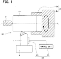
- an abnormality determining device which determines an abnormal heat generation (state) of a cutting device through use of a state detection sensor of the present disclosure.
- the cutting device S1 includes a blade 1 and a pair of first and second jigs 2, 3.
- the blade 1 is fixed to a support member 4.
- the first jig 2 includes a main body 2a and three holding portions 2b (only two of the holding portions 2b are shown in FIG. 1 ), which project from the main body 2a in a common direction.
- a processing subject member 10 is clamped with the three holding portions 2b.
- the second jig 3 is placed on an opposite side of the processing subject member 10, which is opposite from the side where the processing subject member 10 is clamped by the first jig 2, such that the second jig 3 cooperates with the first jig 2 to fix the processing subject member 10.
- the processing subject member 10 is fixed with the first and second jigs 2, 3, and the processing subject member 10 is rotated together with the first and second jigs 2, 3 about an axial direction L that is parallel with the projecting direction of the holding portions 2b of the first jig 2 and extends through a center of the main body 2a, and at the same time, the processing subject member 10 is brought into contact with the blade 1 to cut the processing subject member 10 with the blade 1.
- the abnormality determining device S2 includes a state detection sensor (state detection device) 20 and a control unit (control device) 30.
- the state detection sensor 20 is installed to the blade 1.
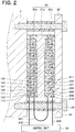
- the state detection sensor 20 includes first and second heat flux sensors 20a, 20b, a thermal buffer body 21 a and a heat releasing body 22.
- first and second heat flux sensors 20a, 20b First of all, the structure of the first and second heat flux sensors 20a, 20b will be described with reference to FIGS. 3 to 5 .
- the first and second heat flux sensors 20a, 20b have an identical structure. Therefore, only the structure of the first heat flux sensor 20a will be described as an example. However, each reference sign in parentheses in FIGS. 3 to 5 corresponds to a corresponding reference sign of the second heat flux sensor 20b.
- a dielectric substrate 100, a front surface protective member 110 and a back surface protective member 120 are formed integrally into a one-piece body, and primary and secondary interlayer connecting members 130, 140 are alternately connected in series in an inside of this integrated one-piece body.
- the front surface protective member 110 is omitted for the sake of easy understanding.
- the dielectric substrate 100 is a planar rectangular film made of thermoplastic resin, such as poly ether ether ketone (PEEK), poly ether imide (PEI), or liquid crystal polymer (LCP).
- a plurality of primary via holes 101 and a plurality of secondary via holes 102 extend through the dielectric substrate 100 in a thickness direction of the dielectric substrate 100, which is perpendicular to a plane of the dielectric substrate 100.
- the primary via holes 101 and the secondary via holes 102 are arranged in a hound's-tooth check pattern such that the primary via holes 101 and the secondary via holes 102 are alternately arranged one after another.
- Each of the primary and secondary via holes 101, 102 is shaped into a cylindrical form that has a constant diameter from a front surface 100a to a back surface 100b of the dielectric substrate 100.
- each of the primary and secondary via holes 101, 102 may be shaped into a tapered form that has a progressively decreasing diameter from the front surface 100a to the back surface 100b.
- each of the primary and secondary via holes 101, 102 may be shaped into a tapered form that has a progressively decreasing diameter from the back surface 100b toward the front surface 100a.
- each of the primary and secondary via holes 101, 102 may be shaped into a square tube form.
- Each of the primary interlayer connecting members 130 is placed in an inside of a corresponding one of the primary via holes 101, and each of the secondary interlayer connecting members 140 is placed in an inside of a corresponding one of the secondary via holes 102. That is, the primary interlayer connecting members 130 and the secondary interlayer connecting members 140 are alternately arranged one after another in the dielectric substrate 100.
- Each primary interlayer connecting member 130 and each secondary interlayer connecting member 140 are made of different types of electrically conductive metals, so that a Seebeck effect is exerted therebetween.
- the primary interlayer connecting member 130 is made of an intermetallic compound (sintered alloy) that is formed by solid-state sintering of P-type Bi-Sb-Te alloy powder that is sintered in such a manner that a crystalline structure of metal atoms before the solid-state sintering is maintained after the solid-state sintering.
- the secondary interlayer connecting member 140 is made of an intermetallic compound that is formed by solid-state sintering of N-type Bi-Te alloy powder that is sintered in such a manner that a crystalline structure of metal atoms before the sintering is maintained after the solid-state sintering.
- an electromotive voltage can be increased.
- FIG. 3 is not a cross sectional view, a hatching is applied to the primary and secondary interlayer connecting members 130, 140 to ease understanding.
- a front surface protective member 110 is placed on the front surface 100a of the dielectric substrate 100.
- the front surface protective member 110 is a planar rectangular film made of thermoplastic resin, such as poly ether ether ketone (PEEK), poly ether imide (PEI), or liquid crystal polymer (LCP).
- the planar form of the front surface protective member 110 has the same size as the planar form of the dielectric substrate 100.
- Patterning of, for example, copper foil is applied to one surface 110a of the front surface protective member 110, which is opposed to the dielectric substrate 100, so that a plurality of front surface patterns (a plurality of front surface conductor portions) 111, which have electrical conductivity, is formed on the one surface 110a such that the front surface patterns 111 are spaced from each other.
- Each corresponding one of the front surface patterns 111 is electrically connected to the corresponding primary and secondary interlayer connecting members 130, 140.
- each of the primary interlayer connecting members 130 and an adjacent one of the secondary interlayer connecting members 140, which is adjacent to this primary interlayer connecting member 130 form a set 150.
- the primary interlayer connecting member 130 and the secondary interlayer connecting member 140 of each set 150 are joined to a corresponding common one of the front surface patterns 111. That is, the primary and secondary interlayer connecting members 130, 140 of each set 150 are electrically connected to each other through the common front surface pattern 111.
- the corresponding primary interlayer connecting member 130 and the corresponding secondary interlayer connecting member 140 which are adjacent to each other in a longitudinal direction of the dielectric substrate 100 (a left-to-right direction in FIG. 4 ), form the set 150.
- a back surface protective member 120 is placed on the back surface 100b of the dielectric substrate 100.
- the back surface protective member 120 is a planar rectangular film made of thermoplastic resin, such as poly ether ether ketone (PEEK), poly ether imide (PEI), or liquid crystal polymer (LCP).
- the planar form of the back surface protective member 120 has the same size as the planar form of the dielectric substrate 100.
- Patterning of, for example, copper foil is applied to one surface 120a of the back surface protective member 120, which is opposed to the dielectric substrate 100, so that a plurality of back surface patterns (a plurality of back surface conductor portions) 121, which have electrical conductivity, is formed on the one surface 120a such that the back surface patterns 121 are spaced from each other.
- Each corresponding one of the back surface patterns 121 is electrically connected to the corresponding primary and secondary interlayer connecting members 130, 140.
- the primary interlayer connecting member 130 of one of the adjacent sets 150 and the secondary interlayer connecting member 140 of another one of the adjacent sets 150 are joined to a corresponding common one of the back surface patterns 121. That is, the primary interlayer connecting member 130 of the one set 150 and the secondary interlayer connecting member 140 of the other set 150 are electrically connected to each other through the common back surface pattern 121.
- each corresponding primary interlayer connecting member 130 and the corresponding secondary interlayer connecting member 140 which are adjacent to each other in a direction (a top-to-bottom direction in FIG. 3 ) that is perpendicular to the longitudinal direction, are joined to the corresponding common back surface pattern 121.
- the adjacent primary and secondary interlayer connecting members 130, 140 are joined to the common back surface pattern 121 at the outer edge of the dielectric substrate 100 such that a row of the primary and secondary interlayer connecting members 130, 140, which are connected in series by the corresponding front surface patterns 111 and the corresponding back surface patterns 121 in the longitudinal direction of the dielectric substrate 100, are turned at the outer edge of the dielectric substrate 100 to form another row of the primary and secondary interlayer connecting members 130, 140, which are connected in series by the front surface patterns 111 and the back surface patterns 121 in the longitudinal direction of the dielectric substrate 100, and so on.
- the basic structure of the first heat flux sensor 20a of the present embodiment has been described. As discussed above, the structure of the second heat flux sensor 20b is similar to the structure of the first heat flux sensor 20a.
- a dielectric substrate 200, a front surface protective member 210 and a back surface protective member 220 are formed integrally into a one-piece body.
- Each of primary and secondary via holes 201, 202 is shaped into a cylindrical form that has a constant diameter from a front surface 200a to a back surface 200b of the dielectric substrate 200.
- Each of primary interlayer connecting members 230 is placed in an inside of a corresponding one of the primary via holes 201, and each of the secondary interlayer connecting members 240 is placed in an inside of a corresponding one of the secondary via holes 202.
- the planar form of the front surface protective member 210 has the same size as the planar form of the dielectric substrate 200.
- Patterning of, for example, copper foil is applied to one surface 210a of the front surface protective member 210, which is opposed to the dielectric substrate 200, so that a plurality of front surface patterns 211 is formed on the one surface 210a such that the front surface patterns 211 are spaced from each other.
- Each of the front surface patterns 211 is electrically connected to the corresponding first and second interlayer connecting members 230, 240.
- the planar form of the back surface protective member 220 has the same size as the planar form of the dielectric substrate 200.
- Patterning of, for example, copper foil is applied to one surface 220a of the back surface protective member 220, which is opposed to the dielectric substrate 200, so that a plurality of back surface patterns 221 is formed on the one surface 220a such that the back surface patterns 221 are spaced from each other.
- Each of the back surface patterns 221 is electrically connected to the corresponding first and second interlayer connecting members 230, 240.
- each of the primary interlayer connecting members 230 and an adjacent one of the secondary interlayer connecting members 240 which is adjacent to this primary interlayer connecting member 230, form a set 250.
- the primary interlayer connecting member 230 and the secondary interlayer connecting member 240 of each set 250 are joined to a corresponding common one of the front surface patterns 211.
- the first and second heat flux sensors 20a, 20b which are constructed in the above-described manner, outputs a sensor signal (electromotive voltage), which corresponds to a heat flux that passes through the first and second heat flux sensors 20a, 20b in a thickness direction of the respective first and second heat flux sensors 20a, 20b.
- a sensor signal electrotive voltage
- the thickness direction of each of the first and second heat flux sensors 20a, 20b is a stacking direction of the dielectric substrate 100, the front surface protective member 110 and the back surface protective member 120 and is perpendicular to a plane of the dielectric substrate 100.
- the manufacturing method of the second heat flux sensor 20b is similar to the manufacturing method of the first heat flux sensor 20a.
- the dielectric substrate 100 is prepared, and the primary via holes 101 are formed in the dielectric substrate 100 through use of, for example, a drill or a laser light.
- primary conductive paste 131 is filled into the respective primary via holes 101.
- a method (device) for filling the primary conductive paste 131 into the primary via holes 101 a method (device) disclosed in Japanese patent application number 2010-50356 ( JP2011-187619A ), which is filed by the applicant of the present application, may be used.
- the dielectric substrate 100 is placed on a holder (not shown) through an adsorption paper 160 in such a manner that the back surface 100b is opposed to the adsorption paper 160. Then, the primary conductive paste 131, which is melted, is filled into the respective primary via holes 101. Thereby, a majority of organic solvent of the primary conductive paste 131 is adsorbed by the adsorption paper 160, so that the alloy powder is cohesively held in the respective primary via holes 101.
- the adsorption paper 160 can be any paper that can adsorb the organic solvent of the primary conductive paste 131.
- a typical woodfree paper may be used as the adsorption paper 160.
- the primary conductive paste 131 is prepared as follows. That is, the Bi-Sb-Te alloy powder, in which the metal atoms maintain the predetermined crystalline structure, is added into the organic solvent, such as paraffin, which has the melting point of 43 degrees Celsius, to form the paste that is used as the primary conductive paste 131.
- the front surface 100a of the dielectric substrate 100 is heated to about 43 degrees Celsius.
- the secondary via holes 102 are formed in the dielectric substrate 100 through use of, for example, a drill or a laser light. As discussed above, the secondary via holes 102 and the primary via holes 101 are alternately arranged to form the hound's-tooth check pattern.
- secondary conductive paste 141 is filled into the respective secondary via holes 102. This step can be executed in a manner similar to that of the step of FIG. 6(b) .
- the dielectric substrate 100 is placed on the holder (not shown) through the adsorption paper 160 in such a manner that the back surface 100b is opposed to the adsorption paper 160. Then, the secondary conductive paste 141 is filled into the secondary via holes 102. Thereby, a majority of organic solvent of the secondary conductive paste 141 is adsorbed by the adsorption paper 160, so that the alloy powder is cohesively held in the respective secondary via holes 102.
- the secondary conductive paste 141 is prepared as follows. That is, the Bi-Te alloy powder, in which the metal atoms maintain the predetermined crystalline structure that is different from that of the metal atoms of the primary conductive paste 131, is added into the organic solvent, such as terpene, which has the melting point of the room temperature, to form the paste that is used as the secondary conductive paste 141.
- the organic solvent which is used in the secondary conductive paste 141, has the melting temperature that is lower than the melting point of the organic solvent, which is used in the primary conductive paste 131.
- the front surface 100a of the dielectric substrate 100 is kept at the room temperature. In other words, the filling of the secondary conductive paste 141 is executed in a solidified state of the organic solvent, which is contained in the primary conductive paste 131. Thereby, intrusion of the secondary conductive paste 141 into the primary via holes 101 is limited.
- the solidified state of the organic solvent which is contained in the primary conductive paste 131, refers to the state of the organic solvent left in the primary via hole 101 without being adsorbed by the adsorption paper 160 at the step shown in FIG. 6(b) .
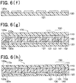
- the copper foil or the like is formed on the one surface 110a of the front surface protective member 110 and the one surface 120a of the back surface protective member 120, which are opposed to the dielectric substrate 100, as shown in FIGS. 6(e) and 6(f) .
- the copper foil By appropriately pattering the copper foil, there are prepared the front surface protective member 110 that has the front surface patterns 111, which are spaced from each other, as well as the back surface protective member 120 that has the back surface patterns 121, which are spaced from each other.
- the back surface protective member 120, the dielectric substrate 100 and the front surface protective member 110 are sequentially stacked one after another to form a laminated body 170.
- this laminated body 170 is placed between a pair of press plates. Then, the laminated body 170 is heated and pressed between the press plates from the upper side and the lower side in the stacking direction in a vacuum state, so that the laminated body 170 is formed integrally into a one-piece body. Specifically, the laminated body 170 is formed integrally into the one-piece body through the heating and pressurization, which are executed in such a manner that the primary and secondary conductive pastes 131, 141 are solid-state sintered to form the primary and secondary interlayer connecting members 130, 140, and the primary and secondary interlayer connecting members 130, 140 are joined to the front surface pattern 111 and the back surface pattern 121.
- a cushioning material such as a rockwool paper, may be placed between the laminated body 170 and the respective press plates at the time of integrally forming the laminated body 170 into the one-piece body.
- the first heat flux sensor 20a is manufactured in the above-described manner.
- a thermal buffer body (thermal storage body) 21 a which is a heat conductor, is in a form of a planar plate that has a predetermined heat capacity (thermal resistance) and is made of, for example, metal (e.g., Cu or Al) or resin.
- the planar form of the thermal buffer body 21a has the same size as that of the first and second heat flux sensors 20a, 20b, the size of the planar form of the thermal buffer body 21 a may be different from that of the first and second heat flux sensors 20a, 20b.
- the thermal buffer body 21 a is a one-piece metal plate that is made of metal (e.g., Cu or Al) and extends continuously through an extent that is equal to or larger than a sensing range SE (see FIG. 3 ), which includes all of the primary interlayer connecting members 130 and the secondary interlayer connecting members 240 formed in the dielectric substrate 100 of the first heat flux sensor 20a, in a plane that is parallel to a plane of the dielectric substrate 100 of the first heat flux sensor 20a and a plane of the dielectric substrate 200 of the second heat flux sensor 20b.
- a sensing range SE see FIG. 3
- the heat releasing body 22 is in a form of a planar plate that has a predetermined heat capacity (thermal resistance) and is made of, for example, metal (e.g., Cu or Al) or resin.
- the material, the thickness and the like of the heat releasing body 22 are appropriately adjusted, so that the heat capacity of the heat releasing body 22 becomes larger than the heat capacity of the thermal buffer body 21a.
- the size of the planar form of the heat releasing body 22 is larger than the size of the planar form of the first and second heat flux sensors 20a, 20b and the thermal buffer body 21 a.
- the heat releasing body 22 directly releases the heat to the surrounding atmosphere.
- the heat releasing body 22 may release the heat to another heat sink or coolant.
- the state detection sensor 20 is installed to the blade 1 in such a manner that the first heat flux sensor 20a, the thermal buffer body 21 a, the second heat flux sensor 20b and the heat releasing body 22 are arranged one after another in this order from the blade 1 side. That is, the thermal buffer body 21 a is interposed between the first heat flux sensor 20a and the second heat flux sensor 20b.
- the blade 1 corresponds to the sensing subject of the present disclosure.
- the state detection sensor 20 When the state detection sensor 20 is viewed in an array direction (stacking direction) of the first heat flux sensor 20a, the thermal buffer body 21 a, the second heat flux sensor 20b and the heat releasing body 22, projecting portions of the heat releasing body 22, which project from the second heat flux sensor 20b, are fixed to the blade 1 with screws 23, and thereby the state detection sensor 20 is fixed to the blade 1.
- Each of the screws 23 is received through a corresponding one of the spacers 24 and is securely screwed to the blade 1.
- an adhesive heat transfer member such as a heat transfer sheet or heat transfer paste, is interposed between each adjacent two of the first heat flux sensor 20a, the thermal buffer body 21 a, the second heat flux sensor 20b and the heat releasing body 22, so that each adjacent two of the first heat flux sensor 20a, the thermal buffer body 21 a, the second heat flux sensor 20b and the heat releasing body 22 are bonded together through the adhesive heat transfer member.
- the first and second heat flux sensors 20a, 20b are arranged such that when the heat flux is generated between the blade 1 and the heat releasing body 22 (the atmosphere), the polarity of the voltage of the first sensor signal, which is outputted from the first heat flux sensor 20a, is opposite from the polarity of the voltage of the second sensor signal, which is outputted from the second heat flux sensor 20b. That is, the first and second heat flux sensors 20a, 20b are arranged such that for example, in a case where the polarity of the voltage of the first sensor signal is positive, the polarity of the voltage of the second sensor signal is negative.
- the first and second heat flux sensors 20a, 20b are arranged such that the front surface protective members 110 of the first and second heat flux sensors 20a, 20b are opposed to each other. Furthermore, an external wiring 302 connects a corresponding one of the back surface patterns 121, which is provided to an output terminal 601 a (see FIG. 3 ) of the first heat flux sensor 20a, to a control unit 30. An external wiring 301 connects a corresponding one of the front surface patterns 111, which is provided to a connection terminal 601b (see FIG.
- an external wiring 303 connects a corresponding one of the back surface patterns 221, which is provided to an output terminal 701 a of the second heat flux sensor 20b that is opposite from the connection terminal 701 b of the second heat flux sensor 20b to the control unit 30.
- the external wiring 301 extends downward in FIG. 2
- the external wiring 301 may extend upward in FIG. 2 .
- the first and second heat flux sensors 20a, 20b are opposed to each other in the above-described manner, so that in a case where the heat flux passes through the first heat flux sensor 20a from the back surface protective member 120 side to the front surface protective member 110 side, this heat flux passes through the second heat flux sensor 20b from the front surface protective member 210 side to the back surface protective member 220 side. Thereby, the polarity of the first sensor signal outputted from the first heat flux sensor 20a and the polarity of the second sensor signal outputted from the second heat flux sensor 20b become opposite to each other.
- the first and second heat flux sensors 20a, 20b are arranged such that when a heat flux, which flows from the back surface protective member 120, 220 side to the front surface protective member 110, 210 side, passes through the first or second heat flux sensor 20a, 20b, the first or second heat flux sensor 20a, 20b outputs the sensor signal that has the positive voltage.
- the heat flux which flows from the blade 1 toward the heat releasing body 22
- the heat flux which passes through the first heat flux sensor 20a from the back surface protective member 120 side to the front surface protective member 110 side and passes through the second heat flux sensor 20b from the front surface protective member 210 side to the back surface protective member 220 side
- the sensor signal of the positive voltage is outputted from the first heat flux sensor 20a
- the sensor signal of the negative voltage is outputted from the second heat flux sensor 20b.
- the control unit 30 includes a CPU, various types of memories which form a storage device (storage means), and a peripheral device(s).
- the control unit 30 is connected to, for example, a speaker (speech means) and/or a display device (display means), which are not shown.
- the control unit 30 is connected to the first and second heat flux sensors 20a, 20b in the above-described manner.
- the control unit 30 determines whether abnormal heating is generated at the blade 1 based on the first and second sensor signals and a threshold value stored in the storage means.
- the control unit 30 determines whether the abnormal heating is generated at the blade 1 by comparing a sum of the first and second sensor signals with the threshold value. When the control unit 30 determines that the abnormal heating is generated at the blade 1, the control unit 30 notifies the generation of the abnormal heating at the blade 1 to a worker through the display device (display means) and/or the speaker (speech means). The abnormal heating is generated at the blade 1 in a case of, for example, occurrence of chipping of the blade 1.
- the structure of the abnormality determining device S2 of the present embodiment has been described. Next, an abnormality determining method through use of the abnormality determining device S2 will be described. First of all, the heat flux, which passes through the first and second heat flux sensors 20a, 20b, and the first and second sensor signals, which are outputted from the first and second heat flux sensors 20a, 20b, will be described.
- the heat releasing body 22 is exposed to the surrounding atmosphere, the heat releasing body 22 is formed to have the predetermined heat capacity, as discussed above.
- the heat releasing body 22 accumulates heat and release the heat in response to the change in the temperature of the surrounding atmosphere. Therefore, influence of the surrounding atmosphere to the first and second heat flux sensors 20a, 20b, which is located on the blade 1 side of the heat releasing body 22, is limited.
- the thermal buffer body 21 a is in a state where a predetermined amount of heat is accumulated in the thermal buffer body 21a.
- the heat flux, which passes through the first heat flux sensor 20a is generally equal to the heat flux, which passes through the second heat flux sensor 20b. Therefore, the voltage of the first sensor signal outputted from the first heat flux sensor 20a and the voltage of the second sensor signal outputted from the second heat flux sensor 20b have generally the identical absolute value but opposite polarities, respectively. Therefore, in this state, a sum of the voltage of the first sensor signal and the voltage of the second sensor signal is generally 0 (zero).
- the heat flux, which passes through the first heat flux sensor 20a does not substantially change, as indicated by arrows in FIG. 7B . That is, the heat flux, which passes through the first heat flux sensor 20a, differs from the heat flux, which passes through the second heat flux sensor 20b.
- the voltage of the first sensor signal outputted from the first heat flux sensor 20a and the voltage of the second sensor signal outputted from the second heat flux sensor 20b have different absolute values and opposite polarities. That is, in the case where the abnormal heating is generated at the blade 1, the first and second sensor signals, which correspond to the abnormal heating, are outputted from the first and second heat flux sensors 20a, 20b regardless of the state of the surrounding atmosphere.
- FIG. 8 is a diagram indicating a relationship between the sum of the voltage of the first sensor signal and the voltage of the second sensor signal and the time in a case where the abnormal heating is generated at the blade 1 at a time point T1.
- the control unit 30 determines whether the abnormal heating is generated at the blade 1 based on the sum of the voltage of the first sensor signal and the voltage of the second sensor signal and also based on the threshold value. In the present embodiment, the control unit 30 determines whether the sum of the voltage of the first sensor signal and the voltage of the second sensor signal is larger than the threshold value. In a case where the control unit 30 determines that the sum of the voltage of the first sensor signal and the voltage of the second sensor signal is larger than the threshold value, the control unit 30 determines that the abnormal heating is generated at the blade 1 (the cutting device S1).
- the control unit 30 determines that the blade 1 is normal.
- the control unit 30 determines that the abnormal heating is generated at the blade 1 and notifies the generation of the abnormal heating at the blade 1 to the worker through, for example, the speech means and/or the display means.
- the heat of the abnormal heating is accumulated in the thermal buffer body 21a. Therefore, the difference between the heat flux, which passes through the first heat flux sensor 20a, and the heat flux, which passes through the second heat flux sensor 20b, is progressively reduced. Therefore, after the time point T3, the sum of the voltage of the first sensor signal and the voltage of the second sensor signal approaches 0 (zero).
- the state detection sensor 20 of the present embodiment includes: the first and second heat flux sensors 20a, 20b, which respectively output the first and second sensor signals that correspond to the heat flux passing through the first and second heat flux sensors 20a, 20b in the thickness direction; the thermal buffer body 21a, which has the predetermined heat capacity; and the heat releasing body 22, which has the predetermined heat capacity. Furthermore, the first heat flux sensor 20a, the thermal buffer body 21 a, the second heat flux sensor 20b and the heat releasing body 22 are arranged in this order from the blade 1 side. Therefore, since the heat releasing body 22 executes the releasing and accumulating of the heat, it is possible to limit the influence of the surrounding atmosphere on the first and second heat flux sensors 20a, 20b.
- the thermal buffer body 21 a between the first heat flux sensor 20a and the second heat flux sensor 20b, in the case where the abnormal heating is not generated at the blade 1, the heat flux, which passes through the first heat flux sensor 20a, and the heat flux, which passes through the second heat flux sensor 20b, become equal to each other (see FIG. 7A ). Furthermore, in the case where the abnormal heating is generated at the blade 1, the heat flux, which passes through the first heat flux sensor 20a, and the heat flux, which passes through the second heat flux sensor 20b, momentarily become different from each other (see FIG. 7B ). Thus, it is possible to limit deterioration of the sensing accuracy for sensing the state of the blade 1 regardless of the state of the surrounding atmosphere.
- the state detection sensor 20 can output the accurate first and second sensor signals regardless of the state of the surrounding atmosphere. Therefore, the determining accuracy for the abnormal heating at the blade 1 can be improved.
- the first heat flux sensor 20a and the second heat flux sensor 20b are arranged such that the polarity of the voltage of the first sensor signal outputted from the first heat flux sensor 20a and the polarity of the voltage of the second sensor signal outputted from the second heat flux sensor 20b are opposite to each other. Therefore, the computing process at the control unit 30 can be simplified.
- the first and second heat flux sensors 20a, 20b are formed such that the primary and secondary via holes 101, 102 are formed in the dielectric substrate 100 made of the thermoplastic resin, and the primary and secondary interlayer connecting members 130, 140 are placed in the primary and secondary via holes 101, 102. Therefore, by appropriately changing, for example, the numbers, the diameters, and the intervals of the primary and secondary via holes 101, 102, it is possible to increase the density of the primary and secondary interlayer connecting members 130, 140. Thereby, the electromotive voltage can be increased to improve the sensitivity of the first and second heat flux sensors 20a, 20b.
- the first and second heat flux sensors 20a, 20b use the intermetallic compounds (the Bi-Sb-Te alloy, the Bi-Te alloy) as the primary and secondary interlayer connecting members 130, 140, and these intermetallic compounds (the Bi-Sb-Te alloy, the Bi-Te alloy) are solid-state sintered such that the crystalline structure before the execution of the solid-state sintering is maintained upon the execution of the solid-state sintering. That is, the metals of the primary and secondary interlayer connecting members 130, 140, 230, 240 are the sintered metals, which are sintered in the state where the metal atoms thereof maintain the crystalline structure thereof.
- the electromotive voltage can be increased, and thereby the sensitivity of the first and second heat flux sensors 20a, 20b can be increased.
- the dielectric substrates 100, 200, the front surface protective members 110, 210, and the back surface protective member 120, 220 are made of the thermoplastic resin and have the flexibility. Therefore, the shapes of the first and second heat flux sensors 20a, 20b can be appropriately changed according to the shape of the place where the first and second heat flux sensors 20a, 20b are installed.
- the abnormality is determined by determining whether the sum of the voltage of the first sensor signal and the voltage of the second sensor signal is larger than the threshold value.
- the abnormality may be determined based on the time period (the time period from the time point T2 to the time point T4 in FIG. 8 ), in which the sum of the voltage of the first sensor signal and the voltage of the second sensor signal is larger than the threshold value. In this way, it is possible to eliminate the case where the sum of the voltage of the first sensor signal and the voltage of the second sensor signal is momentarily increased above the threshold value due to, for example, a noise. Thus, the determining accuracy can be further improved.
- a second embodiment of the present disclosure will be described.
- a heat receiving body is placed on an opposite side of the first heat flux sensor 20a, which is opposite from the thermal buffer body 21a.
- the rest of the present embodiment is the same as that of the first embodiment and thereby will not be described for the sake of simplicity.
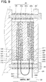
- the state detection sensor 20 includes the heat receiving body 25, which is placed on the opposite side of the first heat flux sensor 20a, which is opposite from the thermal buffer body 21a. That is, the state detection sensor 20 includes the heat receiving body 25, which is placed between the blade 1 and the first heat flux sensor 20a.
- the heat receiving body 25 is in a form of a planar plate that has a predetermined heat capacity (thermal resistance) and is made of, for example, metal (e.g., Cu or Al) or resin.
- the material and the thickness of the heat receiving body 25 of the present embodiment are adjusted such that the heat capacity of the heat receiving body 25 is smaller than the heat capacity of the thermal buffer body 21 a and the heat capacity of the heat releasing body 22.
- the state detection sensor 20 constructed in the above-described manner, it is possible to limit occurrence of that the first and second heat flux sensors 20a, 20b are influenced by a small heat flux change, such as a noise, which is generated at the blade 1 through the releasing and accumulating of the heat at the heat receiving body 25. Therefore, the state sensing accuracy can be further improved.
- a third embodiment of the present disclosure will be described.
- additional heat flux sensors and additional thermal buffer bodies are provided to the structure of the first embodiment.
- the rest of the present embodiment is the same as that of the first embodiment and thereby will not be described for the sake of simplicity.
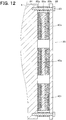
- the state detection sensor 20 includes third and fourth heat flux sensors 20c, 20d and thermal buffer bodies 21 b, 21 c in addition to the first and second heat flux sensors 20a, 20b and the thermal buffer body 21 a.
- the first heat flux sensor 20a, the thermal buffer body 21 a, the second heat flux sensor 20b, the thermal buffer body 21 b, the third heat flux sensor 20c, the thermal buffer body 21 c, the fourth heat flux sensor 20d and the heat releasing body 22 are arranged one after another in this order from the blade 1 side.
- the constructions of the third and fourth heat flux sensors 20c, 20d are the same as the constructions of the first and second heat flux sensors 20a, 20b.
- the third and fourth heat flux sensors 20c, 20d respectively output third and fourth sensor signals, which correspond to the heat flux that passes the third and fourth heat flux sensors 20c, 20d in the thickness direction thereof.
- FIG. 1 In FIG. 1
- the references signs of the dielectric substrate 100, the front surface protective member 110, the front surface patterns 111, the back surface protective member 120, the back surface patterns 121 and the primary and secondary interlayer connecting members 130, 140 of the third heat flux sensor 20c are the same as those of the first heat flux sensor 20a
- the reference signs of the dielectric substrate 200, the front surface protective member 210, the front surface patterns 211, the back surface protective member 220, the back surface patterns 221 and the first and second interlayer connecting members 230, 240 are the same as those of the second heat flux sensor 20b.
- the third and fourth heat flux sensors 20c, 20d are arranged such that the front surface protective member 110 of the third heat flux sensor 20c and the front surface protective member 210 of the fourth heat flux sensor 20d are opposed to each other. Furthermore, an external wiring 304 connects a corresponding one of the back surface patterns 121, which is provided to the output terminal 601 a (see FIG. 3 ) of the third heat flux sensor 20c, to the control unit 30. An external wiring 305 connects a corresponding one of the front surface patterns 111, which is provided to the connection terminal 601b (see FIG.
- an external wiring 306 connects a corresponding one of the back surface patterns 221, which is provided to the output terminal 701 a of the fourth heat flux sensor 20d that is opposite from the connection terminal 701 b of the fourth heat flux sensor 20d, to the control unit 30.
- the third and fourth heat flux sensors 20c, 20d are opposed to each other in the above-described manner.
- the thermal buffer bodies 21 b, 21c are in a form of a planar plate that has a predetermined heat capacity (thermal resistance) and is made of, for example, metal (e.g., Cu or Al) or resin.
- the thermal buffer bodies 21a-21c are constructed to have the identical heat capacity.
- the thermal buffer bodies 21a-21c are respectively provided as a first thermal buffer body (first thermal storage body), a second thermal buffer body (second thermal storage body), and a third thermal buffer body (third thermal storage body).
- the control unit 30 receives the third and fourth sensor signals in addition to the first and second sensor signals.
- the control unit 30 adds up a sum of the voltages of the first and second sensor signals and a sum of the voltages of the third and fourth sensor signals together. Then, the control unit 30 compares this added value with a corresponding threshold value to determine whether abnormal heating is generated at the blade 1.
- the state detection sensor 20 which is constructed in the above-described manner, in the case where the abnormal heating is not generated in the blade 1, or after elapse of the predetermined time period from the time of generating the abnormal heating at the blade 1, the respective thermal buffer bodies 21 a-21 c are in a state where a predetermined amount of heat is accumulated in the thermal buffer body 21a-21c.
- the heat fluxes which respectively pass through the first to fourth heat flux sensors 20a-20d, become generally equal to each other. Therefore, the voltage of the first sensor signal and the voltage of the second sensor signal have generally the identical absolute value but opposite polarities, respectively, and the voltage of the third sensor signal and the voltage of the fourth sensor signal have generally the identical absolute value but opposite polarities, respectively.
- the heat of the abnormal heating is sequentially accumulated in the thermal buffer bodies 21a-21c.
- the heat flux, which passes through the first heat flux sensor 20a is increased first, and then the heat flux, which passes through the second heat flux sensor 20b, the heat flux, which passes through the third heat flux sensor 20c, and the heat flux, which passes through the fourth heat flux sensor 20d, are sequentially increased.
- the heat fluxes, which respectively pass through the first to fourth heat flux sensors 20a-20d become generally equal to each other.
- the voltage of the first sensor signal and the voltage of the second sensor signal have different polarities and different absolute values.
- the voltage of the third sensor signal and the voltage of the fourth sensor signal have different polarities and different absolute values.
- FIG. 11 is a diagram that shows a relationship of the total value of the sum of the voltages of the first and second sensor signals and the sum of the voltages of the third and fourth sensor signals with time in the case where the abnormal heating is generated at the blade 1 at the time point T11.
- control unit 30 determines whether the abnormal heating is generated at the blade 1 based on the total value of the sum of the voltages of the first and second sensor signals and the sum of the voltages of the third and fourth sensor signals and also based on the threshold value.
- the heat fluxes which pass through the first to fourth heat flux sensors 20a-20d, are equal to each other before the time point T11, at which the abnormal heating is generated at the blade 1, so that the total value of the sum of the voltages of the first and second sensor signals and the sum of the voltages of the third and fourth sensor signals is lower than the threshold value.
- the control unit 30 determines that the blade 1 is normal.
- the heat flux, which passes through the first heat flux sensor 20a, and the heat flux, which passes through the second heat flux sensor 20b, are different from each other.
- the heat flux, which passes through the third heat flux sensor 20c, and the heat flux, which passes through the fourth heat flux sensor 20d are still equal to each other at the time immediately after the generation of abnormal heating at the time point T11. Since the heat flux, which passes through the first heat flux sensor 20a, and the heat flux, which passes through the second heat flux sensor 20b, are different from each other, the total value, which is obtained through the addition, becomes larger than the threshold value at the time point T12.
- the heat of the abnormal heating is also sequentially accumulated in the thermal buffer bodies 21 b, 21 c. That is, after the heat flux, which passes through the first heat flux sensor 20a, is increased, the heat flux, which passes through the second heat flux sensor 20b, the heat flux, which passes through the third heat flux sensor 20c, and the heat flux, which passes through the fourth heat flux sensor 20d, are sequentially increased. Specifically, a difference between the heat flux, which passes through the first heat flux sensor 20a, and the heat flux, which passes through the second heat flux sensor 20b, is reduced from the time point T13.
- the total value is increased once again from the time point T14.
- a difference between the heat flux, which passes through the third heat flux sensor 20c, and the heat flux, which passes through the fourth heat flux sensor 20d, is also reduced from the tie point T15.
- the total value becomes smaller than the threshold value at the tie point T16. That is, in the present embodiment, the total value becomes larger than the threshold value in the period that is from the time point T12 to the time point T16.
- the state detection sensor 20 may be constructed to have the first to fourth heat flux sensors 20a-20d and the thermal buffer bodies 21a-21c.
- the time period (the time point T12 to the time point T15), during which the total value is larger than the threshold value, is lengthened.
- the determining accuracy can be further improved.
- a fourth embodiment of the present disclosure will be described.
- a plurality of sets of the first and second heat flux sensors 20a, 20b is provided to the structure of the first embodiment.
- the rest of the present embodiment is the same as that of the first embodiment and thereby will not be described for the sake of simplicity.
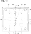
- the state detection sensor 20 has first to ninth arrangements 40a-40i, each of which includes the first heat flux sensor 20a, the thermal buffer body 21a, and the second heat flux sensor 20b.
- the first to ninth arrangements 40a-40i are arranged such that the first arrangement 40a is centered, and the second to ninth arrangements 40b-40i are evenly arranged around the first arrangement 40a.
- One piece of heat releasing body 22 is placed on the second heat flux sensor 20b having the first to ninth arrangements 40a-40i. That is, in the present embodiment, the heat releasing body 22 is common to the first to ninth arrangements 40a-40i.
- control unit 30 receives the first and second sensor signals from the first and second heat flux sensors 20a, 20b of each of the first to ninth arrangements 40a-40i. Every sum of the voltage of the first sensor signal and the voltage of the second sensor signal at each of the first to ninth arrangements 40a-40i is added together to obtain a total value, and this total value is compared with a threshold value to determine whether the abnormal heating is generated at the blade 1.
- the first and second sensor signals which are similar to those of the first embodiment, are outputted from the first and second heat flux sensors 20a, 20b at each of the first to ninth arrangements 40a-40i.
- the control unit 30 adds every sum of the voltage of the first sensor signal and the voltage of the second sensor signal generated at each of the first to ninth arrangements 40a-40i to obtain the total value, and then the control unit 30 compares this total value with the threshold value to determine whether the abnormal heating is generated at the blade 1.
- the control unit 30 determines that the blade 1 is normal.
- the control unit 30 determines that the abnormal heating is generated at the blade 1.
- the state detection sensor 20 may be constructed to have the first to ninth arrangements 40a-40i.
- the value (the total value), which is compared with the threshold value, becomes large. Therefore, the threshold value itself can be increased.
- the determining accuracy can be further improved.
- the heat releasing body 22 is common to the first to ninth arrangements 40a-40i.
- the first to ninth arrangements 40a-40i may have the heat releasing bodies 22, respectively.
- the number of the arrangements 40a-40i may be appropriately changed.
- a fifth embodiment of the present disclosure will be described.
- the structure of the state detection sensor 20 is changed from that of the first embodiment.
- the rest of the present embodiment is the same as that of the first embodiment and thereby will not be described for the sake of simplicity.
- the first and second heat flux sensors 20a, 20b are formed integrally into a one-piece body. That is, a single heat flux sensor is bent to clamp the thermal buffer body 21a.
- the first and second heat flux sensors 20a, 20b are connected with each other such that the front surface pattern 111, which is formed at the connection terminal 601b (see FIG. 3 ) of the first heat flux sensor 20a, and the front surface pattern 211, which is formed at the connection terminal 701 b (see FIG. 3 ) of the second heat flux sensor 20b, are directly and continuously connected with each other through a front surface pattern 350, which is formed at the front surface protective members 110, 210, without using the external wiring 301.
- the first and second heat flux sensors 20a, 20b are formed by the single heat flux sensor, and thereby the external wiring 301, which connects between the first heat flux sensor 20a and the second heat flux sensor 20b, can be eliminated.
- the number of components can be reduced.
- the manufacturing process will not be complicated. Furthermore, in the first and second heat flux sensors 20a, 20b, the dielectric substrates 100, 200, the front surface protective members 110, 210, and the back surface protective members 120, 220 are respectively made of the resin, so that the first and second heat flux sensors 20a, 20b can be easily bent.
- a sixth embodiment of the present disclosure will be described.
- abnormality determination of a milling device is executed.
- the rest of the present embodiment is the same as that of the first embodiment and thereby will not be described for the sake of simplicity.
- the milling device S3 includes a spindle 401, bearings 402, a support member 403, and an end mill 404.
- the spindle 401 rotates about an axis.
- the bearings 402 rotatably support the spindle 401.
- the support member 403 supports the spindle 401 and the bearings 402.
- the end mill 404 is installed to one end portion of the spindle 401 in the axial direction and includes blades 404a at an outer peripheral surface of the end mill 404.
- the end mill 404 is rotated synchronously with the spindle 401.
- the processing subject member 10 is cut with the blades 404a of the end mill 404 when the blades 404a are rotated and are urged against the processing subject member 10.
- the state detection sensors 20 are placed adjacent to the bearings 402, respectively, at the support member 403 in the milling device S3.
- the number of the bearings 402 is two, and each of the state detection sensors 20 is placed adjacent to the corresponding one of the bearings 402.
- the support member 403 corresponds to the sensing subject of the present disclosure. Furthermore, in the state detection sensor 20, although not particularly depicted, the first heat flux sensor 20a, the thermal buffer body 21a, the second heat flux sensor 20b and the heat releasing body 22 are arranged one after another in this order from the side where the support member 403 is placed. Specifically, these components are arranged such that the support member 403 is placed at the location of the blade 1 in FIG. 2 . In FIG. 15 , although the control unit 30 is not particularly indicated, the control unit 30 is configured to receive the first and second sensor signals from the first and second heat flux sensors 20a, 20b of the state detection sensor 20, like in the first embodiment.
- the abnormality determining method of the present embodiment will be described.
- the blades 404a of the end mill 404 are placed in contact with the processing subject member 10 to cut the processing subject member 10.
- the friction of the bearing 402 is rapidly increased.
- the abnormal heating is generated by the friction around the bearing 402. Therefore, as discussed with reference to FIGS. 7A and 7B , the heat flux, which passes through the first heat flux sensor 20a, and the heat flux, which passes through the second heat flux sensor 20b, momentarily become different from each other.
- control unit 30 determines whether the sum of the voltage of the first sensor signal and the voltage of the second sensor signal is larger than the threshold value. When it is the determined that the sum of the voltage of the first sensor signal and the voltage of the second sensor signal is larger than the threshold value, the control unit 30 determines that the abnormal heating is generated at the end mill 404 (the milling device S3).
- the abnormality determining device S2 which executes the abnormality determination of the milling device S3, can be formed with the state detection sensor 20 of the present disclosure, and the advantages, which are similar to those of the first embodiment, can be achieved.
- a seventh embodiment of the present disclosure will be described.
- abnormality determination of a transporting device is executed.
- the rest of the present embodiment is the same as that of the first embodiment and thereby will not be described for the sake of simplicity.
- the transporting device S4 includes a screw 501, support members 502 and a motor 503.
- the screw 501 includes a screw portion 501a.
- the support members 502 are installed to two axial end portions, respectively, of the screw 501.
- the motor 503 is installed to the support member 502.
- a nut 504 is paired with and is threadably installed to the screw 501 in such a manner that the nut 504 is movable in the axial direction of the screw 501.
- the nut 504 includes a bearing 504a and cooperates with the screw 501 to form a ball screw.
- the nut 504 is coupled to a pedestal 505.
- the pedestal 505 is provided to carry, for example, a device to be transported.
- the pedestal 505 is shaped into a planar rectangular form, and a longitudinal direction of this planar rectangular form extends in a direction (a top-to-bottom direction in FIG. 16 ) that is perpendicular to the axial direction of the screw 501.
- a generally center portion of the pedestal 505 is coupled to the nut 504.
- Two slide blocks 507 are installed to two longitudinal end portions, respectively, of the pedestal 505.
- the slide blocks 507 are engaged with rails 506 respectively and are movable along the rails 506.
- the support members 502 are omitted.
- the state detection sensors 20 are installed to the nut 504 and the slide blocks 507, respectively, of the transporting device S4.
- the nut 504 and the slide blocks 507 respectively correspond to the sensing subject of the present disclosure.
- the first heat flux sensor 20a, the thermal buffer body 21 a, the second heat flux sensor 20b and the heat releasing body 22 are arranged one after another in this order from the side where the nut 504 or the slide block 507 is placed. Specifically, these components are arranged such that the nut 504 or the slide block 507 is placed at the location of the blade 1 in FIG. 2 .
- the control unit 30 is configured to receive the first and second sensor signals from the first and second heat flux sensors 20a, 20b of the state detection sensor 20, like in the first embodiment.
- the abnormality determining method of the present embodiment will be described.
- the transporting device S4 when the screw 501 is rotated, the pedestal 505 is transported. However, a friction is rapidly increased in a case where a foreign object is clamped between the screw 501 and the nut 504 (the bearing 504a) or a case where the foreign object is clamped between the slide block 507 and the rail 506. At this time, abnormal heating is generated by the friction at the nut 504 or the slide block 507. Therefore, as discussed with reference to FIGS. 7A and 7B , the heat flux, which passes through the first heat flux sensor 20a, and the heat flux, which passes through the second heat flux sensor 20b, momentarily become different from each other.
- control unit 30 determines whether the sum of the voltage of the first sensor signal and the voltage of the second sensor signal is larger than the threshold value. When it is the determined that the sum of the voltage of the first sensor signal and the voltage of the second sensor signal is larger than the threshold value, the control unit 30 determines that the abnormal heating is generated at the nut 504 or the slide block 507 (the transporting device S4).
- the abnormality determining device S2 which executes the abnormality determination of the transporting device S4, can be formed with the state detection sensor 20 of the present disclosure, and the advantages, which are similar to those of the first embodiment, can be achieved.
- the blade 1 is fixed to the support member 4, which is made of Cu or Al having a predetermined heat capacity (thermal resistance) and is shaped into a planar plate form, with screws 23 such that a predetermined space is formed between the blade 1 and the support member 4.
- the first heat flux sensor 20a, the thermal buffer body 21 a and the second heat flux sensor 20b are arranged in this order from the blade 1 side. That is, the support member 4 is placed on the opposite side of the second heat flux sensor 20b, which is opposite from the thermal buffer body 21a.
- the support member 4 of the present embodiment is made of the material, which has the predetermined heat capacity. The support member 4 fixes the blade 1 and functions as the heat releasing body 22.
- control unit 30 is configured to receive the first and second sensor signals from the first and second heat flux sensors 20a, 20b of the state detection sensor 20, like in the first embodiment.
- the heat releasing body 22 is formed by the support member 4, and the first heat flux sensor 20a, the thermal buffer body 21 a and the second heat flux sensor 20b are placed between the blade 1 and the support member 4. Even with this structure, the advantages, which are similar to those of the first embodiment, can be achieved.
- control unit 30 may determine a relationship between a heat flux, which is produced by converting the first and second sensor signals (electromotive voltages) into the heat flux, and a corresponding threshold value.
- a cushioning material may be interposed between the installation location of the sensing subject and the state detection sensor 20 to absorb the roughness caused by the recess(es)/the projection(s).
- the dielectric substrates 100, 200, the front surface protective member 110, 210 and the back surface protective member 120, 220 are made of the thermoplastic resin.
- the dielectric substrates 100, 200 may be made of thermosetting resin.
- the thermosetting resin can serve as a flow resistance at the time of flowing the thermoplastic resin.
- the dielectric substrates 100, 200 may be made of the thermoplastic resin, and the front surface protective members 110, 210 and the back surface protective members 120, 220 may be made of the thermosetting resin.
- the front surface protective members 110, 210 or the back surface protective members 120, 220 may be made of the thermosetting resin.
- the dielectric substrates 100, 200, the front surface protective member 110, 210 and/or the back surface protective member 120, 220 may be made of another material that is other than the resin.
- the first and second heat flux sensors 20a, 20b should not be limited to the above-described structure. It is only required that the first and second heat flux sensors 20a, 20b output a sensor signal in response to the heat flux that passes therethrough. Similarly, in each of the above embodiments, it is only required that the heat flux sensors 20a-20d output a sensor signal in response to the heat flux that passes therethrough.
- the size of the planar form of the heat releasing body 22 may be modified to be substantially the same as the size of the planar form of the second heat flux sensor 20b, and only the back surface protective member 220 of the second heat flux sensor 20b may be covered with the heat releasing body 22. That is, in a view taken in the array direction (the stacking direction) of the first heat flux sensor 20a, the thermal buffer body 21a, the second heat flux sensor 20b and the heat releasing body 22, the heat releasing body 22 may not have a projecting portion that projects from the second heat flux sensor 20b.
- the portion of the heat releasing body 22, which is influenced by the surrounding atmosphere, can be reduced, and thereby a change in the heat of the heat releasing body 22 caused by the surrounding atmosphere can be reduced.
- the locations of the front surface patterns 111, the back surface patterns 121, and the interlayer connecting members 130, 140 may be appropriately changed such that the state detection sensor 20 is fixed to the blade 1 with the screw 23 that extend through a generally center location of each of the first heat flux sensor 20a, the thermal buffer body 21a, and the second heat flux sensor 20b.
- the size of the heat releasing body 22 may be reduced.
- the state detection sensor 20 may not be fixed to the blade 1 with the screws 23.
- a bonding member such as a double-sided adhesive tape or a bonding agent, may be placed between the state detection sensor 20 and the blade 1.
- the bonding member may be placed between each adjacent two of the first heat flux sensor 20a, the thermal buffer body 21 a and the second heat flux sensor 20b. Thereby, these components may be fixed together with the bonding members.
- the bonding member may be placed between the heat receiving body 25 and each of the adjacent components, which are adjacent to the heat receiving body 25.
- the arrangement of the first and second heat flux sensors 20a, 20b may be changed such that the back surface protective member 120 of the first heat flux sensor 20a and the back surface protective member 220 of the second heat flux sensor 20b are opposed to each other, and the back surface pattern 121 of the first heat flux sensor 20a and the back surface pattern 221 of the second heat flux sensor 20b are directly connected with each other without using the external wiring 301.
- the respective embodiments may be appropriately combined.
- the second embodiment may be combined with any of the third to eighth embodiments to have the heat receiving body 25.
- the heat receiving body 25 may be common to the first to ninth arrangements 40a-40i, or the heat receiving body 25 may be provided to each of the first to ninth arrangements 40a-40i.
- the third embodiment may be combined with any of the fourth to eighth embodiments to have the third and fourth heat flux sensors 20c, 20d and the thermal buffer bodies 21 b, 21 c.
- the first and second heat flux sensors 20a, 20b may be formed integrally into a one-piece body
- the third and fourth heat flux sensors 20c, 20d may be formed integrally into a one-piece body, or only the first and second heat flux sensors 20a, 20b or only the third and fourth heat flux sensors 20c, 20d may be formed integrally into the one-piece body.
- the fourth embodiment may be combined with any of the fifth to eighth embodiments to have the first to ninth arrangements 40a-40i.
- the first and second heat flux sensors 20a, 20b may be formed integrally into a one-piece body, or the first and second heat flux sensors 20a, 20 may be formed integrally into the one-piece body in only one or some of the first to ninth arrangements 40a-40i.
- the fifth embodiment may be combined with any of the sixth to eighth embodiments to form integrally the first and second heat flux sensors 20a, 20b into a one-piece body.
- the external wiring 301 connects the front surface pattern 111, which is formed at the connection terminal 601 b of the first heat flux sensor 20a, to the front surface pattern 211, which is formed at the connection terminal 701 b of the second heat flux sensor 20b.
- the external wiring 301 may connect the back surface pattern 121, which is formed at the connection terminal of the first heat flux sensor 20a, to the back surface pattern 221, which is formed at the connection terminal of the second heat flux sensor 20b.
- the external wiring 305 of the third embodiment may connect the back surface pattern 121, which is formed at the connection terminal of the third heat flux sensor 20c, to the back surface pattern 221, which is formed at the connection terminal of the fourth heat flux sensor 20d.
- the first and second heat flux sensors 20a, 20b are connected with each other such that the front surface pattern 111, which is formed at the connection terminal 601 b of the first heat flux sensor 20a, and the front surface pattern 211, which is formed at the connection terminal 701b of the second heat flux sensor 20b, are directly and continuously connected with each other through the front surface pattern 350, which is formed at the front surface protective members 110, 210, without using the external wiring 301.
- one of the back surface patterns 121 which is located at the connection terminal in the first heat flux sensor 20a, may be directly and continuously connected to one of the back surface patterns 221, which is located at the connection terminal in the second heat flux sensor 20b, through a back surface pattern 450 (see FIG. 14 ), which is formed in the back surface protective members 120, 220 to electrically connect between the first heat flux sensor 20a and the second heat flux sensor 20b.
Landscapes
- Physics & Mathematics (AREA)
- General Physics & Mathematics (AREA)
- Chemical & Material Sciences (AREA)
- Engineering & Computer Science (AREA)
- Combustion & Propulsion (AREA)
- Investigating Or Analyzing Materials Using Thermal Means (AREA)
- Measuring Temperature Or Quantity Of Heat (AREA)
Applications Claiming Priority (2)
| Application Number | Priority Date | Filing Date | Title |
|---|---|---|---|
| JP2014213680A JP6303973B2 (ja) | 2014-10-20 | 2014-10-20 | 状態検出センサ |
| PCT/JP2015/005026 WO2016063465A1 (fr) | 2014-10-20 | 2015-10-02 | Capteur de détection d'état |
Publications (3)
| Publication Number | Publication Date |
|---|---|
| EP3211392A1 true EP3211392A1 (fr) | 2017-08-30 |
| EP3211392A4 EP3211392A4 (fr) | 2017-10-11 |
| EP3211392B1 EP3211392B1 (fr) | 2018-08-01 |
Family
ID=55760526
Family Applications (1)
| Application Number | Title | Priority Date | Filing Date |
|---|---|---|---|
| EP15852234.2A Not-in-force EP3211392B1 (fr) | 2014-10-20 | 2015-10-02 | Capteur de détection d'état |
Country Status (7)
| Country | Link |
|---|---|
| US (1) | US10578496B2 (fr) |
| EP (1) | EP3211392B1 (fr) |
| JP (1) | JP6303973B2 (fr) |
| KR (1) | KR101779073B1 (fr) |
| CN (1) | CN106461472B (fr) |
| TW (1) | TWI579543B (fr) |
| WO (1) | WO2016063465A1 (fr) |
Cited By (3)
| Publication number | Priority date | Publication date | Assignee | Title |
|---|---|---|---|---|
| EP3376197A4 (fr) * | 2015-11-12 | 2018-11-14 | Denso Corporation | Dispositif de diagnostic d'état d'assemblage |
| EP3376200A4 (fr) * | 2015-11-12 | 2018-11-14 | Denso Corporation | Dispositif de diagnostic d'anomalie |
| EP3376199A4 (fr) * | 2015-11-12 | 2018-11-14 | Denso Corporation | Dispositif de diagnostic d'état de fonctionnement |
Families Citing this family (14)
| Publication number | Priority date | Publication date | Assignee | Title |
|---|---|---|---|---|
| JP6642394B2 (ja) | 2016-11-30 | 2020-02-05 | 株式会社デンソー | 歪み検出装置 |
| JP6614169B2 (ja) * | 2017-01-25 | 2019-12-04 | 株式会社Soken | 生理的熱量の計測器 |
| JP2018189554A (ja) * | 2017-05-09 | 2018-11-29 | 株式会社Soken | 熱流式センサモジュール |
| JP6799522B2 (ja) | 2017-11-30 | 2020-12-16 | 三菱重工業株式会社 | 熱流束計測システム |
| CN111433576B (zh) * | 2017-12-08 | 2022-06-28 | 3M创新有限公司 | 差分热电装置 |
| JP6977643B2 (ja) * | 2018-03-26 | 2021-12-08 | 株式会社デンソー | ボールねじ装置の異常検出装置 |
| US11426818B2 (en) | 2018-08-10 | 2022-08-30 | The Research Foundation for the State University | Additive manufacturing processes and additively manufactured products |
| JP2020133889A (ja) * | 2019-02-12 | 2020-08-31 | Ntn株式会社 | 軸受装置およびスピンドル装置 |
| KR102133934B1 (ko) | 2019-07-03 | 2020-07-14 | 김외철 | 자가전원형 기반 사물인터넷 연동가능한 센서/프로세서 일체형 상태감시센서 |
| DE102020204501A1 (de) | 2020-04-07 | 2021-10-07 | Zf Friedrichshafen Ag | Wärmeflusssensor, Wärmeflusserfassungsvorrichtung sowie Temperaturüberwachungsvorrichtung |
| CN112338110B (zh) * | 2020-12-04 | 2021-12-24 | 中国科学院力学研究所 | 热电偶瞬态热流传感器高灵敏度集成式构造方法 |
| CN112856491B (zh) * | 2021-01-15 | 2022-08-19 | 宁波方太厨具有限公司 | 防干烧燃烧器及包含其的防干烧灶具 |
| CN113503981B (zh) * | 2021-06-22 | 2023-04-25 | 中国科学院上海硅酸盐研究所 | 一种连环垂向锯齿型热电堆热流传感器及其制造方法 |
| WO2024195177A1 (fr) * | 2023-03-17 | 2024-09-26 | 株式会社村田製作所 | Dispositif de mesure de flux thermique |
Family Cites Families (24)
| Publication number | Priority date | Publication date | Assignee | Title |
|---|---|---|---|---|
| JPS6113121A (ja) | 1984-06-28 | 1986-01-21 | Matsushita Electric Ind Co Ltd | 熱流センサ |
| JPH08201188A (ja) * | 1995-01-24 | 1996-08-09 | Mitsubishi Heavy Ind Ltd | 熱流束計 |
| JPH09200918A (ja) | 1996-01-18 | 1997-07-31 | Nissin Electric Co Ltd | 電気機器の内部過熱異常診断方法 |
| GB2317014B (en) * | 1996-08-28 | 2000-06-28 | United Biscuits Ltd | Improvements in and relating to the measurement of heat flux in ovens |
| FR2832798B1 (fr) * | 2001-11-27 | 2004-01-30 | Captec | Comparateur de flux thermiques |
| KR100690926B1 (ko) * | 2006-02-03 | 2007-03-09 | 삼성전자주식회사 | 마이크로 열유속 센서 어레이 |
| DE102006016956B4 (de) * | 2006-04-11 | 2009-10-08 | Electrolux Home Products Corp. N.V. | Verfahren zum Bestimmen der von einem Gargut aufgenommenen Wärme in einem Gargerät und Gargerät zur Durchführung des Verfahrens |
| JP2008194253A (ja) * | 2007-02-14 | 2008-08-28 | Citizen Holdings Co Ltd | 便座および体温測定方法 |
| GB0815694D0 (en) * | 2008-08-28 | 2008-10-08 | Cambridge Tempreature Concepts | Tempreature sensor structure |
| US9011560B2 (en) * | 2009-06-09 | 2015-04-21 | Sundrop Fuels, Inc. | Various methods and apparatuses for an ultra-high heat flux chemical reactor |
| JP2011017485A (ja) * | 2009-07-09 | 2011-01-27 | Toto Ltd | 浴室乾燥機 |
| JP5305354B2 (ja) * | 2009-07-10 | 2013-10-02 | 独立行政法人日本原子力研究開発機構 | 温度・熱流束測定装置 |
| JP5413241B2 (ja) | 2010-02-25 | 2014-02-12 | いすゞ自動車株式会社 | 熱流束計の校正装置 |
| JP5423487B2 (ja) | 2010-03-08 | 2014-02-19 | 株式会社デンソー | 貫通ビアへの導電材料充填装置およびその使用方法 |
| CN102401699B (zh) * | 2010-09-17 | 2015-08-19 | 三菱综合材料株式会社 | 温度传感器 |
| JP5527162B2 (ja) * | 2010-10-29 | 2014-06-18 | セイコーエプソン株式会社 | 温度計及び温度計測方法 |
| JP5769009B2 (ja) | 2011-06-09 | 2015-08-26 | 江藤電気株式会社 | 熱流センサ及び熱流センサの製造方法 |
| CN102879419B (zh) * | 2011-07-15 | 2014-04-09 | 郭晓明 | 一种建筑保温材料的监控系统 |
| KR101436234B1 (ko) * | 2012-01-31 | 2014-08-29 | 도시바 기카이 가부시키가이샤 | 절삭 가공 온도의 측정 방법 |
| JP2013210326A (ja) * | 2012-03-30 | 2013-10-10 | Citizen Holdings Co Ltd | 接触式内部温度計 |
| JP2014007376A (ja) * | 2012-05-30 | 2014-01-16 | Denso Corp | 熱電変換装置 |
| CN202947809U (zh) * | 2012-12-18 | 2013-05-22 | 文伟廷 | 一种木工刀具切削温度测试装置 |
| CN203288656U (zh) * | 2013-06-09 | 2013-11-13 | 中国华能集团清洁能源技术研究院有限公司 | 微型热电器件 |
| JP5854078B2 (ja) | 2014-04-16 | 2016-02-09 | セイコーエプソン株式会社 | 温度測定装置 |
-
2014
- 2014-10-20 JP JP2014213680A patent/JP6303973B2/ja active Active
-
2015
- 2015-10-02 KR KR1020167035201A patent/KR101779073B1/ko not_active Expired - Fee Related
- 2015-10-02 WO PCT/JP2015/005026 patent/WO2016063465A1/fr not_active Ceased
- 2015-10-02 EP EP15852234.2A patent/EP3211392B1/fr not_active Not-in-force
- 2015-10-02 CN CN201580032589.6A patent/CN106461472B/zh not_active Expired - Fee Related
- 2015-10-02 US US15/329,272 patent/US10578496B2/en active Active
- 2015-10-13 TW TW104133526A patent/TWI579543B/zh not_active IP Right Cessation
Cited By (5)
| Publication number | Priority date | Publication date | Assignee | Title |
|---|---|---|---|---|
| EP3376197A4 (fr) * | 2015-11-12 | 2018-11-14 | Denso Corporation | Dispositif de diagnostic d'état d'assemblage |
| EP3376200A4 (fr) * | 2015-11-12 | 2018-11-14 | Denso Corporation | Dispositif de diagnostic d'anomalie |
| EP3376199A4 (fr) * | 2015-11-12 | 2018-11-14 | Denso Corporation | Dispositif de diagnostic d'état de fonctionnement |
| EP3734250A1 (fr) * | 2015-11-12 | 2020-11-04 | Denso Corporation | Appareil de diagnostic de l'état de montage |
| US10845256B2 (en) | 2015-11-12 | 2020-11-24 | Denso Corporation | Diagnosis apparatus of assembly state |
Also Published As
| Publication number | Publication date |
|---|---|
| JP2016080577A (ja) | 2016-05-16 |
| WO2016063465A1 (fr) | 2016-04-28 |
| CN106461472A (zh) | 2017-02-22 |
| EP3211392B1 (fr) | 2018-08-01 |
| JP6303973B2 (ja) | 2018-04-04 |
| US10578496B2 (en) | 2020-03-03 |
| KR101779073B1 (ko) | 2017-09-18 |
| CN106461472B (zh) | 2018-10-02 |
| KR20170008276A (ko) | 2017-01-23 |
| US20170211990A1 (en) | 2017-07-27 |
| TWI579543B (zh) | 2017-04-21 |
| EP3211392A4 (fr) | 2017-10-11 |
| TW201627642A (zh) | 2016-08-01 |
Similar Documents
| Publication | Publication Date | Title |
|---|---|---|
| EP3211392B1 (fr) | Capteur de détection d'état | |
| US20160109286A1 (en) | Vibration detector | |
| US20110220182A1 (en) | Solar Panel Tracking and Performance Monitoring Through Wireless Communication | |
| KR102131855B1 (ko) | 조립 상태의 진단 장치 | |
| US10180468B2 (en) | Chip package, a chip package system, a method of manufacturing a chip package, and a method of operating a chip package | |
| EP3933424A1 (fr) | Capteur magnétique et son procédé de fabrication | |
| CN108351277B (zh) | 异常诊断装置 | |
| JP5796631B2 (ja) | 半導体装置およびその製造方法 | |
| KR20180106081A (ko) | 태양전지, 태양전지 모듈 및 태양전지의 제조 방법 | |
| JP2012047550A (ja) | 放射線検出器ユニット | |
| JP7490351B2 (ja) | シャント抵抗モジュール及び、シャント抵抗モジュールの実装構造 | |
| JP6500841B2 (ja) | 熱流測定装置 | |
| CN105899956A (zh) | 用于测量温度的方法 | |
| US10477669B2 (en) | Circuit substrate | |
| WO2017204033A1 (fr) | Procédé de fabrication de dispositif de mesure de flux de chaleur | |
| CN106981680B (zh) | 用于测量电位差的导电测量层 | |
| US11129289B2 (en) | Bearing assembly with incorporated electric line for providing multiple operating voltages | |
| US10541063B2 (en) | Power inductor | |
| CN102623536A (zh) | 功率半导体元件及其相对至少一个太阳能电池的布置方案 | |
| US20160288474A1 (en) | Bonding state detection method | |
| CN110622017A (zh) | 用于电蓄能单元的状态识别的分流电阻 | |
| WO2025142434A1 (fr) | Capteur de courant et module de relais | |
| JP2007139660A (ja) | 多素子型サーモパイルモジュール | |
| JP2012037348A (ja) | 放射線検出器モジュール | |
| Wang et al. | Fabrication of Miniature CMOS Image Sensor Using Novel Glass Cover Chip Packaging Technique |
Legal Events
| Date | Code | Title | Description |
|---|---|---|---|
| STAA | Information on the status of an ep patent application or granted ep patent |
Free format text: STATUS: THE INTERNATIONAL PUBLICATION HAS BEEN MADE |
|
| PUAI | Public reference made under article 153(3) epc to a published international application that has entered the european phase |
Free format text: ORIGINAL CODE: 0009012 |
|
| STAA | Information on the status of an ep patent application or granted ep patent |
Free format text: STATUS: REQUEST FOR EXAMINATION WAS MADE |
|
| 17P | Request for examination filed |
Effective date: 20161114 |
|
| AK | Designated contracting states |
Kind code of ref document: A1 Designated state(s): AL AT BE BG CH CY CZ DE DK EE ES FI FR GB GR HR HU IE IS IT LI LT LU LV MC MK MT NL NO PL PT RO RS SE SI SK SM TR |
|
| AX | Request for extension of the european patent |
Extension state: BA ME |
|
| A4 | Supplementary search report drawn up and despatched |
Effective date: 20170908 |
|
| RIC1 | Information provided on ipc code assigned before grant |
Ipc: G01K 3/08 20060101ALI20170904BHEP Ipc: G01K 7/02 20060101ALI20170904BHEP Ipc: G01K 17/20 20060101ALI20170904BHEP Ipc: G01K 17/00 20060101AFI20170904BHEP |
|
| DAV | Request for validation of the european patent (deleted) | ||
| DAX | Request for extension of the european patent (deleted) | ||
| GRAP | Despatch of communication of intention to grant a patent |
Free format text: ORIGINAL CODE: EPIDOSNIGR1 |
|
| STAA | Information on the status of an ep patent application or granted ep patent |
Free format text: STATUS: GRANT OF PATENT IS INTENDED |
|
| INTG | Intention to grant announced |
Effective date: 20180323 |
|
| GRAS | Grant fee paid |
Free format text: ORIGINAL CODE: EPIDOSNIGR3 |
|
| GRAA | (expected) grant |
Free format text: ORIGINAL CODE: 0009210 |
|
| STAA | Information on the status of an ep patent application or granted ep patent |
Free format text: STATUS: THE PATENT HAS BEEN GRANTED |
|
| RIN1 | Information on inventor provided before grant (corrected) |
Inventor name: GOUKO, NORIO Inventor name: OKAMOTO, KEIJI Inventor name: TANIGUCHI, TOSHIHISA Inventor name: SAKAIDA, ATUSI Inventor name: SHIRAISHI, YOSHIHIKO |
|
| AK | Designated contracting states |
Kind code of ref document: B1 Designated state(s): AL AT BE BG CH CY CZ DE DK EE ES FI FR GB GR HR HU IE IS IT LI LT LU LV MC MK MT NL NO PL PT RO RS SE SI SK SM TR |
|
| RAP1 | Party data changed (applicant data changed or rights of an application transferred) |
Owner name: DENSO CORPORATION |
|
| REG | Reference to a national code |
Ref country code: GB Ref legal event code: FG4D |
|
| RIN1 | Information on inventor provided before grant (corrected) |
Inventor name: TANIGUCHI, TOSHIHISA Inventor name: SHIRAISHI, YOSHIHIKO Inventor name: OKAMOTO, KEIJI Inventor name: GOUKO, NORIO Inventor name: SAKAIDA, ATUSI |
|
| REG | Reference to a national code |
Ref country code: CH Ref legal event code: EP Ref country code: AT Ref legal event code: REF Ref document number: 1024855 Country of ref document: AT Kind code of ref document: T Effective date: 20180815 |
|
| REG | Reference to a national code |
Ref country code: IE Ref legal event code: FG4D |
|
| REG | Reference to a national code |
Ref country code: DE Ref legal event code: R096 Ref document number: 602015014468 Country of ref document: DE |
|
| REG | Reference to a national code |
Ref country code: FR Ref legal event code: PLFP Year of fee payment: 4 |
|
| REG | Reference to a national code |
Ref country code: NL Ref legal event code: MP Effective date: 20180801 |
|
| REG | Reference to a national code |
Ref country code: LT Ref legal event code: MG4D |
|
| REG | Reference to a national code |
Ref country code: AT Ref legal event code: MK05 Ref document number: 1024855 Country of ref document: AT Kind code of ref document: T Effective date: 20180801 |
|
| PG25 | Lapsed in a contracting state [announced via postgrant information from national office to epo] |
Ref country code: NO Free format text: LAPSE BECAUSE OF FAILURE TO SUBMIT A TRANSLATION OF THE DESCRIPTION OR TO PAY THE FEE WITHIN THE PRESCRIBED TIME-LIMIT Effective date: 20181101 Ref country code: GR Free format text: LAPSE BECAUSE OF FAILURE TO SUBMIT A TRANSLATION OF THE DESCRIPTION OR TO PAY THE FEE WITHIN THE PRESCRIBED TIME-LIMIT Effective date: 20181102 Ref country code: BG Free format text: LAPSE BECAUSE OF FAILURE TO SUBMIT A TRANSLATION OF THE DESCRIPTION OR TO PAY THE FEE WITHIN THE PRESCRIBED TIME-LIMIT Effective date: 20181101 Ref country code: SE Free format text: LAPSE BECAUSE OF FAILURE TO SUBMIT A TRANSLATION OF THE DESCRIPTION OR TO PAY THE FEE WITHIN THE PRESCRIBED TIME-LIMIT Effective date: 20180801 Ref country code: AT Free format text: LAPSE BECAUSE OF FAILURE TO SUBMIT A TRANSLATION OF THE DESCRIPTION OR TO PAY THE FEE WITHIN THE PRESCRIBED TIME-LIMIT Effective date: 20180801 Ref country code: PL Free format text: LAPSE BECAUSE OF FAILURE TO SUBMIT A TRANSLATION OF THE DESCRIPTION OR TO PAY THE FEE WITHIN THE PRESCRIBED TIME-LIMIT Effective date: 20180801 Ref country code: LT Free format text: LAPSE BECAUSE OF FAILURE TO SUBMIT A TRANSLATION OF THE DESCRIPTION OR TO PAY THE FEE WITHIN THE PRESCRIBED TIME-LIMIT Effective date: 20180801 Ref country code: NL Free format text: LAPSE BECAUSE OF FAILURE TO SUBMIT A TRANSLATION OF THE DESCRIPTION OR TO PAY THE FEE WITHIN THE PRESCRIBED TIME-LIMIT Effective date: 20180801 Ref country code: RS Free format text: LAPSE BECAUSE OF FAILURE TO SUBMIT A TRANSLATION OF THE DESCRIPTION OR TO PAY THE FEE WITHIN THE PRESCRIBED TIME-LIMIT Effective date: 20180801 Ref country code: IS Free format text: LAPSE BECAUSE OF FAILURE TO SUBMIT A TRANSLATION OF THE DESCRIPTION OR TO PAY THE FEE WITHIN THE PRESCRIBED TIME-LIMIT Effective date: 20181201 Ref country code: FI Free format text: LAPSE BECAUSE OF FAILURE TO SUBMIT A TRANSLATION OF THE DESCRIPTION OR TO PAY THE FEE WITHIN THE PRESCRIBED TIME-LIMIT Effective date: 20180801 |
|
| PG25 | Lapsed in a contracting state [announced via postgrant information from national office to epo] |
Ref country code: AL Free format text: LAPSE BECAUSE OF FAILURE TO SUBMIT A TRANSLATION OF THE DESCRIPTION OR TO PAY THE FEE WITHIN THE PRESCRIBED TIME-LIMIT Effective date: 20180801 Ref country code: HR Free format text: LAPSE BECAUSE OF FAILURE TO SUBMIT A TRANSLATION OF THE DESCRIPTION OR TO PAY THE FEE WITHIN THE PRESCRIBED TIME-LIMIT Effective date: 20180801 Ref country code: LV Free format text: LAPSE BECAUSE OF FAILURE TO SUBMIT A TRANSLATION OF THE DESCRIPTION OR TO PAY THE FEE WITHIN THE PRESCRIBED TIME-LIMIT Effective date: 20180801 |
|
| REG | Reference to a national code |
Ref country code: DE Ref legal event code: R084 Ref document number: 602015014468 Country of ref document: DE |
|
| PG25 | Lapsed in a contracting state [announced via postgrant information from national office to epo] |
Ref country code: EE Free format text: LAPSE BECAUSE OF FAILURE TO SUBMIT A TRANSLATION OF THE DESCRIPTION OR TO PAY THE FEE WITHIN THE PRESCRIBED TIME-LIMIT Effective date: 20180801 Ref country code: IT Free format text: LAPSE BECAUSE OF FAILURE TO SUBMIT A TRANSLATION OF THE DESCRIPTION OR TO PAY THE FEE WITHIN THE PRESCRIBED TIME-LIMIT Effective date: 20180801 Ref country code: RO Free format text: LAPSE BECAUSE OF FAILURE TO SUBMIT A TRANSLATION OF THE DESCRIPTION OR TO PAY THE FEE WITHIN THE PRESCRIBED TIME-LIMIT Effective date: 20180801 Ref country code: CZ Free format text: LAPSE BECAUSE OF FAILURE TO SUBMIT A TRANSLATION OF THE DESCRIPTION OR TO PAY THE FEE WITHIN THE PRESCRIBED TIME-LIMIT Effective date: 20180801 Ref country code: ES Free format text: LAPSE BECAUSE OF FAILURE TO SUBMIT A TRANSLATION OF THE DESCRIPTION OR TO PAY THE FEE WITHIN THE PRESCRIBED TIME-LIMIT Effective date: 20180801 |
|
| REG | Reference to a national code |
Ref country code: DE Ref legal event code: R097 Ref document number: 602015014468 Country of ref document: DE |
|
| PG25 | Lapsed in a contracting state [announced via postgrant information from national office to epo] |
Ref country code: SK Free format text: LAPSE BECAUSE OF FAILURE TO SUBMIT A TRANSLATION OF THE DESCRIPTION OR TO PAY THE FEE WITHIN THE PRESCRIBED TIME-LIMIT Effective date: 20180801 Ref country code: DK Free format text: LAPSE BECAUSE OF FAILURE TO SUBMIT A TRANSLATION OF THE DESCRIPTION OR TO PAY THE FEE WITHIN THE PRESCRIBED TIME-LIMIT Effective date: 20180801 Ref country code: SM Free format text: LAPSE BECAUSE OF FAILURE TO SUBMIT A TRANSLATION OF THE DESCRIPTION OR TO PAY THE FEE WITHIN THE PRESCRIBED TIME-LIMIT Effective date: 20180801 |
|
| REG | Reference to a national code |
Ref country code: CH Ref legal event code: PL |
|
| PLBE | No opposition filed within time limit |
Free format text: ORIGINAL CODE: 0009261 |
|
| STAA | Information on the status of an ep patent application or granted ep patent |
Free format text: STATUS: NO OPPOSITION FILED WITHIN TIME LIMIT |
|
| REG | Reference to a national code |
Ref country code: BE Ref legal event code: MM Effective date: 20181031 |
|
| PG25 | Lapsed in a contracting state [announced via postgrant information from national office to epo] |
Ref country code: LU Free format text: LAPSE BECAUSE OF NON-PAYMENT OF DUE FEES Effective date: 20181002 Ref country code: MC Free format text: LAPSE BECAUSE OF FAILURE TO SUBMIT A TRANSLATION OF THE DESCRIPTION OR TO PAY THE FEE WITHIN THE PRESCRIBED TIME-LIMIT Effective date: 20180801 |
|
| 26N | No opposition filed |
Effective date: 20190503 |
|
| REG | Reference to a national code |
Ref country code: IE Ref legal event code: MM4A |
|
| PG25 | Lapsed in a contracting state [announced via postgrant information from national office to epo] |
Ref country code: LI Free format text: LAPSE BECAUSE OF NON-PAYMENT OF DUE FEES Effective date: 20181031 Ref country code: CH Free format text: LAPSE BECAUSE OF NON-PAYMENT OF DUE FEES Effective date: 20181031 Ref country code: SI Free format text: LAPSE BECAUSE OF FAILURE TO SUBMIT A TRANSLATION OF THE DESCRIPTION OR TO PAY THE FEE WITHIN THE PRESCRIBED TIME-LIMIT Effective date: 20180801 Ref country code: BE Free format text: LAPSE BECAUSE OF NON-PAYMENT OF DUE FEES Effective date: 20181031 |
|
| PG25 | Lapsed in a contracting state [announced via postgrant information from national office to epo] |
Ref country code: IE Free format text: LAPSE BECAUSE OF NON-PAYMENT OF DUE FEES Effective date: 20181002 |
|
| PG25 | Lapsed in a contracting state [announced via postgrant information from national office to epo] |
Ref country code: MT Free format text: LAPSE BECAUSE OF NON-PAYMENT OF DUE FEES Effective date: 20181002 |
|
| PG25 | Lapsed in a contracting state [announced via postgrant information from national office to epo] |
Ref country code: TR Free format text: LAPSE BECAUSE OF FAILURE TO SUBMIT A TRANSLATION OF THE DESCRIPTION OR TO PAY THE FEE WITHIN THE PRESCRIBED TIME-LIMIT Effective date: 20180801 |
|
| PG25 | Lapsed in a contracting state [announced via postgrant information from national office to epo] |
Ref country code: PT Free format text: LAPSE BECAUSE OF FAILURE TO SUBMIT A TRANSLATION OF THE DESCRIPTION OR TO PAY THE FEE WITHIN THE PRESCRIBED TIME-LIMIT Effective date: 20180801 |
|
| PG25 | Lapsed in a contracting state [announced via postgrant information from national office to epo] |
Ref country code: CY Free format text: LAPSE BECAUSE OF FAILURE TO SUBMIT A TRANSLATION OF THE DESCRIPTION OR TO PAY THE FEE WITHIN THE PRESCRIBED TIME-LIMIT Effective date: 20180801 Ref country code: MK Free format text: LAPSE BECAUSE OF NON-PAYMENT OF DUE FEES Effective date: 20180801 Ref country code: HU Free format text: LAPSE BECAUSE OF FAILURE TO SUBMIT A TRANSLATION OF THE DESCRIPTION OR TO PAY THE FEE WITHIN THE PRESCRIBED TIME-LIMIT; INVALID AB INITIO Effective date: 20151002 |
|
| GBPC | Gb: european patent ceased through non-payment of renewal fee |
Effective date: 20191002 |
|
| PG25 | Lapsed in a contracting state [announced via postgrant information from national office to epo] |
Ref country code: GB Free format text: LAPSE BECAUSE OF NON-PAYMENT OF DUE FEES Effective date: 20191002 |
|
| PGFP | Annual fee paid to national office [announced via postgrant information from national office to epo] |
Ref country code: FR Payment date: 20201022 Year of fee payment: 6 Ref country code: DE Payment date: 20201022 Year of fee payment: 6 |
|
| REG | Reference to a national code |
Ref country code: DE Ref legal event code: R119 Ref document number: 602015014468 Country of ref document: DE |
|
| PG25 | Lapsed in a contracting state [announced via postgrant information from national office to epo] |
Ref country code: DE Free format text: LAPSE BECAUSE OF NON-PAYMENT OF DUE FEES Effective date: 20220503 |
|
| PG25 | Lapsed in a contracting state [announced via postgrant information from national office to epo] |
Ref country code: FR Free format text: LAPSE BECAUSE OF NON-PAYMENT OF DUE FEES Effective date: 20211031 |