EP3211657A2 - Procédé de fabrication de substrat de diamant, substrat de diamant et substrat de diamant autonome - Google Patents
Procédé de fabrication de substrat de diamant, substrat de diamant et substrat de diamant autonome Download PDFInfo
- Publication number
- EP3211657A2 EP3211657A2 EP17000294.3A EP17000294A EP3211657A2 EP 3211657 A2 EP3211657 A2 EP 3211657A2 EP 17000294 A EP17000294 A EP 17000294A EP 3211657 A2 EP3211657 A2 EP 3211657A2
- Authority
- EP
- European Patent Office
- Prior art keywords
- diamond
- patterned
- foundation
- substrate
- prepared
- Prior art date
- Legal status (The legal status is an assumption and is not a legal conclusion. Google has not performed a legal analysis and makes no representation as to the accuracy of the status listed.)
- Ceased
Links
Images


Classifications
-
- C—CHEMISTRY; METALLURGY
- C30—CRYSTAL GROWTH
- C30B—SINGLE-CRYSTAL GROWTH; UNIDIRECTIONAL SOLIDIFICATION OF EUTECTIC MATERIAL OR UNIDIRECTIONAL DEMIXING OF EUTECTOID MATERIAL; REFINING BY ZONE-MELTING OF MATERIAL; PRODUCTION OF A HOMOGENEOUS POLYCRYSTALLINE MATERIAL WITH DEFINED STRUCTURE; SINGLE CRYSTALS OR HOMOGENEOUS POLYCRYSTALLINE MATERIAL WITH DEFINED STRUCTURE; AFTER-TREATMENT OF SINGLE CRYSTALS OR A HOMOGENEOUS POLYCRYSTALLINE MATERIAL WITH DEFINED STRUCTURE; APPARATUS THEREFOR
- C30B25/00—Single-crystal growth by chemical reaction of reactive gases, e.g. chemical vapour-deposition growth
- C30B25/02—Epitaxial-layer growth
-
- C—CHEMISTRY; METALLURGY
- C30—CRYSTAL GROWTH
- C30B—SINGLE-CRYSTAL GROWTH; UNIDIRECTIONAL SOLIDIFICATION OF EUTECTIC MATERIAL OR UNIDIRECTIONAL DEMIXING OF EUTECTOID MATERIAL; REFINING BY ZONE-MELTING OF MATERIAL; PRODUCTION OF A HOMOGENEOUS POLYCRYSTALLINE MATERIAL WITH DEFINED STRUCTURE; SINGLE CRYSTALS OR HOMOGENEOUS POLYCRYSTALLINE MATERIAL WITH DEFINED STRUCTURE; AFTER-TREATMENT OF SINGLE CRYSTALS OR A HOMOGENEOUS POLYCRYSTALLINE MATERIAL WITH DEFINED STRUCTURE; APPARATUS THEREFOR
- C30B25/00—Single-crystal growth by chemical reaction of reactive gases, e.g. chemical vapour-deposition growth
- C30B25/02—Epitaxial-layer growth
- C30B25/04—Pattern deposit, e.g. by using masks
-
- C—CHEMISTRY; METALLURGY
- C30—CRYSTAL GROWTH
- C30B—SINGLE-CRYSTAL GROWTH; UNIDIRECTIONAL SOLIDIFICATION OF EUTECTIC MATERIAL OR UNIDIRECTIONAL DEMIXING OF EUTECTOID MATERIAL; REFINING BY ZONE-MELTING OF MATERIAL; PRODUCTION OF A HOMOGENEOUS POLYCRYSTALLINE MATERIAL WITH DEFINED STRUCTURE; SINGLE CRYSTALS OR HOMOGENEOUS POLYCRYSTALLINE MATERIAL WITH DEFINED STRUCTURE; AFTER-TREATMENT OF SINGLE CRYSTALS OR A HOMOGENEOUS POLYCRYSTALLINE MATERIAL WITH DEFINED STRUCTURE; APPARATUS THEREFOR
- C30B25/00—Single-crystal growth by chemical reaction of reactive gases, e.g. chemical vapour-deposition growth
- C30B25/02—Epitaxial-layer growth
- C30B25/18—Epitaxial-layer growth characterised by the substrate
- C30B25/186—Epitaxial-layer growth characterised by the substrate being specially pre-treated by, e.g. chemical or physical means
-
- C—CHEMISTRY; METALLURGY
- C30—CRYSTAL GROWTH
- C30B—SINGLE-CRYSTAL GROWTH; UNIDIRECTIONAL SOLIDIFICATION OF EUTECTIC MATERIAL OR UNIDIRECTIONAL DEMIXING OF EUTECTOID MATERIAL; REFINING BY ZONE-MELTING OF MATERIAL; PRODUCTION OF A HOMOGENEOUS POLYCRYSTALLINE MATERIAL WITH DEFINED STRUCTURE; SINGLE CRYSTALS OR HOMOGENEOUS POLYCRYSTALLINE MATERIAL WITH DEFINED STRUCTURE; AFTER-TREATMENT OF SINGLE CRYSTALS OR A HOMOGENEOUS POLYCRYSTALLINE MATERIAL WITH DEFINED STRUCTURE; APPARATUS THEREFOR
- C30B25/00—Single-crystal growth by chemical reaction of reactive gases, e.g. chemical vapour-deposition growth
- C30B25/02—Epitaxial-layer growth
- C30B25/18—Epitaxial-layer growth characterised by the substrate
- C30B25/20—Epitaxial-layer growth characterised by the substrate the substrate being of the same materials as the epitaxial layer
-
- C—CHEMISTRY; METALLURGY
- C30—CRYSTAL GROWTH
- C30B—SINGLE-CRYSTAL GROWTH; UNIDIRECTIONAL SOLIDIFICATION OF EUTECTIC MATERIAL OR UNIDIRECTIONAL DEMIXING OF EUTECTOID MATERIAL; REFINING BY ZONE-MELTING OF MATERIAL; PRODUCTION OF A HOMOGENEOUS POLYCRYSTALLINE MATERIAL WITH DEFINED STRUCTURE; SINGLE CRYSTALS OR HOMOGENEOUS POLYCRYSTALLINE MATERIAL WITH DEFINED STRUCTURE; AFTER-TREATMENT OF SINGLE CRYSTALS OR A HOMOGENEOUS POLYCRYSTALLINE MATERIAL WITH DEFINED STRUCTURE; APPARATUS THEREFOR
- C30B29/00—Single crystals or homogeneous polycrystalline material with defined structure characterised by the material or by their shape
- C30B29/02—Elements
- C30B29/04—Diamond
-
- H—ELECTRICITY
- H10—SEMICONDUCTOR DEVICES; ELECTRIC SOLID-STATE DEVICES NOT OTHERWISE PROVIDED FOR
- H10D—INORGANIC ELECTRIC SEMICONDUCTOR DEVICES
- H10D62/00—Semiconductor bodies, or regions thereof, of devices having potential barriers
- H10D62/80—Semiconductor bodies, or regions thereof, of devices having potential barriers characterised by the materials
- H10D62/83—Semiconductor bodies, or regions thereof, of devices having potential barriers characterised by the materials being Group IV materials, e.g. B-doped Si or undoped Ge
- H10D62/8303—Diamond
-
- H—ELECTRICITY
- H10—SEMICONDUCTOR DEVICES; ELECTRIC SOLID-STATE DEVICES NOT OTHERWISE PROVIDED FOR
- H10P—GENERIC PROCESSES OR APPARATUS FOR THE MANUFACTURE OR TREATMENT OF DEVICES COVERED BY CLASS H10
- H10P14/00—Formation of materials, e.g. in the shape of layers or pillars
- H10P14/20—Formation of materials, e.g. in the shape of layers or pillars of semiconductor materials
- H10P14/24—Formation of materials, e.g. in the shape of layers or pillars of semiconductor materials using chemical vapour deposition [CVD]
-
- H—ELECTRICITY
- H10—SEMICONDUCTOR DEVICES; ELECTRIC SOLID-STATE DEVICES NOT OTHERWISE PROVIDED FOR
- H10P—GENERIC PROCESSES OR APPARATUS FOR THE MANUFACTURE OR TREATMENT OF DEVICES COVERED BY CLASS H10
- H10P14/00—Formation of materials, e.g. in the shape of layers or pillars
- H10P14/20—Formation of materials, e.g. in the shape of layers or pillars of semiconductor materials
- H10P14/29—Formation of materials, e.g. in the shape of layers or pillars of semiconductor materials characterised by the substrates
- H10P14/2901—Materials
- H10P14/2902—Materials being Group IVA materials
- H10P14/2903—Carbon, e.g. diamond-like carbon
-
- H—ELECTRICITY
- H10—SEMICONDUCTOR DEVICES; ELECTRIC SOLID-STATE DEVICES NOT OTHERWISE PROVIDED FOR
- H10P—GENERIC PROCESSES OR APPARATUS FOR THE MANUFACTURE OR TREATMENT OF DEVICES COVERED BY CLASS H10
- H10P14/00—Formation of materials, e.g. in the shape of layers or pillars
- H10P14/20—Formation of materials, e.g. in the shape of layers or pillars of semiconductor materials
- H10P14/34—Deposited materials, e.g. layers
- H10P14/3402—Deposited materials, e.g. layers characterised by the chemical composition
- H10P14/3404—Deposited materials, e.g. layers characterised by the chemical composition being Group IVA materials
- H10P14/3406—Carbon, e.g. diamond-like carbon
-
- H—ELECTRICITY
- H10—SEMICONDUCTOR DEVICES; ELECTRIC SOLID-STATE DEVICES NOT OTHERWISE PROVIDED FOR
- H10P—GENERIC PROCESSES OR APPARATUS FOR THE MANUFACTURE OR TREATMENT OF DEVICES COVERED BY CLASS H10
- H10P14/00—Formation of materials, e.g. in the shape of layers or pillars
- H10P14/60—Formation of materials, e.g. in the shape of layers or pillars of insulating materials
- H10P14/69—Inorganic materials
- H10P14/6902—Inorganic materials composed of carbon, e.g. alpha-C, diamond or hydrogen doped carbon
-
- H—ELECTRICITY
- H10—SEMICONDUCTOR DEVICES; ELECTRIC SOLID-STATE DEVICES NOT OTHERWISE PROVIDED FOR
- H10P—GENERIC PROCESSES OR APPARATUS FOR THE MANUFACTURE OR TREATMENT OF DEVICES COVERED BY CLASS H10
- H10P50/00—Etching of wafers, substrates or parts of devices
- H10P50/20—Dry etching; Plasma etching; Reactive-ion etching
- H10P50/24—Dry etching; Plasma etching; Reactive-ion etching of semiconductor materials
- H10P50/242—Dry etching; Plasma etching; Reactive-ion etching of semiconductor materials of Group IV materials
-
- H—ELECTRICITY
- H10—SEMICONDUCTOR DEVICES; ELECTRIC SOLID-STATE DEVICES NOT OTHERWISE PROVIDED FOR
- H10P—GENERIC PROCESSES OR APPARATUS FOR THE MANUFACTURE OR TREATMENT OF DEVICES COVERED BY CLASS H10
- H10P50/00—Etching of wafers, substrates or parts of devices
- H10P50/69—Etching of wafers, substrates or parts of devices using masks for semiconductor materials
- H10P50/691—Etching of wafers, substrates or parts of devices using masks for semiconductor materials for Group V materials or Group III-V materials
- H10P50/693—Etching of wafers, substrates or parts of devices using masks for semiconductor materials for Group V materials or Group III-V materials characterised by their size, orientation, disposition, behaviour or shape, in horizontal or vertical plane
- H10P50/695—Etching of wafers, substrates or parts of devices using masks for semiconductor materials for Group V materials or Group III-V materials characterised by their size, orientation, disposition, behaviour or shape, in horizontal or vertical plane characterised by the process involved to create the mask, e.g. lift-off masks or sidewalls or to modify the mask
-
- H—ELECTRICITY
- H10—SEMICONDUCTOR DEVICES; ELECTRIC SOLID-STATE DEVICES NOT OTHERWISE PROVIDED FOR
- H10P—GENERIC PROCESSES OR APPARATUS FOR THE MANUFACTURE OR TREATMENT OF DEVICES COVERED BY CLASS H10
- H10P70/00—Cleaning of wafers, substrates or parts of devices
- H10P70/20—Cleaning during device manufacture
-
- H—ELECTRICITY
- H10—SEMICONDUCTOR DEVICES; ELECTRIC SOLID-STATE DEVICES NOT OTHERWISE PROVIDED FOR
- H10P—GENERIC PROCESSES OR APPARATUS FOR THE MANUFACTURE OR TREATMENT OF DEVICES COVERED BY CLASS H10
- H10P70/00—Cleaning of wafers, substrates or parts of devices
- H10P70/50—Cleaning of wafers, substrates or parts of devices characterised by the part to be cleaned
- H10P70/52—Cleaning of diamond
Definitions
- the present invention relates to a method for manufacturing a diamond substrate, a diamond substrate, and a freestanding diamond substrate.
- Diamond has a wide band gap of 5.47 eV at room temperature, and is known as a wide bandgap semiconductor.
- diamond has extremely high dielectric breakdown electric field strength of 10 MV/cm, and a high-voltage operation can be performed. Moreover, diamond has the highest thermal conductivity among known materials, and has an excellent heat radiation property thereby. Further, diamond has very large carrier mobility and saturated drift velocity, and is suitable for a high speed device.
- diamond has the highest Johnson performance index, which indicates a property as a radio-frequency and high power device, compared to semiconductors such as silicon carbide and gallium nitride, and is said to be an ultimate semiconductor thereby.
- diamond is expected to be practically used as a semiconductor. It has been desired to supply a large-area and high-quality diamond substrate. However, a diamond substrate with sufficient quality has not been obtained yet.
- Ib type diamond synthesized by a High Pressure and High Temperature (HPHT) method is used as one of a diamond substrate.
- HPHT High Pressure and High Temperature
- Non-Patent Document 1 produces a Schottky diode by using diamond synthesized by a HPTP method as a substrate.
- This diamond substrate has an etch-pit density by hydrogen plasma treatment, which is a measure of a dislocation defect density, of approximately 10 5 cm -2 . This is reported to be causing operation failure when it is actually formed into an electrode and tried to operate since it contains a killer defect in the vicinity of the electrode or a current path.
- a homoepitaxial diamond which was epitaxially grown by a Chemical Vapor Deposition (CVD) method using a diamond synthesized by a HPHT method as a foundation, is used as a substrate.
- CVD Chemical Vapor Deposition
- Non-Patent document 2 tried to produce a mosaic diamond substrate in which plural of diamond substrates are bound in order to obtain a large diamond substrate. Such an art, however, is liable to generate cracks along with the boundary of the substrate.
- Non-Patent Document 3 reported that iridium (Ir) is suitable for the foundation material. This is an art to use Ir epitaxially grown on the surface of a single crystal magnesium oxide (MgO) as a foundation material, to subject the surface to treatment for generating a diamond nuclei, and to produce epitaxial diamond by a direct current plasma CVD method.
- MgO single crystal magnesium oxide
- Non-Patent Document 4 reports that an etch-pit density of heteroepitaxial diamond rises to 10 8 cm -2 .
- Non-Patent Document 5 proposes an art called selective growth process. This is a process of lateral growth of diamond from diamond nuclei formed in arbitrary pattern (ELO: Epitaxial Lateral Overgrowth).
- thermal stress is created too due to the difference of thermal expansion coefficient between diamond and the foundation material.
- each linear expansion coefficient is 1.1 ⁇ 10 -6 K -1 in diamond, 13.8 ⁇ 10 -6 K -1 in MgO, and 7.1 ⁇ 10 -6 K -1 in Ir.
- Diamond is also known to create large internal stress with the crystal growth. These stress causes generation of cracks or warpage of a diamond substrate.
- the present invention has been made in view of these circumstances, and it is an object of the present invention to provide a method for manufacturing a diamond substrate which can sufficiently reduce defects (including dislocation defects), a high-quality diamond substrate and a high-quality freestanding diamond substrate with the defects being sufficiently reduced.
- the present invention provides a method for manufacturing a diamond substrate, comprising:
- Such a method for manufacturing a diamond substrate can sufficiently reduce defects of a diamond substrate, and can manufacture high-quality diamond.
- the foundation surface can be composed of diamond.
- a diamond substrate can be manufactured by homoepitaxial growth.
- the foundation surface can be composed of a different kind of material other than diamond such as iridium, rhodium, and platinum.
- the foundation surface is composed of different kind of material, and diamond is heteroepitaxially grown as described above, it is possible to manufacture a high-quality and large-area diamond substrate.
- the inventive method for manufacturing a diamond substrate it is preferable to remove a foreign substance adhered on a wall of the patterned diamond prepared on the foundation surface in the first step, prior to the second step.
- the patterned diamond be prepared in the first step with a ratio D/W of a depth D to a width W of the pattern gap being 0.1 or more.
- the patterned diamond is prepared so as to have such a ratio (D/W) of a depth D to a width W of the pattern gap in the first step, the pattern gap can be filled relatively early in the second step. Accordingly, even when an abnormal growth particle is generated from the pattern gap, an influence to the formed diamond surface can be reduced.
- the patterned diamond be prepared in the first step with at least a part of a bottom portion of the pattern gap being pierced through.
- the patterned diamond can also be prepared in the first step with at least a part of a bottom portion of the pattern gap being prepared below the foundation surface.
- the diamond be grown by using a chemical vapor deposition method.
- diamond can be grown by using various chemical vapor deposition methods.
- the patterned diamond be formed in the third step with a ratio D/W of a depth D to a width W of the pattern gap being 0.1 or more.
- the patterned diamond be formed in the third step with at least a part of the bottom portion of the pattern gap being pierced through.
- the patterned diamond can also be formed in the third step with at least a part of the bottom portion of the pattern gap being prepared below the foundation surface.
- the diamond formed in the second step be removed in the third step to a position being 5 ⁇ m or more and 30 ⁇ m or less away from a boundary with the patterned diamond prepared in the first step.
- Such a removal of diamond formed in the second step can grow higher quality diamond in the fourth step, and is preferable in view of production efficiency and production cost.
- the diamond be grown by using a chemical vapor deposition method.
- diamond can be grown by using various chemical vapor deposition methods.
- Such a formation of a void in diamond can relax the internal stress, which is created as the crystal growth, and the thermal stress, which is created when the foundation is composed of a different kind of material, and is preferable thereby.
- the present invention also provides a diamond substrate in which at least one surface thereof is composed of diamond, and an inner portion thereof contains a void.
- the foregoing diamond substrate can be composed of a foundation and a diamond layer formed on the surface of the foundation, and contains the void on a boundary between the foundation and the diamond layer.
- the present invention also provides a freestanding diamond substrate in which one surface thereof contains a void.
- Such a diamond substrate containing a void in the inner portion thereof, and a freestanding diamond substrate comprising a void in one surface thereof can be a substrate in which defects such as dislocation defects are sufficiently reduced. Furthermore, the stress is reduced, and warpage of the substrate or generation of a crack can be suppressed thereby.
- the present invention also provides a diamond substrate comprising a foundation and a diamond layer formed on the surface of the foundation, wherein a back surface of the foundation has opening.
- the present invention also provides a diamond substrate comprising at least one surface being composed of diamond, wherein the whole surface of at least one surface is composed of at least one of lateral grown diamond and diamond grown from the lateral grown diamond.
- the present invention can provide a high-quality diamond substrate with few defects (including dislocation defects) and low stress. By using such a diamond substrate, it is possible to produce a semiconductor device which shows excellent property. When a different kind of material is used for the foundation to heteroepitaxially grow diamond, it is also possible to enlarge the area of a diamond substrate.
- the inventors have found that a high-quality diamond substrate with the defects being sufficiently reduced can be manufactured by the following method for manufacturing a diamond substrate of the present invention.
- the present invention provides a method for manufacturing a diamond substrate, comprising:
- inventive method for manufacturing a diamond substrate includes at least four steps described below, but another step can be added as needed.
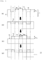
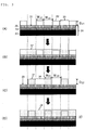
- patterned diamond 2 or 22 is prepared on the surface of the foundation 1 or 21 (a foundation surface) ( FIG. 1 (A) , FIG. 3 (A) ).
- the material for composing the foundation 1 and 21 is not particularly limited.
- the foundation surface is composed of diamond 3 as in FIG. 1
- a diamond substrate is manufactured by homoepitaxial growth.
- Illustrative examples of such a foundation 1 include diamond 3 such as diamond synthesized by an HPHT method, homoepitaxial diamond, and heteroepitaxial diamond. Particularly, a diamond substrate with even fewer defects can be manufactured by using diamond having relatively few defects such as diamond synthesized by an HPHT method and homoepitaxial diamond as a foundation.
- the foundation surface is composed of a different kind of material other than diamond as shown in FIG. 3 , a diamond substrate is manufactured by heteroepitaxial growth.
- the material be a cubic crystal like diamond, have small lattice mismatch with diamond, and do not form carbide through reaction with carbon.
- the material to meet these conditions include platinum group such as rhodium (Rh), palladium (Pd), iridium (Ir), and platinum (Pt).
- the lattice parameter of diamond is 3.57 ⁇ , and accordingly, the lattice mismatch with Rh (lattice parameter: 3.72 ⁇ ) is 4.2%, the lattice mismatch with Ir (lattice parameter: 3.84 ⁇ ) is 7.6%, and the lattice mismatch with Pt (lattice parameter: 3.92 ⁇ ) is 9.8%. It is preferable that the lattice mismatch between diamond and the different kind of material composing the foundation is 10% or less. In view of not forming carbide through reaction with carbon, Ir is preferable.
- Illustrative examples of the foundation 21 include a foundation in which the middle layer 24 composed of material selected from single crystal magnesium oxide (MgO), single crystal strontium titanate (SrTiO 3 ), ⁇ -alumina (Al 2 O 3 ), and yttria-stabilized zirconia (YSZ) is prepared on the silicon (Si) substrate 23; and the top layer 25 composed of material selected from iridium (Ir), rhodium (Rh), and platinum (Pt) is prepared on the middle layer.
- MgO single crystal magnesium oxide
- SrTiO 3 single crystal strontium titanate
- Al 2 O 3 ⁇ -alumina
- YSZ yttria-stabilized zirconia
- one or more layers composed of material selected from gold (Au), platinum (Pt), titanium (Ti), chromium (Cr), iridium (Ir), rhodium (Rh), silicon (Si), and silicon oxide (SiO 2 ) between the silicon (Si) substrate 23 and the middle layer 24.
- patterned in the present invention means a pattern formed of ruggedness.
- diamond 3 of the foundation surface can be processed into patterned diamond 2, for example, by a known method such as photolithography and electron beam lithography ( FIG. 1(A) ).
- the foundation is composed of a different kind of material
- diamond is grown on the foundation surface by a known method such as microwave plasma CVD, direct current plasma CVD, hot-filament CVD, and arc discharge plasma jet CVD.
- the patterned diamond 22 can be prepared on the foundation surface by processing the diamond grown on the foundation surface to a patterned shape by a method such as photolithography and electron beam lithography ( FIG. 3 (A) ).
- the foundation surface is composed of diamond
- any pattern shape of the patterned diamond 2 and 22 prepared on a foundation surface can be a pattern in which plural of diamonds each having line shape, rectangular dot shape, circular dot shape, etc. are arranged.
- the ratio D/W of a depth D (D 11 in FIG. 1 , D 21 in FIG. 3 ) to a width W (W 12 in FIG. 1 , W 22 in FIG. 3 ) of each pattern gap 10 and 30 of the patterned diamond 2 and 22 be 0.1 or more, more preferably 0.5 or more.
- W 11 in FIG. 1 and W 21 in FIG. 3 are the widths of the convex portion of the patterned diamond 2 and 22. This makes it possible to fill each pattern gaps 10 and 30 relatively early in the second step. Accordingly, even when an abnormal growth particle is generated from the pattern gap, it rarely influences the formed diamond surface.
- pattern gap in the present invention means a gap between the convex portions of patterned diamond.
- the bottom portions 11 and 31 of the pattern gaps 10 and 30 may be composed of diamond or a different kind of material.
- Materials such as MgO, however, are etched by hydrogen (H 2 ) / methane (CH 4 ) plasma of CVD when diamond is formed in a pattern gap in the second step. Accordingly, materials such as Ir are preferable.
- a foreign substance can adhere on the wall of the patterned diamond 2 and 22 prepared on the foundation surface in a step of processing the diamond into a patterned shape.
- a foreign substance caused by SiO 2 used as a mask can adhere. It is preferable to remove these foreign substances adhered onto the wall of the patterned diamond prepared on the foundation surface, before the second step. Such removal of a foreign substance adhered onto the diamond wall can suppress generation of abnormal growth particles in the second step.
- the removal of a foreign substance can be performed by selective etching, for example.
- a foreign substance such as Ir or SiO 2
- CF 4 plasma when a foreign substance such as Ir or SiO 2 is adhering on a wall of the patterned diamond 2 and 22 prepared on the foundation surface, it can be removed by etching with CF 4 plasma.
- the foundation surface is composed of a different kind of material other than diamond
- etching can be mentioned, for example.
- diamond is grown from the patterned diamond 2 or 22 prepared in the first step to form the diamond 12 or 32 in the pattern gap 10 or 30 of the patterned diamond 2 or 22 prepared in the first step ( FIG. 1 (B) , FIG. 3 (B) ).
- the method for growing the diamond 12 or 32 from the patterned diamond prepared in the first step can be selected from a known method such as microwave plasma CVD, direct current plasma CVD, hot-filament CVD, and arc discharge plasma jet CVD.
- diamond is laterally grown from the patterned diamond as a nucleus (ELO: Epitaxial Lateral Overgrowth). Accordingly, diamond 12 or 32 with few defects can be formed in the pattern gap.
- ELO Epitaxial Lateral Overgrowth
- the diamond does not have to be formed so as to fill the whole pattern gaps.
- a void can be formed in the bottom portion of the pattern gap. Forming such a void can relax stress, especially thermal stress created when the foundation is composed of a different kind of material, and is preferable thereby.
- the void to be formed can be a void having a nearly triangle shape cross-section of a side 0.01 to 20 ⁇ m, for example.
- the patterned diamond 2 or 22 prepared in the first step is removed to form a patterned diamond 13 or 33 composed of the diamond formed in the second step ( FIG. 1 (C) , FIG. 3 (C) ).
- This step can be performed by using a known method such as photolithography or electron beam lithography.
- this step it is not necessary to remove the whole patterned diamond 2 or 22 prepared in the first step. It is also possible to remove a part of the diamond 12 or 32 formed in the second step, as needed.
- the diamond 12 or 32 formed in the second step is removed to a position which is 5 ⁇ m or more away from a boundary with the patterned diamond 2 or 22 prepared in the first step.
- the region to be removed is preferably limited to a position which is 30 ⁇ m or less away from a boundary with the patterned diamond 2 or 22 prepared in the first step.
- any pattern shape of the patterned diamond 13 or 33 as in the first step it is possible to select any pattern shape of the patterned diamond 13 or 33 as in the first step.
- it can be a pattern in which plural of diamonds each having line shape, rectangular dot shape, circular dot shape, etc. are arranged.
- each pattern gap 14 and 34 of the patterned diamond 13 and 33 it is also possible to select any position, any size, any thickness, and any crystal orientation of each patterned diamond 13 and 33.
- the ratio D/W of a depth D (D 12 in FIG. 1 , D 22 in FIG. 3 ) to a width W (W 14 in FIG. 1 , W 24 in FIG. 3 ) of each pattern gap 14 and 34 of the patterned diamond 13 and 33 be 0.1 or more, more preferably 0.5 or more.
- W 13 in FIG. 1 and W 23 in FIG. 3 are the widths of the convex portion of the patterned diamond 13 and 33. This makes it possible to fill each pattern gap 14 and 34 relatively early in the fourth step. Accordingly, even when an abnormal growth particle is generated from each pattern gap 14 and 34, it rarely influences the formed diamond surface.
- the bottom portions 15 and 35 of the pattern gaps 14 and 34 may be composed of diamond or a different kind of material. Materials such as MgO, however, are etched by hydrogen (H 2 )/ methane (CH 4 ) plasma of CVD when diamond is formed in a pattern gap in the fourth step. Accordingly, materials such as Ir are preferable.
- a foreign substance can adhere on the wall of the patterned diamond in a step of processing the diamond into a patterned shape.
- a foreign substance caused by SiO 2 used as a mask can adhere. It is preferable to remove these foreign substances adhered onto the diamond wall, before the fourth step. By removing a foreign substance adhered onto the diamond wall can suppress generation of abnormal growth particles in the fourth step.
- the removal of a foreign substance can be performed by selective etching, for example.
- Ir or SiO 2 when adhering on a diamond wall, it can be removed by etching with CF 4 plasma.
- the foundation surface is composed of a different kind of material other than diamond
- at least a part of the bottom portion 35, which are bottoms of the pattern gap 34 of the patterned diamond 33 formed in the third step, may be prepared below the foundation surface, by removing a part of the foundation too.
- diamond is grown from the patterned diamond 13 or 33 formed in the third step to form the diamond 16 or 36 in the pattern gap 14 or 34 of the patterned diamond 13 or 33 formed in the third step ( FIG. 1 (D) , FIG. 3 (D) ).
- the method for growing the diamond from the patterned diamond formed in the third step can be selected from a known method such as microwave plasma CVD, direct current plasma CVD, hot-filament CVD, and arc discharge plasma jet CVD as in the second step.
- diamond is laterally grown from the patterned diamond as a nucleus (ELO: Epitaxial Lateral Overgrowth). Accordingly, diamond with few defects is formed in the pattern gap.
- ELO Epitaxial Lateral Overgrowth
- the diamond also does not have to be formed so as to fill the whole pattern gaps 14 and 34. It is preferable to form a void in the bottom portion 15 and 35 of each pattern gap. In each of the second and fourth steps, formation of such a void can relax stress, especially thermal stress created when the foundation is composed of a different kind of material.
- the present invention can manufacture the diamond substrate 17 and 37 in which the whole surface is composed of lateral grown diamond and/or diamond grown from the lateral grown diamond through the steps from the first to the fourth.
- the present invention provide a diamond substrate in which at least one surface is composed of diamond, and the whole surface of at least one surface is composed of at least one of lateral grown diamond and diamond grown from the lateral grown diamond.
- the whole surface does not have to be lateral grown diamond and/or diamond grown from the lateral grown diamond before the fourth step. It is also possible to manufacture the diamond substrate in which the whole surface of at least one surface is composed of at least one of lateral grown diamond and diamond grown from the lateral grown diamond by repeating the formation and growth of patterned diamond according to the third step and the fourth step for plural times.
- the diamond substrate manufactured by the present invention may be used with the foundation being remained, or may be used as a freestanding substrate with the foundation being removed.
- the thickness of the freestanding substrate is preferably 50 ⁇ m or more and 2000 ⁇ m or less.
- the freestanding substrate with a thickness of 50 ⁇ m or more is easy to be handled and does not have a risk of breakage in its production process or in a device production process using the diamond substrate, and is preferable thereby.
- the thickness of the freestanding substrate is 2000 ⁇ m or less
- the time for forming the diamond does not become longer in itself, and the time for polishing process can be shortened since the surface of the diamond substrate does not have large ruggedness. Accordingly, the production cost can be reduced. It is also possible to suppress warpage of the substrate, and to suppress generation of a crack and breakage.
- the diamond layer does not have to be formed needlessly thick.
- the thickness from the foundation surface to the surface of the substrate be 300 ⁇ m or less.
- a void is formed in the bottom portion of a pattern gap in the second and/or the fourth step, it is possible to obtain a diamond substrate 100 in which at least one surface 101 is composed of diamond, and the inner portion contains voids 52 as shown in FIG. 5 .
- the inventive diamond substrate 100 can comprise the foundation 50 and the diamond layer 51 formed on the surface of the foundation 50, and can contain the void(s) 52 on the boundary between the foundation 50 and the diamond layer 51.
- a diamond substrate comprising a foundation and a diamond layer formed on the surface of the foundation, wherein a back surface of the foundation has an opening.
- the defects are sufficiently reduced, and the internal stress created as the crystal growth and the thermal stress are reduced. Accordingly, it is possible to suppress warpage of the substrate and generation of a crack.
- the surface of a diamond substrate manufactured by the present invention is composed of single crystal diamond.
- B boron
- P phosphorous
- a diamond substrate was manufactured by the method shown in FIG. 3 .
- a patterned diamond 22 was prepared on the surface of a foundation 21 as shown in FIG. 3 (A) (the first step). Specifically, the patterned diamond 22 was prepared on the surface of the foundation 21 through the steps shown in FIG. 4 (a) to FIG. 4 (f) .
- the foundation 21 was produced, and a diamond layer 26 was formed on the foundation 21 as follows ( FIG. 4 (a) ).
- a double-side polished single crystal silicon (Si) substrate 23 having a diameter of 10.0 mm and a thickness of 1.0 mm, with the surface having a (100) plane was prepared.
- a layer 24 composed of single crystal MgO was formed by electron beam deposition.
- the single crystal MgO layer 24 was epitaxially grown until the thickness reached to 1 ⁇ m under the conditions of 900°C of the substrate temperature in vacuum.
- a layer 25 composed of Ir was formed on this single crystal MgO layer 24, a layer 25 composed of Ir was formed.
- the Ir layer 25 was formed by using a radio-frequency (RF) magnetron sputtering method (13.56 MHz) with targeting at Ir having a diameter of 6 inches (150 mm), a thickness of 5.0 mm, and purity of 99.9% or higher.
- the substrate on which the single crystal MgO layer 24 had been formed was heated to 800°C, and after it was confirmed that a base pressure became 6 ⁇ 10 -7 Torr (about 8.0 ⁇ 10 -5 Pa) or lower, 10 sccm of Ar gas was introduced. After the pressure became 5 ⁇ 10 -2 Torr (about 6.7 Pa) by adjusting aperture of a valve connected to an exhaust system, film formation was performed for 15 minutes by inputting RF power of 1000 W.
- the obtained Ir layer 25 had a thickness of 0.7 ⁇ m.
- the foundation 21 was subjected to pre-treatment (bias treatment) in order to form diamond nuclei.
- the foundation was set on a planar electrode having a diameter of 15 mm, with the Ir layer 25 side facing upwards.
- the pressure became 100 Torr (about 1.3 ⁇ 10 4 Pa) by adjusting aperture of the valve connected to the exhaust system, a negative voltage was applied to an electrode at the substrate side to expose the foundation to plasma for 90 seconds, and thereby the surface of the foundation was subjected to bias treatment.
- a diamond layer 26 was heteroepitaxially grown on the foundation surface using a direct current plasma CVD method.
- the obtained diamond layer 26 was a complete continuous film which did not have delamination on the whole surface of the substrate with a diameter of 10 mm, and had a film thickness of 10 ⁇ m.
- the etch-pit density was also evaluated.
- the surface of the diamond layer 26 was subjected to plasma treatment under the conditions of H 2 gas 100 vol.%. 0.8 Pa, 2200 W, and 1 hour by using a microwave (2.45 GHz) plasma CVD apparatus, and then the etch-pit density was measured by SEM observation to be 8 ⁇ 10 8 (cm -2 ).
- the diamond layer 26 was subjected to patterning.
- 1000 nm of SiO 2 film 27 was formed on the diamond layer by an RF plasma CVD method using tetraethyl orthosilicate (TEOS) as a raw material ( FIG. 4(b) ).
- TEOS tetraethyl orthosilicate
- a resist pattern 28 was formed ( FIG. 4 (c) ).
- a titanium (Ti) film and a gold (Au) film were formed successively and subjected to liftoff, thereby forming the SiO 2 film 27 and the titanium (Ti)/gold (Au) pattern 29 successively on the diamond layer 26 ( FIG. 4 (d) ).
- SiO 2 etching was performed by using CF 4 gas to make a hard mask for diamond etching ( FIG. 4 (e) ).
- the diamond layer was etched under the conditions of O 2 gas 100 vol.%, 2.0 Pa, 500 W, and 900 seconds by using an induced combination plasma etching equipment ( FIG. 4 (f) ).
- the patterned diamond 22 was prepared on the surface of the foundation ( FIG. 3 (A) ).
- the patterned diamond 22 in FIG. 3 (A) had a pattern in which 50 ⁇ m square (i.e., W 21 is 50 ⁇ m) rectangular dot diamonds were arranged, and a width of the pattern gap W 22 of 70 ⁇ m.
- W 21 is 50 ⁇ m
- W 22 a width of the pattern gap W 22 of 70 ⁇ m.
- the directions of the grooves were two directions which were perpendicular with each other, and one of them was the same direction with the [011] orientation of the diamond layer.
- the depth D 21 of the pattern gap was 10 ⁇ m, and the ratio (D 21 /W 22 ) of the depth D 21 to the width W 22 of the pattern gap was 0.14 in this case.
- the bottom portion of the pattern gap was in a state in which Ir of the foundation was exposed.
- the obtained patterned diamond was cleaned by plasma treatment ( FIG. 4 (g) ).
- the treatment was performed under the conditions of CF 4 gas 100 vol.%, 2.0 Pa, 500 W, and 650 seconds by using an induced combination plasma etching equipment. This procedure could remove foreign substances probably due to Ir adhered on the wall of the patterned diamond.
- the hard mask of SiO 2 was removed with buffered hydrofluoric acid, and cleaned with a thermal mixed acid ( FIG. 4 (h) ).
- the diamond 32 was grown from the patterned diamond 22, which had been prepared on the foundation surface, by a microwave plasma CVD method, in the pattern gap 30 of the patterned diamond prepared in the first step ( FIG. 3 (B) ).
- the pattern gaps were filled.
- the thickness from the foundation surface to the surface of the substrate was 103 ⁇ m.
- the etch-pit density was also evaluated.
- the surface of the diamond layer was subjected to plasma treatment under the conditions of H 2 gas 100 vol.%. 0.8 Pa, 2200 W, and 1 hour by using a microwave (2.45 GHz) plasma CVD apparatus. Then, the etch-pit densities were measured by SEM observation, and found that the portion grown on the patterned diamond showed 1 ⁇ 10 8 (cm -2 ), on the other hand, the portion of the pattern gap showed 3 ⁇ 10 6 (cm -2 ), that is, the etch-pit density was decreased about two orders of magnitude.
- the change of warpage of the back surface of the substrate before and after the formation of the diamond layer was measured by using an optical interference or a contact type measuring device. Subsequently, this measured value was divided by an increment of the film thickness before and after the formation of the diamond layer, and the calculated value was defined to the evaluation value of stress of the diamond substrate.
- the evaluation value in this case was 21 ⁇ 10 -2 .
- the surface of the obtained diamond substrate was polished. After the polishing, the thickness from the foundation surface to the surface of the substrate was 71 ⁇ m, and the surface roughness RMS was 0.3 nm (AFM measurement, in a region of 10 ⁇ m square).
- the second patterning of the diamond layer was performed by the same process as in the first patterning to form patterned diamond 33 composed of the diamond 32 formed in the second step ( FIG. 3 (C) ).
- the pattern shape in this case was a pattern in which 50 ⁇ m square (i.e., W 23 was 50 ⁇ m) rectangular dot diamonds were arranged, and a width of the pattern gap W 24 was 70 ⁇ m as in the shape of the first pattern. Provided that, the position of the pattern was translated in parallel along the [011] orientation of the diamond layer by 60 ⁇ m with respect to the first pattern.
- the diamond 32 formed in the second step was removed to a position which was 10 ⁇ m away from the boundary with the patterned diamond 22 prepared in the first step.
- diamond 36 was grown from the patterned diamond 33, using the same method as in growing the diamond from the patterned diamond prepared on the foundation surface, in the pattern gap 34 of the patterned diamond formed in the third step ( FIG. 3 (D) ).
- the pattern gaps were filled.
- the thickness from the foundation surface to the surface of the substrate was 164 ⁇ m.
- the etch-pit density was also evaluated.
- the surface of the diamond layer was subjected to plasma treatment under the conditions of H 2 gas 100 vol.%. 0.8 Pa, 2200 W, and 1 hour by using a microwave (2.45 GHz) plasma CVD apparatus. Then, the etch-pit densities were measured by SEM observation, and found that the both of the portion grown on the patterned diamond and the portion of the pattern gap showed 3 ⁇ 10 6 (cm -2 ), that is, the etch-pit densities were low in the whole surface of the diamond substrate 37.
- a diamond substrate was manufactured by the method shown in FIG. 1 .
- a patterned diamond 2 was prepared on the surface of a foundation 1 as shown in FIG. 1 (A) (the first step). Specifically, the patterned diamond 2 was prepared through the steps shown in FIG. 2(a) to FIG. 2(f) .
- a double-side polished heteroepitaxial diamond substrate (freestanding substrate) 6 having a diameter of 5.0 mm and a thickness of 0.5 mm, with the surface having a (100) plane was prepared. This was cleaned with a thermal mixed acid, and used as a foundation 1 ( FIG. 2 (a) ).
- SiO 2 film 7 was formed on the diamond layer by an RF plasma CVD method using tetraethyl orthosilicate (TEOS) as a raw material ( FIG. 2 (b) ).
- TEOS tetraethyl orthosilicate
- a resist pattern 8 was formed ( FIG. 2(c) ).
- a titanium (Ti) film and a gold (Au) film were formed successively and subjected to liftoff, thereby forming the SiO 2 film 7 and the titanium (Ti)/gold (Au) pattern 9 successively on the diamond substrate 6 ( FIG. 2 (d) ).
- SiO 2 etching was performed by using CF 4 gas to make a hard mask for diamond etching ( FIG. 2 (e) ).
- the diamond layer was etched under the conditions of O 2 gas 100 vol.%, 2.0 Pa, 500 W, and 900 seconds by using an induced combination plasma etching equipment ( FIG. 2 (f) ).
- the patterned diamond 2 was prepared on the surface of the foundation ( FIG. 1 (A) ).
- the pattern shape in FIG. 1 (A) was a pattern in which 50 ⁇ m square (i.e., W 11 is 50 ⁇ m) rectangular dot diamonds were arranged, and a width of the pattern gap W 12 was 70 ⁇ m.
- this was a pattern in which plural grooves were provided in parallel with each other on the diamond layer, and other plural grooves being in parallel with each other were provided perpendicular to the foregoing grooves.
- the directions of the grooves were two directions which were perpendicular with each other, and one of them was the same direction with the [011] orientation of the diamond layer.
- the depth D 11 of the pattern gap of the patterned diamond 2 was adjusted to 10 ⁇ m, and accordingly, the ratio (D 11 /W 12 ) of the depth D 11 to the width W 12 of the patterned diamond was 0.14 in this case.
- the obtained patterned diamond was cleaned by plasma treatment ( FIG. 2 (g) ).
- the treatment was performed under the conditions of CF 4 gas 100 vol.%, 2.0 Pa, 500 W, and 650 seconds by using an induced combination plasma etching equipment.
- the hard mask of SiO 2 was removed with buffered hydrofluoric acid, and cleaned with a thermal mixed acid ( FIG. 2 (h) ).
- the diamond 12 was grown from the patterned diamond 2, which had been prepared on the foundation surface, by a microwave plasma CVD method in the pattern gap 10 of the patterned diamond prepared in the first step ( FIG. 1 (B) ).
- the pattern gaps were filled.
- the thickness from the foundation surface to the surface of the substrate was 78 ⁇ m.
- the etch-pit density was also evaluated.
- the surface of the diamond layer was subjected to plasma treatment under the conditions of H 2 gas 100 vol.%. 0.8 Pa, 2200 W, and 1 hour by using a microwave (2.45 GHz) plasma CVD apparatus. Then, the etch-pit densities were measured by SEM observation, and found that the portion grown on the patterned diamond showed 2 ⁇ 10 8 (cm -2 ), on the other hand, the portion of the pattern gap showed 4 ⁇ 10 6 (cm -2 ), that is, the etch-pit density was decreased about two orders of magnitude.
- the cross section of the substrate was observed under SEM to reveal that the portions where had been pattern gaps were entirely filled.
- the surface of the obtained diamond substrate was polished. After the polishing, the thickness from the foundation surface to the surface of the substrate was 56 ⁇ m, and the surface roughness RMS was 0.3 nm (AFM measurement, in a region of 10 ⁇ m square).
- the second patterning of the diamond layer was performed by the same process as in the first patterning to form patterned diamond 13 composed of the diamond formed in the second step ( FIG. 1 (C) ).
- the pattern shape in this case was a pattern in which 50 ⁇ m square (i.e., W 13 was 50 ⁇ m) rectangular dot diamonds were arranged, and a width of the pattern gap W 14 was 70 ⁇ m as in the shape of the first pattern.
- the position of the pattern was translated in parallel along the [011] orientation of the diamond layer by 60 ⁇ m with respect to the first pattern. That is, in this case, the diamond formed in the second step was removed to a position which was 10 ⁇ m away from a boundary with the patterned diamond prepared in the first step.
- diamond 16 was grown from the patterned diamond 13 by the same method as in growing the diamond from the patterned diamond prepared on the foundation surface ( FIG. 1 (D) ).
- the pattern gaps were filled.
- the thickness from the foundation surface to the surface of the substrate was 134 ⁇ m.
- the etch-pit density was also evaluated.
- the surface of the diamond layer was subjected to plasma treatment under the conditions of H 2 gas 100 vol.%. 0.8 Pa, 2200 W, and 1 hour by using a microwave (2.45 GHz) plasma CVD apparatus. Then, the etch-pit densities were measured by SEM observation, and found that the portion grown on the patterned diamond showed 3 ⁇ 10 6 (cm -2 ), and the portion of the pattern gap showed 4 ⁇ 10 6 (cm -2 ), that is, the etch-pit densities were low in the whole surface of the diamond substrate.
- the cross section of the obtained diamond substrate 17 was observed under SEM to reveal that the portions where had been pattern gaps were entirely filled.
- a double-side polished single crystal silicon (Si) substrate having a diameter of 10.0 mm and a thickness of 1.0 mm, with the surface having a (100) plane was prepared.
- a layer composed of single crystal MgO was formed by electron beam deposition.
- the single crystal MgO layer was epitaxially grown until the thickness reached to 1 ⁇ m under the conditions of 900°C of the substrate temperature in vacuum.
- a layer composed of Ir was formed on this single crystal MgO layer.
- the Ir layer was formed by using a radio-frequency (RF) magnetron sputtering method (13.56 MHz) with targeting at Ir having a diameter of 6 inches (150 mm), a thickness of 5.0 mm, and purity of 99.9% or higher.
- RF radio-frequency
- the substrate on which the single crystal MgO layer had been formed was heated to 800°C, and after it was confirmed that a base pressure became 6 ⁇ 10 -7 Torr (about 8.0 ⁇ 10 -5 Pa) or lower, 10 sccm of Ar gas was introduced. After the pressure became 5 ⁇ 10 -2 Torr (about 6.7 Pa) by adjusting aperture of the valve connected to the exhaust system, film formation was performed for 15 minutes by inputting RF power of 1000 W.
- the obtained Ir layer had a thickness of 0.7 ⁇ m.
- the foundation was subjected to pre-treatment (bias treatment) in order to form diamond nuclei.
- bias treatment bias treatment
- a diamond layer was heteroepitaxially grown on the foundation surface using a direct current plasma CVD method.
- the obtained diamond layer was a complete continuous film which did not have delamination on the whole surface of the substrate with a diameter of 10 mm, and had a film thickness of 10 ⁇ m.
- the etch-pit density was also evaluated.
- the surface of the diamond layer was subjected to plasma treatment under the conditions of H 2 gas 100 vol.%. 0.8 Pa, 2200 W, and 1 hour by using a microwave (2.45 GHz) plasma CVD apparatus, and then the etch-pit density was measured by SEM observation to be 8 ⁇ 10 8 (cm -2 ).
- the obtained diamond layer was a complete continuous film which did not have delamination on the whole surface of the substrate with a diameter of 10 mm, and had a film thickness of 90 ⁇ m.
- the etch-pit density was also evaluated.
- the surface of the diamond layer was subjected to plasma treatment under the conditions of H 2 gas 100 vol.%. 0.8 Pa, 2200 W, and 1 hour by using a microwave (2.45 GHz) plasma CVD apparatus, and then the etch-pit density was measured by SEM observation to be 4 ⁇ 10 8 (cm -2 ).
- the inventive method for manufacturing a diamond substrate can give a high-quality diamond substrate with sufficiently reduced defects and low stress. It has been also revealed that in the inventive diamond substrate, defects are sufficiently reduced, and the stress is decreased.
Landscapes
- Chemical & Material Sciences (AREA)
- Engineering & Computer Science (AREA)
- Crystallography & Structural Chemistry (AREA)
- Materials Engineering (AREA)
- Metallurgy (AREA)
- Organic Chemistry (AREA)
- Chemical Kinetics & Catalysis (AREA)
- General Chemical & Material Sciences (AREA)
- Crystals, And After-Treatments Of Crystals (AREA)
- Chemical Vapour Deposition (AREA)
- Carbon And Carbon Compounds (AREA)
Applications Claiming Priority (1)
| Application Number | Priority Date | Filing Date | Title |
|---|---|---|---|
| JP2016037175A JP6679022B2 (ja) | 2016-02-29 | 2016-02-29 | ダイヤモンド基板の製造方法 |
Publications (2)
| Publication Number | Publication Date |
|---|---|
| EP3211657A2 true EP3211657A2 (fr) | 2017-08-30 |
| EP3211657A3 EP3211657A3 (fr) | 2017-11-15 |
Family
ID=58264335
Family Applications (1)
| Application Number | Title | Priority Date | Filing Date |
|---|---|---|---|
| EP17000294.3A Ceased EP3211657A3 (fr) | 2016-02-29 | 2017-02-23 | Procédé de fabrication de substrat de diamant, substrat de diamant et substrat de diamant autonome |
Country Status (6)
| Country | Link |
|---|---|
| US (2) | US10253426B2 (fr) |
| EP (1) | EP3211657A3 (fr) |
| JP (1) | JP6679022B2 (fr) |
| KR (1) | KR102728345B1 (fr) |
| CN (1) | CN107130294B (fr) |
| TW (1) | TWI745350B (fr) |
Cited By (1)
| Publication number | Priority date | Publication date | Assignee | Title |
|---|---|---|---|---|
| WO2020008044A1 (fr) * | 2018-07-06 | 2020-01-09 | Element Six Technologies Limited | Procédé de fabrication d'un matériau de diamant synthétique monocristallin |
Families Citing this family (12)
| Publication number | Priority date | Publication date | Assignee | Title |
|---|---|---|---|---|
| US12065357B2 (en) * | 2015-02-09 | 2024-08-20 | Saeed Alhassan Alkhazraji | Process for manufacturing a pure porous 3D diamond |
| US10494713B2 (en) | 2015-04-16 | 2019-12-03 | Ii-Vi Incorporated | Method of forming an optically-finished thin diamond film, diamond substrate, or diamond window of high aspect ratio |
| GB2562918B (en) * | 2016-03-18 | 2021-01-27 | Mitsubishi Electric Corp | Semiconductor device and method of manufacturing semiconductor device |
| CN110241386B (zh) * | 2018-03-09 | 2024-02-09 | 深圳先进技术研究院 | 一种掺硼金刚石电极及其制备方法和应用 |
| CN108598036B (zh) * | 2018-06-26 | 2020-03-27 | 苏州汉骅半导体有限公司 | 金刚石基氮化镓器件制造方法 |
| FR3091299B1 (fr) * | 2018-12-28 | 2021-01-29 | Commissariat Energie Atomique | Procédé de formation d’un film de diamant hétéroépitaxié sur un substrat en iridium monocristallin |
| US12519030B2 (en) * | 2019-06-18 | 2026-01-06 | Mitsubishi Electric Corporation | Semiconductor device including diamond substrate and semiconductor device manufacturing method |
| CN111206280B (zh) * | 2020-01-07 | 2021-02-12 | 北京科技大学 | 一种高质量大尺寸单晶金刚石外延生长的方法 |
| KR102393733B1 (ko) * | 2020-05-07 | 2022-05-06 | 한국세라믹기술원 | 반도체용 다이아몬드 박막 제조방법 |
| WO2022192666A1 (fr) * | 2021-03-12 | 2022-09-15 | Akash Systems, Inc. | Éléments de substrat dans des matériaux thermiquement conducteurs |
| CN113716560A (zh) * | 2021-07-15 | 2021-11-30 | 哈尔滨工业大学(威海) | 一种人造金刚石表面刻蚀的方法 |
| KR102866978B1 (ko) * | 2023-10-26 | 2025-09-30 | 한국핵융합에너지연구원 | 다이아몬드 웨이퍼 제조방법 |
Citations (2)
| Publication number | Priority date | Publication date | Assignee | Title |
|---|---|---|---|---|
| US20110081531A1 (en) * | 2009-10-02 | 2011-04-07 | Shin-Etsu Chemical Co., Ltd. | Base material for growing single crystal diamond and method for producing single crystal diamond substrate |
| WO2015197632A1 (fr) * | 2014-06-23 | 2015-12-30 | Univ Paris Xiii Paris-Nord Villetaneuse | Procede de formation d'un monocristal de materiau a partir d'un substrat monocristallin |
Family Cites Families (25)
| Publication number | Priority date | Publication date | Assignee | Title |
|---|---|---|---|---|
| US4925701A (en) * | 1988-05-27 | 1990-05-15 | Xerox Corporation | Processes for the preparation of polycrystalline diamond films |
| GB2228745B (en) * | 1989-01-10 | 1993-09-08 | Kobe Steel Ltd | Process for the selective deposition of thin diamond film by gas phase synthesis |
| US5242711A (en) * | 1991-08-16 | 1993-09-07 | Rockwell International Corp. | Nucleation control of diamond films by microlithographic patterning |
| US5989511A (en) * | 1991-11-25 | 1999-11-23 | The University Of Chicago | Smooth diamond films as low friction, long wear surfaces |
| US5614019A (en) * | 1992-06-08 | 1997-03-25 | Air Products And Chemicals, Inc. | Method for the growth of industrial crystals |
| JPH06247793A (ja) | 1993-02-22 | 1994-09-06 | Sumitomo Electric Ind Ltd | 単結晶ダイヤモンドおよび製造法 |
| US5552345A (en) * | 1993-09-22 | 1996-09-03 | Harris Corporation | Die separation method for silicon on diamond circuit structures |
| US5686152A (en) * | 1995-08-03 | 1997-11-11 | Johnson; Linda F. | Metal initiated nucleation of diamond |
| US6940098B1 (en) | 1999-03-17 | 2005-09-06 | Mitsubishi Cable Industries, Ltd. | Semiconductor base and its manufacturing method, and semiconductor crystal manufacturing method |
| JP3587081B2 (ja) * | 1999-05-10 | 2004-11-10 | 豊田合成株式会社 | Iii族窒化物半導体の製造方法及びiii族窒化物半導体発光素子 |
| DE10039208A1 (de) * | 2000-08-10 | 2002-04-18 | Fraunhofer Ges Forschung | Verfahren zur Herstellung eines Werkzeugs, das zur Schaffung optisch wirksamer Oberflächenstrukturen im sub-mum Bereich einsetzbar ist, sowie ein diesbezügliches Werkzeug |
| CN1300387C (zh) * | 2004-11-12 | 2007-02-14 | 南京大学 | 无掩膜横向外延生长高质量氮化镓 |
| US8470701B2 (en) * | 2008-04-03 | 2013-06-25 | Advanced Diamond Technologies, Inc. | Printable, flexible and stretchable diamond for thermal management |
| US8624263B2 (en) * | 2008-04-17 | 2014-01-07 | National Institute Of Advanced Industrial Science And Technology | Diamond semiconductor device and method of manufacturing the same |
| JP2010222172A (ja) * | 2009-03-23 | 2010-10-07 | Nippon Telegr & Teleph Corp <Ntt> | ダイヤモンド薄膜及びその製造方法 |
| US9277792B2 (en) * | 2010-08-24 | 2016-03-08 | Board Of Trustees Of Michigan State University | Multicolored single crystal diamond gemstones and methods for forming the same |
| US20120288698A1 (en) * | 2011-03-23 | 2012-11-15 | Advanced Diamond Technology, Inc | Method of fabrication, device structure and submount comprising diamond on metal substrate for thermal dissipation |
| JP5831795B2 (ja) * | 2011-09-06 | 2015-12-09 | 住友電気工業株式会社 | ダイヤモンド複合体およびそれから分離した単結晶ダイヤモンド |
| SG195494A1 (en) * | 2012-05-18 | 2013-12-30 | Novellus Systems Inc | Carbon deposition-etch-ash gap fill process |
| WO2015199180A1 (fr) * | 2014-06-25 | 2015-12-30 | 住友電気工業株式会社 | Procédé de production de substrat en diamant, substrat en diamant, et substrat composite en diamant |
| EP3421637B1 (fr) * | 2014-08-11 | 2020-10-14 | Sumitomo Electric Industries, Ltd. | Diamant |
| CN104651928A (zh) * | 2015-01-17 | 2015-05-27 | 王宏兴 | 金刚石同质外延横向生长方法 |
| CN104724664A (zh) * | 2015-03-14 | 2015-06-24 | 王宏兴 | 单晶金刚石纳米柱阵列结构的制备方法和应用 |
| CN104775154B (zh) * | 2015-04-25 | 2017-06-27 | 哈尔滨工业大学 | 一种同质外延生长单晶金刚石时控制表面温度的方法 |
| JP6699015B2 (ja) * | 2016-02-29 | 2020-05-27 | 信越化学工業株式会社 | ダイヤモンド基板の製造方法 |
-
2016
- 2016-02-29 JP JP2016037175A patent/JP6679022B2/ja active Active
-
2017
- 2017-02-22 KR KR1020170023624A patent/KR102728345B1/ko active Active
- 2017-02-23 EP EP17000294.3A patent/EP3211657A3/fr not_active Ceased
- 2017-02-23 TW TW106106033A patent/TWI745350B/zh active
- 2017-02-24 CN CN201710106146.8A patent/CN107130294B/zh active Active
- 2017-02-28 US US15/445,134 patent/US10253426B2/en active Active
-
2018
- 2018-11-02 US US16/179,363 patent/US11066757B2/en active Active
Patent Citations (2)
| Publication number | Priority date | Publication date | Assignee | Title |
|---|---|---|---|---|
| US20110081531A1 (en) * | 2009-10-02 | 2011-04-07 | Shin-Etsu Chemical Co., Ltd. | Base material for growing single crystal diamond and method for producing single crystal diamond substrate |
| WO2015197632A1 (fr) * | 2014-06-23 | 2015-12-30 | Univ Paris Xiii Paris-Nord Villetaneuse | Procede de formation d'un monocristal de materiau a partir d'un substrat monocristallin |
Non-Patent Citations (5)
| Title |
|---|
| A. SAWABE ET AL., J. JPN. ASSOCIATION FOR CRYSTAL GROWTH, vol. 39, 2012, pages 179 |
| H. UMEZAWA ET AL., DIAMOND RELAT. MATER., vol. 18, 2009, pages 1196 |
| H. YAMADA ET AL., APPL. PHYS. LETT., vol. 104, 2014, pages 102110 |
| K. ICHIKAWA ET AL., PROC. 24TH NDF-DIA. SYMPO., vol. 226, 2010 |
| K. OHTSUKA ET AL., JPN. J. APPL. PHYS., vol. 35, 1996, pages L1072 |
Cited By (3)
| Publication number | Priority date | Publication date | Assignee | Title |
|---|---|---|---|---|
| WO2020008044A1 (fr) * | 2018-07-06 | 2020-01-09 | Element Six Technologies Limited | Procédé de fabrication d'un matériau de diamant synthétique monocristallin |
| US11643750B2 (en) | 2018-07-06 | 2023-05-09 | Element Six Technologies Limited | Method of manufacture of single crystal synthetic diamond material |
| US12065756B2 (en) | 2018-07-06 | 2024-08-20 | Element Six Technologies Limited | Method of manufacture of single crystal synthetic diamond material |
Also Published As
| Publication number | Publication date |
|---|---|
| US20170247811A1 (en) | 2017-08-31 |
| CN107130294B (zh) | 2021-05-28 |
| TWI745350B (zh) | 2021-11-11 |
| KR102728345B1 (ko) | 2024-11-08 |
| JP2017154908A (ja) | 2017-09-07 |
| TW201800627A (zh) | 2018-01-01 |
| US11066757B2 (en) | 2021-07-20 |
| US20190093253A1 (en) | 2019-03-28 |
| CN107130294A (zh) | 2017-09-05 |
| US10253426B2 (en) | 2019-04-09 |
| KR20170101798A (ko) | 2017-09-06 |
| EP3211657A3 (fr) | 2017-11-15 |
| JP6679022B2 (ja) | 2020-04-15 |
Similar Documents
| Publication | Publication Date | Title |
|---|---|---|
| US11066757B2 (en) | Diamond substrate and freestanding diamond substrate | |
| US10100435B2 (en) | Method for manufacturing diamond substrate | |
| US9200379B2 (en) | Base material for growing single crystal diamond and method for producing single crystal diamond substrate | |
| TWI787234B (zh) | 鑽石成膜用基底基板、以及使用其之鑽石基板的製造方法 | |
| US20110081531A1 (en) | Base material for growing single crystal diamond and method for producing single crystal diamond substrate | |
| JP5346052B2 (ja) | ダイヤモンド薄膜及びその製造方法 | |
| JP2021166293A (ja) | ダイヤモンド電子素子及びダイヤモンド電子素子の製造方法 | |
| JP7226722B2 (ja) | ダイヤモンド基板 | |
| US20250154685A1 (en) | Underlying substrate, single crystal diamond laminate substrate and method for producing them | |
| JP2022109306A (ja) | ダイヤモンド製膜用下地基板及びそれを用いたダイヤモンド基板の製造方法 | |
| US20260068551A1 (en) | Underlying substrate, single crystal diamond laminate substrate and method for producing them | |
| JP7487702B2 (ja) | 単結晶ダイヤモンド基板の製造方法 |
Legal Events
| Date | Code | Title | Description |
|---|---|---|---|
| PUAI | Public reference made under article 153(3) epc to a published international application that has entered the european phase |
Free format text: ORIGINAL CODE: 0009012 |
|
| STAA | Information on the status of an ep patent application or granted ep patent |
Free format text: STATUS: THE APPLICATION HAS BEEN PUBLISHED |
|
| AK | Designated contracting states |
Kind code of ref document: A2 Designated state(s): AL AT BE BG CH CY CZ DE DK EE ES FI FR GB GR HR HU IE IS IT LI LT LU LV MC MK MT NL NO PL PT RO RS SE SI SK SM TR |
|
| AX | Request for extension of the european patent |
Extension state: BA ME |
|
| PUAL | Search report despatched |
Free format text: ORIGINAL CODE: 0009013 |
|
| AK | Designated contracting states |
Kind code of ref document: A3 Designated state(s): AL AT BE BG CH CY CZ DE DK EE ES FI FR GB GR HR HU IE IS IT LI LT LU LV MC MK MT NL NO PL PT RO RS SE SI SK SM TR |
|
| AX | Request for extension of the european patent |
Extension state: BA ME |
|
| RIC1 | Information provided on ipc code assigned before grant |
Ipc: H01L 21/02 20060101AFI20171006BHEP |
|
| STAA | Information on the status of an ep patent application or granted ep patent |
Free format text: STATUS: REQUEST FOR EXAMINATION WAS MADE |
|
| 17P | Request for examination filed |
Effective date: 20180420 |
|
| RBV | Designated contracting states (corrected) |
Designated state(s): AL AT BE BG CH CY CZ DE DK EE ES FI FR GB GR HR HU IE IS IT LI LT LU LV MC MK MT NL NO PL PT RO RS SE SI SK SM TR |
|
| STAA | Information on the status of an ep patent application or granted ep patent |
Free format text: STATUS: EXAMINATION IS IN PROGRESS |
|
| 17Q | First examination report despatched |
Effective date: 20200915 |
|
| RAP3 | Party data changed (applicant data changed or rights of an application transferred) |
Owner name: NATIONAL UNIVERSITY CORPORATION KANAZAWA UNIVERSITY Owner name: NATIONAL INSTITUTE OF ADVANCED INDUSTRIAL SCIENCE AND TECHNOLOGY Owner name: SHIN-ETSU CHEMICAL CO., LTD. |
|
| APBK | Appeal reference recorded |
Free format text: ORIGINAL CODE: EPIDOSNREFNE |
|
| APBN | Date of receipt of notice of appeal recorded |
Free format text: ORIGINAL CODE: EPIDOSNNOA2E |
|
| APBR | Date of receipt of statement of grounds of appeal recorded |
Free format text: ORIGINAL CODE: EPIDOSNNOA3E |
|
| APAF | Appeal reference modified |
Free format text: ORIGINAL CODE: EPIDOSCREFNE |
|
| APBT | Appeal procedure closed |
Free format text: ORIGINAL CODE: EPIDOSNNOA9E |
|
| STAA | Information on the status of an ep patent application or granted ep patent |
Free format text: STATUS: THE APPLICATION HAS BEEN REFUSED |
|
| 18R | Application refused |
Effective date: 20251030 |