EP3211740A1 - Procédé et appareil de protection de charge - Google Patents
Procédé et appareil de protection de charge Download PDFInfo
- Publication number
- EP3211740A1 EP3211740A1 EP14909425.2A EP14909425A EP3211740A1 EP 3211740 A1 EP3211740 A1 EP 3211740A1 EP 14909425 A EP14909425 A EP 14909425A EP 3211740 A1 EP3211740 A1 EP 3211740A1
- Authority
- EP
- European Patent Office
- Prior art keywords
- charging
- pin
- charger
- current
- charged device
- Prior art date
- Legal status (The legal status is an assumption and is not a legal conclusion. Google has not performed a legal analysis and makes no representation as to the accuracy of the status listed.)
- Granted
Links
Images


Classifications
-
- H—ELECTRICITY
- H02—GENERATION; CONVERSION OR DISTRIBUTION OF ELECTRIC POWER
- H02H—EMERGENCY PROTECTIVE CIRCUIT ARRANGEMENTS
- H02H5/00—Emergency protective circuit arrangements for automatic disconnection directly responsive to an undesired change from normal non-electric working conditions with or without subsequent reconnection
- H02H5/04—Emergency protective circuit arrangements for automatic disconnection directly responsive to an undesired change from normal non-electric working conditions with or without subsequent reconnection responsive to abnormal temperature
-
- G—PHYSICS
- G08—SIGNALLING
- G08B—SIGNALLING SYSTEMS, e.g. PERSONAL CALLING SYSTEMS; ORDER TELEGRAPHS; ALARM SYSTEMS
- G08B21/00—Alarms responsive to a single specified undesired or abnormal condition and not otherwise provided for
- G08B21/18—Status alarms
-
- H—ELECTRICITY
- H02—GENERATION; CONVERSION OR DISTRIBUTION OF ELECTRIC POWER
- H02H—EMERGENCY PROTECTIVE CIRCUIT ARRANGEMENTS
- H02H3/00—Emergency protective circuit arrangements for automatic disconnection directly responsive to an undesired change from normal electric working condition with or without subsequent reconnection ; integrated protection
- H02H3/20—Emergency protective circuit arrangements for automatic disconnection directly responsive to an undesired change from normal electric working condition with or without subsequent reconnection ; integrated protection responsive to excess voltage
-
- H—ELECTRICITY
- H02—GENERATION; CONVERSION OR DISTRIBUTION OF ELECTRIC POWER
- H02H—EMERGENCY PROTECTIVE CIRCUIT ARRANGEMENTS
- H02H5/00—Emergency protective circuit arrangements for automatic disconnection directly responsive to an undesired change from normal non-electric working conditions with or without subsequent reconnection
- H02H5/04—Emergency protective circuit arrangements for automatic disconnection directly responsive to an undesired change from normal non-electric working conditions with or without subsequent reconnection responsive to abnormal temperature
- H02H5/041—Emergency protective circuit arrangements for automatic disconnection directly responsive to an undesired change from normal non-electric working conditions with or without subsequent reconnection responsive to abnormal temperature additionally responsive to excess current
-
- H—ELECTRICITY
- H02—GENERATION; CONVERSION OR DISTRIBUTION OF ELECTRIC POWER
- H02H—EMERGENCY PROTECTIVE CIRCUIT ARRANGEMENTS
- H02H7/00—Emergency protective circuit arrangements specially adapted for specific types of electric machines or apparatus or for sectionalised protection of cable or line systems, and effecting automatic switching in the event of an undesired change from normal working conditions
- H02H7/18—Emergency protective circuit arrangements specially adapted for specific types of electric machines or apparatus or for sectionalised protection of cable or line systems, and effecting automatic switching in the event of an undesired change from normal working conditions for batteries; for accumulators
-
- H—ELECTRICITY
- H02—GENERATION; CONVERSION OR DISTRIBUTION OF ELECTRIC POWER
- H02J—ELECTRIC POWER NETWORKS; CIRCUIT ARRANGEMENTS OR SYSTEMS FOR SUPPLYING OR DISTRIBUTING ELECTRIC POWER; SYSTEMS FOR STORING ELECTRIC ENERGY
- H02J7/00—Circuit arrangements for charging or discharging batteries or for supplying loads from batteries
- H02J7/02—Circuit arrangements for charging or discharging batteries or for supplying loads from batteries for charging batteries from AC mains by converters
- H02J7/04—Regulation of charging current or voltage
-
- H—ELECTRICITY
- H02—GENERATION; CONVERSION OR DISTRIBUTION OF ELECTRIC POWER
- H02J—ELECTRIC POWER NETWORKS; CIRCUIT ARRANGEMENTS OR SYSTEMS FOR SUPPLYING OR DISTRIBUTING ELECTRIC POWER; SYSTEMS FOR STORING ELECTRIC ENERGY
- H02J7/00—Circuit arrangements for charging or discharging batteries or for supplying loads from batteries
- H02J7/34—Parallel operation in networks using both storage and other DC sources, e.g. providing buffering
- H02J7/345—Parallel operation in networks using both storage and other DC sources, e.g. providing buffering using capacitors as storage or buffering devices
-
- H—ELECTRICITY
- H02—GENERATION; CONVERSION OR DISTRIBUTION OF ELECTRIC POWER
- H02J—ELECTRIC POWER NETWORKS; CIRCUIT ARRANGEMENTS OR SYSTEMS FOR SUPPLYING OR DISTRIBUTING ELECTRIC POWER; SYSTEMS FOR STORING ELECTRIC ENERGY
- H02J7/00—Circuit arrangements for charging or discharging batteries or for supplying loads from batteries
- H02J7/60—Circuit arrangements for charging or discharging batteries or for supplying loads from batteries including safety or protection arrangements
-
- H—ELECTRICITY
- H02—GENERATION; CONVERSION OR DISTRIBUTION OF ELECTRIC POWER
- H02J—ELECTRIC POWER NETWORKS; CIRCUIT ARRANGEMENTS OR SYSTEMS FOR SUPPLYING OR DISTRIBUTING ELECTRIC POWER; SYSTEMS FOR STORING ELECTRIC ENERGY
- H02J7/00—Circuit arrangements for charging or discharging batteries or for supplying loads from batteries
- H02J7/60—Circuit arrangements for charging or discharging batteries or for supplying loads from batteries including safety or protection arrangements
- H02J7/663—Circuit arrangements for charging or discharging batteries or for supplying loads from batteries including safety or protection arrangements using battery or load disconnect circuits
-
- H—ELECTRICITY
- H02—GENERATION; CONVERSION OR DISTRIBUTION OF ELECTRIC POWER
- H02J—ELECTRIC POWER NETWORKS; CIRCUIT ARRANGEMENTS OR SYSTEMS FOR SUPPLYING OR DISTRIBUTING ELECTRIC POWER; SYSTEMS FOR STORING ELECTRIC ENERGY
- H02J7/00—Circuit arrangements for charging or discharging batteries or for supplying loads from batteries
- H02J7/90—Regulation of charging or discharging current or voltage
-
- H—ELECTRICITY
- H02—GENERATION; CONVERSION OR DISTRIBUTION OF ELECTRIC POWER
- H02J—ELECTRIC POWER NETWORKS; CIRCUIT ARRANGEMENTS OR SYSTEMS FOR SUPPLYING OR DISTRIBUTING ELECTRIC POWER; SYSTEMS FOR STORING ELECTRIC ENERGY
- H02J7/00—Circuit arrangements for charging or discharging batteries or for supplying loads from batteries
-
- H—ELECTRICITY
- H02—GENERATION; CONVERSION OR DISTRIBUTION OF ELECTRIC POWER
- H02J—ELECTRIC POWER NETWORKS; CIRCUIT ARRANGEMENTS OR SYSTEMS FOR SUPPLYING OR DISTRIBUTING ELECTRIC POWER; SYSTEMS FOR STORING ELECTRIC ENERGY
- H02J7/00—Circuit arrangements for charging or discharging batteries or for supplying loads from batteries
- H02J7/60—Circuit arrangements for charging or discharging batteries or for supplying loads from batteries including safety or protection arrangements
- H02J7/62—Circuit arrangements for charging or discharging batteries or for supplying loads from batteries including safety or protection arrangements against overcurrent
-
- H—ELECTRICITY
- H02—GENERATION; CONVERSION OR DISTRIBUTION OF ELECTRIC POWER
- H02J—ELECTRIC POWER NETWORKS; CIRCUIT ARRANGEMENTS OR SYSTEMS FOR SUPPLYING OR DISTRIBUTING ELECTRIC POWER; SYSTEMS FOR STORING ELECTRIC ENERGY
- H02J7/00—Circuit arrangements for charging or discharging batteries or for supplying loads from batteries
- H02J7/60—Circuit arrangements for charging or discharging batteries or for supplying loads from batteries including safety or protection arrangements
- H02J7/65—Circuit arrangements for charging or discharging batteries or for supplying loads from batteries including safety or protection arrangements against overtemperature
Definitions
- Embodiments of the present invention relate to the charging protection field, and in particular, to a charging protection method and apparatus.
- a mobile terminal such as a mobile phone
- a user frequently uses the mobile terminal, resulting in greater power consumption and more frequent charging of the mobile terminal.
- Pursuit of a thin and light device makes a manufacturer choose a charging interface of increasingly small dimensions. As a result, distances between pins in the charging interface become smaller. In a case of ingress of water, iron filings, carbon powder, or the like into the device, the pins in the charging interface may be short-circuited, and consequently the device may be burned or deformed or even a fire accident may be caused during a process of charging the device.
- a PTC (Positive Temperature Coefficient, positive temperature coefficient, PTC for short) resistor is added near the charging interface.
- PTC Positive Temperature Coefficient, positive temperature coefficient, PTC for short
- the PTC resistor is a thermosensitive component. If a trigger temperature of the PTC resistor is set too low, an erroneous action may occur, and if the trigger temperature is set too high, the PTC resistor cannot provide good protection. In addition, when a temperature of the charging interface reaches the trigger temperature of the PTC resistor, there is a delay for a disconnecting action of the PTC resistor, which may damage the charging interface.
- An objective of embodiments of the present invention is to provide a charging protection method and apparatus, which can resolve a problem in the prior art that a charging interface cannot be effectively protected in a charging process.
- a charging protection method including:
- the charging interface is a micro Universal Serial Bus micro USB interface
- the detecting whether the charging voltage falls beyond a preset voltage range, detecting whether the charging current is less than a preset current threshold, and detecting whether the temperature rise is greater than a preset temperature rise threshold includes:
- the disconnecting a charging circuit of a charger includes:
- the disconnecting a charging circuit of a charger includes:
- the disconnecting a charging circuit of a charger if a detection result of any one or more of the three items is yes further includes:
- the outputting alarm prompt information includes:
- a second aspect of the embodiments of the present invention provides a charging protection apparatus, including a voltage detection unit, a current detection unit, a temperature detection unit, a power management unit, a temperature sensor, and a micro USB interface, where the voltage detection unit is connected to a D+ pin, a D- pin, and an ID pin of the micro USB interface, and is configured to detect whether a voltage on the D+ pin, the D- pin, or the ID pin falls beyond a preset voltage range; the current detection unit is connected to a VBUS pin of the micro USB interface, and is configured to detect whether a current on the VBUS pin is less than a preset current threshold; the temperature detection unit is connected to the temperature sensor, and is configured to obtain a temperature measured by the temperature sensor, and detect, according to the obtained temperature, whether a temperature rise of the micro USB interface is greater than a preset temperature rise threshold; and the charging management unit is separately connected to the voltage detection unit, the current detection unit, and the temperature detection unit, and is configured to disconnect a charging circuit of a
- the charging management unit is further configured to:
- the charging protection apparatus further includes: a MOS transistor and a diode, where a gate of the MOS transistor is connected to the charging management unit, a drain of the MOS transistor is grounded, a source of the MOS transistor is connected to the VBUS pin of the micro USB interface, a cathode of the diode is connected to the drain of the MOS transistor, and an anode of the diode is connected to the source of the MOS transistor.
- the charging protection apparatus further includes a capacitor, where one terminal of the capacitor is connected to the VBUS pin, and another terminal of the capacitor is grounded.
- the charging management unit is further configured to: send alarm prompt information to a charged device, where the alarm prompt information is used to instruct the charged device to use a display device to display text information indicating that a charging exception occurs on the charged device, and instruct the charged device to use an audio apparatus to output audio information indicating that a charging exception occurs on the charged device.
- a charging voltage, a charging current, and a temperature rise of a charging interface are measured.
- a charging circuit of a charger can be disconnected in a timely manner before the charging interface is damaged due to a high temperature, thereby effectively avoiding damage to the charging interface.
- FIG. 1 is a schematic flowchart of a charging protection method according to an embodiment of the present invention.
- the method includes the following steps.
- S101 Measure a charging voltage, a charging current, and a temperature rise of a charging interface of a charged device.
- a charger is connected to the charged device by using a charging protection apparatus.
- Mutually mated charging interfaces are separately disposed on the charger and the charged device, and the charging protection apparatus is connected to the charged device by using the charging interface of the charged device.
- the charging protection apparatus reads the charging voltage, the charging current, and the temperature rise on the charging interface.
- the charged device may be a smartphone, a tablet computer, an audio/video entertainment device, or the like, which is not limited in the present invention.
- the charging interface includes at least a power-supply pin and a ground pin.
- the charger charges the charged device by using the power-supply pin and the ground pin.
- the charging protection apparatus may read the charging voltage of the charging interface by using the power-supply pin in the charging interface.
- a resistor may be serially connected to the power-supply pin, so as to read a charging current on the resistor.
- a temperature rise refers to a temperature increase value of the charging interface within a preset time interval.
- S102 Detect whether the charging voltage falls beyond a preset voltage range, detect whether the charging current is less than a preset current threshold, and detect whether the temperature rise is greater than a preset temperature rise threshold.
- the charging protection apparatus detects whether the read charging voltage falls beyond the preset voltage range, detects whether the read charging current is less than the preset current threshold, and detects whether the read temperature rise is greater than the preset temperature rise threshold.
- the preset temperature rise threshold may be determined according to a temperature rise of another part, except the charging interface, of the charged device.
- the preset voltage range is [2.5 V, 5.5 V]
- the preset current threshold is 1.8 A
- the preset temperature rise threshold is 3 °C/min
- the charging voltage of the charging interface read by the charging protection apparatus is 6 V
- the read charging current of the charging interface is 1 A
- the read temperature rise of the charging interface is 5 °C/min. Therefore, the charging voltage that is of the charging interface and detected by the charging protection apparatus falls beyond the preset voltage range, the charging current of the charging interface is less than the preset current threshold, and the temperature rise of the charging interface is greater than the preset temperature rise threshold.
- S103 Disconnect a charging circuit of a charger if a detection result of any one or more of the three items is yes.
- the charging protection apparatus disconnects the charging circuit of the charger is specifically: When the charging protection apparatus determines that any one of the foregoing conditions is met, the charging protection apparatus disconnects the charging circuit of the charger; or when the charging protection apparatus determines that any two of the foregoing conditions are met, the charging protection apparatus disconnects the charging circuit of the charger; or when the charging protection apparatus determines that the foregoing three conditions are met, the charging protection apparatus disconnects the charging circuit of the charger.
- the charging protection apparatus may disconnect the charging circuit on a charged side, or may instruct the charger to locally disconnect the charging circuit.
- a charging voltage, a charging current, and a temperature rise of a charging interface are measured.
- a charging circuit of a charger can be disconnected in a timely manner, thereby effectively avoiding damage to the charging interface.
- the charging interface is a micro Universal Serial Bus micro USB interface
- the detecting whether the charging voltage falls beyond a preset voltage range, detecting whether the charging current is less than a preset current threshold, and detecting whether the temperature rise is greater than a preset temperature rise threshold includes:
- the charging interface of the charged device is a micro USB interface.
- the micro USB interface may be used as the charging interface or a data interface, and includes five pins, which are respectively the VBUS pin (which is a power-supply pin), the D+ pin: a positive data pin, the D- pin: a negative data pin, and the ID (Identity, identity) pin: a reserved pin, and the ground pin: a signal ground pin.
- the micro USB interface of the charged device and a micro USB interface of the charger are mutually mated. One interface is a male connector, and the other interface is a female connector. When the micro USB interface of the charger is inserted into the micro USB interface of the charged device, the charger starts charging the charged device.
- the charging protection apparatus detects that the charger is connected to the charged device by using the micro USB interface and that the charger outputs power
- the charging protection apparatus measures the voltage on the D- pin, the D+ pin, or the ID pin of the micro USB interface of the charged device, and detects whether the voltage falls beyond the preset voltage range
- the charging protection apparatus measures the current on the VBUS pin of the micro USB interface of the charged device, and detects whether the current is less than the preset current threshold
- the charging protection apparatus obtains a temperature measured by the temperature sensor, and detects, according to the obtained temperature, whether the temperature rise of the micro USB interface is greater than the preset temperature rise threshold, where the temperature sensor is disposed beside the micro USB interface, and in order to obtain good heat conduction, the temperature sensor is closely next to a metal part of the micro USB interface.
- the disconnecting a charging circuit of a charger includes: controlling a current transmitted, by the charger, on the VBUS pin of the micro USB interface to be grounded by using a MOS transistor.
- a MOS (Metal Oxide Semiconductor, metal oxide semiconductor, MOS for short) transistor is disposed on the charging protection apparatus, and the VBUS pin is grounded by using the MOS transistor.
- MOS Metal Oxide Semiconductor, metal oxide semiconductor, MOS for short
- the charging protection apparatus loads a turn-on voltage to a gate of the MOS transistor, so that the current transmitted, by the charger, on the VBUS pin is grounded by using the MOS transistor.
- the charging protection apparatus may implement, by using a relay, forcible grounding of the current transmitted on the VBUS pin.
- the disconnecting a charging circuit of a charger includes:
- the charger supports a high-voltage quick charge protocol.
- the charging protection apparatus sends the circuit disconnection instruction information to the charger, to instruct the charger to disable power output.
- the charging protection apparatus interacts with the charger by using the D+ pin and the D- pin of the micro USB interface. After successfully disabling the power output, the charger returns a response message to the charging protection apparatus.
- the charging protection apparatus controls the current transmitted, by the charger, on the VBUS pin of the micro USB interface to be grounded by using the MOS transistor.
- a method by which the charging protection apparatus determines whether the charger successfully disconnects the charging circuit may be: If the charging protection apparatus does not receive, within preset duration, a response message that is returned by the charger and indicates that circuit disconnection is successful, it is indicated that the charger fails to disconnect the charging circuit; or the charger detects whether the charging voltage of the charging interface of the charged device falls beyond the preset voltage range, detects whether the charging current is less than the preset current threshold, and detects whether the temperature rise is greater than the preset temperature rise threshold, and if a detection result of any one or more of the three items is yes, it is indicated that the charger fails to disconnect the charging circuit.
- the D- pin and the D+ pin may be open-circuited because of a high temperature of or ingress of water into the micro USB interface, so that the charging protection apparatus and the charger cannot exchange information between each other.
- a policy used by the charging protection apparatus is as follows: The charging protection apparatus sends the charger a circuit disconnection instruction message for a preset quantity of times by using the D+ pin and the D- pin, and if the charging protection apparatus does not receive, within preset duration, a response message returned by the charger, the charging protection apparatus forcibly grounds the VBUS pin on a charged device side.
- the charging protection apparatus may output alarm prompt information but not disable the charging circuit of the charger, where the alarm prompt information includes audio information or text information, for example, the text information is: Charging exception, please unplug the charger.
- the disconnecting a charging circuit of a charger if a detection result of any one or more of the three items is yes further includes:
- the charging protection apparatus may instruct the charged device to output the alarm prompt information, or may locally output the alarm prompt information.
- the outputting alarm prompt information includes:
- the charging protection apparatus sends a charging exception notification to the charged device.
- the charged device displays, on a display screen, text information indicating that a charging exception occurs, and also adjusts a volume to the highest and outputs a voice prompt by using a speaker.
- a charging voltage, a charging current, and a temperature rise of a charging interface are measured.
- a charging circuit of a charger can be disconnected in a timely manner, thereby effectively avoiding damage to the charging interface.
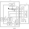
- FIG. 2 is a schematic structural diagram of a charging protection apparatus according to an embodiment of the present invention.
- a charging protection apparatus 1 includes: a charging management unit 10, a voltage detection unit 11, a temperature detection unit 12, a current detection unit 13, a temperature sensor 14, and a micro USB interface 15.
- a charged device is connected to a built-in micro USB interface 20 of a charger 2 by using the built-in micro USB interface 15.
- the voltage detection unit 11 is connected to a D+ pin, a D- pin, and an ID pin of the micro USB interface 15, and is configured to detect whether a voltage on the D+ pin, the D- pin, or the ID pin falls beyond a preset voltage range.
- the current detection unit 13 is connected to a VBUS pin of the micro USB interface 15, and is configured to detect whether a current on the VBUS pin is less than a preset current threshold.
- the temperature detection unit 12 is connected to the temperature sensor 14, and is configured to obtain a temperature measured by the temperature sensor 14, and detect, according to the obtained temperature, whether a temperature rise of the micro USB interface 15 is greater than a preset temperature rise threshold, where the temperature sensor is disposed near the micro USB interface 15.
- the charging management unit 10 is separately connected to the voltage detection unit 11, the current detection unit 13, and the temperature detection unit 12, and is configured to disconnect a charging circuit of the charger 2 when a detection result of one or more of the voltage detection unit 11, the current detection unit 13, or the temperature detection unit 12 is yes.
- the charger 2 includes the micro USB interface 20 and a power management chip 21.
- the micro USB interface 20 of the charger 2 and the micro USB interface 15 of the charged device are mutually mated. As shown in FIG. 3 , the micro USB interface 15 is a female connector, and the micro USB interface 20 is a male connector.
- the temperature sensor 14 is disposed near the micro USB interface 15.
- a method by which the charging protection apparatus 1 disconnects the charging circuit of the charger 2 may be: disconnecting the charging circuit of the charger 2 on a charged device side, or instructing the charger to disconnect the local charging circuit. After disconnecting the charging circuit, the charging protection apparatus 1 sends the charged device a notification indicating that a charging exception occurs. After receiving the notification, the charged device displays, on a display screen, text information indicating that a charging exception occurs, and also adjusts a volume to the highest and outputs a voice prompt by using a speaker.
- the charging management unit 10 is further configured to: send instruction information to the charger 2 by using the D+ pin and the D- pin, where the instruction information is used to instruct the charger 2 to disconnect the charging circuit.
- the charging protection apparatus 1 further includes a MOS transistor Q and a diode D, where a gate of the MOS transistor Q is connected to the charging management unit 10, a drain of the MOS transistor Q is grounded, a source of the MOS transistor Q is connected to the VBUS pin of the micro USB interface 15, a cathode of the diode D is connected to the drain of the MOS transistor Q, and an anode of the diode D is connected to the source of the MOS transistor.
- the charging management unit 10 loads a turn-on voltage by using the gate of the MOS transistor Q, to ground power output that is transmitted on the VBUS pin by the charger 2. In this way, charging power of the charger 2 is not loaded to the charged device.
- the charging protection apparatus 1 further include a capacitor C, where one terminal of the capacitor is connected to the VBUS pin, and another terminal of the capacitor is grounded.
- the charging management unit 10 is further configured to: send alarm prompt information to the charged device, where the alarm prompt information is used to instruct the charged device to use a display device to display text information indicating that a charging exception occurs on the charged device, and instruct the charged device to use an audio apparatus to output audio information indicating that a charging exception occurs on the charged device.
- the charging protection apparatus 1 may be located in the charged device and is a part of the charged device; or the charging protection apparatus and the charged device may be independent from each other, which is not limited in the present invention.
- the program may be stored in a computer readable storage medium. When the program runs, the processes of the methods in the embodiments are performed.
- the foregoing storage medium may include: a magnetic disk, an optical disc, a read-only memory (Read-Only Memory, ROM), or a random access memory (Random Access Memory, RAM).
Landscapes
- Engineering & Computer Science (AREA)
- Power Engineering (AREA)
- Business, Economics & Management (AREA)
- Emergency Management (AREA)
- Physics & Mathematics (AREA)
- General Physics & Mathematics (AREA)
- Charge And Discharge Circuits For Batteries Or The Like (AREA)
- Protection Of Static Devices (AREA)
- Power Sources (AREA)
Applications Claiming Priority (1)
| Application Number | Priority Date | Filing Date | Title |
|---|---|---|---|
| PCT/CN2014/095733 WO2016106616A1 (fr) | 2014-12-31 | 2014-12-31 | Procédé et appareil de protection de charge |
Publications (3)
| Publication Number | Publication Date |
|---|---|
| EP3211740A1 true EP3211740A1 (fr) | 2017-08-30 |
| EP3211740A4 EP3211740A4 (fr) | 2018-03-28 |
| EP3211740B1 EP3211740B1 (fr) | 2019-12-11 |
Family
ID=56283891
Family Applications (1)
| Application Number | Title | Priority Date | Filing Date |
|---|---|---|---|
| EP14909425.2A Active EP3211740B1 (fr) | 2014-12-31 | 2014-12-31 | Procédé et appareil de protection de charge |
Country Status (12)
| Country | Link |
|---|---|
| US (2) | US10250048B2 (fr) |
| EP (1) | EP3211740B1 (fr) |
| JP (1) | JP6388357B2 (fr) |
| KR (1) | KR102085684B1 (fr) |
| CN (2) | CN110571759B (fr) |
| AU (1) | AU2014415910B2 (fr) |
| BR (1) | BR112017011439B1 (fr) |
| CA (1) | CA2969011C (fr) |
| ES (1) | ES2771901T3 (fr) |
| RU (1) | RU2677252C1 (fr) |
| SG (1) | SG11201704195PA (fr) |
| WO (1) | WO2016106616A1 (fr) |
Cited By (3)
| Publication number | Priority date | Publication date | Assignee | Title |
|---|---|---|---|---|
| EP3522332A4 (fr) * | 2016-10-14 | 2019-09-25 | Huawei Technologies Co., Ltd. | Chargeur |
| WO2020091604A1 (fr) * | 2018-10-29 | 2020-05-07 | Nordic Itech As | Dispositif de sécurité et son procédé d'utilisation |
| EP3920362A4 (fr) * | 2019-01-31 | 2022-03-30 | Vivo Mobile Communication Co., Ltd. | Circuit de charge et dispositif électronique |
Families Citing this family (34)
| Publication number | Priority date | Publication date | Assignee | Title |
|---|---|---|---|---|
| SG11201704195PA (en) * | 2014-12-31 | 2017-06-29 | Huawei Tech Co Ltd | Charging protection method and apparatus |
| KR101894777B1 (ko) * | 2015-09-22 | 2018-09-04 | 광동 오포 모바일 텔레커뮤니케이션즈 코포레이션 리미티드 | 충전 제어 방법과 장치 및 전자 기기 |
| CN106537724B (zh) * | 2016-02-05 | 2020-01-10 | Oppo广东移动通信有限公司 | 充电方法、适配器和移动终端 |
| JP6838879B2 (ja) * | 2016-07-13 | 2021-03-03 | ローム株式会社 | 受電装置およびその制御回路、電子機器、給電システムの動作方法 |
| EP3276811B1 (fr) | 2016-07-26 | 2019-03-06 | Guangdong Oppo Mobile Telecommunications Corp., Ltd. | Système de recharge, procédé de recharge et adaptateur de puissance |
| WO2018032274A1 (fr) * | 2016-08-15 | 2018-02-22 | 北京小米移动软件有限公司 | Dispositif électronique, chargeur, et système et procédé de charge |
| EP3503332A4 (fr) | 2016-08-29 | 2019-08-21 | Huawei Technologies Co., Ltd. | Procédé de protection pendant une recharge électrique, terminal et chargeur |
| JP6144809B1 (ja) * | 2016-09-05 | 2017-06-07 | ホシデン株式会社 | 電源装置 |
| CN112803539B (zh) * | 2016-11-15 | 2023-09-08 | 华为技术有限公司 | 一种充电方法及相关设备 |
| US10289477B2 (en) * | 2017-02-27 | 2019-05-14 | Semiconductor Components Industries, Llc | USB electronic marker circuit and method therefor |
| KR102325888B1 (ko) * | 2017-03-28 | 2021-11-12 | 삼성전자주식회사 | 전자 장치 및 전자 장치의 수분 감지 방법 |
| KR102439078B1 (ko) * | 2017-06-23 | 2022-09-01 | 삼성전자주식회사 | 전자 장치 및 그의 충전 제어 방법 |
| CN107590962B (zh) * | 2017-08-30 | 2020-07-17 | 安徽三禾一信息科技有限公司 | 一种报警方法及终端 |
| CN107831386A (zh) * | 2017-10-31 | 2018-03-23 | 奇酷互联网络科技(深圳)有限公司 | 识别充电异常的方法、设备、移动终端和计算机存储介质 |
| CN108054795B (zh) * | 2017-12-15 | 2021-09-17 | 华勤技术股份有限公司 | 终端及充电方法 |
| CN108279370B (zh) * | 2018-01-23 | 2020-05-05 | 维沃移动通信有限公司 | 一种外部电容器异常检测方法、半压充电电路及移动终端 |
| CN109378877B (zh) * | 2018-11-13 | 2022-02-01 | Oppo(重庆)智能科技有限公司 | 充电电路、充电处理方法、电子设备及存储介质 |
| CN110892278B (zh) * | 2018-11-14 | 2022-01-11 | Oppo广东移动通信有限公司 | 电子设备的故障验证方法及系统 |
| US11362528B2 (en) | 2019-06-20 | 2022-06-14 | Microsoft Technology Licensing, Llc | Mitigation of audible output in a charging circuit |
| CN110138056B (zh) * | 2019-06-27 | 2021-08-17 | 深圳莱福德科技股份有限公司 | 应急电源保护方法和装置 |
| CN110635537B (zh) * | 2019-10-14 | 2022-02-08 | 北京云迹科技有限公司 | 充电控制方法、装置及机器人 |
| CN113765165A (zh) * | 2020-06-03 | 2021-12-07 | 北京小米移动软件有限公司 | 充电接口及充电接口的保护方法、保护装置及存储介质 |
| KR102647600B1 (ko) * | 2021-05-21 | 2024-03-14 | 세기전자산업(주) | 충전기 관리시스템 |
| CN113300447B (zh) * | 2021-06-18 | 2023-05-05 | 新乡北方车辆仪表有限公司 | 一种高压超级电容模组的自适应充电方法 |
| CN114256926A (zh) * | 2021-12-22 | 2022-03-29 | 北京智充科技有限公司 | 基于温度变化的车辆充电方法、装置、设备及存储介质 |
| CN114624569A (zh) * | 2022-03-04 | 2022-06-14 | 惠州Tcl移动通信有限公司 | 传感器电路异常检测方法、电路、装置、智能设备及介质 |
| CN116979625A (zh) * | 2022-03-29 | 2023-10-31 | 中兴通讯股份有限公司 | 充电保护电路、充电保护方法、终端设备及存储介质 |
| US11588216B1 (en) * | 2022-05-24 | 2023-02-21 | Inventus Power, Inc. | Detecting conducting fluids in external connectors of conformable wearable battery packs using unused pins |
| EP4533111A4 (fr) * | 2022-05-24 | 2026-05-20 | Inventus Power Inc | Détection de fluides conducteurs dans des connecteurs externes |
| US11777237B1 (en) * | 2022-05-24 | 2023-10-03 | Inventus Power, Inc. | Disconnecting power from external USB connectors of conformable wearable battery packs in the presence of conducting fluids |
| CN115042655A (zh) * | 2022-07-07 | 2022-09-13 | 国网上海市电力公司 | 一种电动船舶直流充电接口安全防护方法、装置及系统 |
| JP2025535647A (ja) * | 2022-09-21 | 2025-10-28 | グーグル エルエルシー | 電子デバイスの充電インターフェースでの微細な短絡の検出 |
| CN117081205A (zh) * | 2023-08-21 | 2023-11-17 | 昆山迈致治具科技有限公司 | 多路快充控制电路和方法、充电芯片以及供电设备 |
| US20260112912A1 (en) * | 2024-10-17 | 2026-04-23 | Qorvo Us, Inc. | Cable failure protection and battery kickstart in an electronic device |
Family Cites Families (38)
| Publication number | Priority date | Publication date | Assignee | Title |
|---|---|---|---|---|
| US2585005A (en) * | 1949-10-26 | 1952-02-12 | Sterlingworth Company | Method and apparatus for charging batteries |
| US6518726B1 (en) | 2002-01-18 | 2003-02-11 | Eagle-Picher Technologies, L.L.C. | Battery charger and charge control system |
| US6819083B1 (en) | 2003-04-25 | 2004-11-16 | Motorola, Inc. | Dual use thermistor for battery cell thermal protection and battery pack overcharge/undercharge protection |
| JP2007214420A (ja) | 2006-02-10 | 2007-08-23 | Matsushita Electric Ind Co Ltd | 半導体集積回路 |
| US7902794B2 (en) | 2007-07-03 | 2011-03-08 | Intersil Americas Inc. | Over-voltage protected battery charger with bypass |
| US7859226B2 (en) * | 2007-07-17 | 2010-12-28 | Tdk-Lambda Corporation | Method and device for safety protection of secondary battery |
| JP5217468B2 (ja) | 2008-02-01 | 2013-06-19 | 株式会社リコー | 二次電池保護用半導体装置および該二次電池保護用半導体装置を用いた電池パック、ならびに該電池パックを用いた電子機器 |
| CN102106053A (zh) | 2008-04-25 | 2011-06-22 | 捷通国际有限公司 | 输入保护电路 |
| JP5329840B2 (ja) * | 2008-05-23 | 2013-10-30 | ローム株式会社 | 過電圧保護回路ならびにそれを用いた電源管理回路および電子機器 |
| JP2010208200A (ja) * | 2009-03-11 | 2010-09-24 | Fuji Xerox Co Ltd | 画像形成装置およびプログラム |
| JP2010259254A (ja) * | 2009-04-27 | 2010-11-11 | Panasonic Corp | 電流制御装置及び保護装置 |
| CN101567556B (zh) | 2009-05-26 | 2012-12-05 | 上海华勤通讯技术有限公司 | 用于手机充电的过压充电保护装置及方法 |
| JP5303814B2 (ja) * | 2009-06-29 | 2013-10-02 | オンキヨー株式会社 | 電子機器及びアダプタ装置 |
| CN201821092U (zh) | 2010-10-21 | 2011-05-04 | 天津光电通信技术有限公司 | 锂动力电池组保护电路 |
| CN102570403B (zh) * | 2010-12-28 | 2015-04-22 | 宁波良业电器有限公司 | 锂电池充电放电的温度保护电路 |
| JP5711040B2 (ja) * | 2011-04-28 | 2015-04-30 | トランスフォーム・ジャパン株式会社 | 双方向スイッチおよびそれを利用した充放電保護装置 |
| CN202309997U (zh) * | 2011-10-27 | 2012-07-04 | 康佳集团股份有限公司 | 可以给接入设备充电的机顶盒 |
| JP6099894B2 (ja) * | 2012-07-11 | 2017-03-22 | セミコンダクター・コンポーネンツ・インダストリーズ・リミテッド・ライアビリティ・カンパニー | 携帯電子機器の充電システム |
| CN202840602U (zh) * | 2012-07-27 | 2013-03-27 | 深圳市显盈电子科技有限公司 | Usb智能充电器 |
| WO2014077978A1 (fr) * | 2012-11-14 | 2014-05-22 | Apple Inc. | Charge haute tension pour un dispositif portable |
| JP6101493B2 (ja) * | 2013-01-15 | 2017-03-22 | ローム株式会社 | 電力供給装置、acアダプタ、電子機器および電力供給システム |
| CN203434605U (zh) * | 2013-06-17 | 2014-02-12 | 苏州天趣信息科技有限公司 | 过充电保护装置 |
| CN104078943B (zh) * | 2013-06-17 | 2017-08-25 | 惠州市兴飞技术有限公司 | 过充电保护装置及防止手机过充电的方法 |
| CN104242365B (zh) * | 2013-06-19 | 2019-01-04 | 深圳富泰宏精密工业有限公司 | 便携式电子装置及使用方法 |
| JP5447723B1 (ja) | 2013-07-19 | 2014-03-19 | パナソニック株式会社 | 充電器及び電子機器システム |
| CN203368107U (zh) | 2013-08-09 | 2013-12-25 | 向智勇 | 具有过压过流保护的充电器 |
| CN203491732U (zh) * | 2013-08-13 | 2014-03-19 | 中兴通讯股份有限公司 | 一种移动终端充电器 |
| CN203398772U (zh) | 2013-08-27 | 2014-01-15 | 武汉大学苏州研究院 | 一种多节锂电池保护系统 |
| CN103545882B (zh) | 2013-10-11 | 2015-07-22 | 华为技术有限公司 | 电池在位检测方法、装置及充电系统 |
| CN103545889B (zh) * | 2013-10-25 | 2016-05-11 | Tcl通讯(宁波)有限公司 | Usb充电系统、充电器、移动终端和充电控制方法 |
| CN103545803B (zh) * | 2013-10-31 | 2016-08-17 | 广东威创视讯科技股份有限公司 | 设备电源接口电路保护装置 |
| CN203722280U (zh) * | 2013-12-23 | 2014-07-16 | 阿特斯(中国)投资有限公司 | 一种太阳能usb充电装置 |
| CN203761085U (zh) | 2014-01-24 | 2014-08-06 | 上海智驰电子科技发展有限公司 | 具有过压、欠压、过流、过温保护功能的移动电源 |
| WO2015113463A1 (fr) * | 2014-01-28 | 2015-08-06 | 广东欧珀移动通信有限公司 | Adaptateur d'alimentation, terminal et procédé de traitement d'exception d'impédance de boucle de charge |
| CN103779907B (zh) | 2014-01-28 | 2016-11-23 | 广东欧珀移动通信有限公司 | 终端及其电池充电控制装置与方法 |
| CN203883502U (zh) * | 2014-03-24 | 2014-10-15 | 西安乾易企业管理咨询有限公司 | 一种可快速充电的电源适配器 |
| SG11201704195PA (en) * | 2014-12-31 | 2017-06-29 | Huawei Tech Co Ltd | Charging protection method and apparatus |
| US20160308386A1 (en) * | 2015-03-13 | 2016-10-20 | IMHear Corporation | Rechargeable hearing aid and charging system therefor |
-
2014
- 2014-12-31 SG SG11201704195PA patent/SG11201704195PA/en unknown
- 2014-12-31 WO PCT/CN2014/095733 patent/WO2016106616A1/fr not_active Ceased
- 2014-12-31 CA CA2969011A patent/CA2969011C/fr active Active
- 2014-12-31 AU AU2014415910A patent/AU2014415910B2/en active Active
- 2014-12-31 BR BR112017011439-9A patent/BR112017011439B1/pt active IP Right Grant
- 2014-12-31 US US15/532,026 patent/US10250048B2/en active Active
- 2014-12-31 CN CN201910833918.7A patent/CN110571759B/zh active Active
- 2014-12-31 CN CN201480084435.7A patent/CN107112743B/zh active Active
- 2014-12-31 EP EP14909425.2A patent/EP3211740B1/fr active Active
- 2014-12-31 ES ES14909425T patent/ES2771901T3/es active Active
- 2014-12-31 KR KR1020177016588A patent/KR102085684B1/ko active Active
- 2014-12-31 RU RU2017124241A patent/RU2677252C1/ru active
- 2014-12-31 JP JP2017533281A patent/JP6388357B2/ja active Active
-
2019
- 2019-02-01 US US16/265,609 patent/US10778018B2/en active Active
Cited By (4)
| Publication number | Priority date | Publication date | Assignee | Title |
|---|---|---|---|---|
| EP3522332A4 (fr) * | 2016-10-14 | 2019-09-25 | Huawei Technologies Co., Ltd. | Chargeur |
| WO2020091604A1 (fr) * | 2018-10-29 | 2020-05-07 | Nordic Itech As | Dispositif de sécurité et son procédé d'utilisation |
| EP3920362A4 (fr) * | 2019-01-31 | 2022-03-30 | Vivo Mobile Communication Co., Ltd. | Circuit de charge et dispositif électronique |
| US12046932B2 (en) | 2019-01-31 | 2024-07-23 | Vivo Mobile Communication Co., Ltd. | Charging circuit and electronic device |
Also Published As
| Publication number | Publication date |
|---|---|
| CA2969011A1 (fr) | 2016-07-07 |
| KR102085684B1 (ko) | 2020-03-06 |
| CN107112743B (zh) | 2019-10-01 |
| US20190165588A1 (en) | 2019-05-30 |
| ES2771901T3 (es) | 2020-07-07 |
| JP2018501762A (ja) | 2018-01-18 |
| US10250048B2 (en) | 2019-04-02 |
| RU2677252C1 (ru) | 2019-01-16 |
| WO2016106616A1 (fr) | 2016-07-07 |
| CN107112743A (zh) | 2017-08-29 |
| AU2014415910A1 (en) | 2017-06-15 |
| EP3211740B1 (fr) | 2019-12-11 |
| US10778018B2 (en) | 2020-09-15 |
| AU2014415910B2 (en) | 2019-06-06 |
| BR112017011439B1 (pt) | 2022-05-03 |
| CN110571759A (zh) | 2019-12-13 |
| CN110571759B (zh) | 2021-12-21 |
| SG11201704195PA (en) | 2017-06-29 |
| EP3211740A4 (fr) | 2018-03-28 |
| KR20170084306A (ko) | 2017-07-19 |
| JP6388357B2 (ja) | 2018-09-12 |
| US20170271897A1 (en) | 2017-09-21 |
| CA2969011C (fr) | 2019-09-17 |
| BR112017011439A2 (pt) | 2018-04-03 |
Similar Documents
| Publication | Publication Date | Title |
|---|---|---|
| US10778018B2 (en) | Charging protection method and apparatus | |
| US11631981B2 (en) | Power adapter, terminal, and method for processing impedance anomalies in charging loop | |
| US10181742B2 (en) | Electronic device, charger within the electronic device, and detecting method for detecting abnormal status of connector of electronic device | |
| US10658860B2 (en) | Electronic device, charger within the electronic device, and detecting method for detecting abnormal status of connector of electronic device | |
| US9859726B2 (en) | Detection circuit and method for starting charging | |
| CN107834657B (zh) | 一种充电方法、终端设备及电源适配器 | |
| WO2015113465A1 (fr) | Terminal, adaptateur d'alimentation et procédé de traitement d'exception de charge | |
| CN106374577A (zh) | 一种充电保护方法和装置 | |
| WO2020088388A1 (fr) | Circuit de commande de charge, circuit de charge et procédé de commande de charge | |
| CN106707194B (zh) | 一种充电电池检测方法及电子设备 | |
| CN106849246A (zh) | 充电接口短路检测装置、移动终端及短路检测方法 | |
| CN107171373A (zh) | 电池保护方法及装置、终端 | |
| CN105553049B (zh) | 充电操作控制方法及装置 | |
| CN110783984B (zh) | 充电盒及其充电控制方法、可读存储介质 | |
| CN106207298A (zh) | 一种充电方法和用户设备 | |
| CN107069128A (zh) | 一种在充电状态下断开充电的方法及装置 |
Legal Events
| Date | Code | Title | Description |
|---|---|---|---|
| STAA | Information on the status of an ep patent application or granted ep patent |
Free format text: STATUS: THE INTERNATIONAL PUBLICATION HAS BEEN MADE |
|
| PUAI | Public reference made under article 153(3) epc to a published international application that has entered the european phase |
Free format text: ORIGINAL CODE: 0009012 |
|
| STAA | Information on the status of an ep patent application or granted ep patent |
Free format text: STATUS: REQUEST FOR EXAMINATION WAS MADE |
|
| 17P | Request for examination filed |
Effective date: 20170522 |
|
| AK | Designated contracting states |
Kind code of ref document: A1 Designated state(s): AL AT BE BG CH CY CZ DE DK EE ES FI FR GB GR HR HU IE IS IT LI LT LU LV MC MK MT NL NO PL PT RO RS SE SI SK SM TR |
|
| AX | Request for extension of the european patent |
Extension state: BA ME |
|
| A4 | Supplementary search report drawn up and despatched |
Effective date: 20180223 |
|
| RIC1 | Information provided on ipc code assigned before grant |
Ipc: H02H 5/04 20060101ALI20180219BHEP Ipc: H02H 7/18 20060101AFI20180219BHEP Ipc: H02J 7/00 20060101ALI20180219BHEP Ipc: H02J 7/04 20060101ALI20180219BHEP |
|
| DAX | Request for extension of the european patent (deleted) | ||
| STAA | Information on the status of an ep patent application or granted ep patent |
Free format text: STATUS: EXAMINATION IS IN PROGRESS |
|
| 17Q | First examination report despatched |
Effective date: 20190124 |
|
| GRAP | Despatch of communication of intention to grant a patent |
Free format text: ORIGINAL CODE: EPIDOSNIGR1 |
|
| STAA | Information on the status of an ep patent application or granted ep patent |
Free format text: STATUS: GRANT OF PATENT IS INTENDED |
|
| INTG | Intention to grant announced |
Effective date: 20190705 |
|
| GRAS | Grant fee paid |
Free format text: ORIGINAL CODE: EPIDOSNIGR3 |
|
| GRAA | (expected) grant |
Free format text: ORIGINAL CODE: 0009210 |
|
| STAA | Information on the status of an ep patent application or granted ep patent |
Free format text: STATUS: THE PATENT HAS BEEN GRANTED |
|
| AK | Designated contracting states |
Kind code of ref document: B1 Designated state(s): AL AT BE BG CH CY CZ DE DK EE ES FI FR GB GR HR HU IE IS IT LI LT LU LV MC MK MT NL NO PL PT RO RS SE SI SK SM TR |
|
| REG | Reference to a national code |
Ref country code: GB Ref legal event code: FG4D |
|
| REG | Reference to a national code |
Ref country code: CH Ref legal event code: EP |
|
| REG | Reference to a national code |
Ref country code: AT Ref legal event code: REF Ref document number: 1213140 Country of ref document: AT Kind code of ref document: T Effective date: 20191215 |
|
| REG | Reference to a national code |
Ref country code: DE Ref legal event code: R096 Ref document number: 602014058438 Country of ref document: DE |
|
| REG | Reference to a national code |
Ref country code: IE Ref legal event code: FG4D |
|
| REG | Reference to a national code |
Ref country code: NL Ref legal event code: FP |
|
| REG | Reference to a national code |
Ref country code: LT Ref legal event code: MG4D |
|
| PG25 | Lapsed in a contracting state [announced via postgrant information from national office to epo] |
Ref country code: NO Free format text: LAPSE BECAUSE OF FAILURE TO SUBMIT A TRANSLATION OF THE DESCRIPTION OR TO PAY THE FEE WITHIN THE PRESCRIBED TIME-LIMIT Effective date: 20200311 Ref country code: LT Free format text: LAPSE BECAUSE OF FAILURE TO SUBMIT A TRANSLATION OF THE DESCRIPTION OR TO PAY THE FEE WITHIN THE PRESCRIBED TIME-LIMIT Effective date: 20191211 Ref country code: GR Free format text: LAPSE BECAUSE OF FAILURE TO SUBMIT A TRANSLATION OF THE DESCRIPTION OR TO PAY THE FEE WITHIN THE PRESCRIBED TIME-LIMIT Effective date: 20200312 Ref country code: LV Free format text: LAPSE BECAUSE OF FAILURE TO SUBMIT A TRANSLATION OF THE DESCRIPTION OR TO PAY THE FEE WITHIN THE PRESCRIBED TIME-LIMIT Effective date: 20191211 Ref country code: FI Free format text: LAPSE BECAUSE OF FAILURE TO SUBMIT A TRANSLATION OF THE DESCRIPTION OR TO PAY THE FEE WITHIN THE PRESCRIBED TIME-LIMIT Effective date: 20191211 Ref country code: BG Free format text: LAPSE BECAUSE OF FAILURE TO SUBMIT A TRANSLATION OF THE DESCRIPTION OR TO PAY THE FEE WITHIN THE PRESCRIBED TIME-LIMIT Effective date: 20200311 Ref country code: SE Free format text: LAPSE BECAUSE OF FAILURE TO SUBMIT A TRANSLATION OF THE DESCRIPTION OR TO PAY THE FEE WITHIN THE PRESCRIBED TIME-LIMIT Effective date: 20191211 |
|
| PG25 | Lapsed in a contracting state [announced via postgrant information from national office to epo] |
Ref country code: HR Free format text: LAPSE BECAUSE OF FAILURE TO SUBMIT A TRANSLATION OF THE DESCRIPTION OR TO PAY THE FEE WITHIN THE PRESCRIBED TIME-LIMIT Effective date: 20191211 Ref country code: RS Free format text: LAPSE BECAUSE OF FAILURE TO SUBMIT A TRANSLATION OF THE DESCRIPTION OR TO PAY THE FEE WITHIN THE PRESCRIBED TIME-LIMIT Effective date: 20191211 |
|
| PG25 | Lapsed in a contracting state [announced via postgrant information from national office to epo] |
Ref country code: AL Free format text: LAPSE BECAUSE OF FAILURE TO SUBMIT A TRANSLATION OF THE DESCRIPTION OR TO PAY THE FEE WITHIN THE PRESCRIBED TIME-LIMIT Effective date: 20191211 |
|
| REG | Reference to a national code |
Ref country code: ES Ref legal event code: FG2A Ref document number: 2771901 Country of ref document: ES Kind code of ref document: T3 Effective date: 20200707 |
|
| PG25 | Lapsed in a contracting state [announced via postgrant information from national office to epo] |
Ref country code: CZ Free format text: LAPSE BECAUSE OF FAILURE TO SUBMIT A TRANSLATION OF THE DESCRIPTION OR TO PAY THE FEE WITHIN THE PRESCRIBED TIME-LIMIT Effective date: 20191211 Ref country code: RO Free format text: LAPSE BECAUSE OF FAILURE TO SUBMIT A TRANSLATION OF THE DESCRIPTION OR TO PAY THE FEE WITHIN THE PRESCRIBED TIME-LIMIT Effective date: 20191211 Ref country code: EE Free format text: LAPSE BECAUSE OF FAILURE TO SUBMIT A TRANSLATION OF THE DESCRIPTION OR TO PAY THE FEE WITHIN THE PRESCRIBED TIME-LIMIT Effective date: 20191211 Ref country code: PT Free format text: LAPSE BECAUSE OF FAILURE TO SUBMIT A TRANSLATION OF THE DESCRIPTION OR TO PAY THE FEE WITHIN THE PRESCRIBED TIME-LIMIT Effective date: 20200506 |
|
| REG | Reference to a national code |
Ref country code: CH Ref legal event code: PL |
|
| REG | Reference to a national code |
Ref country code: BE Ref legal event code: MM Effective date: 20191231 |
|
| PG25 | Lapsed in a contracting state [announced via postgrant information from national office to epo] |
Ref country code: SM Free format text: LAPSE BECAUSE OF FAILURE TO SUBMIT A TRANSLATION OF THE DESCRIPTION OR TO PAY THE FEE WITHIN THE PRESCRIBED TIME-LIMIT Effective date: 20191211 Ref country code: SK Free format text: LAPSE BECAUSE OF FAILURE TO SUBMIT A TRANSLATION OF THE DESCRIPTION OR TO PAY THE FEE WITHIN THE PRESCRIBED TIME-LIMIT Effective date: 20191211 Ref country code: IS Free format text: LAPSE BECAUSE OF FAILURE TO SUBMIT A TRANSLATION OF THE DESCRIPTION OR TO PAY THE FEE WITHIN THE PRESCRIBED TIME-LIMIT Effective date: 20200411 |
|
| REG | Reference to a national code |
Ref country code: DE Ref legal event code: R097 Ref document number: 602014058438 Country of ref document: DE |
|
| PG25 | Lapsed in a contracting state [announced via postgrant information from national office to epo] |
Ref country code: MC Free format text: LAPSE BECAUSE OF FAILURE TO SUBMIT A TRANSLATION OF THE DESCRIPTION OR TO PAY THE FEE WITHIN THE PRESCRIBED TIME-LIMIT Effective date: 20191211 |
|
| REG | Reference to a national code |
Ref country code: AT Ref legal event code: MK05 Ref document number: 1213140 Country of ref document: AT Kind code of ref document: T Effective date: 20191211 |
|
| PLBE | No opposition filed within time limit |
Free format text: ORIGINAL CODE: 0009261 |
|
| STAA | Information on the status of an ep patent application or granted ep patent |
Free format text: STATUS: NO OPPOSITION FILED WITHIN TIME LIMIT |
|
| PG25 | Lapsed in a contracting state [announced via postgrant information from national office to epo] |
Ref country code: LU Free format text: LAPSE BECAUSE OF NON-PAYMENT OF DUE FEES Effective date: 20191231 Ref country code: IE Free format text: LAPSE BECAUSE OF NON-PAYMENT OF DUE FEES Effective date: 20191231 Ref country code: DK Free format text: LAPSE BECAUSE OF FAILURE TO SUBMIT A TRANSLATION OF THE DESCRIPTION OR TO PAY THE FEE WITHIN THE PRESCRIBED TIME-LIMIT Effective date: 20191211 |
|
| 26N | No opposition filed |
Effective date: 20200914 |
|
| PG25 | Lapsed in a contracting state [announced via postgrant information from national office to epo] |
Ref country code: AT Free format text: LAPSE BECAUSE OF FAILURE TO SUBMIT A TRANSLATION OF THE DESCRIPTION OR TO PAY THE FEE WITHIN THE PRESCRIBED TIME-LIMIT Effective date: 20191211 Ref country code: LI Free format text: LAPSE BECAUSE OF NON-PAYMENT OF DUE FEES Effective date: 20191231 Ref country code: CH Free format text: LAPSE BECAUSE OF NON-PAYMENT OF DUE FEES Effective date: 20191231 Ref country code: BE Free format text: LAPSE BECAUSE OF NON-PAYMENT OF DUE FEES Effective date: 20191231 Ref country code: SI Free format text: LAPSE BECAUSE OF FAILURE TO SUBMIT A TRANSLATION OF THE DESCRIPTION OR TO PAY THE FEE WITHIN THE PRESCRIBED TIME-LIMIT Effective date: 20191211 |
|
| PG25 | Lapsed in a contracting state [announced via postgrant information from national office to epo] |
Ref country code: IT Free format text: LAPSE BECAUSE OF FAILURE TO SUBMIT A TRANSLATION OF THE DESCRIPTION OR TO PAY THE FEE WITHIN THE PRESCRIBED TIME-LIMIT Effective date: 20191211 |
|
| PG25 | Lapsed in a contracting state [announced via postgrant information from national office to epo] |
Ref country code: PL Free format text: LAPSE BECAUSE OF FAILURE TO SUBMIT A TRANSLATION OF THE DESCRIPTION OR TO PAY THE FEE WITHIN THE PRESCRIBED TIME-LIMIT Effective date: 20191211 |
|
| PG25 | Lapsed in a contracting state [announced via postgrant information from national office to epo] |
Ref country code: CY Free format text: LAPSE BECAUSE OF FAILURE TO SUBMIT A TRANSLATION OF THE DESCRIPTION OR TO PAY THE FEE WITHIN THE PRESCRIBED TIME-LIMIT Effective date: 20191211 |
|
| PG25 | Lapsed in a contracting state [announced via postgrant information from national office to epo] |
Ref country code: MT Free format text: LAPSE BECAUSE OF FAILURE TO SUBMIT A TRANSLATION OF THE DESCRIPTION OR TO PAY THE FEE WITHIN THE PRESCRIBED TIME-LIMIT Effective date: 20191211 Ref country code: HU Free format text: LAPSE BECAUSE OF FAILURE TO SUBMIT A TRANSLATION OF THE DESCRIPTION OR TO PAY THE FEE WITHIN THE PRESCRIBED TIME-LIMIT; INVALID AB INITIO Effective date: 20141231 |
|
| PG25 | Lapsed in a contracting state [announced via postgrant information from national office to epo] |
Ref country code: TR Free format text: LAPSE BECAUSE OF FAILURE TO SUBMIT A TRANSLATION OF THE DESCRIPTION OR TO PAY THE FEE WITHIN THE PRESCRIBED TIME-LIMIT Effective date: 20191211 |
|
| PG25 | Lapsed in a contracting state [announced via postgrant information from national office to epo] |
Ref country code: MK Free format text: LAPSE BECAUSE OF FAILURE TO SUBMIT A TRANSLATION OF THE DESCRIPTION OR TO PAY THE FEE WITHIN THE PRESCRIBED TIME-LIMIT Effective date: 20191211 |
|
| P01 | Opt-out of the competence of the unified patent court (upc) registered |
Effective date: 20230510 |
|
| PGFP | Annual fee paid to national office [announced via postgrant information from national office to epo] |
Ref country code: NL Payment date: 20251112 Year of fee payment: 12 |
|
| PGFP | Annual fee paid to national office [announced via postgrant information from national office to epo] |
Ref country code: DE Payment date: 20251104 Year of fee payment: 12 |
|
| PGFP | Annual fee paid to national office [announced via postgrant information from national office to epo] |
Ref country code: GB Payment date: 20251114 Year of fee payment: 12 |
|
| PGFP | Annual fee paid to national office [announced via postgrant information from national office to epo] |
Ref country code: FR Payment date: 20251110 Year of fee payment: 12 |
|
| PGFP | Annual fee paid to national office [announced via postgrant information from national office to epo] |
Ref country code: ES Payment date: 20260112 Year of fee payment: 12 |