EP3211781A1 - Spectroscope de masse - Google Patents
Spectroscope de masse Download PDFInfo
- Publication number
- EP3211781A1 EP3211781A1 EP14904426.5A EP14904426A EP3211781A1 EP 3211781 A1 EP3211781 A1 EP 3211781A1 EP 14904426 A EP14904426 A EP 14904426A EP 3211781 A1 EP3211781 A1 EP 3211781A1
- Authority
- EP
- European Patent Office
- Prior art keywords
- voltage
- positive
- negative
- section
- voltage generation
- Prior art date
- Legal status (The legal status is an assumption and is not a legal conclusion. Google has not performed a legal analysis and makes no representation as to the accuracy of the status listed.)
- Withdrawn
Links
Images


Classifications
-
- H—ELECTRICITY
- H01—ELECTRIC ELEMENTS
- H01J—ELECTRIC DISCHARGE TUBES OR DISCHARGE LAMPS
- H01J49/00—Particle spectrometers or separator tubes
- H01J49/02—Details
- H01J49/022—Circuit arrangements, e.g. for generating deviation currents or voltages ; Components associated with high voltage supply
-
- H—ELECTRICITY
- H01—ELECTRIC ELEMENTS
- H01J—ELECTRIC DISCHARGE TUBES OR DISCHARGE LAMPS
- H01J3/00—Details of electron-optical or ion-optical arrangements common to two or more basic types of discharge tubes or lamps
- H01J3/40—Arrangements for removing or diverting unwanted particles, e.g. for negative ions or fringing electrons; Arrangements for velocity or mass selection
-
- H—ELECTRICITY
- H01—ELECTRIC ELEMENTS
- H01J—ELECTRIC DISCHARGE TUBES OR DISCHARGE LAMPS
- H01J49/00—Particle spectrometers or separator tubes
- H01J49/0027—Methods for using particle spectrometers
- H01J49/0036—Step by step routines describing the handling of the data generated during a measurement
-
- H—ELECTRICITY
- H01—ELECTRIC ELEMENTS
- H01J—ELECTRIC DISCHARGE TUBES OR DISCHARGE LAMPS
- H01J49/00—Particle spectrometers or separator tubes
- H01J49/0095—Particular arrangements for generating, introducing or analyzing both positive and negative analyte ions
-
- H—ELECTRICITY
- H01—ELECTRIC ELEMENTS
- H01J—ELECTRIC DISCHARGE TUBES OR DISCHARGE LAMPS
- H01J49/00—Particle spectrometers or separator tubes
- H01J49/02—Details
- H01J49/06—Electron- or ion-optical arrangements
- H01J49/062—Ion guides
- H01J49/063—Multipole ion guides, e.g. quadrupoles, hexapoles
-
- H—ELECTRICITY
- H01—ELECTRIC ELEMENTS
- H01J—ELECTRIC DISCHARGE TUBES OR DISCHARGE LAMPS
- H01J49/00—Particle spectrometers or separator tubes
- H01J49/02—Details
- H01J49/10—Ion sources; Ion guns
-
- H—ELECTRICITY
- H01—ELECTRIC ELEMENTS
- H01J—ELECTRIC DISCHARGE TUBES OR DISCHARGE LAMPS
- H01J49/00—Particle spectrometers or separator tubes
- H01J49/02—Details
- H01J49/10—Ion sources; Ion guns
- H01J49/16—Ion sources; Ion guns using surface ionisation, e.g. field-, thermionic- or photo-emission
- H01J49/165—Electrospray ionisation
-
- H—ELECTRICITY
- H01—ELECTRIC ELEMENTS
- H01J—ELECTRIC DISCHARGE TUBES OR DISCHARGE LAMPS
- H01J49/00—Particle spectrometers or separator tubes
- H01J49/26—Mass spectrometers or separator tubes
- H01J49/34—Dynamic spectrometers
- H01J49/42—Stability-of-path spectrometers, e.g. monopole, quadrupole, multipole, farvitrons
- H01J49/4205—Device types
- H01J49/4245—Electrostatic ion traps
-
- H—ELECTRICITY
- H02—GENERATION; CONVERSION OR DISTRIBUTION OF ELECTRIC POWER
- H02M—APPARATUS FOR CONVERSION BETWEEN AC AND AC, BETWEEN AC AND DC, OR BETWEEN DC AND DC, AND FOR USE WITH MAINS OR SIMILAR POWER SUPPLY SYSTEMS; CONVERSION OF DC OR AC INPUT POWER INTO SURGE OUTPUT POWER; CONTROL OR REGULATION THEREOF
- H02M7/00—Conversion of AC power input into DC power output; Conversion of DC power input into AC power output
- H02M7/02—Conversion of AC power input into DC power output without possibility of reversal
- H02M7/04—Conversion of AC power input into DC power output without possibility of reversal by static converters
- H02M7/06—Conversion of AC power input into DC power output without possibility of reversal by static converters using discharge tubes without control electrode or semiconductor devices without control electrode
- H02M7/10—Conversion of AC power input into DC power output without possibility of reversal by static converters using discharge tubes without control electrode or semiconductor devices without control electrode arranged for operation in series, e.g. for multiplication of voltage
-
- H—ELECTRICITY
- H02—GENERATION; CONVERSION OR DISTRIBUTION OF ELECTRIC POWER
- H02M—APPARATUS FOR CONVERSION BETWEEN AC AND AC, BETWEEN AC AND DC, OR BETWEEN DC AND DC, AND FOR USE WITH MAINS OR SIMILAR POWER SUPPLY SYSTEMS; CONVERSION OF DC OR AC INPUT POWER INTO SURGE OUTPUT POWER; CONTROL OR REGULATION THEREOF
- H02M7/00—Conversion of AC power input into DC power output; Conversion of DC power input into AC power output
- H02M7/02—Conversion of AC power input into DC power output without possibility of reversal
- H02M7/04—Conversion of AC power input into DC power output without possibility of reversal by static converters
- H02M7/06—Conversion of AC power input into DC power output without possibility of reversal by static converters using discharge tubes without control electrode or semiconductor devices without control electrode
- H02M7/10—Conversion of AC power input into DC power output without possibility of reversal by static converters using discharge tubes without control electrode or semiconductor devices without control electrode arranged for operation in series, e.g. for multiplication of voltage
- H02M7/103—Containing passive elements (capacitively coupled) which are ordered in cascade on one source
Definitions
- the present invention relates to a mass spectrometer having a high-voltage power supply device for applying a high voltage to an ion source (or the like), and particularly, to a mass spectrometer having a polarity-switchable high-voltage power supply device for applying, to an ion source (or the like), a high voltage whose polarity depends on the polarity of an ion to be analyzed.
- an ion source which employs an atmospheric pressure ionization method, such as an electrospray ionization (ESI) or atmospheric pressure chemical ionization (APCI), is used in order to ionize a liquid sample eluted from a column of the LC while gasifying the same sample.
- ESI electrospray ionization
- APCI atmospheric pressure chemical ionization
- a high voltage e.g. ⁇ several kV
- a high voltage e.g. ⁇ several kV having the same polarity as the ion to be analyzed needs to be applied to the tip of the nozzle from which the liquid sample is sprayed.
- a high-voltage power supply device configured to be capable of switching the polarity of one system of output voltage.
- a conventionally and commonly known high-voltage power supply device for switching the high voltages having opposite polarities is one which uses a high-voltage-resistant reed relay (for example, see Patent Literature 1).
- the switching speed of the high-voltage power supply device using a high-voltage-resistant reed relay is slow since the switching of the polarity of the output voltage is achieved by the mechanical switching of a contact point.
- This high-voltage power supply device has a positive voltage generation circuit and negative voltage generation circuit, each of which includes a DC-DC conversion circuit using an isolation transformer, with one resistor parallel-connected to the positive output terminals formed by the positive voltage generation circuit and another resistor parallel-connected to the negative output terminals formed by the negative voltage generation circuit, and the two resistors connected to each other in series. Using one end of the series-connected resistors as the reference end, a high positive or negative voltage is extracted from the other end.
- the high voltage is generated in each of the positive and negative voltage generation circuits by supplying a predetermined drive signal from a control circuit to a switching element included in each of the positive and negative voltage generation circuits.
- the positive and negative voltage generation circuits are controlled so that the output voltage of one circuit changes from a high positive voltage +HV to zero while that of the other circuit simultaneously begins to change from zero to eventually converge to a high negative voltage -HV after overshooting this level. This intentional overshooting of the voltage which is being raised from zero is aimed at reducing the amount of time required for the positive/negative switching of the polarity.
- the present inventor has further improved the high-voltage power supply device described in Patent Literature 2 and proposed a novel high-voltage power supply device in Patent Literature 3.
- the resistors respectively connected in parallel to the positive output terminals formed by the positive voltage generation circuit and the negative output terminals formed by the negative voltage generation circuit in the previously described device are replaced by switch circuits consisting of FETs or similar devices.
- a circuit consisting of two resistors connected in series is connected in parallel to each of the switch circuits.
- a signal extracted from the connection point of these two resistors on the positive side is sent as the on/off drive control signal to the negative-side switch circuit, while a signal extracted from the connection point of the two resistors on the negative side is conversely sent as the on/off drive control signal to the positive-side switch circuit.
- this high-voltage power supply device for example, consider the situation where the positive voltage generation circuit is operated to make the high positive voltage +HV appear between its output terminals, while the negative voltage generation circuit is in effect inactive, with the voltage between its output terminals at approximately zero volts.
- a voltage which equals the high voltage +HV divided by the ratio between the resistance values of the two resistors at the positive output terminals appears at the connection point of these two resistors and given to the switch circuit on the negative side. Consequently, this switch circuit turns on, and the conduction state is established between the output terminals of the negative voltage generation circuit. From this state, when the polarity of the voltage is switched from positive to negative, the positive voltage generation circuit is deactivated, while the negative voltage generation circuit is activated.
- the switch circuit on the negative side turns off. Meanwhile, the voltage between the output terminals of the negative voltage generation circuit increases, and this time, the switch circuit on the positive side turns on. Consequently, the electric charges remaining at the output terminals of the positive voltage generation circuit are rapidly discharged through the switch circuit, so that the output voltage of the positive voltage generation circuit rapidly decreases to zero.
- the two switch circuits respectively provided at the positive and negative output terminals function so as to induce the forced discharging of the electric charges remaining at the output terminals on the side corresponding to the polarity which is about to change to zero.
- any high-voltage power supply device of the same type normally has a capacitive load located at its output terminal to smooth the output voltage.
- the voltage rises at high speeds since the capacitive load can be quickly charged by increasing the output current.
- the electric charges accumulated in the capacitive load need to be discharged through a channel which includes output resistors and other elements. Therefore, the speed of decrease in the voltage is considerably lower than that of the increase in the voltage.
- the process of increasing the voltage from +2 kV to +5 kV requires 1 to 5 msec, while the process of decreasing the voltage from +5 kV to +2 kV requires 10 to 50 msec, which is approximately ten times slower than in the voltage-increasing process.
- the present invention has been developed to solve the previously described problem. Its objective is to provide a mass spectrometer which requires a shorter settling time for the stabilization of the high voltage applied to the ion source or similar device when the voltage value of the voltage is changed without changing its polarity, and in particular, when the voltage value (absolute value) is changed in the decreasing direction, so that, for example, MRM or SIM measurements for a larger number of compounds can be performed within a specific cycle time.
- the high-speed positive/negative switching of the polarity is achieved by the forced discharging of the electric charges accumulated at the output terminals.
- the period of time required for switching the polarity is decreased to approximately 1 to 10 msec, which is comparable to the switching time required for increasing the voltage without changing its polarity.
- this polarity-switching time is considerably shorter than the switching time required for decreasing the voltage without changing its polarity
- the present inventor has conceived the idea that the switching time for decreasing the voltage without changing its polarity can be reduced by adding an operation corresponding to the polarity switching operation which is actually unnecessary in the voltage-changing process intended for decreasing the voltage without changing its polarity.
- the present invention developed for solving the previously described problem is a mass spectrometer provided with a high-voltage power source for applying a high voltage to a specific section in order to perform an ionization and mass spectrometry of a component in a sample, the mass spectrometer characterized in that:
- a typical example of the high-voltage power source in the mass spectrometer according to the present invention is the high-voltage power supply device described in Patent Literature 3.
- the high-voltage power source is configured as follows:
- the first and second impedance-variable sections each have an impedance whose value can be set at a plurality of different levels according to a drive control signal from the second and first output drivers, respectively. It is irrelevant how many possible levels the impedance has, or whether its change is continuous or discontinuous (discrete). Accordingly, the first and second impedance-variable section may be a switch circuit whose impedance has two possible levels, i.e. effective infinity and zero.
- the high-voltage power source is configured as follows:
- any of the first and second modes for example, when the polarity of the voltage output is switched from positive to negative, a voltage is generated at the output terminals of the negative voltage generation section.
- This voltage activates the first impedance-variable section or first current source connected to the pair of output terminals of the positive voltage generation section, whereupon the electric charges accumulated at the output terminals on the positive side at which the voltage is decreasing toward zero are discharged through the first impedance-variable section or by the first current source.
- the positive voltage quickly falls to zero and a predetermined level of negative voltage appears at the output of the charge release assistant section.
- the negative voltage quickly falls to zero and a predetermined level of positive voltage appears at the output of the charge release assistant section.
- the controller controls the voltage control section so as to operate the positive and negative voltage generation sections so that the polarity of the voltage is temporarily switched from the state where the positive and negative voltage generation sections are being operated so as to maintain the output voltage at
- the polarity of the voltage is switched from positive to negative, the electric charges accumulated at the output terminals of the positive voltage generation section are discharged in the aforementioned manner through the charge release assistant section within a short period of time. As a result, the voltage between the output terminals of the positive voltage generation section rapidly decreases.
- the positive and negative voltage generation sections are operated so as to switch the polarity of the voltage back to the previous polarity and settle the output voltage at
- the operation of decreasing the absolute value of the voltage without changing its polarity is replaced by the polarity-switching operation.
- the polarity-switching operation is dramatically faster than the operation of decreasing the absolute value of the voltage without changing its polarity. Therefore, for example, in the case of sequentially changing the high-voltage applied to an ion source (or the like) to a plurality of preset values and acquiring data every time the voltage is changed, the unwanted settling time for the voltage-changing process is reduced and a greater amount of time can be allotted to the acquisition of the data.
- the reduction in the settling time makes it possible to increase the cycle repetition frequency by shortening the period of time required for one cycle, improve the device sensitivity by increasing the dwell time for the acquisition of data, or increase the number of SIM or MRM measurements that can be performed within one cycle (i.e. the number of measurement target ions).
- the mass spectrometer according to the present invention may be configured to be capable of switching the measurement mode between the positive ion measurement mode for performing a measurement of positive ions originating from a sample and the negative ion measurement mode for performing a measurement of negative ions originating from a sample, or it may be configured to be capable of performing only one of the positive and negative ion measurement modes.
- the high-voltage power source selectively provides one of the high positive and negative voltages according to the switching of the measurement mode.
- a high voltage with either a positive or negative polarity generated by the high-voltage power source is used according to the polarity of the ion to be monitored in the measurement mode concerned.
- a typical application of the mass spectrometer according to the present invention is a mass spectrometer having an ion source employing an electrospray ionization (ESI) method including a nozzle for spraying a sample solution into an atmospheric ambience while electrically charging the sample solution.
- ESI electrospray ionization
- the high voltage generated by the high-voltage power source can be applied to the nozzle of the ESI ion source.
- the controller may be configured to control the voltage control section so as to change the polarity and value of the voltage applied to the nozzle, according to the kind of target compound in the sample solution or that of a measurement target ion originating from the target compound.
- This configuration allows the voltage applied to the nozzle to be optimized for the ionization for each target compound or each measurement target ion originating from the target compound. Therefore, a satisfactory level of ionization efficiency can be achieved for any target compound or ion. Consequently, a greater amount of ions will be subjected to the mass spectrometry, so that the detection sensitivity will be improved.
- the mass spectrometer With the mass spectrometer according to the present invention, it is possible to increase the speed of change in the high voltage applied to an ion source (or the like) in the process of changing this voltage so that its value is decreased without changing its polarity. This allows the voltage to be optimized for the ionization for each compound or each measurement target ion even in the case where MRM or SIM measurements for a large number of compounds need to be performed at high rates. Consequently, the detection sensitivity for each compound or ion will be improved.
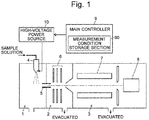
- Fig. 1 is a schematic configuration diagram of the mass spectrometer of the present embodiment.
- This mass spectrometer is an atmospheric pressure ionization mass spectrometer for analyzing a sample solution which, for example, is eluted from a column of a liquid chromatograph.
- the sample solution is sprayed from a nozzle 4 for electrospray ionization into an ionization chamber 1 maintained at substantially atmospheric pressure to ionize compounds contained in the sample solution.
- a high voltage whose polarity is changed according to the polarity of the ions to be generated, i.e. according to which of the positive and negative ion measurement modes is carried out.
- a high-voltage power source 10 which is capable of switching the polarity of the output voltage at high speeds, as will be described later, is used.
- the ions generated in the atmospheric ambience in the previously described manner are sent through a desolvation tube 5 into an intermediate vacuum chamber 2 located in the next stage, where the ions are converged by an ion lens 6 driven by a power source (not shown), and sent into a high vacuum chamber 3 maintained at a higher degree of vacuum.
- the ions are introduced into a space extending along the longitudinal axis of a quadrupole mass filter 7 placed within the high vacuum chamber 3.
- the quadrupole mass filter 7 is formed by four rod electrodes, to which a voltage composed of a radio-frequency voltage superposed on a DC voltage is applied from a voltage source (not shown).
- a main controller 9 performs analysis operations by controlling the high-voltage power source 10 and other power sources (not shown) as well as other devices according to the measurement conditions including various parameters stored in a measurement condition storage section 90.
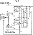
- Fig. 2 is a configuration diagram showing one example of the high-voltage power source 10, while Fig. 3 is a diagram showing a specific configuration example of the charge release assistant section 26 in Fig. 2 .
- This high-voltage power source 10 is a high-voltage power supply device disclosed in Patent Literature 3.
- the high-voltage power source 10 includes a voltage control section 20, positive voltage generation section 21, negative voltage generation section 23, and charge release assistant section 26.
- the positive voltage generation section 21 includes a boosting transformer T1, a drive circuit 22 for driving the primary winding of the transformer T1, and a rectifying circuit employing a Cockcroft-Walton circuit (composed of four capacitors C1-C4 and four diodes D1-D4) connected to the secondary winding of the transformer T1.
- the negative voltage generation section 23 has the same basic configuration as the positive voltage generation section 21 except for the diodes D5-D8 in the Cockcroft-Walton circuit which are oppositely directed to their counterparts in the positive voltage generation section 21.
- the output terminal P2 of the positive voltage generation section 21 is connected with the output terminal Q1 of the negative voltage generation section 23.
- the other output terminal Q2 of the negative voltage generation section 23 is grounded via a resistor 25.
- the charge release assistant section 26 is connected to the output terminals P1 and P2 of the positive voltage generation section 21 as well as the output terminals Q1 and Q2 of the negative voltage generation section 23.
- a parallel circuit including a series-connection circuit of resistors 60 and 61 in parallel with a switch circuit 62 is connected between the output terminals P1 and P2 of the positive voltage generation section 21, while a parallel circuit including a series-connection circuit of resistors 63 and 64 in parallel with a switch circuit 65 is connected between the output terminals Q1 and Q2 of the negative voltage generation section 23.
- the signal extracted from the connection point of the resistors 60 and 61 on the positive side is sent to the switch circuit 65 on the negative side as the on/off drive control signal.
- the signal extracted from the connection point of the resistors 63 and 64 is sent to the switch circuit 62 on the negative side as the on/off drive control signal.
- the output terminal P1 of the positive voltage generation section 21 is connected to a voltage output terminal 29 from which a high voltage having a switched polarity is provided.
- Two resistors 27 and 28 are connected in series between this voltage output terminal 29 and the ground. The voltage signal at the connection point of the resistors 27 and 28 is fed back to the voltage control section 20.
- each of the drive circuits 22 and 24 in the positive and negative voltage generators 21 and 23 includes a DC voltage source and switching element connected in series to the primary winding of the transformer T1. The voltage applied (or electric current supplied) from the DC voltage source to the primary winding is turned on and off by the switching element.
- the pulse width of a rectangular wave signal for driving the switching element to turn on and off is controlled by the voltage control section 20, whereby the amount of effective power supplied to the primary winding of the transformer T1 changes.
- the output voltages of the positive and negative voltage generation sections 21 and 23 change from zero to their respective preset levels.
- the positive voltage generation section 21 is deactivated, while the negative voltage generation section 23 is activated.
- the voltage between the output terminals P1 and P2 of the positive voltage generation section 21 begins to decrease.
- the switch circuit 65 turns off.
- the voltage (in absolute value) between the output terminals Q1 and Q2 of the negative voltage generation section 23 increases.
- the drive control signal is given to the switch circuit 62 and makes this switch circuit 62 turn on. Consequently, the electric charges remaining at the output terminal P1 of the positive voltage generation section 21 are rapidly discharged through the switch circuit 62 and quickly decreases to zero.
- the switch circuit 62 or 65 When the switch circuit 62 or 65 is in the ON state, the switch circuit 62 or 65 has an extremely low level of impedance and easily allows the passage of electric current. Conversely, when the switch circuit 62 or 65 is in the OFF state, the switch circuit 62 or 65 has an extremely high level of impedance and does not easily allow the passage of electric current.
- the switch circuits 62 and 65 are both an impedance-variable circuit whose impedance significantly changes depending on the voltage obtained by the resistive division using the resistors 60 and 61 or resistors 63 and 64.
- the charge release assistant section 26 of Fig. 2 simply illustrates its principle.
- a circuit including FETs, transistors or similar switching elements is used, as shown in Fig. 3 .
- the withstand voltage between the drain and source terminals of a FET is approximately 1 kV.
- a single FET cannot withstand an output voltage which increases to a high level of approximately ⁇ 10 kV. Accordingly, in the example shown in Fig. 3 , ten or more FETs are connected in series.
- the voltage between the output terminals P1 and P2 is divided by the series-connected resistors 601-60n and 61, with the resulting voltages respectively applied to the gate terminals of the FETs 621-62n.
- a resistor 62r is connected between the source terminal of the FET 62n located at the lowest-voltage end among the large number of series-connected FETs 621-62n and the output terminal P2. This enables the FET 62n (which is hereinafter called the "drive FET” to distinguish it from the other FETs) to control the electric current passing through the other FETs 621-62m.
- the gate terminal of the FET 62n is connected to the connection point of the resistors 64n and 63 on the negative side. In other words, a voltage obtained by the resistive division of the negative output voltage is applied to the gate terminal of the FET 62n on the positive side.
- the negative side also has a similar configuration.
- the Zener diode connected between the gate and source terminals of each FET has the function of preventing an overvoltage from being applied to the gate electrode.
- the voltage obtained by the resistive division is 10 V
- the resistance value of the resistor 65r connected to the source terminal of the drive FET 65n is 1 k ⁇
- the gate threshold (Vth) of the drive FET 65n is 4 V
- the output voltage of the negative voltage generation section 23 i.e. the voltage between output terminals Q1 and Q2
- the configuration of the charge release assistant section 26 is not limited to the one shown in Fig. 3 ; a modified configuration using transistors or similar elements is also possible, as described in Patent Literature 3. Additionally, in the circuit shown in Fig. 3 , the series-connection circuit of the FETs inclusive of the drive FET 62n or 65n may also be considered to be a current source with the maximum current limited in the previously described manner. Accordingly, each of the series-connection circuits of the FETs including the drive FET 62n or 65n can also be regarded as a variable-current source.
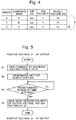
- the value of the application voltage which yields the highest level of ionization efficiency varies depending on the kind of compound. Therefore, when SIM measurements for a plurality of target compounds are performed in the previously described manner, each target compound can be detected with high sensitivity by appropriately changing the application voltage to the nozzle 4 depending on the kind of compound. Accordingly, for example, when SIM measurements for three target compounds are performed within a certain measurement time range, the optimum nozzle voltages for the target compounds are previously set as one of the measurement parameters, as shown in Fig.4 . Such a setting can be performed by analysis operators as needed.
- a table showing the relationship between the kind of compound and optimum nozzle value for a large number of compounds
- the system can be configured so that, when an analysis operator selects a target compound, the system refers to the aforementioned table (or the like) and automatically sets the optimum nozzle voltage for the selected target compound.
- a set of information as shown in Fig. 4 is stored in the measurement condition storage section 90 as one of the measurement conditions.
- the main controller 9 When an analysis is initiated, the main controller 9 performs the analysis by controlling the high-voltage power source 10 and other power sources (not shown) as well as other devices according to the measurement conditions stored in the measurement condition storage section 90. Within the aforementioned measurement time range, the main controller 9 refers to the information shown in Fig. 4 (and other information sources) and controls relevant sections so that SIM measurements aimed at specific ions whose mass-to-charge ratios respectively correspond to the three compounds A, B and C are repeated with a predetermined cycle. In this process, the voltage applied to the nozzle 4 needs to be cyclically changed as follows: +5 kV ⁇ +2 kV ⁇ +3 kV ⁇ +5 kV ⁇ ....
- the voltage control section 20 operates the positive and negative voltage generation sections 21 and 23 so as to initially reverse the polarity of the output voltage (Step S2).
- the target voltage in this step may have any value whose polarity is negative, such as -V 1 , -V 2 or other appropriate values.
- the voltage control section 20 maintains this state until a predetermined period of time passes from the polarity-switching control ("No" in Step S3).
- the voltage control section 20 changes the target voltage to V 2 and operates the positive and negative voltage generation sections 21 and 23 so as to once more reverse the polarity of the output voltage (Step S4).
- the predetermined period of time used in this process can be experimentally determined beforehand. As already explained, if the output voltage is changed so that the voltage decreases without changing its polarity, a considerable amount of time is required for the decrease in the voltage since the electric charges accumulated at the output terminals are merely discharged through the loading resistor (e.g. resistors 60 and 61 in Fig. 5 ).
- Fig. 6A is an actually measured waveform of the voltage change in the process of changing the voltage from +5 kV to +2 kV in a conventional device. This voltage-changing operation required approximately 15 msec.
- Fig. 6B is an actually measured waveform of the voltage change in the process of changing the voltage from +5 kV to +2 kV in the device of the present embodiment. Due to the rapid decrease in the output voltage induced by the polarity-reversing operation, the total length of time for the voltage-changing operation was shortened to approximately 2 msec.
- the predetermined period of time used in Step S3 in the present example is tuned to an almost optimum value so that the voltage decreasing from +5 kV after the reversal of the polarity will revert to the previous polarity before the voltage becomes negative.
- a strict tuning of the predetermined period of time is not always necessary. For example, a slight increase in the predetermined period of time which causes the voltage decreasing from the +5 kV to be temporarily negative is allowable if the total amount of time for the voltage-changing operation is sufficiently shorter than in the case where the polarity-reversing operation is not performed.
- the previous example is concerned with the case of decreasing a positive voltage without changing its polarity.
- the idea of increasing the speed of the voltage-changing operation by the temporary polarity-reversing control is also evidently applicable in the case of decreasing the absolute value of a negative voltage without changing its polarity, e.g. when the voltage is changed from -5 kV to -2 kV.
- the previous embodiment is concerned with the present invention applied in a single-type quadrupole mass spectrometer.
- the present invention is also applicable in a tandem quadrupole mass spectrometer including two quadrupole mass filters placed before and after a collision cell.
- tandem quadruple mass spectrometers are commonly used for simultaneous multi-component analysis due to their high level of ion-selection capability. If there are a large number of compounds to be simultaneously analyzed, only a short period of MRM measurement time is available for one transition, and the operation of changing the output voltage from the high-voltage power source also needs to be performed at high speeds. Accordingly, the present invention is extremely useful in the case of performing MRM measurements in a tandem quadrupole mass spectrometer.
- the voltage generated by the high-voltage power source is applied to the nozzle of the ESI ion source.
- the present invention is also applicable in a mass spectrometer using a different type of ion source which requires an application of a high voltage.
- the present invention may also be applied in a section other than the ion source, such as an ion detector, which similarly needs an application of a high voltage generated by a high-voltage power source.
- the mass spectrometer of the previous embodiment can selectively perform one of the positive and negative ion measurements by switching the polarity of the high voltage applied to the nozzle 4 of the ESI ion source.
- the present invention is also applicable in a mass spectrometer capable of only one of the positive and negative ion measurements.
- a high-voltage power source which is actually capable of the high-speed positive/negative switching of the polarity of the output voltage, and utilize its polarity-switching function to increase the speed of the operation of changing the voltage with the same polarity.
Landscapes
- Chemical & Material Sciences (AREA)
- Analytical Chemistry (AREA)
- Engineering & Computer Science (AREA)
- Physics & Mathematics (AREA)
- Plasma & Fusion (AREA)
- Power Engineering (AREA)
- Other Investigation Or Analysis Of Materials By Electrical Means (AREA)
- Electron Tubes For Measurement (AREA)
- Rectifiers (AREA)
Applications Claiming Priority (1)
| Application Number | Priority Date | Filing Date | Title |
|---|---|---|---|
| PCT/JP2014/077827 WO2016063329A1 (fr) | 2014-10-20 | 2014-10-20 | Spectroscope de masse |
Publications (2)
| Publication Number | Publication Date |
|---|---|
| EP3211781A1 true EP3211781A1 (fr) | 2017-08-30 |
| EP3211781A4 EP3211781A4 (fr) | 2017-11-22 |
Family
ID=55760404
Family Applications (1)
| Application Number | Title | Priority Date | Filing Date |
|---|---|---|---|
| EP14904426.5A Withdrawn EP3211781A4 (fr) | 2014-10-20 | 2014-10-20 | Spectroscope de masse |
Country Status (5)
| Country | Link |
|---|---|
| US (1) | US10229822B2 (fr) |
| EP (1) | EP3211781A4 (fr) |
| JP (1) | JP6237924B2 (fr) |
| CN (1) | CN107078653B (fr) |
| WO (1) | WO2016063329A1 (fr) |
Cited By (10)
| Publication number | Priority date | Publication date | Assignee | Title |
|---|---|---|---|---|
| US11355331B2 (en) | 2018-05-31 | 2022-06-07 | Micromass Uk Limited | Mass spectrometer |
| US11367607B2 (en) | 2018-05-31 | 2022-06-21 | Micromass Uk Limited | Mass spectrometer |
| US11373849B2 (en) | 2018-05-31 | 2022-06-28 | Micromass Uk Limited | Mass spectrometer having fragmentation region |
| US11437226B2 (en) | 2018-05-31 | 2022-09-06 | Micromass Uk Limited | Bench-top time of flight mass spectrometer |
| US11476103B2 (en) | 2018-05-31 | 2022-10-18 | Micromass Uk Limited | Bench-top time of flight mass spectrometer |
| US11538676B2 (en) | 2018-05-31 | 2022-12-27 | Micromass Uk Limited | Mass spectrometer |
| US11621154B2 (en) | 2018-05-31 | 2023-04-04 | Micromass Uk Limited | Bench-top time of flight mass spectrometer |
| US11879470B2 (en) | 2018-05-31 | 2024-01-23 | Micromass Uk Limited | Bench-top time of flight mass spectrometer |
| US12009193B2 (en) | 2018-05-31 | 2024-06-11 | Micromass Uk Limited | Bench-top Time of Flight mass spectrometer |
| US12027359B2 (en) | 2018-05-31 | 2024-07-02 | Micromass Uk Limited | Bench-top Time of Flight mass spectrometer |
Families Citing this family (7)
| Publication number | Priority date | Publication date | Assignee | Title |
|---|---|---|---|---|
| US10473634B2 (en) * | 2014-06-12 | 2019-11-12 | Shimadzu Corporation | Data processing device for mass spectrometry and program for said device |
| CN109643637B (zh) * | 2016-08-22 | 2021-06-18 | 株式会社岛津制作所 | 飞行时间质谱分析装置 |
| EP4056995A4 (fr) * | 2019-11-06 | 2023-12-20 | Shimadzu Corporation | Spectromètre de masse à temps de vol et procédé d'analyse |
| US11145502B2 (en) * | 2019-12-19 | 2021-10-12 | Thermo Finnigan Llc | Emission current measurement for superior instrument-to-instrument repeatability |
| JP7323058B2 (ja) * | 2020-04-17 | 2023-08-08 | 株式会社島津製作所 | イオン分析装置 |
| CN116338762A (zh) * | 2023-03-03 | 2023-06-27 | 北京华粤瑞科科技有限公司 | 一种辐射剂量仪 |
| CN117080046B (zh) * | 2023-10-17 | 2024-01-19 | 湖南豪思生物科技有限公司 | 高压极性高速切换装置及其质谱仪 |
Family Cites Families (13)
| Publication number | Priority date | Publication date | Assignee | Title |
|---|---|---|---|---|
| US6002600A (en) | 1994-11-08 | 1999-12-14 | Spellman High Voltage Co. | Reversible polarity high voltage power supply |
| JP3294981B2 (ja) * | 1995-11-30 | 2002-06-24 | 日本電子株式会社 | 分析装置及び高圧電源装置 |
| CN1247644A (zh) * | 1997-12-25 | 2000-03-15 | 三菱电机株式会社 | 脉冲电源装置 |
| JP2004040915A (ja) * | 2002-07-03 | 2004-02-05 | Shimadzu Corp | 高電圧発生用電源回路 |
| US7855355B2 (en) * | 2005-09-08 | 2010-12-21 | Shimadzu Corporation | High-voltage power unit and mass spectrometer using the power unit |
| JP4902230B2 (ja) * | 2006-03-09 | 2012-03-21 | 株式会社日立ハイテクノロジーズ | 質量分析装置 |
| WO2008126383A1 (fr) * | 2007-04-09 | 2008-10-23 | Shimadzu Corporation | Spectrographe de masse à piège ionique |
| GB0809950D0 (en) * | 2008-05-30 | 2008-07-09 | Thermo Fisher Scient Bremen | Mass spectrometer |
| US9378936B2 (en) * | 2012-01-24 | 2016-06-28 | Dh Technologies Development Pte. Ltd. | Fast switching, dual polarity, dual output high voltage power supply |
| US9431226B2 (en) * | 2012-11-05 | 2016-08-30 | Shimadzu Corporation | High-voltage power unit and mass spectrometer using the power unit |
| EP2988317B1 (fr) * | 2013-05-08 | 2023-03-22 | Shimadzu Corporation | Spectrometre de masse |
| WO2015011783A1 (fr) * | 2013-07-23 | 2015-01-29 | 株式会社島津製作所 | Dispositif d'alimentation électrique à haute tension et dispositif de spectrométrie de masse l'utilisant |
| US9929001B2 (en) * | 2014-09-17 | 2018-03-27 | Shimadzu Corporation | Mass spectrometer |
-
2014
- 2014-10-20 US US15/520,112 patent/US10229822B2/en active Active
- 2014-10-20 WO PCT/JP2014/077827 patent/WO2016063329A1/fr not_active Ceased
- 2014-10-20 EP EP14904426.5A patent/EP3211781A4/fr not_active Withdrawn
- 2014-10-20 JP JP2016554960A patent/JP6237924B2/ja active Active
- 2014-10-20 CN CN201480082780.7A patent/CN107078653B/zh active Active
Cited By (13)
| Publication number | Priority date | Publication date | Assignee | Title |
|---|---|---|---|---|
| US11355331B2 (en) | 2018-05-31 | 2022-06-07 | Micromass Uk Limited | Mass spectrometer |
| US11367607B2 (en) | 2018-05-31 | 2022-06-21 | Micromass Uk Limited | Mass spectrometer |
| GB2602188A (en) * | 2018-05-31 | 2022-06-22 | Micromass Ltd | Mass spectrometer |
| US11373849B2 (en) | 2018-05-31 | 2022-06-28 | Micromass Uk Limited | Mass spectrometer having fragmentation region |
| US11437226B2 (en) | 2018-05-31 | 2022-09-06 | Micromass Uk Limited | Bench-top time of flight mass spectrometer |
| US11476103B2 (en) | 2018-05-31 | 2022-10-18 | Micromass Uk Limited | Bench-top time of flight mass spectrometer |
| US11538676B2 (en) | 2018-05-31 | 2022-12-27 | Micromass Uk Limited | Mass spectrometer |
| GB2602188B (en) * | 2018-05-31 | 2023-01-11 | Micromass Ltd | Mass spectrometer |
| US11621154B2 (en) | 2018-05-31 | 2023-04-04 | Micromass Uk Limited | Bench-top time of flight mass spectrometer |
| US11848187B2 (en) | 2018-05-31 | 2023-12-19 | Micromass Uk Limited | Mass spectrometer |
| US11879470B2 (en) | 2018-05-31 | 2024-01-23 | Micromass Uk Limited | Bench-top time of flight mass spectrometer |
| US12009193B2 (en) | 2018-05-31 | 2024-06-11 | Micromass Uk Limited | Bench-top Time of Flight mass spectrometer |
| US12027359B2 (en) | 2018-05-31 | 2024-07-02 | Micromass Uk Limited | Bench-top Time of Flight mass spectrometer |
Also Published As
| Publication number | Publication date |
|---|---|
| CN107078653B (zh) | 2019-07-23 |
| JP6237924B2 (ja) | 2017-11-29 |
| EP3211781A4 (fr) | 2017-11-22 |
| US10229822B2 (en) | 2019-03-12 |
| JPWO2016063329A1 (ja) | 2017-04-27 |
| CN107078653A (zh) | 2017-08-18 |
| US20170323773A1 (en) | 2017-11-09 |
| WO2016063329A1 (fr) | 2016-04-28 |
Similar Documents
| Publication | Publication Date | Title |
|---|---|---|
| US10229822B2 (en) | Mass spectrometer with high-voltage power source | |
| US9431226B2 (en) | High-voltage power unit and mass spectrometer using the power unit | |
| EP3196640B1 (fr) | Spectromètre de masse | |
| EP3404695B1 (fr) | Spectromètre de masse à temps de vol | |
| US7855355B2 (en) | High-voltage power unit and mass spectrometer using the power unit | |
| CN111224540A (zh) | 开关电容变换器及其驱动电路 | |
| US10984997B2 (en) | Mass spectrometer with main voltage generating unit and auxiliary power supply | |
| US9583324B2 (en) | High-voltage power unit and mass spectrometer using the power unit | |
| JP6167934B2 (ja) | 質量分析装置 | |
| US7643267B2 (en) | Optical emission spectrometry device | |
| US11101127B2 (en) | Time-of-flight mass spectrometer | |
| US11373851B2 (en) | High-voltage power supply device | |
| WO2019229915A1 (fr) | Dispositif de spectrométrie de masse à temps de vol | |
| CN1854717B (zh) | 发光分析装置 | |
| US8502973B2 (en) | Optical emission analyzer | |
| WO2016062738A1 (fr) | Dispositif de commande de leds | |
| HK1154117A (en) | End cap voltage control of ion traps |
Legal Events
| Date | Code | Title | Description |
|---|---|---|---|
| PUAI | Public reference made under article 153(3) epc to a published international application that has entered the european phase |
Free format text: ORIGINAL CODE: 0009012 |
|
| 17P | Request for examination filed |
Effective date: 20170505 |
|
| AK | Designated contracting states |
Kind code of ref document: A1 Designated state(s): AL AT BE BG CH CY CZ DE DK EE ES FI FR GB GR HR HU IE IS IT LI LT LU LV MC MK MT NL NO PL PT RO RS SE SI SK SM TR |
|
| AX | Request for extension of the european patent |
Extension state: BA ME |
|
| A4 | Supplementary search report drawn up and despatched |
Effective date: 20171020 |
|
| RIC1 | Information provided on ipc code assigned before grant |
Ipc: H02M 7/10 20060101AFI20171016BHEP |
|
| DAX | Request for extension of the european patent (deleted) | ||
| 17Q | First examination report despatched |
Effective date: 20180524 |
|
| GRAP | Despatch of communication of intention to grant a patent |
Free format text: ORIGINAL CODE: EPIDOSNIGR1 |
|
| INTG | Intention to grant announced |
Effective date: 20191120 |
|
| STAA | Information on the status of an ep patent application or granted ep patent |
Free format text: STATUS: THE APPLICATION IS DEEMED TO BE WITHDRAWN |
|
| 18D | Application deemed to be withdrawn |
Effective date: 20200603 |