EP3211977B1 - Leiterplatte mit antennenstruktur und verfahren zu dessen herstellung - Google Patents
Leiterplatte mit antennenstruktur und verfahren zu dessen herstellung Download PDFInfo
- Publication number
- EP3211977B1 EP3211977B1 EP17158161.4A EP17158161A EP3211977B1 EP 3211977 B1 EP3211977 B1 EP 3211977B1 EP 17158161 A EP17158161 A EP 17158161A EP 3211977 B1 EP3211977 B1 EP 3211977B1
- Authority
- EP
- European Patent Office
- Prior art keywords
- layer
- antenna
- printed circuit
- circuit board
- cavity
- Prior art date
- Legal status (The legal status is an assumption and is not a legal conclusion. Google has not performed a legal analysis and makes no representation as to the accuracy of the status listed.)
- Active
Links
Images




Classifications
-
- H—ELECTRICITY
- H05—ELECTRIC TECHNIQUES NOT OTHERWISE PROVIDED FOR
- H05K—PRINTED CIRCUITS; CASINGS OR CONSTRUCTIONAL DETAILS OF ELECTRIC APPARATUS; MANUFACTURE OF ASSEMBLAGES OF ELECTRICAL COMPONENTS
- H05K3/00—Apparatus or processes for manufacturing printed circuits
- H05K3/46—Manufacturing multilayer circuits
- H05K3/4688—Composite multilayer circuits, i.e. comprising insulating layers having different properties
-
- H—ELECTRICITY
- H01—ELECTRIC ELEMENTS
- H01Q—ANTENNAS, i.e. RADIO AERIALS
- H01Q1/00—Details of, or arrangements associated with, antennas
- H01Q1/36—Structural form of radiating elements, e.g. cone, spiral, umbrella; Particular materials used therewith
- H01Q1/38—Structural form of radiating elements, e.g. cone, spiral, umbrella; Particular materials used therewith formed by a conductive layer on an insulating support
-
- H—ELECTRICITY
- H01—ELECTRIC ELEMENTS
- H01Q—ANTENNAS, i.e. RADIO AERIALS
- H01Q1/00—Details of, or arrangements associated with, antennas
- H01Q1/44—Details of, or arrangements associated with, antennas using equipment having another main function to serve additionally as an antenna, e.g. means for giving an antenna an aesthetic aspect
-
- H—ELECTRICITY
- H01—ELECTRIC ELEMENTS
- H01Q—ANTENNAS, i.e. RADIO AERIALS
- H01Q1/00—Details of, or arrangements associated with, antennas
- H01Q1/48—Earthing means; Earth screens; Counterpoises
-
- H—ELECTRICITY
- H05—ELECTRIC TECHNIQUES NOT OTHERWISE PROVIDED FOR
- H05K—PRINTED CIRCUITS; CASINGS OR CONSTRUCTIONAL DETAILS OF ELECTRIC APPARATUS; MANUFACTURE OF ASSEMBLAGES OF ELECTRICAL COMPONENTS
- H05K1/00—Printed circuits
- H05K1/02—Details
- H05K1/0213—Electrical arrangements not otherwise provided for
- H05K1/0216—Reduction of cross-talk, noise or electromagnetic interference
- H05K1/0218—Reduction of cross-talk, noise or electromagnetic interference by printed shielding conductors, ground planes or power plane
- H05K1/0219—Printed shielding conductors for shielding around or between signal conductors, e.g. coplanar or coaxial printed shielding conductors
-
- H—ELECTRICITY
- H05—ELECTRIC TECHNIQUES NOT OTHERWISE PROVIDED FOR
- H05K—PRINTED CIRCUITS; CASINGS OR CONSTRUCTIONAL DETAILS OF ELECTRIC APPARATUS; MANUFACTURE OF ASSEMBLAGES OF ELECTRICAL COMPONENTS
- H05K1/00—Printed circuits
- H05K1/02—Details
- H05K1/0213—Electrical arrangements not otherwise provided for
- H05K1/0216—Reduction of cross-talk, noise or electromagnetic interference
- H05K1/0218—Reduction of cross-talk, noise or electromagnetic interference by printed shielding conductors, ground planes or power plane
- H05K1/0219—Printed shielding conductors for shielding around or between signal conductors, e.g. coplanar or coaxial printed shielding conductors
- H05K1/0222—Printed shielding conductors for shielding around or between signal conductors, e.g. coplanar or coaxial printed shielding conductors for shielding around a single via or around a group of vias, e.g. coaxial vias or vias surrounded by a grounded via fence
-
- H—ELECTRICITY
- H05—ELECTRIC TECHNIQUES NOT OTHERWISE PROVIDED FOR
- H05K—PRINTED CIRCUITS; CASINGS OR CONSTRUCTIONAL DETAILS OF ELECTRIC APPARATUS; MANUFACTURE OF ASSEMBLAGES OF ELECTRICAL COMPONENTS
- H05K1/00—Printed circuits
- H05K1/02—Details
- H05K1/0296—Conductive pattern lay-out details not covered by sub groups H05K1/02 - H05K1/0295
- H05K1/0298—Multilayer circuits
-
- H—ELECTRICITY
- H05—ELECTRIC TECHNIQUES NOT OTHERWISE PROVIDED FOR
- H05K—PRINTED CIRCUITS; CASINGS OR CONSTRUCTIONAL DETAILS OF ELECTRIC APPARATUS; MANUFACTURE OF ASSEMBLAGES OF ELECTRICAL COMPONENTS
- H05K1/00—Printed circuits
- H05K1/02—Details
- H05K1/11—Printed elements for providing electric connections to or between printed circuits
- H05K1/115—Via connections; Lands around holes or via connections
-
- H—ELECTRICITY
- H05—ELECTRIC TECHNIQUES NOT OTHERWISE PROVIDED FOR
- H05K—PRINTED CIRCUITS; CASINGS OR CONSTRUCTIONAL DETAILS OF ELECTRIC APPARATUS; MANUFACTURE OF ASSEMBLAGES OF ELECTRICAL COMPONENTS
- H05K1/00—Printed circuits
- H05K1/16—Printed circuits incorporating printed electric components, e.g. printed resistors, capacitors or inductors
-
- H—ELECTRICITY
- H05—ELECTRIC TECHNIQUES NOT OTHERWISE PROVIDED FOR
- H05K—PRINTED CIRCUITS; CASINGS OR CONSTRUCTIONAL DETAILS OF ELECTRIC APPARATUS; MANUFACTURE OF ASSEMBLAGES OF ELECTRICAL COMPONENTS
- H05K1/00—Printed circuits
- H05K1/18—Printed circuits structurally associated with non-printed electric components
- H05K1/182—Printed circuits structurally associated with non-printed electric components associated with components mounted in printed circuit boards [PCB], e.g. insert-mounted components [IMC]
- H05K1/185—Printed circuits structurally associated with non-printed electric components associated with components mounted in printed circuit boards [PCB], e.g. insert-mounted components [IMC] associated with components encapsulated in the insulating substrate of the PCBs; associated with components incorporated in internal layers of multilayer circuit boards
-
- H—ELECTRICITY
- H05—ELECTRIC TECHNIQUES NOT OTHERWISE PROVIDED FOR
- H05K—PRINTED CIRCUITS; CASINGS OR CONSTRUCTIONAL DETAILS OF ELECTRIC APPARATUS; MANUFACTURE OF ASSEMBLAGES OF ELECTRICAL COMPONENTS
- H05K3/00—Apparatus or processes for manufacturing printed circuits
- H05K3/22—Secondary treatment of printed circuits
- H05K3/28—Applying non-metallic protective coatings
- H05K3/282—Applying non-metallic protective coatings for inhibiting the corrosion of the circuit, e.g. for preserving the solderability
-
- H—ELECTRICITY
- H05—ELECTRIC TECHNIQUES NOT OTHERWISE PROVIDED FOR
- H05K—PRINTED CIRCUITS; CASINGS OR CONSTRUCTIONAL DETAILS OF ELECTRIC APPARATUS; MANUFACTURE OF ASSEMBLAGES OF ELECTRICAL COMPONENTS
- H05K3/00—Apparatus or processes for manufacturing printed circuits
- H05K3/40—Forming printed elements for providing electric connections to or between printed circuits
- H05K3/4038—Through-connections; Vertical interconnect access [VIA] connections
-
- H—ELECTRICITY
- H05—ELECTRIC TECHNIQUES NOT OTHERWISE PROVIDED FOR
- H05K—PRINTED CIRCUITS; CASINGS OR CONSTRUCTIONAL DETAILS OF ELECTRIC APPARATUS; MANUFACTURE OF ASSEMBLAGES OF ELECTRICAL COMPONENTS
- H05K3/00—Apparatus or processes for manufacturing printed circuits
- H05K3/46—Manufacturing multilayer circuits
- H05K3/4644—Manufacturing multilayer circuits by building the multilayer layer by layer, i.e. build-up multilayer circuits
-
- H—ELECTRICITY
- H05—ELECTRIC TECHNIQUES NOT OTHERWISE PROVIDED FOR
- H05K—PRINTED CIRCUITS; CASINGS OR CONSTRUCTIONAL DETAILS OF ELECTRIC APPARATUS; MANUFACTURE OF ASSEMBLAGES OF ELECTRICAL COMPONENTS
- H05K3/00—Apparatus or processes for manufacturing printed circuits
- H05K3/46—Manufacturing multilayer circuits
- H05K3/4697—Manufacturing multilayer circuits having cavities, e.g. for mounting components
-
- H—ELECTRICITY
- H01—ELECTRIC ELEMENTS
- H01Q—ANTENNAS, i.e. RADIO AERIALS
- H01Q19/00—Combinations of primary active antenna elements and units with secondary devices, e.g. with quasi-optical devices, for giving the antenna a desired directional characteristic
- H01Q19/10—Combinations of primary active antenna elements and units with secondary devices, e.g. with quasi-optical devices, for giving the antenna a desired directional characteristic using reflecting surfaces
-
- H—ELECTRICITY
- H05—ELECTRIC TECHNIQUES NOT OTHERWISE PROVIDED FOR
- H05K—PRINTED CIRCUITS; CASINGS OR CONSTRUCTIONAL DETAILS OF ELECTRIC APPARATUS; MANUFACTURE OF ASSEMBLAGES OF ELECTRICAL COMPONENTS
- H05K2201/00—Indexing scheme relating to printed circuits covered by H05K1/00
- H05K2201/07—Electric details
- H05K2201/0707—Shielding
- H05K2201/0723—Shielding provided by an inner layer of PCB
-
- H—ELECTRICITY
- H05—ELECTRIC TECHNIQUES NOT OTHERWISE PROVIDED FOR
- H05K—PRINTED CIRCUITS; CASINGS OR CONSTRUCTIONAL DETAILS OF ELECTRIC APPARATUS; MANUFACTURE OF ASSEMBLAGES OF ELECTRICAL COMPONENTS
- H05K2201/00—Indexing scheme relating to printed circuits covered by H05K1/00
- H05K2201/09—Shape and layout
- H05K2201/09209—Shape and layout details of conductors
- H05K2201/0929—Conductive planes
-
- H—ELECTRICITY
- H05—ELECTRIC TECHNIQUES NOT OTHERWISE PROVIDED FOR
- H05K—PRINTED CIRCUITS; CASINGS OR CONSTRUCTIONAL DETAILS OF ELECTRIC APPARATUS; MANUFACTURE OF ASSEMBLAGES OF ELECTRICAL COMPONENTS
- H05K2201/00—Indexing scheme relating to printed circuits covered by H05K1/00
- H05K2201/10—Details of components or other objects attached to or integrated in a printed circuit board
- H05K2201/10007—Types of components
- H05K2201/10098—Components for radio transmission, e.g. radio frequency identification [RFID] tag, printed or non-printed antennas
-
- H—ELECTRICITY
- H05—ELECTRIC TECHNIQUES NOT OTHERWISE PROVIDED FOR
- H05K—PRINTED CIRCUITS; CASINGS OR CONSTRUCTIONAL DETAILS OF ELECTRIC APPARATUS; MANUFACTURE OF ASSEMBLAGES OF ELECTRICAL COMPONENTS
- H05K2203/00—Indexing scheme relating to apparatus or processes for manufacturing printed circuits covered by H05K3/00
- H05K2203/06—Lamination
Definitions
- the present invention relates to methods for producing an intermediate printed circuit board product with an antenna structure for high-frequency applications.
- the present invention also relates to an intermediate printed circuit board product as well as a printed circuit board with an antenna structure.
- PCB printed circuit boards
- FR-4 (or FR4) is a grade designation assigned to glass-reinforced epoxy laminate sheets, tubes, rods and printed circuit boards (PCB).
- PCB printed circuit boards
- RF laminates RF short for Radio Frequency
- PTFE PolyTetraFluoroEthylene, Teflon®
- hydrocarbon ceramic laminates are designed to offer superior high frequency performance but are very expensive. Also the process efforts and process costs in PCB manufacturing are very high when these RF laminates are applied.
- microstrip antennas In telecommunication, there are several types of microstrip antennas that are also known as printed antennas. The most common of which is the microstrip patch antenna or patch antenna, respectively.
- a patch antenna that is also known as a rectangular microstrip antenna is a type of radio antenna with a low profile, which can be mounted on a flat surface. Commonly it consists of a flat rectangular sheet or patch of metal or a conductive material, mounted over a larger sheet of metal called a ground plane.
- the assembly is usually contained inside a housing like a plastic radome, which protects the antenna structure from damage. Patch antennas are simple to fabricate and easy to modify and customize.
- a patch antenna is usually constructed on a dielectric substrate, using the same materials and lithography processes used to make printed circuit boards. For example the documents EP 1 501 155 A1 , JP 2002-151911 A , JP 1996-111609 A and WO 2008/102950 A1 show different embodiments of these antennas.
- Document US 5,444,453 A discloses a microstrip antenna structure having an air gap between a radiator patch that is affixed on an inside of a thin substrate layer and a ground plane.
- the radiator patch made of a conductive material is attached the thin substrate layer made of a dielectric material forming a radiator layer.
- To maintain a substantially uniform air gap between the radiator patch and the ground plane several support posts of a predetermined thickness as well as of the same, dimple shape have to be arranged between the radiator layer and the ground layer.
- a chip package in another document US 2012/0212384 A1 a chip package is shown that includes a plurality of layers including conductive planes connected by vias.
- the layers include a first portion with an antenna formed therein and a parallel-plate mode suppression mechanism to suppress parallel-plate mode excitation of the antenna.
- the parallel-plate mode suppression mechanism includes a reflector between an antenna cavity and a ground plane that separates the first portion from a second portion of layers.
- a patch antenna On the inner side of the antenna cavity a patch antenna is mounted.
- On the ground plane an integrated circuit device is surface mounted.
- the prior art comprises also document WO-A1-2007130027 , which discloses a wireless module including a top layer, a bottom layer, and an adhesive tape to connect the top layer to the bottom layer.
- the top layer is a two-sided PCB and comprises an antenna array.
- the bottom layer comprises a double clad core with a cavity connected to a bottom two-sided PCB by an adhesive tape.
- an object of the present invention is to provide an improved method to construct an antenna structure for high speed or respective high frequency applications that can be realized at a highest-possible share with laminate materials like FR-4-based laminates which are used in standard PCB production and which have the benefit of high uptime as well as low raw material costs.
- Another, more specific object of the present invention is to provide an improved construction method for the aforementioned antenna structures wherein - compared with a default PCB production process - no additional process steps or auxiliary tools for process equipment are required.
- a further object of the present invention is to provide a method for producing an intermediate printed circuit board product or a printed circuit board with an antenna structure, wherein the antenna or microstrip antenna structure and the digital application are arranged within the same printed circuit board, preferably within the same layers of the PCB, to avoid additional physical connectors like cables between an antenna area and a digital application area.
- Another aim of the present invention is to preferably avoid usage of expensive RF laminates like PTFE-based materials or hydrocarbon ceramic laminates to achieve superior high frequency performance for high-frequency applications when producing an intermediate printed circuit board product or a printed circuit board, respectively.
- a further, even more specific aim of the present invention is to decouple required Radio Frequency (RF) properties of the antenna structure from the material properties of the laminates used to build up the antenna structure.
- RF Radio Frequency
- an antenna cavity of an antenna structure can be integrated within an intermediate printed circuit board product made of standardized laminate stack materials.
- the at least one antenna cavity within the PCB is filled with air that shows best conditions for low insertion and transmission losses due to its low dielectric constant DC of 1,0.
- the stacked-up layers made of standard laminate material like FR-4 laminate sheets and/or conducting layers exemplarily made of copper that cover the antenna cavity on its both opposite sides contribute only with a small share to the total relative permittivity of the printed circuit board.
- the respective relative permittivities of the dielectric laminates applied have comparably minor relevance or no relevance, respectively, in order to achieve superior high frequency performance of the antenna structure for high-frequency applications.
- the properties of the dielectric laminate material can be selected and optimized according to individual target parameters of the respective application, for example to optimize heat management targets of the dielectric material or for economic targets to use cheap and readily available materials.
- selection of dielectric materials is no longer a compromise between Radio Frequency (RF) and other applications but can be optimized for any other purpose which is a major advantage of the invention that enhances flexibility of the respective production method decisively.
- Manufacturing of the antenna cavity within the first semi-finished product can be made for example via a laser cutting-, punching-, etching- and/or deep routing process.
- a release layer that is attached on the ground layer and that defines the shape of the antenna subarea, can be of advantage.
- a cavity projection area that corresponds to the release layer shape can be obtained, wherein the ground-plane area of the cavity is covered by the release layer.
- After manufacturing the antenna cavity it can be opened like a plug by peeling off the release layer. This manufacturing feature is also known as 2.5D technology developed by the applicant.
- the depth of the antenna cavity is flexible and can be adapted according to individual requirements.
- DF dissipation factor
- the depth of the antenna cavity can be adjusted in relation to the inductance of a patch antenna.
- the antenna design area can be adjusted in relation to the depth of the cavity which is another advantage of the invention.
- the antenna cavity height can be adjusted equal to the sum of at least one conducting layer height and at least one dielectric insulating layer height. If applicable a cavity projection area corresponds to the release layer shape and is positioned on the antenna subarea covered by the release layer and wherein a ground-plane area of the cavity is made up of the release layer.
- a layer arrangement comprising at least one further dielectric insulating layer and at least one further conducting layer can be attached to or stacked up on said conducting layer.
- the layer arrangement can comprise even or uneven numbers of layers.
- the layer arrangement can comprise for example in one embodiment further dielectric insulating layers and further conducting layers that are alternatingly and pairwise positioned within the layer arrangement.
- said layer arrangement can also comprise two or more further dielectric insulating layers that are stacked up directly next to one another forming a multi-layered dielectric insulating layer arrangement, before a further conducting layer is arranged.
- asymmetrical layer build-ups are covered by said layer arrangement. According to the number of layers comprised within the layer arrangement and their respective layer heights, the cavity height of the antenna cavity can be adjusted.
- a metallic coating of the side walls works as metalized shielding which increases antenna signal reflection and reduces signal losses.
- Metallic coating can also shield any digital processing structure that is arranged on board and prevent or at least reduce the risk of electric and electrostatic discharges within the PCB.
- copper or other metals that are regularly used for immersion coating endsurface processes like nickel, gold, tinn and/or silver can be used as metal coating materials.
- the alternative method for producing an intermediate printed circuit board according to claim 2 provides the advantage that the at least one antenna cavity can be pre-formed via recesses within the one or more dielectric insulating layer as well as within the one or more conducting layer.
- materials are used as insulating layer and/or conducting layer.
- Low-flow prepregs are prepregs which are modified to reduce or limit their resin flow during lamination and hardening.
- cut-out areas or recesses, respectively can be realised within these materials that cannot tolerate resin flowing in.
- manufacturing of the recesses within the layers can be made for example via a laser cutting-, punching-, etching- and/or deep routing process.
- conducting layers and/or insulating layers without pre-built recesses that firstly cover the respective recesses of a dielectric insulating layer underneath.
- the recesses within the conducting layers and/or insulating layers that have to be in registry with the respective recesses of the dielectric insulating layers beneath can be manufactured also on the spot via a material-removal process like milling.
- the compound signal layer can comprise a dielectric no-flow prepreg layer and a conducting metal layer that is directly attached to the dielectric no-flow prepreg layer wherein the dielectric no-flow prepreg layer is attached to the conducting layer of the first semi-finished product.
- the compound signal layer comprising two layers is provided in advance before attaching it on the exterior side made up of the conducting layer of the first semi-finished product to cover the antenna cavity.
- the dielectric no-flow prepreg layer covering the antenna cavity provides a flat surface to carry the antenna structure.
- the compound signal layer can be prepared before laminating it to obtain an intermediate printed circuit board product.
- the conducting metal layer which is attached to the dielectric no-flow prepreg layer, is recessed in cavity projection areas where one or several antenna cavities are located beneath.
- the dielectric no-flow prepreg layer keeps its flat surface also during lamination in that region where it serves as antenna cavity cover.
- the ground layer can be made of a laminated compound layer comprising at least two conducting metal layers laminated with an insulating layer in between the at least two conducting metal layers. Usage of a pre-laminated compound layer as ground layer improves production handling and reduces production costs.
- a layer arrangement comprising at least one further insulating layer and at least one further conducting metal layer can be stacked up and laminated with the preceding layers to form the laminated compound layer.
- These further layers can be laminated in one single lamination step or alternatively in two or more separate lamination steps to receive a laminated compound layer that serves as ground layer according to the invention.
- a further insulating layer and a further conducting metal layer can be stacked alternately and can be laminated with the preceding layers to form the laminated compound layer or ground layer, respectively.
- asymmetrical layer build-up is possible wherein for example two or more insulating layers can be stacked up directly next to one another.
- the antenna cavity can have a vent through-hole arranged between the ground-plane area of the cavity and an exterior side of the intermediate printed circuit board product.
- the vent through-hole ensures that a pressure compensation can take place between the inside pressure within the antenna cavity and the surrounding pressure outside of the PCB.
- the antenna cavity can be surrounded with shielding vias that are arranged within the laminated ground layer and/or at least one dielectric insulating layer and/or conducting layer and/or compound signal layer in a distance in regard to the antenna cavity.
- Shielding vias act as electric screen to shield the antenna structure and the antenna cavity, respectively, from electric and electrostatic discharges within the PCB.
- the shielding vias enhance the mechanical strength of the intermediate printed circuit board product or the printed circuit board, respectively.
- the shielding vias are positioned in extension to the corners of the at least one antenna cavity.
- the antenna structure can comprise an antenna design area that is arranged on an exterior side of the compound signal layer.
- the antenna design area is attached on the dielectric no-flow prepreg layer as this layer provides a flat surface and covers the antenna cavity located beneath.
- the antenna design area is attached on the upper exterior side of the dielectric no-flow prepreg layer.
- the antenna structure with one or several antenna design areas is realized on the upper exterior side of the dielectric no-flow prepreg layer that is part of the compound signal layer.
- the at least one antenna design area may comprise an antenna structure, for example with micro-vias of a travelling wave antenna with a main line and several open stubs being arranged in a way that the open stubs end well before the side walls of the antenna cavity that is located underneath.
- An antenna signal line is required that connects the antenna design area with a signal processing unit that is preferably arranged on the same printed circuit board.
- a digital processing area with a digital processing structure that comprises at least one signal processing unit is surface-mounted on or embedded within the intermediate printed circuit board product in a distance in regard to the antenna cavity.
- the signal processing unit is connected via at least one antenna signal line with the antenna structure and is designed for analogue and digital signal processing of antenna signals.
- an antenna structure and a digital processing structure for digital processing are arranged within the same printed circuit board, preferably within the same layers of the printed circuit board.
- no additional physical connectors like cables are required for processing of digital applications.
- antenna signal lines can be designed along shortest routes between the respective structures to avoid signal losses due to the high frequency antenna signals.
- the digital processing structure can comprise a signal processing unit with a radio frequency integrated circuit (RFIC) chip that is already known in the art.
- RFIC radio frequency integrated circuit
- Applications for RFICs include radar and communications, although the term RFIC might be applied to any integrated electrical circuit.
- the signal processing unit is designed for analogue and digital signal processing of antenna signals and may further comprise at least one radio frequency (RF) mixer that can be integrated as a component within the RFIC-chip or can be a separate component.
- RF radio frequency
- a frequency mixer can be used to convert a high-frequency antenna signal to a medium-frequency signal that can be processed further in the signal processing unit.
- the signal processing unit can further comprise at least one filter, AD converter, decoder, amplifier, memory unit and/or power supply unit.
- the signal processing unit is connected via at least one antenna signal line with the antenna structure.
- the antenna signal line has to be adapted for high frequency antenna signals.
- a microstrip line can be used as antenna signal line.
- a RF laminate layer is made for example of materials like PTFE-based materials or hydrocarbon ceramic laminates with low dissipation factor DF and also very low dielectric constant DC.
- Such RF laminate layers are adapted for high-frequency applications and help to further enhance the antenna performance.
- RF laminate materials for example Megtron 6 and Megtron 7 materials of Panasonic, EM888 material of EMC, Pyralux TK laminate of Du Pont and laminates RO 3003 and RO 4830 of Rogers can be used for the build-up of a signal compound layer within the scope of the invention.
- antenna embodiments known in the art usually are designed in a way that their build-up requires usage of several RF laminate layers what is expensive.
- usage of a single RF laminate layer already can enhance the antenna performance, as well as the antenna signal transmission between the antenna design area and the signal processing unit, significantly.
- the digital processing structure can comprise one or more plated through holes (PTH) passing through the intermediate printed circuit board product from a first exterior side of the intermediate printed circuit board product to an opposite second exterior side.
- PTH plated through holes
- RFIC radio frequency integrated circuit
- solder masks are affixed on one or both exterior sides of one intermediate printed circuit board product or on one or both exterior sides of at least two previously interconnected and stacked-up intermediate printed circuit board products. Structured solder layers can be applied within recesses of the solder masks. Optionally the solder masks can be removed.
- any vent through-hole is arranged between the ground-plane area of the antenna cavity and an exterior side of a first intermediate printed circuit board product, it may be necessary to extend the vent through-hole also throughout the interconnected further intermediate printed circuit board products right up to an outer surface of the printed circuit board.
- any digital processing area is realised comprising a digital processing structure.
- the antenna structures can be surrounded by further stacked-up layers as long as these further layers have recesses in the cavity projection areas of the antenna cavities.
- At least one component is embedded within the layers of the intermediate printed circuit board product.
- the component may be selected from a group consisting of an electrical non-conductive inlay, an electrical conductive inlay such as a metal inlay that preferably comprises copper or aluminium, a heat transfer unit for example a heat pipe, a light guiding element for example an optical waveguide or a light conductor connection, an electronic component or combinations thereof.
- the electronic component may be selected from a group consisting of an active electronic component, a passive electronic component, an electronic chip, a storage device e.g. a DRAM or other data memories, a filter, an integrated circuit, a signal processing component, a power management component, an optoelectronic interface element, a voltage converter e.g. a DC/DC converter or AC/DC converter, a cryptographic component, a transmitter and/or receiver, an electromechanical transducer, a sensor, an actuator, a microelectromechanical system (MEMS), a microprocessor, a capacitor, a resistor, an inductance, a battery, a switch, a camera, an antenna, a logic chip and an energy harvesting unit.
- a storage device e.g. a DRAM or other data memories
- a filter e.g. a DC/DC converter or AC/DC converter
- a voltage converter e.g. a DC/DC converter or AC/DC converter
- a cryptographic component
- a magnetic element can be used as an electronic component.
- a magnetic element may be a permanent magnetic element (such as a ferromagnetic element, an antiferromagnetic element or a ferrimagnetic element, for instance a ferrite core) or may be a paramagnetic element.
- Such an electronic component may be surface-mounted on the component carrier and/or may be embedded in an interior thereof.
- other electronic components in particular those which generate and emit electromagnetic radiation and/or are sensitive with regard to electromagnetic radiation propagating to the electronic component from an environment, may be used for the described electric in the electronic system.
- Each active electronic component like for example an electronic chip, especially a flip chip, or each passive electronic component like a capacitor, a resistor, an inductance or any magnetic element like a magnetic ferrite core can be understood as electronic component according to the invention that can be embedded within the intermediate printed circuit board product.
- Further examples for embedded electronic components are data storage devices like a dynamic random access memory (DRAM), filters that can be configured for example as highpass filter, low-pass filter or band-pass filter or that can be used as frequency filters.
- DRAM dynamic random access memory
- an integrated circuit like a so-called logic IC
- any signal processing component like a microprocessor, any performance management component, any opto-electronic device, any voltage converter like a DC/DC-converter or AC/DC-converter, any electromechanical converter like a lead-zirconium titanate (PZT)-sensor and/or -actor, as well as any sender unit or receiving unit for electromagnetic waves like a RFID-chip or -transponder, any cryptographic component, capacity, inductivity or switch like a transistor-based switch are comprised alone or combined with the aforementioned or together with other functional electronic components by the aforesaid term of an electronic component to be embedded.
- the electronic component can also comprise a microelectromechanical system (short MEMS), a battery, an accumulator, a camera or an antenna.
- an intermediate printed circuit board product that comprises an antenna structure is built up of laminated semi-finished products that are themselves built up by standardized laminate stack materials and/or by conducting layers.
- the at least one antenna cavity within the intermediate printed circuit board or later PCB, respectively, is filled with air that shows best conditions for low insertion and transmission losses due to its low dielectric constant DC of 1,0.
- the stacked-up layers made of standard laminate material like FR-4 laminate sheets and/or by conducting layers exemplarily made of copper that cover the antenna cavity on its both opposite sides contribute only with a small share to the total relative permittivity of the printed circuit board.
- the printed circuit board can be produced at low production costs with standard PCB manufacturing equipment due to the usage of standard stack-up materials that are regularly applied in PCB production. Due to the fact that air is within the antenna cavity the overall permittivity of the PCB can be kept low and thus the efficiency of high speed transmission can be improved.
- applied standard materials show relatively high dielectric constants and high permittivity, respectively.
- Shielding vias act as electric screen to shield the antenna structure and the antenna cavity, respectively. Particularly of advantage is that shielding vias also enhance the mechanical strength of the intermediate printed circuit board product or the printed circuit board, respectively, especially in vicinity to the antenna cavity. In a preferred embodiment of the invention shielding vias are positioned in extension to the corners of the at least one antenna cavity.
- the antenna cavity within the first semi-finished product can be manufactured for example via a laser cutting-, punching-, etching- and/or deep routing process.
- an intermediate printed circuit board product can comprise a compound signal layer with a dielectric no-flow prepreg layer and a conducting metal layer directly attached to the dielectric no-flow prepreg layer wherein the dielectric no-flow prepreg layer is attached to a conducting layer of the first semi-finished product.
- the compound signal layer comprising two layers is provided in advance before attaching it on the exterior side made up of the conducting layer of the first semi-finished product to cover the antenna cavity.
- the dielectric no-flow prepreg layer has the advantage to provide a flat surface for the antenna design area.
- an intermediate printed circuit board product can comprise a digital processing area with a digital processing structure comprising at least one signal processing unit.
- the digital processing area and, more specifically, the digital processing structure is mounted on or embedded within the intermediate printed circuit board product in a distance to the antenna cavity.
- the signal processing unit is connected via at least one antenna signal line with the antenna structure that is designed for analogue and digital signal processing of antenna signals.
- the antenna signal line is adapted for transmission of high frequency antenna signals. For example a microstrip line can be used as antenna signal line.
- the signal processing unit can comprise a radio frequency integrated circuit (RFIC) chip that is already known in the art.
- the signal processing unit is designed for analogue and digital signal processing of antenna signals and may further comprise at least one radio frequency (RF) mixer that can be integrated as a component within the RFIC-chip or can be a separate component.
- the signal processing unit can further comprise at least one filter, AD converter, decoder, amplifier, memory unit and/or power supply unit.
- these parts or components can be arranged within the laminated ground layer and/or at least one laminated dielectric insulating layer and/or at least one conducting layer and/or compound signal layer in a distance to the antenna cavity.
- an antenna structure and a digital processing structure for digital signal processing are advantageously arranged within the same printed circuit board, preferably within the same layers of the printed circuit board.
- antenna signal lines can be designed along shortest paths between the antenna design area and the signal processing unit to avoid signal losses.
- the same is valid for an embodiment with a surface-mounted signal processing unit, where for example a RFIC-chip is surface mounted. Also in this case it is preferred to arrange the antenna structure and the respective digital processing structure for digital signal processing within the same layers of the printed circuit board to be able to keep the connecting antenna signal line paths short.
- an intermediate printed circuit board product can have at least one antenna cavity with a vent through-hole starting from the ground-plane area of the antenna cavity and passing throughout the laminated ground layer to enhance pressure compensation between the inside pressure within the antenna cavity and the surrounding pressure outside of the intermediate printed circuit board product or a PCB, respectively.
- the intermediate printed circuit board product can comprise at least one component that is embedded within the layers of the intermediate printed circuit board product.
- a printed circuit board with an antenna structure comprising at least one intermediate printed circuit board product wherein a solder mask is applied on one or both exterior sides of one intermediate printed circuit board product or on one or both exterior sides of at least two previously interconnected and stacked-up intermediate printed circuit board products.
- the outer surfaces are finished before to receive the printed circuit board.
- conducting layers are for ease of understanding most commonly shown as flat continuous conducting layers - except for those drawings where explicitly conducting paths of already structured conducting layers are shown that are connected by vias.
- drawings showing schematically continuous conducting layers without structured conducting paths and without respective vias, micro-vias, plated through-holes and the like to connect the conducting layers do not illustrate their electrical function that is per se known to those skilled in the art. It is also known to the skilled person how to design and to structure conducting layers to receive the appropriate conducting paths according to the particular tasks.
- Main purpose of the drawings is to illustrate in a schematic way the respective layer structure during the production of an intermediate printed circuit board product according to the invention. It is emphasized that the drawings are not true to scale as for example the layer thickness of the conducting layers is shown at an enlarged scale compared to other layers like insulating layers. Also several parts or components are not depicted true to scale.
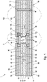
- a preferred embodiment of a printed circuit board 1 with an antenna structure 5 is shown, wherein the antenna structure 5 comprises an antenna design area 6 as well as an antenna cavity 60.
- the ground layer 10 comprises a first conducting metal layer 14, a second conducting metal layer 16 and an insulating layer 18, that is arranged and laminated between the conducting metal layers 14,16.
- a release layer 20 is positioned, as can be seen in more detail in Fig. 3A .
- Fig. 3A and Fig. 4A refer to details of individual stages of the first alternative manufacturing method as shown in Fig. 1 using an optional release layer 20 to obtain later on an antenna cavity with preferably exact outlines.
- a dielectric insulating layer 30 with an exterior side 31 of the dielectric insulating layer 30 and a dielectric insulating layer height 35 is attached on the ground layer 10.
- the release layer 20 On the exterior side 11 of the ground layer 10 that is partly covered by the release layer 20 the release layer 20 is arranged between the ground layer 10 and the dielectric insulating layer 30.
- a conducting layer 40 with a conducting layer height 45 is attached on the dielectric insulating layer 30 in a way that the dielectric insulating layer 30 is arranged between the conducting layer 40 and the ground layer 10.
- Fig. 3A shows the ground layer 10 in more detail.
- a release layer 20 is removable positioned on the exterior side 11 of the ground layer within an antenna subarea 12 .
- the position 22 of the release layer 20 on the exterior ground layer side 11 as well as the release layer shape 25 of the release layer 20 corresponds with the position and shape of the antenna cavity 60.
- Fig. 4A illustrates the step of attaching a dielectric insulating layer 30 and a conducting layer 40 on the exterior side of the ground layer 10 that is partly covered by the release layer 20 before laminating the layers to receive a first semi-finished product 50.
- the first semi-finished product 50 comprises an exterior side 51 of the first semi-finished product 50 that is formed by the conducting layer.
- an antenna cavity 60 is manufactured for example via a laser cutting and/or deep routing process throughout the conducting layer 40 as well as the dielectric insulating layer 30 with a cavity height 65 equal to the sum of the conducting layer height 45 and the dielectric insulating layer height 35.
- a cavity projection area 61 of the antenna cavity 60 corresponds to the release layer shape 25 and the release layer position 22 as of the release layer 20 on the antenna subarea 12.
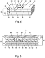
- Fig. 5 shows a ground-plane area 62 of the antenna cavity 60 that is made up of the release layer 20.
- the cut-out and/or shaped-out material of the conducting layer 40 and dielectric insulating layer 30 can easily be taken out of the cavity projection area 61 to form the antenna cavity 60.
- the antenna cavity 60 can be coated with a metal coating 66 on its side walls 67, 68 as is shown in Fig. 1 and can be seen in more detail also in Fig. 5 .
- a vent through-hole 69 can be drilled between the ground-plane area 62 of the antenna cavity 60 and an outer surface 99 of the printed circuit board 1.
- This vent through-hole 69 is manufactured as non-plated through hole and enhances pressure compensation between the interior of the antenna cavity 60 and the surrounding of the printed circuit board 1.
- a compound signal layer 70 with an exterior side 71 of the signal layer 70 is attached on the exterior side 51 of the first semi-finished product 50 that is made up of the conducting layer 40.
- the compound signal layer 70 covers the antenna cavity 60.
- a compound antenna layer 75 is received comprising a dielectric no-flow prepreg layer 76 and a conducting metal layer 78 forming the compound signal layer 70 as well as the conducting layer 40.
- solder masks 91, 92 are affixed on both exterior sides 81, 82 of the intermediate printed circuit board product 80 to apply structured solder layers 90 within recesses 95 of the solder masks 91, 92.
- the skilled person is perfectly acquainted with the technology how to apply solder layers as preparation for components that are later on mounted on the printed circuit board via soldering.
- the outer surfaces 99 are finished to receive a printed circuit board 1 with an antenna structure 5 as is illustrated in Fig. 1 .
- the antenna structure 5 and a digital processing area 105 each are marked by dotted lines.
- Fig. 1A shows in a sectional view a printed circuit board 1 obtained from the embodiment as shown in Fig. 1 with structured conducting paths of conducting layers 14, 16, 40, 78 that are connected by vias according to their electrical function.
- a surface-mounted signal processing unit 101 is already assembled within a digital processing area 105.
- Fig. 1A also an aerial view of the antenna design area 6 is inserted.
- the antenna design area 6 is arranged on an exterior side 71 of the compound signal layer 70 is illustrated as an insert surrounded by dotted lines that show the outer contour of the antenna cavity 60 beneath, which is the cavity projection area 61.
- a micro-via structure that is printed on the upper exterior side of the dielectric no-flow prepreg layer 76 is shown within the antenna design area 6. As can be seen the antenna stubs of the micro-via structure end in a distance to the cavity projection area 61.
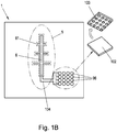
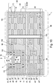
- Fig. 1B is a top view of a detail of Fig. 1A .
- a digital processing structure 100 is positioned within a digital processing area 105.
- the digital processing structure 100 comprises here a signal processing unit 101 with a radio frequency integrated circuit (RFIC) chip 102 that is already known in the art.
- the RFIC-chip 102 is mounted on the printed circuit board 1.
- the signal processing unit 101 is designed for analogue and digital signal processing of antenna signals and further comprises a radio frequency (RF) mixer that is integrated as a component within the RFIC chip 102.
- the RF mixer is used to convert a high-frequency antenna signal to a medium-frequency signal that can be processed further in the signal processing unit 101.
- the signal processing unit 101 also comprises at least one filter, AD converter, decoder, amplifier, memory unit and/or power supply unit.
- the signal processing unit 101 is connected via an antenna signal line 104 with the antenna structure 5, which is adapted for high frequency antenna signals.
- antenna signal line 104 For example here a microstrip line is used as antenna signal line 104.
- Fig. 1B illustrates that within an antenna structure 5 there is an antenna design area 6 realized on the upper exterior side 71 of the compound signal layer 70.
- the antenna design area 6 shows an antenna structure for example of a travelling wave antenna with a main line and several open stubs being arranged in a way that the open stubs end well before the side walls of the below antenna cavity 60.
- the below-lying antenna cavity 60 or the contour of its cavity projection area 61, respectively, is shown in Fig. 1B as dotdashed line.
- the distance between the antenna design area 6 and the cavity projection area 61 does not need to be a single, constant measure.
- An antenna signal line 104 connects the antenna design area 6 and the RFIC-chip 102 via solder pads 96 that are arranged here in a ball grid array (BGA) according to the position of respective interconnection pins 103 that are arranged on the bottom side of the RFIC-chip 102.
- the shown pins 103 are solder balls.
- BGA packages are used to permanently mount devices such as microprocessors.
- Fig. 1B shows the footprint of the ball grid array, while the RFIC-chip 102 is shown in a lifted position before being soldered with its pins 103 on the respective solder pads 96.
- Components and/or parts of the signal processing unit 101 may be embedded especially within the same laminated ground layer 10, laminated dielectric insulating layer 30, conducting layer 40 as well as compound signal layer 70 in a distance 125 in regard to the antenna cavity 60.
- the digital structure 100 comprises here also a plated through hole 120 passing through the intermediate printed circuit board product 80 from a first exterior side 81 of the intermediate printed circuit board product 80 to an opposite second exterior side 82. As shown exemplarily in Fig. 1 , the side walls within the through hole 120 are covered with a coating 66. Additionally the antenna cavity 60 is surrounded by several shielding vias 110 that are arranged here within the laminated ground layer 10, the dielectric insulating layer 30, the conducting layer 40 as well as the compound signal layer 70 each in a distance 115 in regard to the antenna cavity 60.
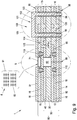
- Fig. 2 illustrates the several production steps to produce a printed circuit board 1 according to an alternative second inventive method without usage of a release layer.
- a signal processing unit 101 is already embedded within a digital processing area 105. Reference numbers are the same as in Figures 1 and 1A .
- a further dielectric insulating layer 30' and a further conducting layer 40' are shown that are stacked alternatingly on top of the preceding layers 30, 40.
- the printed circuit board 1 is shown with already structured conducting paths of conducting layers 14,16, 40, 40', 78 according to their electrical function.
- the plurality of layers include conductive planes with structured conducting paths that are connected by vias. Also the signal processing unit 101 is already assembled and contacted with the antenna design area 6 via an antenna signal line 104.
- the antenna signal line 104 is designed as short path within the conducting metal layer 78, thus on the same layer as the antenna contacts and the interconnection pins 6 of the embedded RFIC-chip 102 are positioned.
- Fig. 2 shows only a detail of a sequential layer build-up of a printed circuit board 1, further layers that are comprised in this build-up are indicated via dashed lines only.
- Fig. 3B and Fig. 4B refer to details of individual stages of the second alternative method of manufacture without using a release layer comparable with Fig. 2 .
- a ground layer 10 without release layer is shown.
- Fig. 4B illustrates in an isometric and partly sectional view the step of attaching a first dielectric insulating layer 30 and a first conducting layer 40 on the exterior side 11 of the ground layer 10 before optionally stacking up further dielectric insulating layers 30' and conducting layers 40' in an alternating arrangement. These further layers 30' and 40' are not shown in Fig. 4B .
- the stack of layers 10, 30, 40, 30', 40' is laminated to receive a first semi-finished product 50, wherein recesses 39, 39' within the dielectric insulating layers 30, 30' and respective recesses 49, 49' within the conducting layers 40, 40' are stacked in a coextensive way to form an antenna cavity 60.
- a first semi-finished product 50 as shown in Fig. 5 can be easily derived by laminating the respective layers 10, 30, 40.
- further layer arrangements like pairs of dielectric insulating layers 30' and conducting layers 40', that are stacked alternatingly, can be laminated together with the preceding layers to obtain a multi-layered semi-finished product 50.
- Fig. 7 shows in a top view a detail of an antenna structure 5 of another embodiment of an intermediate printed circuit board 1 according to the invention.
- Fig. 8 depicts a sectional view according to sectional plane A-A as marked in Fig. 7 .
- the antenna design area 6 has here a complex, tree-like shape.
- the respective antenna cavity 60 underneath has an enlarged shape comparable to that of the antenna design area 6.
- the cavity projection area 61 of the antenna cavity 60 is larger than the antenna design area 6.
- the antenna stubs of the micro-via structure end in a distance to the cavity projection area 61. It is emphasized that said distance between the antenna design area 6 and the cavity projection area 61 does not need to be a single, constant measure.
- the shape of the antenna cavity 60 beneath does not have to be in exact equidistance in regard to the micro-via structure of the antenna design area 6.
- the antenna is here attached to the dielectric no-flow prepreg layer 76.
- the cavity height 65 of the antenna cavity 60 can be adjusted depending on the number of stacked-up layers 30, 40.
- the antenna cavity 60 is made for example via a laser cutting process wherein the applicants' 2.5D technology is applied.
- Fig. 9 is a sectional view of another embodiment of a printed circuit board 1 according to the invention, comprising a surface-mounted signal processing unit 101 that is connected with the ground layer 10 of the printed circuit board 1 by through holes 120.
- the layer wise build-up as shown in Fig. 9 is the same as previously described in Figures 1 and 1A . Also the respective reference numbers are the same as previously used and refer to the same items.
- the conducting paths are already structured and are connected by vias.
- the interconnection pins 103 of a surface-mounted RFIC-chip 102 are connected within plated through holes 120 and solder pads 96 to the ground layer 10.
- the through holes 120 pass through all layers of the printed circuit board 1.
- antenna signal line 104 a microstrip line is used which is designed as short connection between the antenna structure 5 and the digital processing structure 100.
- Fig. 10 illustrates another alternative embodiment of a printed circuit board 1 according to the invention with a HDI (high-density interconnect) any-layer design.
- This embodiment includes a plurality of layers including conducting layers connected by vias.
- the electrical connections between the individual layers mainly consist of laser-drilled microvias.
- the main advantage of this technology is that all the layers can be freely interconnected. In general laser-drilled microvias electroplated with copper are used.
- This printed circuit board 1 is manufactured for example according to a sequential layer build-up (SBU).
- SBU sequential layer build-up
- manufacture is started with a core (double sided or an insulator), with conductive and dielectric layers formed one after the other on both sides of the board.
- This technology also allows blind vias to be created during the build-up process, and discrete or formed components to be embedded.
- the further dielectric insulating layer 30 and the further conducting layer 40 both have recesses 39, 49 that are in registry with the antenna cavity 60 beneath the compound signal layer 70.
- an antenna recess 150 is formed.
- usage of a low-flow material or no-flow material as further dielectric insulating layer 30 is preferred.
- the antenna recess 150 could also be manufactured via 2.5D technology developed by the applicant.
- side walls within the antenna recess 150 can be metallized and have for example a copper coating.
- shielding vias 110 are manufactured and are arranged within the printed circuit board product 1 in a distance 115 in regard to the antenna cavity 60. Further shielding vias 110 are arranged within the printed circuit board 1 close to the antenna recess 150.
- the lower part that is shown in Fig. 10 below the core material 130 As said before according to SBU technique applied for this manufacture, layer wise build-up is formed one after the other on both sides of the core material 130 simultaneously.
- the lower part which is indicated here as intermediate printed circuit board product 80' comprises a layer arrangement of insulating layers 30, 30', 30", 30'" and of conducting layers 40, 40', 40", 40''' that are attached accordingly.
- the multi-layer build up is laminated.
- Structured solder masks 91 are applied on both exterior sides of the multi-layer build-up.
- a vent through-hole 69 is manufactured between the ground-plane area of the cavity 60 and the lower exterior side of the multi-layer build-up.
- a pressure compensation can take place between the inside pressure within the air gap of the antenna cavity 60 and the surrounding pressure outside of the PCB.
- a plated through hole 120 is shown that runs through printed circuit board 1.
- Fig. 10 Not shown in Fig. 10 is the assembly of a RFIC-chip on already prepared solder pads 96 that are connected via a HF antenna signal line 104 to the antenna structure 5.
- the antenna signal line 104 is positioned on the upper side of the dielectric no-flow prepreg layer 76 and is structured together with the antenna design area 6 within the same manufacturing step.
- the RFIC-chip in this embodiment will be surface-mounted within the digital processing area 105 on the upper exterior side of the printed circuit board 1. Afterwards the outer surfaces 99 are finished to obtain a finished printed circuit board 1 with an antenna structure 5 according to the invention.
- further parts or components of the signal processing unit can be surface-mounted and/or embedded within the marked digital processing area 105.
- further antenna structures 5 comprising antenna cavities 60 that may be arranged within the upper part 80 and/or the lower part 80' of the printed circuit board 1.
Landscapes
- Engineering & Computer Science (AREA)
- Microelectronics & Electronic Packaging (AREA)
- Manufacturing & Machinery (AREA)
- Physics & Mathematics (AREA)
- Electromagnetism (AREA)
- Details Of Aerials (AREA)
- Waveguide Aerials (AREA)
- Production Of Multi-Layered Print Wiring Board (AREA)
Claims (20)
- Verfahren zum schichtweisen Herstellen eines Leiterplattenzwischenprodukts (80) mit einer Antennenstruktur (5), umfassend die folgenden Schritte:- Bereitstellen einer Erdungsschicht (10);- Optionales Anbringen einer Trennschicht (20) mit einer Trennschichtform (25) auf einer Außenseite (11) der Erdungsschicht (10), wobei die Trennschicht (20) auf einem Antennenteilbereich (12) der Außenseite (11) der Erdungsschicht (10) lösbar positioniert (22) ist;- Anbringen einer dielektrischen Isolierschicht (30) direkt auf einer Außenseite (11) der Erdungsschicht (10), die gegebenenfalls teilweise von der Trennschicht (20) bedeckt ist, wobei die Trennschicht (20) zwischen der Erdungsschicht (10) und der dielektrischen Isolierschicht (30) angeordnet ist;- Anbringen einer leitenden Schicht (40) direkt auf einer ersten Außenseite (31) der dielektrischen Isolierschicht (30) gegenüber der Erdungsschicht (10), wobei die dielektrische Isolierschicht (30) zwischen der leitenden Schicht (40) und der Erdungsschicht (10) angeordnet ist;- Schichtweises Laminieren der Erdungsschicht (10), der mindestens einen dielektrischen Isolierschicht (30, 30'), der mindestens einen leitenden Schicht (40, 40') und gegebenenfalls der Trennschicht (20) und- Optionales Anbringen einer Schichtanordnung auf einer ersten Außenseite (41) der leitenden Schicht (40), wobei die Schichtanordnung mindestens eine weitere dielektrische Isolierschicht (30', 30") und mindestens eine weitere leitende Schicht (40', 40") umfasst, wobei mindestens eine weitere dielektrische Isolierschicht (30') an der ersten Außenseite (41) der leitenden Schicht (40) angebracht ist und mindestens eine weitere leitende Schicht (40') an einer ersten Außenseite (31) der mindestens einen weiteren dielektrischen Isolierschicht (30', 30") angebracht ist, um ein erstes Halbfertigprodukt (50) zu erhalten;- Herstellen mindestens eines Antennenhohlraums (60) innerhalb des ersten Halbfertigprodukts (50) ausgehend von dessen Außenseite (51), der aus der mindestens einen leitenden Schicht (40, 40') gebildet ist und sich über mindestens eine leitende Schicht (40) sowie mindestens eine dielektrische Isolierschicht (30) erstreckt, mit einer Hohlraumhöhe (65), die gleich der Summe aus mindestens einer leitenden Schichthöhe (45) und mindestens einer dielektrischen Isolierschichthöhe (35) ist, wobei gegebenenfalls eine Hohlraumprojektionsfläche (61) der Trennschichtform (25) entspricht und auf dem von der Trennschicht (20) abgedeckten Antennenteilbereich (12) positioniert (22) ist und wobei eine Erdungsebenenfläche (62) des Hohlraums (60) von der Trennschicht (20) gebildet wird;- Optionales Beschichten (66) der Seitenwände (67, 68) innerhalb des Antennenhohlraums (60);- Anbringen einer Verbindungssignalschicht (70) auf der Außenseite (51), die aus der leitenden Schicht (40) des ersten Halbfertigprodukts (50) besteht, wobei die Verbindungssignalschicht (70) den Antennenhohlraum (60) abdeckt;- Laminieren des ersten Halbfertigprodukts (50) und der Verbindungssignalschicht (70), um ein Leiterplattenzwischenprodukt (80) zu erhalten.
- Verfahren zum schichtweisen Herstellen eines Leiterplattenzwischenprodukts (80) mit einer Antennenstruktur (5), umfassend die folgenden Schritte:- Bereitstellen einer Erdungsschicht (10);- Anbringen einer dielektrischen Isolierschicht (30) direkt auf einer Außenseite (11) der Erdungsschicht (10), wobei die dielektrische Isolierschicht (30) mindestens eine Ausnehmung (39) aufweist, die sich über die gesamte dielektrische Isolierschichthöhe (35) der dielektrischen Isolierschicht (30) erstreckt, und wobei die mindestens eine Ausnehmung (39) auf einem Antennenteilbereich (12) der Außenseite (11) der Erdungsschicht (10) positioniert ist;- Anbringen einer leitenden Schicht (40) direkt auf einer ersten Außenseite (31) der dielektrischen Isolierschicht (30) gegenüber der Erdungsschicht (10), wobei die dielektrische Isolierschicht (30) zwischen der leitenden Schicht (40) und der Erdungsschicht (10) angeordnet ist und wobei die leitende Schicht (40) vorzugsweise mindestens eine sich über die gesamte leitende Schichthöhe (45) der leitenden Schicht (40) erstreckende Ausnehmung (49) aufweist, die koextensiv zu der mindestens einen Ausnehmung (39) der dielektrischen Isolierschicht (30) angeordnet ist;- Schichtweises Laminieren der Erdungsschicht (10), der mindestens einen dielektrischen Isolierschicht (30) und der mindestens einen leitenden Schicht (40) und- Optionales Anbringen einer Schichtanordnung auf einer ersten Außenseite (41) der leitenden Schicht (40), wobei die Schichtanordnung mindestens eine weitere dielektrische Isolierschicht (30', 30") und mindestens eine weitere leitende Schicht (40', 40") umfasst, wobei mindestens eine weitere dielektrische Isolierschicht (30', 30") an der ersten Außenseite (41) der leitenden Schicht (40) angebracht ist und mindestens eine weitere leitende Schicht (40') an einer ersten Außenseite (31) der mindestens einen weiteren dielektrischen Isolierschicht (30') angebracht ist und wobei vorzugsweise mindestens eine weitere dielektrische Isolierschicht (30', 30") und mindestens eine weitere leitende Schicht (40', 40") mindestens eine Ausnehmung (39, 49) aufweist, die in Deckung mit mindestens einer der vorhergehenden Ausnehmungen (39, 49) sowie in Deckung mit einem Antennenteilbereich (12) auf der Außenseite (11) der Erdungsschicht (10) positioniert ist, um ein erstes Halbfertigprodukt (50) zu erhalten;- Erhalten mindestens eines Antennenhohlraums (60) innerhalb des ersten Halbfertigprodukts (50), ausgehend von dessen Außenseite (51), der aus der Ausnehmung (49) mindestens einer leitenden Schicht (40) sowie der koextensiven Ausnehmung (39) mindestens einer dielektrischen Isolierschicht (30) gebildet ist, der mindestens eine Antennenhohlraum (60) eine Hohlraumhöhe (65) aufweist, die gleich der Summe aus mindestens einer leitenden Schichthöhe (45) und mindestens einer dielektrischen Isolierschichthöhe (35) ist, wobei ein Hohlraumprojektionsbereich (65) des Antennenhohlraums (60) auf dem Antennenteilbereich (12) positioniert (22) ist;- Optionales Beschichten (66) der Seitenwände (67, 68) innerhalb des Antennenhohlraums (60);- Anbringen einer Verbindungssignalschicht (70) auf der Außenseite (51), die aus der leitenden Schicht (40) des ersten Halbfertigprodukts (50) besteht, wobei die Verbindungssignalschicht (70) den mindestens einen Antennenhohlraum (60) abdeckt;- Laminieren des ersten Halbfertigprodukts (50) und der Verbindungssignalschicht (70), um ein Leiterplattenzwischenprodukt (80) zu erhalten.
- Verfahren nach Anspruch 1 oder 2, dadurch gekennzeichnet, dass die Verbindungssignalschicht (70) eine dielektrische No-Flow-Prepreg-Schicht (76) und eine leitende Metallschicht (78) umfasst, die direkt an der dielektrischen No-Flow-Prepreg-Schicht (76) angebracht ist, wobei die dielektrische No-Flow-Prepreg-Schicht (76) an einer leitenden Schicht (40) des ersten Halbfertigprodukts (50) angebracht ist.
- Verfahren nach einem der Ansprüche 1 bis 3, dadurch gekennzeichnet, dass die Erdungsschicht (10) aus einer laminierten Verbindungsschicht besteht, die mindestens zwei leitende Metallschichten (14, 16) umfasst, die mit einer Isolierschicht (18) zwischen den mindestens zwei leitenden Metallschichten (14, 16) laminiert sind, wobei gegebenenfalls eine Schichtanordnung aus mindestens einer weiteren Isolierschicht (18') und mindestens einer weiteren leitenden Metallschicht (16') aufgestapelt und mit den vorhergehenden Schichten zu der laminierten Verbindungsschicht laminiert wird.
- Verfahren nach einem der Ansprüche 1 bis 4, dadurch gekennzeichnet, dass der Antennenhohlraum (60) ein Entlüftungsdurchlassloch (69) aufweist, das zwischen dem Erdungsebenenbereich (62) des Hohlraums (60) und einer Außenseite (82) des Leiterplattenzwischenprodukts (80) angeordnet ist.
- Verfahren nach einem der Ansprüche 1 bis 5, dadurch gekennzeichnet, dass der Antennenhohlraum (60) mit Abschirmvias (110) umgeben wird, die innerhalb der laminierten Erdungsschicht (10) und/oder mindestens einer dielektrischen Isolierschicht (30) und/oder mindestens einer leitenden Schicht (40) und/oder Verbindungssignalschicht (70) in einem Abstand (115) mit Bezug zum Antennenhohlraum (60) angeordnet sind.
- Verfahren nach einem der Ansprüche 1 bis 6, dadurch gekennzeichnet, dass die Antennenstruktur (5) einen Antennendesignbereich (6) umfasst, der auf einer Außenseite (71) der Verbindungssignalschicht (70) angeordnet ist.
- Verfahren nach einem der Ansprüche 1 bis 7, dadurch gekennzeichnet, dass ein digitaler Verarbeitungsbereich (105) mit einer digitalen Verarbeitungsstruktur (100), die mindestens eine Signalverarbeitungseinheit (101) umfasst, auf dem Leiterplattenzwischenprodukt (80) in einem Abstand (125) zum Antennenhohlraum (60) angebracht oder darin eingebettet ist, wobei die Signalverarbeitungseinheit (101) über mindestens eine Antennensignalleitung (104) mit der Antennenstruktur (5) verbunden ist und zur analogen und digitalen Signalverarbeitung von Antennensignalen ausgelegt ist.
- Verfahren nach einem der Ansprüche 1 bis 8, dadurch gekennzeichnet, dass Lötmasken (91, 92) auf einer oder beiden Außenseiten (81, 82) eines Leiterplattenzwischenprodukts (80) oder auf einer oder beiden Außenseiten (81, 82) von mindestens zwei zuvor miteinander verbundenen und gestapelten Leiterplattenzwischenprodukten (80) aufgebracht werden.
- Leiterplattenzwischenprodukt (80) mit einer Antennenstruktur (5), dadurch gekennzeichnet, dass mindestens ein Antennenhohlraum (60) innerhalb eines ersten Halbfertigprodukts (50) angeordnet ist, das mindestens eine Erdungsschicht (10) umfasst, mindestens eine dielektrische Isolierschicht (30), die direkt an der Erdungsschicht (10) angebracht ist, und mindestens eine leitende Schicht (40), die direkt an der dielektrischen Isolierschicht (30) gegenüber der Erdungsschicht (10) in einer Weise angebracht ist, dass die mindestens eine dielektrische Isolierschicht (30) in direktem Kontakt zwischen der mindestens einen leitenden Schicht (40) und der Erdungsschicht (10) angeordnet ist, wobei die Erdungsschicht (10), die mindestens eine dielektrische Isolierschicht (30) und die mindestens eine leitende Schicht (40) laminiert sind, und wobei der Antennenhohlraum (60) die Erdungsschicht (10) entlang eines Erdungsebenenbereichs (62) berührt und sich durch die mindestens eine leitende Schicht (40) sowie die mindestens eine dielektrische Isolierschicht (30) mit einer Hohlraumhöhe (65) erstreckt, die gleich der Summe der Höhe der mindestens einen leitenden Schicht (45) und der Höhe der mindestens einen dielektrischen Isolierschicht (35) ist, wobei auf der leitenden Schicht (40) des den Antennenhohlraum (60) abdeckenden ersten Halbfertigprodukts (50) eine Verbindungssignalschicht (70) aufgebracht ist, und das erste Halbfertigprodukt (50) und die Verbindungssignalschicht (70) laminiert sind, wobei der Antennenhohlraum (60) mit Abschirmdurchkontaktierungen (110) umgeben ist, die innerhalb der Erdungsschicht (10) und/oder dielektrischen Isolierschicht (30) und/oder leitenden Schicht (40) und/oder Verbindungssignalschicht (70) in einem Abstand (115) zum Antennenhohlraum (60) angeordnet sind.
- Leiterplattenzwischenprodukt (80) nach Anspruch 10, dadurch gekennzeichnet, dass die Verbindungssignalschicht (70) eine dielektrische No-Flow-Prepreg-Schicht (76) und eine leitende Metallschicht (78) umfasst, die direkt an der dielektrischen No-Flow-Prepreg-Schicht (76) angebracht ist, wobei die dielektrische No-Flow-Prepreg-Schicht (76) an einer leitenden Schicht (40) des ersten Halbfertigprodukts (50) angebracht ist.
- Leiterplattenzwischenprodukt (80) nach Anspruch 10 oder 11, dadurch gekennzeichnet, dass ein digitaler Verarbeitungsbereich (105) mit einer digitalen Verarbeitungsstruktur (100), die mindestens eine Signalverarbeitungseinheit (101) umfasst, auf dem Leiterplattenzwischenprodukt (80) in einem Abstand (125) zum Antennenhohlraum (60) angebracht oder darin eingebettet ist, wobei die Verarbeitungseinheit (101) über mindestens eine Antennensignalleitung (104) mit der Antennenstruktur (5) verbunden ist und zur analogen und digitalen Signalverarbeitung von Antennensignalen ausgelegt ist.
- Leiterplattenzwischenprodukt (80) nach einem der Ansprüche 10 bis 12, dadurch gekennzeichnet, dass mindestens ein Antennenhohlraum (60) ein vom Erdungsebenenbereich (62) ausgehendes und durch die laminierte Erdungsschicht (10) verlaufendes Entlüftungsdurchlassloch (69) aufweist.
- Leiterplattenzwischenprodukt (80) nach einem der Ansprüche 10 bis 13, dadurch gekennzeichnet, dass die Antennenstruktur (5) einen Antennendesignbereich (6) aufweist, der auf einer Außenseite (71) der Verbindungssignalschicht (70) angeordnet ist, vorzugsweise ist der Antennendesignbereich (6) oberhalb des Antennenhohlraums (60) angeordnet, besonders bevorzugt ist der Antennendesignbereich (6) innerhalb eines Hohlraumprojektionsbereichs (61) als Außenkontur des darunterliegenden Antennenhohlraums (60) angeordnet.
- Leiterplattenzwischenprodukt (80) nach Anspruch 14, dadurch gekennzeichnet, dass der Antennendesignbereich (6) auf der Außenseite (71) der Verbindungssignalschicht (70) innerhalb einer Antennenausnehmung (150) unterhalb einer Außenseite (81, 82) des Leiterplattenzwischenprodukts (80) angeordnet ist.
- Leiterplattenzwischenprodukt (80) nach einem der Ansprüche 10 bis 15, dadurch gekennzeichnet, dass die den Antennenhohlraum (60) umgebenden Abschirmvias (110) innerhalb von Schichten oberhalb und/oder seitlich und/oder unterhalb des Antennenhohlraums (60) angeordnet sind.
- Leiterplattenzwischenprodukt (80) nach einem der Ansprüche 10 bis 16, dadurch gekennzeichnet, dass der Antennenhohlraum (60) an seinen Seitenwänden (67, 68) mit einer Metallbeschichtung (66) versehen ist.
- Leiterplatte (1) mit einer Antennenstruktur (5), die mindestens ein Leiterplattenzwischenprodukt (80) nach einem der Ansprüche 10 bis 17 umfasst, dadurch gekennzeichnet, dass eine Lötmaske (91, 92) auf einer oder beiden Außenseiten (81, 82) eines Leiterplattenzwischenprodukts (80) oder auf einer oder beiden Außenseiten (81, 82) von mindestens zwei zuvor miteinander verbundenen und gestapelten Leiterplattenzwischenprodukten (80) aufgebracht ist.
- Leiterplatte (1) nach Anspruch 18, dadurch gekennzeichnet, dass die Antennenstruktur (5) einen Antennendesignbereich (6) umfasst, der auf einer Außenseite (71) der Verbindungssignalschicht (70) angeordnet ist, wobei vorzugsweise der Antennendesignbereich (6) oberhalb des Antennenhohlraums (60) angeordnet ist, wobei besonders bevorzugt der Antennendesignbereich (6) innerhalb eines Hohlraumprojektionsbereichs (61) als Außenkontur des darunter liegenden Antennenhohlraums (60) angeordnet ist.
- Leiterplattenprodukt (1) nach Anspruch 19, dadurch gekennzeichnet, dass der Antennendesignbereich (6) auf der Außenseite (71) der Verbindungssignalschicht (70) innerhalb einer Antennenausnehmung (150) unterhalb einer Außenfläche (99) der Leiterplatte (1) angeordnet ist.
Applications Claiming Priority (1)
| Application Number | Priority Date | Filing Date | Title |
|---|---|---|---|
| EP16157837.2A EP3211976A1 (de) | 2016-02-29 | 2016-02-29 | Leiterplatte mit antennenstruktur und verfahren zu dessen herstellung |
Publications (2)
| Publication Number | Publication Date |
|---|---|
| EP3211977A1 EP3211977A1 (de) | 2017-08-30 |
| EP3211977B1 true EP3211977B1 (de) | 2021-06-16 |
Family
ID=55443183
Family Applications (2)
| Application Number | Title | Priority Date | Filing Date |
|---|---|---|---|
| EP16157837.2A Withdrawn EP3211976A1 (de) | 2016-02-29 | 2016-02-29 | Leiterplatte mit antennenstruktur und verfahren zu dessen herstellung |
| EP17158161.4A Active EP3211977B1 (de) | 2016-02-29 | 2017-02-27 | Leiterplatte mit antennenstruktur und verfahren zu dessen herstellung |
Family Applications Before (1)
| Application Number | Title | Priority Date | Filing Date |
|---|---|---|---|
| EP16157837.2A Withdrawn EP3211976A1 (de) | 2016-02-29 | 2016-02-29 | Leiterplatte mit antennenstruktur und verfahren zu dessen herstellung |
Country Status (3)
| Country | Link |
|---|---|
| US (1) | US10490887B2 (de) |
| EP (2) | EP3211976A1 (de) |
| CN (1) | CN107135616B (de) |
Families Citing this family (38)
| Publication number | Priority date | Publication date | Assignee | Title |
|---|---|---|---|---|
| US20160301241A1 (en) * | 2015-04-09 | 2016-10-13 | Samsung Electro-Mechanics Co., Ltd. | Wireless power receiver and power supply apparatus using the same |
| KR102450606B1 (ko) * | 2015-09-25 | 2022-10-05 | 주식회사 위츠 | 무선 전력 수신 장치 및 그를 이용한 전원 공급 장치 |
| DE102016212129B4 (de) * | 2016-07-04 | 2022-05-19 | Schweizer Electronic Ag | Hochfrequenz-Sende-/Empfangselement und Verfahren zur Herstellung eines Hochfrequenz-Sende-/Empfangselementes |
| US20180294569A1 (en) * | 2017-04-07 | 2018-10-11 | Skyworks Solutions, Inc. | Radio-frequency module with integrated shield layer antenna and integrated cavity-based antenna |
| US11069978B2 (en) * | 2017-04-07 | 2021-07-20 | Skyworks Solutions, Inc. | Method of manufacturing a radio-frequency module with a conformal shield antenna |
| KR102265616B1 (ko) * | 2017-04-26 | 2021-06-16 | 삼성전자 주식회사 | 안테나 장치 및 이를 포함하는 전자 장치 |
| TWI678772B (zh) * | 2017-04-28 | 2019-12-01 | 矽品精密工業股份有限公司 | 電子封裝件及其製法 |
| US10206286B2 (en) * | 2017-06-26 | 2019-02-12 | Infineon Technologies Austria Ag | Embedding into printed circuit board with drilling |
| US10921420B2 (en) * | 2017-10-04 | 2021-02-16 | Infineon Technologies Ag | Dual-sided radar systems and methods of formation thereof |
| US11169250B2 (en) * | 2017-10-27 | 2021-11-09 | Mediatek Inc. | Radar module incorporated with a pattern-shaping device |
| CN109926298B (zh) * | 2017-12-18 | 2021-01-05 | 深圳先进技术研究院 | 一种模式转换超声换能器及其制造方法 |
| KR101938106B1 (ko) * | 2018-01-25 | 2019-01-14 | 주식회사 기가레인 | 선폭 축소형 연성회로기판 |
| US11233310B2 (en) * | 2018-01-29 | 2022-01-25 | The Boeing Company | Low-profile conformal antenna |
| CN108281739B (zh) * | 2018-03-27 | 2020-05-22 | 深圳市华扬通信技术有限公司 | 一种微带滤波器 |
| WO2019183732A1 (en) * | 2018-03-28 | 2019-10-03 | Mendelson Aaron Daniel | System and method for tracking users or objects and providing associated data or features corresponding thereto |
| CN110392134B (zh) * | 2018-04-20 | 2021-07-27 | Oppo广东移动通信有限公司 | 一种显示屏组件及电子设备 |
| US11487984B2 (en) * | 2018-06-11 | 2022-11-01 | Konica Minolta, Inc. | Contactlessly readable tag, method for manufacturing contactlessly readable tag, identification device, and identification information determination system |
| US11283486B1 (en) * | 2018-06-25 | 2022-03-22 | Hrl Laboratories, Llc | Mechanically actuated magnetostrictive transmitter |
| EP3859877B1 (de) * | 2018-10-19 | 2023-10-04 | Huawei Technologies Co., Ltd. | Antennenverpackungsstruktur und herstellungsverfahren dafür |
| CN109788644A (zh) * | 2019-03-25 | 2019-05-21 | 浙江万正电子科技有限公司 | 具有安装槽的局部镶嵌高频材料多层线路板及其制作方法 |
| CN110113863B (zh) * | 2019-05-09 | 2024-04-19 | 武汉精立电子技术有限公司 | 一种具有静电防护功能的pcb板 |
| CN112151459B (zh) * | 2019-06-26 | 2023-03-24 | 庆鼎精密电子(淮安)有限公司 | 封装电路结构及其制作方法 |
| US11127697B2 (en) * | 2019-07-10 | 2021-09-21 | Advanced Semiconductor Engineering, Inc. | Semiconductor device and method of manufacturing the same |
| KR102268382B1 (ko) * | 2019-11-20 | 2021-06-23 | 삼성전기주식회사 | 칩 안테나 모듈 |
| KR102913200B1 (ko) * | 2019-12-10 | 2026-01-15 | 엘지이노텍 주식회사 | 카메라 레이더 복합장치 |
| KR102880997B1 (ko) * | 2020-03-02 | 2025-11-04 | 삼성전기주식회사 | 인쇄회로기판 및 이를 포함하는 모듈 |
| CN111638813B (zh) * | 2020-06-03 | 2023-06-30 | 京东方科技集团股份有限公司 | 一种显示装置及其制造方法 |
| KR102864054B1 (ko) * | 2020-10-23 | 2025-09-24 | 삼성전자주식회사 | 인터포저를 포함하는 안테나 구조 및 이를 포함하는 전자 장치. |
| CN121568291A (zh) * | 2020-12-21 | 2026-02-24 | 3M创新有限公司 | 贴附了3d成型的电磁屏蔽膜的电路板、可3d成型的电磁屏蔽膜和3d成型的电磁屏蔽膜 |
| WO2022153275A1 (en) * | 2021-01-18 | 2022-07-21 | Vayyar Imaging Ltd. | Systems and methods for improving high frequency transmission in printed circuit boards |
| US12424716B2 (en) * | 2021-06-22 | 2025-09-23 | Intel Corporation | RF filters and multiplexers manufactured in the core of a package substrate using glass core technology |
| US20220407216A1 (en) * | 2021-06-22 | 2022-12-22 | Intel Corporation | In-package mmwave antennas and launchers using glass core technology |
| CN114340215A (zh) * | 2021-12-15 | 2022-04-12 | 昆山沪利微电有限公司 | 一种信号损耗小的4d车载雷达pcb板及其制作方法 |
| CN119678660A (zh) * | 2022-08-09 | 2025-03-21 | 昕诺飞控股有限公司 | 具有平面天线的混合pcb |
| CN116095943B (zh) * | 2022-12-19 | 2024-04-16 | 深圳市金晟达电子技术有限公司 | 一种多层阻抗hdi线路板 |
| CN115835484B (zh) * | 2022-12-30 | 2026-04-28 | 维沃移动通信有限公司 | 电路板及电子设备 |
| CN120530529A (zh) * | 2023-03-23 | 2025-08-22 | 深圳引望智能技术有限公司 | 印刷电路板中毫米波射频信号的自上而下空气波导 |
| CN116315644A (zh) * | 2023-04-21 | 2023-06-23 | 北京小米移动软件有限公司 | 天线及电子设备 |
Family Cites Families (12)
| Publication number | Priority date | Publication date | Assignee | Title |
|---|---|---|---|---|
| US5444453A (en) | 1993-02-02 | 1995-08-22 | Ball Corporation | Microstrip antenna structure having an air gap and method of constructing same |
| JPH08111609A (ja) | 1994-10-11 | 1996-04-30 | Murata Mfg Co Ltd | アンテナ装置 |
| US6131279A (en) * | 1998-01-08 | 2000-10-17 | International Business Machines Corporation | Integrated manufacturing packaging process |
| JP2002151911A (ja) | 2000-11-16 | 2002-05-24 | Matsushita Electric Ind Co Ltd | 高周波機器 |
| KR20050010549A (ko) | 2003-07-21 | 2005-01-28 | 엘지전자 주식회사 | Uwb 통신용 초소형 안테나 |
| US8101868B2 (en) * | 2005-10-14 | 2012-01-24 | Ibiden Co., Ltd. | Multilayered printed circuit board and method for manufacturing the same |
| EP2022133A4 (de) | 2006-05-04 | 2009-08-05 | Georgia Tech Res Inst | Modul-, filter- und antennentechnologie für drahtlose millimeterwellen-multi-gigabits-systeme |
| WO2008102950A1 (en) | 2007-02-22 | 2008-08-28 | Amotech Co., Ltd. | Internal antenna with air gap |
| AT12322U1 (de) * | 2009-01-27 | 2012-03-15 | Dcc Dev Circuits & Components Gmbh | Verfahren zur herstellung einer mehrlagigen leiterplatte, haftverhinderungsmaterial sowie mehrlagige leiterplatte und verwendung eines derartigen verfahrens |
| US8674885B2 (en) | 2010-08-31 | 2014-03-18 | Siklu Communication ltd. | Systems for interfacing waveguide antenna feeds with printed circuit boards |
| US8988299B2 (en) * | 2011-02-17 | 2015-03-24 | International Business Machines Corporation | Integrated antenna for RFIC package applications |
| TWI473552B (zh) | 2012-11-21 | 2015-02-11 | 欣興電子股份有限公司 | 具有元件設置區之基板結構及其製程 |
-
2016
- 2016-02-29 EP EP16157837.2A patent/EP3211976A1/de not_active Withdrawn
-
2017
- 2017-02-23 US US15/440,296 patent/US10490887B2/en active Active
- 2017-02-27 EP EP17158161.4A patent/EP3211977B1/de active Active
- 2017-02-28 CN CN201710115309.9A patent/CN107135616B/zh active Active
Non-Patent Citations (1)
| Title |
|---|
| None * |
Also Published As
| Publication number | Publication date |
|---|---|
| US10490887B2 (en) | 2019-11-26 |
| CN107135616A (zh) | 2017-09-05 |
| CN107135616B (zh) | 2020-04-17 |
| EP3211976A1 (de) | 2017-08-30 |
| EP3211977A1 (de) | 2017-08-30 |
| US20170250466A1 (en) | 2017-08-31 |
Similar Documents
| Publication | Publication Date | Title |
|---|---|---|
| EP3211977B1 (de) | Leiterplatte mit antennenstruktur und verfahren zu dessen herstellung | |
| EP3579334B1 (de) | Hf-funktionalität und abschirmung gegen elektromagnetische strahlung in einem komponententräger | |
| US10991674B2 (en) | Electronic assembly and electronic system with impedance matched interconnect structures | |
| US20150022982A1 (en) | Wiring board and method for manufacturing the same | |
| US20060017152A1 (en) | Heterogeneous organic laminate stack ups for high frequency applications | |
| CN103367269B (zh) | 用于射频应用的隔离混合基板 | |
| CN109309276B (zh) | 部件承载件的腔体中位于高频电介质上的天线结构 | |
| US20130170154A1 (en) | Printed circuit board having embedded capacitor and method of manufacturing the same | |
| US20110122041A1 (en) | Planar antenna | |
| CN112216673B (zh) | 部件承载件、制造部件承载件的方法及使用方法 | |
| US11527807B2 (en) | Electronic device having first and second component carrier parts with cut-outs therein and adhesively joined to form a cavity that supports an electronic component therein | |
| KR102518174B1 (ko) | 전자 소자 모듈 | |
| US12489205B2 (en) | Antenna layer structures separated by fluid-filled cavity, an antenna inlay, and a component carrier | |
| US12279369B2 (en) | Electrically connected component carrier stacks with respective cavities and method of manufacturing the same | |
| JP6725378B2 (ja) | アンテナモジュール | |
| JP2021078003A (ja) | 無線モジュール | |
| CN121844446A (zh) | 具有天线和被屏蔽的腔的部件承载件 |
Legal Events
| Date | Code | Title | Description |
|---|---|---|---|
| PUAI | Public reference made under article 153(3) epc to a published international application that has entered the european phase |
Free format text: ORIGINAL CODE: 0009012 |
|
| STAA | Information on the status of an ep patent application or granted ep patent |
Free format text: STATUS: THE APPLICATION HAS BEEN PUBLISHED |
|
| AK | Designated contracting states |
Kind code of ref document: A1 Designated state(s): AL AT BE BG CH CY CZ DE DK EE ES FI FR GB GR HR HU IE IS IT LI LT LU LV MC MK MT NL NO PL PT RO RS SE SI SK SM TR |
|
| AX | Request for extension of the european patent |
Extension state: BA ME |
|
| STAA | Information on the status of an ep patent application or granted ep patent |
Free format text: STATUS: REQUEST FOR EXAMINATION WAS MADE |
|
| 17P | Request for examination filed |
Effective date: 20180226 |
|
| RBV | Designated contracting states (corrected) |
Designated state(s): AL AT BE BG CH CY CZ DE DK EE ES FI FR GB GR HR HU IE IS IT LI LT LU LV MC MK MT NL NO PL PT RO RS SE SI SK SM TR |
|
| GRAP | Despatch of communication of intention to grant a patent |
Free format text: ORIGINAL CODE: EPIDOSNIGR1 |
|
| STAA | Information on the status of an ep patent application or granted ep patent |
Free format text: STATUS: GRANT OF PATENT IS INTENDED |
|
| RIC1 | Information provided on ipc code assigned before grant |
Ipc: H01Q 19/10 20060101ALN20201116BHEP Ipc: H01Q 1/38 20060101ALI20201116BHEP Ipc: H05K 3/46 20060101AFI20201116BHEP |
|
| INTG | Intention to grant announced |
Effective date: 20201202 |
|
| RIC1 | Information provided on ipc code assigned before grant |
Ipc: H01Q 19/10 20060101ALN20201120BHEP Ipc: H05K 3/46 20060101AFI20201120BHEP Ipc: H01Q 1/38 20060101ALI20201120BHEP |
|
| GRAS | Grant fee paid |
Free format text: ORIGINAL CODE: EPIDOSNIGR3 |
|
| GRAA | (expected) grant |
Free format text: ORIGINAL CODE: 0009210 |
|
| STAA | Information on the status of an ep patent application or granted ep patent |
Free format text: STATUS: THE PATENT HAS BEEN GRANTED |
|
| AK | Designated contracting states |
Kind code of ref document: B1 Designated state(s): AL AT BE BG CH CY CZ DE DK EE ES FI FR GB GR HR HU IE IS IT LI LT LU LV MC MK MT NL NO PL PT RO RS SE SI SK SM TR |
|
| REG | Reference to a national code |
Ref country code: GB Ref legal event code: FG4D |
|
| REG | Reference to a national code |
Ref country code: CH Ref legal event code: EP |
|
| REG | Reference to a national code |
Ref country code: DE Ref legal event code: R096 Ref document number: 602017040253 Country of ref document: DE |
|
| REG | Reference to a national code |
Ref country code: AT Ref legal event code: REF Ref document number: 1403427 Country of ref document: AT Kind code of ref document: T Effective date: 20210715 |
|
| REG | Reference to a national code |
Ref country code: IE Ref legal event code: FG4D |
|
| REG | Reference to a national code |
Ref country code: LT Ref legal event code: MG9D |
|
| PG25 | Lapsed in a contracting state [announced via postgrant information from national office to epo] |
Ref country code: HR Free format text: LAPSE BECAUSE OF FAILURE TO SUBMIT A TRANSLATION OF THE DESCRIPTION OR TO PAY THE FEE WITHIN THE PRESCRIBED TIME-LIMIT Effective date: 20210616 Ref country code: BG Free format text: LAPSE BECAUSE OF FAILURE TO SUBMIT A TRANSLATION OF THE DESCRIPTION OR TO PAY THE FEE WITHIN THE PRESCRIBED TIME-LIMIT Effective date: 20210916 Ref country code: FI Free format text: LAPSE BECAUSE OF FAILURE TO SUBMIT A TRANSLATION OF THE DESCRIPTION OR TO PAY THE FEE WITHIN THE PRESCRIBED TIME-LIMIT Effective date: 20210616 Ref country code: LT Free format text: LAPSE BECAUSE OF FAILURE TO SUBMIT A TRANSLATION OF THE DESCRIPTION OR TO PAY THE FEE WITHIN THE PRESCRIBED TIME-LIMIT Effective date: 20210616 |
|
| REG | Reference to a national code |
Ref country code: AT Ref legal event code: MK05 Ref document number: 1403427 Country of ref document: AT Kind code of ref document: T Effective date: 20210616 |
|
| REG | Reference to a national code |
Ref country code: NL Ref legal event code: MP Effective date: 20210616 |
|
| PG25 | Lapsed in a contracting state [announced via postgrant information from national office to epo] |
Ref country code: LV Free format text: LAPSE BECAUSE OF FAILURE TO SUBMIT A TRANSLATION OF THE DESCRIPTION OR TO PAY THE FEE WITHIN THE PRESCRIBED TIME-LIMIT Effective date: 20210616 Ref country code: GR Free format text: LAPSE BECAUSE OF FAILURE TO SUBMIT A TRANSLATION OF THE DESCRIPTION OR TO PAY THE FEE WITHIN THE PRESCRIBED TIME-LIMIT Effective date: 20210917 Ref country code: NO Free format text: LAPSE BECAUSE OF FAILURE TO SUBMIT A TRANSLATION OF THE DESCRIPTION OR TO PAY THE FEE WITHIN THE PRESCRIBED TIME-LIMIT Effective date: 20210916 Ref country code: SE Free format text: LAPSE BECAUSE OF FAILURE TO SUBMIT A TRANSLATION OF THE DESCRIPTION OR TO PAY THE FEE WITHIN THE PRESCRIBED TIME-LIMIT Effective date: 20210616 Ref country code: RS Free format text: LAPSE BECAUSE OF FAILURE TO SUBMIT A TRANSLATION OF THE DESCRIPTION OR TO PAY THE FEE WITHIN THE PRESCRIBED TIME-LIMIT Effective date: 20210616 |
|
| PG25 | Lapsed in a contracting state [announced via postgrant information from national office to epo] |
Ref country code: ES Free format text: LAPSE BECAUSE OF FAILURE TO SUBMIT A TRANSLATION OF THE DESCRIPTION OR TO PAY THE FEE WITHIN THE PRESCRIBED TIME-LIMIT Effective date: 20210616 Ref country code: NL Free format text: LAPSE BECAUSE OF FAILURE TO SUBMIT A TRANSLATION OF THE DESCRIPTION OR TO PAY THE FEE WITHIN THE PRESCRIBED TIME-LIMIT Effective date: 20210616 Ref country code: PT Free format text: LAPSE BECAUSE OF FAILURE TO SUBMIT A TRANSLATION OF THE DESCRIPTION OR TO PAY THE FEE WITHIN THE PRESCRIBED TIME-LIMIT Effective date: 20211018 Ref country code: RO Free format text: LAPSE BECAUSE OF FAILURE TO SUBMIT A TRANSLATION OF THE DESCRIPTION OR TO PAY THE FEE WITHIN THE PRESCRIBED TIME-LIMIT Effective date: 20210616 Ref country code: EE Free format text: LAPSE BECAUSE OF FAILURE TO SUBMIT A TRANSLATION OF THE DESCRIPTION OR TO PAY THE FEE WITHIN THE PRESCRIBED TIME-LIMIT Effective date: 20210616 Ref country code: CZ Free format text: LAPSE BECAUSE OF FAILURE TO SUBMIT A TRANSLATION OF THE DESCRIPTION OR TO PAY THE FEE WITHIN THE PRESCRIBED TIME-LIMIT Effective date: 20210616 Ref country code: AT Free format text: LAPSE BECAUSE OF FAILURE TO SUBMIT A TRANSLATION OF THE DESCRIPTION OR TO PAY THE FEE WITHIN THE PRESCRIBED TIME-LIMIT Effective date: 20210616 Ref country code: SM Free format text: LAPSE BECAUSE OF FAILURE TO SUBMIT A TRANSLATION OF THE DESCRIPTION OR TO PAY THE FEE WITHIN THE PRESCRIBED TIME-LIMIT Effective date: 20210616 Ref country code: SK Free format text: LAPSE BECAUSE OF FAILURE TO SUBMIT A TRANSLATION OF THE DESCRIPTION OR TO PAY THE FEE WITHIN THE PRESCRIBED TIME-LIMIT Effective date: 20210616 |
|
| PG25 | Lapsed in a contracting state [announced via postgrant information from national office to epo] |
Ref country code: PL Free format text: LAPSE BECAUSE OF FAILURE TO SUBMIT A TRANSLATION OF THE DESCRIPTION OR TO PAY THE FEE WITHIN THE PRESCRIBED TIME-LIMIT Effective date: 20210616 |
|
| REG | Reference to a national code |
Ref country code: DE Ref legal event code: R097 Ref document number: 602017040253 Country of ref document: DE |
|
| PLBE | No opposition filed within time limit |
Free format text: ORIGINAL CODE: 0009261 |
|
| STAA | Information on the status of an ep patent application or granted ep patent |
Free format text: STATUS: NO OPPOSITION FILED WITHIN TIME LIMIT |
|
| PG25 | Lapsed in a contracting state [announced via postgrant information from national office to epo] |
Ref country code: DK Free format text: LAPSE BECAUSE OF FAILURE TO SUBMIT A TRANSLATION OF THE DESCRIPTION OR TO PAY THE FEE WITHIN THE PRESCRIBED TIME-LIMIT Effective date: 20210616 |
|
| 26N | No opposition filed |
Effective date: 20220317 |
|
| PG25 | Lapsed in a contracting state [announced via postgrant information from national office to epo] |
Ref country code: AL Free format text: LAPSE BECAUSE OF FAILURE TO SUBMIT A TRANSLATION OF THE DESCRIPTION OR TO PAY THE FEE WITHIN THE PRESCRIBED TIME-LIMIT Effective date: 20210616 |
|
| PG25 | Lapsed in a contracting state [announced via postgrant information from national office to epo] |
Ref country code: IT Free format text: LAPSE BECAUSE OF FAILURE TO SUBMIT A TRANSLATION OF THE DESCRIPTION OR TO PAY THE FEE WITHIN THE PRESCRIBED TIME-LIMIT Effective date: 20210616 |
|
| PG25 | Lapsed in a contracting state [announced via postgrant information from national office to epo] |
Ref country code: MC Free format text: LAPSE BECAUSE OF FAILURE TO SUBMIT A TRANSLATION OF THE DESCRIPTION OR TO PAY THE FEE WITHIN THE PRESCRIBED TIME-LIMIT Effective date: 20210616 |
|
| REG | Reference to a national code |
Ref country code: CH Ref legal event code: PL |
|
| REG | Reference to a national code |
Ref country code: BE Ref legal event code: MM Effective date: 20220228 |
|
| GBPC | Gb: european patent ceased through non-payment of renewal fee |
Effective date: 20220227 |
|
| PG25 | Lapsed in a contracting state [announced via postgrant information from national office to epo] |
Ref country code: LU Free format text: LAPSE BECAUSE OF NON-PAYMENT OF DUE FEES Effective date: 20220227 |
|
| PG25 | Lapsed in a contracting state [announced via postgrant information from national office to epo] |
Ref country code: LI Free format text: LAPSE BECAUSE OF NON-PAYMENT OF DUE FEES Effective date: 20220228 Ref country code: IE Free format text: LAPSE BECAUSE OF NON-PAYMENT OF DUE FEES Effective date: 20220227 Ref country code: GB Free format text: LAPSE BECAUSE OF NON-PAYMENT OF DUE FEES Effective date: 20220227 Ref country code: CH Free format text: LAPSE BECAUSE OF NON-PAYMENT OF DUE FEES Effective date: 20220228 |
|
| PG25 | Lapsed in a contracting state [announced via postgrant information from national office to epo] |
Ref country code: BE Free format text: LAPSE BECAUSE OF NON-PAYMENT OF DUE FEES Effective date: 20220228 |
|
| P01 | Opt-out of the competence of the unified patent court (upc) registered |
Effective date: 20230526 |
|
| PG25 | Lapsed in a contracting state [announced via postgrant information from national office to epo] |
Ref country code: HU Free format text: LAPSE BECAUSE OF FAILURE TO SUBMIT A TRANSLATION OF THE DESCRIPTION OR TO PAY THE FEE WITHIN THE PRESCRIBED TIME-LIMIT; INVALID AB INITIO Effective date: 20170227 |
|
| PG25 | Lapsed in a contracting state [announced via postgrant information from national office to epo] |
Ref country code: MK Free format text: LAPSE BECAUSE OF FAILURE TO SUBMIT A TRANSLATION OF THE DESCRIPTION OR TO PAY THE FEE WITHIN THE PRESCRIBED TIME-LIMIT Effective date: 20210616 Ref country code: CY Free format text: LAPSE BECAUSE OF FAILURE TO SUBMIT A TRANSLATION OF THE DESCRIPTION OR TO PAY THE FEE WITHIN THE PRESCRIBED TIME-LIMIT Effective date: 20210616 |
|
| PG25 | Lapsed in a contracting state [announced via postgrant information from national office to epo] |
Ref country code: MT Free format text: LAPSE BECAUSE OF FAILURE TO SUBMIT A TRANSLATION OF THE DESCRIPTION OR TO PAY THE FEE WITHIN THE PRESCRIBED TIME-LIMIT Effective date: 20210616 |
|
| PG25 | Lapsed in a contracting state [announced via postgrant information from national office to epo] |
Ref country code: TR Free format text: LAPSE BECAUSE OF FAILURE TO SUBMIT A TRANSLATION OF THE DESCRIPTION OR TO PAY THE FEE WITHIN THE PRESCRIBED TIME-LIMIT Effective date: 20210616 |
|
| PGFP | Annual fee paid to national office [announced via postgrant information from national office to epo] |
Ref country code: DE Payment date: 20260218 Year of fee payment: 10 |
|
| PGFP | Annual fee paid to national office [announced via postgrant information from national office to epo] |
Ref country code: FR Payment date: 20260225 Year of fee payment: 10 |