EP3212411B1 - Druckkopf mit mikroelektromechanischer matrize und anwendungsspezifische integrierte schaltung - Google Patents
Druckkopf mit mikroelektromechanischer matrize und anwendungsspezifische integrierte schaltung Download PDFInfo
- Publication number
- EP3212411B1 EP3212411B1 EP14904744.1A EP14904744A EP3212411B1 EP 3212411 B1 EP3212411 B1 EP 3212411B1 EP 14904744 A EP14904744 A EP 14904744A EP 3212411 B1 EP3212411 B1 EP 3212411B1
- Authority
- EP
- European Patent Office
- Prior art keywords
- asic
- mems
- print head
- head assembly
- die
- Prior art date
- Legal status (The legal status is an assumption and is not a legal conclusion. Google has not performed a legal analysis and makes no representation as to the accuracy of the status listed.)
- Active
Links
Images




Classifications
-
- B—PERFORMING OPERATIONS; TRANSPORTING
- B41—PRINTING; LINING MACHINES; TYPEWRITERS; STAMPS
- B41J—TYPEWRITERS; SELECTIVE PRINTING MECHANISMS, i.e. MECHANISMS PRINTING OTHERWISE THAN FROM A FORME; CORRECTION OF TYPOGRAPHICAL ERRORS
- B41J2/00—Typewriters or selective printing mechanisms characterised by the printing or marking process for which they are designed
- B41J2/005—Typewriters or selective printing mechanisms characterised by the printing or marking process for which they are designed characterised by bringing liquid or particles selectively into contact with a printing material
- B41J2/01—Ink jet
- B41J2/015—Ink jet characterised by the jet generation process
- B41J2/04—Ink jet characterised by the jet generation process generating single droplets or particles on demand
- B41J2/045—Ink jet characterised by the jet generation process generating single droplets or particles on demand by pressure, e.g. electromechanical transducers
- B41J2/04501—Control methods or devices therefor, e.g. driver circuits, control circuits
- B41J2/04541—Specific driving circuit
-
- B—PERFORMING OPERATIONS; TRANSPORTING
- B41—PRINTING; LINING MACHINES; TYPEWRITERS; STAMPS
- B41J—TYPEWRITERS; SELECTIVE PRINTING MECHANISMS, i.e. MECHANISMS PRINTING OTHERWISE THAN FROM A FORME; CORRECTION OF TYPOGRAPHICAL ERRORS
- B41J2/00—Typewriters or selective printing mechanisms characterised by the printing or marking process for which they are designed
- B41J2/005—Typewriters or selective printing mechanisms characterised by the printing or marking process for which they are designed characterised by bringing liquid or particles selectively into contact with a printing material
- B41J2/01—Ink jet
- B41J2/015—Ink jet characterised by the jet generation process
- B41J2/04—Ink jet characterised by the jet generation process generating single droplets or particles on demand
- B41J2/045—Ink jet characterised by the jet generation process generating single droplets or particles on demand by pressure, e.g. electromechanical transducers
- B41J2/04501—Control methods or devices therefor, e.g. driver circuits, control circuits
- B41J2/04581—Control methods or devices therefor, e.g. driver circuits, control circuits controlling heads based on piezoelectric elements
-
- B—PERFORMING OPERATIONS; TRANSPORTING
- B41—PRINTING; LINING MACHINES; TYPEWRITERS; STAMPS
- B41J—TYPEWRITERS; SELECTIVE PRINTING MECHANISMS, i.e. MECHANISMS PRINTING OTHERWISE THAN FROM A FORME; CORRECTION OF TYPOGRAPHICAL ERRORS
- B41J2/00—Typewriters or selective printing mechanisms characterised by the printing or marking process for which they are designed
- B41J2/005—Typewriters or selective printing mechanisms characterised by the printing or marking process for which they are designed characterised by bringing liquid or particles selectively into contact with a printing material
- B41J2/01—Ink jet
- B41J2/135—Nozzles
- B41J2/14—Structure thereof only for on-demand ink jet heads
- B41J2/14016—Structure of bubble jet print heads
- B41J2/14072—Electrical connections, e.g. details on electrodes, connecting the chip to the outside...
-
- B—PERFORMING OPERATIONS; TRANSPORTING
- B41—PRINTING; LINING MACHINES; TYPEWRITERS; STAMPS
- B41J—TYPEWRITERS; SELECTIVE PRINTING MECHANISMS, i.e. MECHANISMS PRINTING OTHERWISE THAN FROM A FORME; CORRECTION OF TYPOGRAPHICAL ERRORS
- B41J2/00—Typewriters or selective printing mechanisms characterised by the printing or marking process for which they are designed
- B41J2/005—Typewriters or selective printing mechanisms characterised by the printing or marking process for which they are designed characterised by bringing liquid or particles selectively into contact with a printing material
- B41J2/01—Ink jet
- B41J2/135—Nozzles
- B41J2/14—Structure thereof only for on-demand ink jet heads
- B41J2/14016—Structure of bubble jet print heads
- B41J2/14153—Structures including a sensor
-
- B—PERFORMING OPERATIONS; TRANSPORTING
- B41—PRINTING; LINING MACHINES; TYPEWRITERS; STAMPS
- B41J—TYPEWRITERS; SELECTIVE PRINTING MECHANISMS, i.e. MECHANISMS PRINTING OTHERWISE THAN FROM A FORME; CORRECTION OF TYPOGRAPHICAL ERRORS
- B41J2/00—Typewriters or selective printing mechanisms characterised by the printing or marking process for which they are designed
- B41J2/005—Typewriters or selective printing mechanisms characterised by the printing or marking process for which they are designed characterised by bringing liquid or particles selectively into contact with a printing material
- B41J2/01—Ink jet
- B41J2/17—Ink jet characterised by ink handling
- B41J2/175—Ink supply systems ; Circuit parts therefor
- B41J2/17503—Ink cartridges
- B41J2/17543—Cartridge presence detection or type identification
- B41J2/17546—Cartridge presence detection or type identification electronically
-
- B—PERFORMING OPERATIONS; TRANSPORTING
- B41—PRINTING; LINING MACHINES; TYPEWRITERS; STAMPS
- B41J—TYPEWRITERS; SELECTIVE PRINTING MECHANISMS, i.e. MECHANISMS PRINTING OTHERWISE THAN FROM A FORME; CORRECTION OF TYPOGRAPHICAL ERRORS
- B41J2/00—Typewriters or selective printing mechanisms characterised by the printing or marking process for which they are designed
- B41J2/005—Typewriters or selective printing mechanisms characterised by the printing or marking process for which they are designed characterised by bringing liquid or particles selectively into contact with a printing material
- B41J2/01—Ink jet
- B41J2/07—Ink jet characterised by jet control
Definitions
- a printhead contains a collection of jets for ejecting a fluid.
- Each jet includes a chamber with a nozzle.
- the chamber receives fluid from a fluid supply.
- a resistor heats, vaporizing a portion of the fluid in the chamber. This expels fluid from the nozzle to the target. Once the vapor bubble pushes the fluid from the nozzle, it draws more fluid into the chamber from the opening.
- a piezoelectric element may be actuated to fire the jet, expelling the fluid.
- the number of jets on a printhead have increased as the technology has advanced, allowing more control over the deposition pattern. Printheads and their components have continued to increase in complexity.
- Printers including thermal ink jet and piezoelectric ink jet printers have seen significant advances in dots per inch, complexity, and capabilities.
- the general advance of technology has pressed for increases in printer functionality to keep up with increasingly fast and complex computing systems.
- a printer cartridge may refer to a device used in the ejection of ink, or other fluid, onto a print medium.
- a printer cartridge may be a fluidic ejection device that dispenses fluid such as ink, wax, polymers or other fluids.
- a printer cartridge may include a printhead.
- a printhead may be used in printers, graphic plotters, copiers and facsimile machines.
- a printhead may eject ink, or another fluid, onto a medium such as paper to form a desired image.
- Fig. 1 is a general layout of a printer (100) with a printhead (140) according to one example of the principles described herein.
- the printer (100) receives power from a power supply (120).
- the printer (100) also receives information in the form of a print job to be printed from a computing device (110), also called a client.
- the printer (100) provides power (120) to the printer cartridge (130) which in turn supplies power for the printhead (140). In some examples the printer provides power directly to the printhead (140).
- the printhead (140) includes a printhead assembly (PHA) application specific integrated circuit (ASIC) (150) and a plurality of MEMS dice (160).
- PHA printhead assembly
- ASIC application specific integrated circuit
- the printhead (140) provides power to the PHA ASIC (150) and the MEMS dice (160).
- the PHA ASIC (150) provides data to the MEMS dice (160) to control the firing of the jets (170).
- the jets (170) are located near an opening (180) which provides fluid for the jets (170), as discussed in greater detail below.
- Fig. 2 is a diagram of a printhead assembly (140) for depositing fluid onto a surface according to one example of the principles described herein.
- the printhead assembly (140) is assembled on a substrate (210) which provides power distribution (240) and signal distribution to the mounted components.
- the substrate (210) may receive power from an off-board source (120). In other examples, the substrate (210) receives power from the printer cartridge (130). In another example, the substrate receives from the printer (100) as the power source (120).
- MEMS are Microelectromechanical Systems, sometimes written as micro-electro-mechanical, MicroElectroMechanical or microelectronic and microelectromechanical systems. MEMS are devices that include both electrical and mechanical elements. The elements are small and may be produced using processes and techniques from the semiconductor industry. Accordingly, many MEMS are produced on silicon, which also facilitates the incorporation of electronic components into the MEMS. The use of electronic components on the MEMS surface provides some advantages such as integrated design and shorter communications distances. However, this approach also produces a number of disadvantages, which may include: more complexity on the die, more surface area devoted to electronics that cannot be used for MEMS, greater material costs, greater production process complexity, reduced yields, and different electrical connection requirements.
- Connecting the PHA ASIC (150) and the MEMS dice (160) are a number of electrical connections, not all of which are shown. These connections include a number of transmission lines (270) as well as a fire control line (280). In some examples, the lines run directly from the PHA ASIC (150) to the MEMS dice (160). In some examples, these lines run through the substrate (210). In some examples, these lines run through another MEMS die (160). In this example, allowing signals to be transmitted via another MEMS die (160) allows better coordination between the MEMS dice, and allows an identical design to work in different positions of the printhead assembly. For instance, an example is shown in connection with the upper bank of MEMS dice (160A-D) of Fig.
- the electrical connections may further include a clock line ( Fig. 5 , 590).
- the PHA ASIC (150) may represent a single element or a plurality of elements.
- the PHA ASIC (150) may perform a variety of functions.
- the PHA ASIC (150) prepares data for transmission to the MEMS dice (160).
- the PHA ASIC (150) provides a fire control signal via the fire control line (280) to the MEMS dice (160).
- the PHA ASIC (150) may be connected to an off- board communication link (230).
- the PHA ASIC (150) provides a clock signal ( Fig. 5 , 590) to the MEMS dice (160) as will be described in more detail below in connection with Fig. 5 .
- the PHA ASIC (150) performs error correction using an error correction circuit ( Fig. 5 , 540) as will be described in more detail below in connection with Fig. 5 .
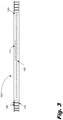
- Fig. 3 is diagram of a MEMS die (160) illustrating one example of the principles described herein.
- the MEMS die (160) includes a number of components including an opening (180), a number of jets (170), and a pad (330) that provides for a plurality of electrical connections (340).
- the electrical connections (340) facilitate communication between the components of the MEMS die (160) and the PHA ASIC (150).
- a MEMS die (160) includes a thermal sensor (390).
- a MEMS die (160) includes a heater. In some examples, heating is provided using a number of resistors located within each of a number of firing chambers of the MEMS die (160).
- the thermal sensor (390) is controlled by the PHA ASIC (150). In another example, the thermal sensor (390) is controlled on the MEMS die (160). In some examples, the jets (170) form a column along the opening (180). In other examples, the jets (170) form columns on both sides of the opening (180).
- the MEMS die (160) may have a single pad (330) on one end of the MEMS die (160). In another example, the MEMS die (160) has pads (330) on both ends of the MEMS die (160). In still another example, the MEMS die (160) has a pad (330) located on the side and/or in the body of the MEMS die (160) to facilitate additional connections.
- Silicon wafers are produced from silicon ingots, which tend to be of limited dimensions; often six or eight inches in diameter. Larger ingots and larger wafers are more expensive on a per area basis than smaller ingots and wafers, due in part to the increasing difficulty of producing larger, high purity silicon. Further, because few large dice may fit on a wafer, the cost for them is accordingly higher than for smaller dice that may make more efficient use of the area of the wafer. As a result, the cost of devices built on silicon substrates increase faster than the area of the devices, with larger MEMS die (160) costing disproportionately more than smaller MEMS die (160).
- the defect rate in a MEMS die (160) or integrated circuit device is dependent upon the complexity of the device.
- the same argument used with respect to the single opening assembly applies to other components of the MEMS. Accordingly, all other factors being equal, a simpler device is more likely to have better yields from a semiconductor or MEMS fabrication process. Accordingly, designs that may reduce the number of elements may increase yield.
- just moving the complexity from one part of design to another part of the design may not produce overall yield gains.
- moving complexity from high cost components to lower cost components may produce savings.
- moving complexity from a component made by a process with a higher defect rate to a component made by a process with a lower defect rate may produce significant yield and cost savings.
- the MEMS dice (160) are interchangeable.
- the advantages of using a standardized design include: reduced number of parts, simpler assembly (less need to complicate the connections with different types of connections), increase manufacturing efficiencies, fewer part numbers, and lower inventory quantities and costs.
- the MEMS die (160) used in a printhead include more than one design.
- the black ink die may have a higher or lower nozzle density than the color ink die or the color ink die may be a three opening die while the black ink die is a single opening die.
- the high utilization portion of a page width printhead (140) along the left margin may have a different design to accommodate the different usage rate.
- the MEMS die (160) are modular such that they may be placed in the same location but include different functionalities allowing multiple configurations of the printhead (140) to be built using some common components.
- the printer ASIC (520) provides the original or a modified form of the image data (510) to the printhead assembly application specific integrated circuit (PHA ASIC) (150). This may be accomplished using a communications link (230).
- the communications link (230) may be optical, electrical, electromagnetic, or any suitable device and associated communications technologies used in data transfer.
- the communications link (230) is a wireless local area network (WLAN) signal such as a Wi-Fi signal standard developed by the Wi-Fi Alliance, communication technologies developed by the BLUETOOTH® Special Interest Group, infrared signals, Radio Frequency signal, low-voltage differential signaling (LVDS), transition-minimized differential signaling (TMDS), reduced swing differential signaling (RSDS), bus low voltage differential signaling (BLVDS), differential stub series terminated logic (SSTL), differential high speed transceiver logic (HSTL) and/or similar communications technologies and their respective communications devices.
- the communications link (230) includes a low-voltage differential signaling (LVDS) pair cable.
- the communications link (230) is a plurality of high speed data lines.
- the communication link (230) includes a discrete clock signal.
- the communication link (230) has an embedded clock signal that is extracted by the PHA ASIC (150).
- the error correction performed by the error correction circuit (540) may include the inclusion of a parity bit or sum bit periodically in the communication link (230) between the printer ASIC (520) and PHA ASIC (150).
- the error correction circuit (540) may include more sophisticated error correction methodologies including those error correction methodologies associated with controlling and verifying data compression and decompression.
- the PHA ASIC (150) may further process the image data (510).
- the firing patterns to produce the image are created by the PHA ASIC (150).
- the firing patterns used to produce the image are created by the printer ASIC (520).
- the firing pattern is provided as part of the image data (510) or the image data (510) may be sent in a ready to print format.
- the PHA ASIC (150) may separate the image data (510) into signals provided to the individual MEMS die (160). These signals may be provided to the MEMS die (160) using the transmission lines (270). Because of the large numbers of jets (170) on a MEMS die (160), the data may be provided serially over the transmission lines (270).
- This bubble expands, causing a droplet of ink to be expelled from the nozzle of the jet (170) toward the printing medium.
- the bubble then collapses, allowing more fluid into the jet (170) to prepare it for them next firing.
- the fluid may be ink, toner or some other marking fluid.
- Fig. 6 shows a flowchart for a process of printing (600) according to the principles described herein. This includes the processes of receiving (block 610) data to a printhead assembly (PHA) application specific integrated circuit (ASIC) (150); processing (block 620) the data into a plurality of data signals; transmitting (block 630) the data signals through a shared substrate (210) from the PHA ASIC (150) to a plurality of microelectromechanical systems (MEMS) dice (160); and firing (block 640) a plurality of ink jets (170) located on the MEMS dice (160).
- PHA printhead assembly
- ASIC application specific integrated circuit
- MEMS microelectromechanical systems
- the fire control signal may be directed at just those jets (170) that should fire.
- a fire/don't fire signal is loaded into an storage element, between the fire control line (280) and the jet (170) such that only those jets (170) with a fire signal loaded into the storage element receive the fire control signal.
- a suppression signal is provided to jets (170) that should not fire, which inactivates those jets (170).
Landscapes
- Particle Formation And Scattering Control In Inkjet Printers (AREA)
- Micromachines (AREA)
Claims (15)
- Druckkopfanordnung, PHA (140), die Folgendes umfasst:mehrere modulare Mikroelektromechanisches-System-Chips, MEMS-Chips (160), die auf einem Substrat (210) angebracht sind, wobei jeder MEMS-Chip (160) Folgendes umfasst:eine Öffnung (180), die in dem Chip (160) definiert ist,mehrere Düsen (170), die der Öffnung (180) in Fluidverbindung mit der Öffnung benachbart sind, undein Pad (330), um elektrische Steuersignale zu empfangen; undmehrere Übertragungsleitungen (270), die elektrische Signale an den MEMS-Chip (160) übertragen; dadurch gekennzeichnet, dassdie Druckkopfanordnung (140) ferner einen vereinheitlichten eingebauten Controller in der Form eines anwendungsspezifischen integrierten Schaltkreises, ASIC (150) umfasst, der getrennt von dem MEMS-Chip (160) auf dem Substrat (210) angebracht und mit den mehreren Übertragungsleitungen (270) verbunden ist.
- Druckkopfanordnung (140) nach Anspruch 1, die ferner Folgendes umfasst:
eine Kommunikationsverbindung (230), um wenigstens ein Signal von außerhalb der Druckkopfanordnung zu empfangen. - Druckkopfanordnung (140) nach Anspruch 1, die ferner eine Polymerbeschichtung umfasst.
- Druckkopfanordnung (140) nach Anspruch 1, wobei jeder MEMS-Chip (160) ferner Folgendes umfasst:einen in den MEMS-Chip (160) integrierten Wärmesensor (390),wobei die Messschaltung für den Wärmesensor (390) von dem ASIC (150) bereitgestellt wird.
- Druckkopfanordnung (140) nach Anspruch 2, wobei der ASIC (150) eine Fehlerkorrekturschaltung zum Durchführen einer Fehlerkorrektur an dem über die Kommunikationsverbindung (230) empfangenen Signal beinhaltet.
- Druckkopfanordnung (140) nach Anspruch 2, wobei die Kommunikationsverbindung (230) eine drahtlose Verbindung ist.
- Druckkopfanordnung (140) nach Anspruch 2, wobei der ASIC (150) angeordnet ist, um über die Kommunikationsverbindung (230) mit einem Drucker-ASIC (520) verbunden zu werden, und das über die Kommunikationsverbindung (230) empfangene Signal Daten eines Druckauftrags, der von dem Drucker-ASIC (520) gesendet wurde, umfasst.
- Druckkopfanordnung (140) nach Anspruch 2, wobei die Kommunikationsverbindung (230) angeordnet ist, um ein diskretes oder eingebettetes Taktsignal in dem Signal zu beinhalten, und der ASIC (150) angeordnet ist, um einen Takt aus einem über die Kommunikationsverbindung (230) empfangenen Signal zu extrahieren.
- Druckkopfanordnung (140) nach Anspruch 1, wobei zwei oder mehr der MEMS-Chips (160) äquivalent sind.
- Druckkopfanordnung (140) nach Anspruch 8, wobei die Übertragungsleitungen (270) derart angeordnet sind, dass ein MEMS-Chip (160) Signale von einem anderen MEMS-Chip (160) der Druckkopfanordnung (140) empfängt.
- Druckkopfanordnung nach Anspruch 8, wobei der MEMS-Chip (160) einen Herstellungsvorgang aufweist, der sich von einem Herstellungsvorgang des ASIC (150) unterscheidet, wobei jeder Herstellungsvorgang eine minimale Merkmalsgröße aufweist, wobei die minimale Merkmalsgröße auf jedem MEMS-Chip (160) größer als die minimale Merkmalsgröße des ASIC (150) ist.
- Verfahren zum Drucken anhand einer Druckkopfanordnung (140), das Folgendes umfasst:Empfangen von Daten durch einen vereinheitlichen eingebauten Controller der Druckkopfanordnung (140) in der Form einer Druckkopfanordnung, PHA, einer anwendungsspezifischen integrierten Schaltung (ASIC) (150);Verarbeiten der Daten zu mehreren Datensignalen;Übertragen der Datensignale über ein gemeinsames Substrat (210) von dem PHA-ASIC (150) zu mehreren Mikroelektromechanisches-System-Chips, MEMS-Chips (160) der Druckkopfanordnung (140), wobei der MEMS-Chip (160) von dem ASIC (150) getrennt ist; undAbfeuern mehrerer Tintenstrahlen (170), die sich auf dem MEMS-Chip (160) befinden, als Reaktion auf die Datensignale.
- Verfahren nach Anspruch 12, wobei die mehreren Datensignale ein Taktsignal beinhalten.
- Verfahren nach Anspruch 12, wobei das Übertragen umfasst, dass der ASIC (150) den Zeitpunkt des Abfeuerns der Tintenstrahlen (170) verteilt, um den Spitzenbedarf an Leistung in einem MEMS-Chip (160) zu begrenzen.
- Verfahren nach Anspruch 12, wobei die elektrischen Steuersignale Abfeuersteuersignale beinhalten und das Übertragen umfasst, dass der ASIC (150) die Abfeuersteuersignale verteilt, um den Spitzenbedarf an Leistung zu begrenzen.
Applications Claiming Priority (1)
| Application Number | Priority Date | Filing Date | Title |
|---|---|---|---|
| PCT/US2014/062667 WO2016068884A1 (en) | 2014-10-28 | 2014-10-28 | Printhead with microelectromechanical die and application specific integrated circuit |
Publications (3)
| Publication Number | Publication Date |
|---|---|
| EP3212411A1 EP3212411A1 (de) | 2017-09-06 |
| EP3212411A4 EP3212411A4 (de) | 2018-06-13 |
| EP3212411B1 true EP3212411B1 (de) | 2019-11-27 |
Family
ID=55857999
Family Applications (1)
| Application Number | Title | Priority Date | Filing Date |
|---|---|---|---|
| EP14904744.1A Active EP3212411B1 (de) | 2014-10-28 | 2014-10-28 | Druckkopf mit mikroelektromechanischer matrize und anwendungsspezifische integrierte schaltung |
Country Status (4)
| Country | Link |
|---|---|
| US (3) | US10189248B2 (de) |
| EP (1) | EP3212411B1 (de) |
| CN (1) | CN107073954B (de) |
| WO (1) | WO2016068884A1 (de) |
Families Citing this family (6)
| Publication number | Priority date | Publication date | Assignee | Title |
|---|---|---|---|---|
| EP3212412B1 (de) * | 2014-10-28 | 2021-02-17 | Hewlett-Packard Development Company, L.P. | Breites gruppendruckkopfmodul |
| EP3212411B1 (de) * | 2014-10-28 | 2019-11-27 | Hewlett-Packard Development Company, L.P. | Druckkopf mit mikroelektromechanischer matrize und anwendungsspezifische integrierte schaltung |
| US11260653B2 (en) | 2017-01-20 | 2022-03-01 | Hewlett-Packard Development Company, L.P. | Configuring communication interfaces of fluid ejection devices |
| EP3600897A4 (de) | 2017-07-12 | 2020-11-11 | Hewlett-Packard Development Company, L.P. | Fluidische matrize |
| JP7027209B2 (ja) * | 2018-03-23 | 2022-03-01 | 富士通コンポーネント株式会社 | 記録紙カセット及び印刷システム |
| JP7593192B2 (ja) * | 2021-03-26 | 2024-12-03 | セイコーエプソン株式会社 | 液体吐出装置 |
Family Cites Families (19)
| Publication number | Priority date | Publication date | Assignee | Title |
|---|---|---|---|---|
| US6357863B1 (en) | 1999-12-02 | 2002-03-19 | Lexmark International Inc. | Linear substrate heater for ink jet print head chip |
| US7133153B2 (en) | 2000-08-31 | 2006-11-07 | Canon Kabushiki Kaisha | Printhead having digital circuit and analog circuit, and printing apparatus using the same |
| DE60204485T2 (de) | 2001-01-05 | 2006-03-16 | Hewlett-Packard Development Co., L.P., Houston | Integrierter programmierbarer Auslösepulsgenerator für Tintenstrahldruckkopf |
| US6543883B1 (en) | 2001-09-29 | 2003-04-08 | Hewlett-Packard Company | Fluid ejection device with drive circuitry proximate to heating element |
| JP4374834B2 (ja) * | 2002-08-12 | 2009-12-02 | セイコーエプソン株式会社 | カートリッジおよび記録装置 |
| US7096137B2 (en) | 2002-12-02 | 2006-08-22 | Silverbrook Research Pty Ltd | Clock trim mechanism for onboard system clock |
| US7549718B2 (en) | 2004-05-27 | 2009-06-23 | Silverbrook Research Pty Ltd | Printhead module having operation controllable on basis of thermal sensors |
| JP4194580B2 (ja) | 2004-06-02 | 2008-12-10 | キヤノン株式会社 | ヘッド基板、記録ヘッド、ヘッドカートリッジ、及び記録装置 |
| WO2011005699A2 (en) * | 2009-07-10 | 2011-01-13 | Fujifilm Dimatix, Inc. | Mems jetting structure for dense packing |
| US8425004B2 (en) * | 2009-07-24 | 2013-04-23 | Zamtec Ltd | Printhead having polymer incorporating nanoparticles coated on ink ejection face |
| US8342652B2 (en) | 2010-05-27 | 2013-01-01 | Xerox Corporation | Molded nozzle plate with alignment features for simplified assembly |
| US9044942B2 (en) | 2010-09-30 | 2015-06-02 | Hewlett-Packard Development Company, L.P. | Thermal sensing fluid ejection assembly and method |
| US20120212780A1 (en) * | 2011-02-21 | 2012-08-23 | Canon Kabushiki Kaisha | Printing apparatus and electronic device |
| BR112013031747A2 (pt) * | 2011-06-29 | 2016-12-13 | Hewlett Packard Development Co | leiaute de traços de cabeçote de impressão piezelétrico |
| US8690296B2 (en) | 2012-01-27 | 2014-04-08 | Eastman Kodak Company | Inkjet printhead with multi-layer mounting substrate |
| US8608283B1 (en) * | 2012-06-27 | 2013-12-17 | Eastman Kodak Company | Nozzle array configuration for printhead die |
| KR101964494B1 (ko) | 2012-11-30 | 2019-04-01 | 휴렛-팩커드 디벨롭먼트 컴퍼니, 엘.피. | 집적형 잉크 레벨 센서를 구비한 유체 분출 디바이스 |
| GB2530047B (en) * | 2014-09-10 | 2017-05-03 | Xaar Technology Ltd | Printhead circuit with trimming |
| EP3212411B1 (de) * | 2014-10-28 | 2019-11-27 | Hewlett-Packard Development Company, L.P. | Druckkopf mit mikroelektromechanischer matrize und anwendungsspezifische integrierte schaltung |
-
2014
- 2014-10-28 EP EP14904744.1A patent/EP3212411B1/de active Active
- 2014-10-28 US US15/518,299 patent/US10189248B2/en active Active
- 2014-10-28 WO PCT/US2014/062667 patent/WO2016068884A1/en not_active Ceased
- 2014-10-28 CN CN201480083114.5A patent/CN107073954B/zh active Active
-
2019
- 2019-01-04 US US16/240,562 patent/US10434768B2/en active Active
- 2019-08-27 US US16/552,447 patent/US10836159B2/en active Active
Non-Patent Citations (1)
| Title |
|---|
| None * |
Also Published As
| Publication number | Publication date |
|---|---|
| CN107073954A (zh) | 2017-08-18 |
| EP3212411A1 (de) | 2017-09-06 |
| CN107073954B (zh) | 2020-04-17 |
| US20170313058A1 (en) | 2017-11-02 |
| WO2016068884A1 (en) | 2016-05-06 |
| US10836159B2 (en) | 2020-11-17 |
| US20190152221A1 (en) | 2019-05-23 |
| US20190381789A1 (en) | 2019-12-19 |
| EP3212411A4 (de) | 2018-06-13 |
| US10189248B2 (en) | 2019-01-29 |
| US10434768B2 (en) | 2019-10-08 |
Similar Documents
| Publication | Publication Date | Title |
|---|---|---|
| US10836159B2 (en) | Apparatus with microelectromechanical die and application specific integrated circuit | |
| EP3212405B1 (de) | Druckkopfausstosssignalsteuerung | |
| CN101985254B (zh) | 流体喷射装置和流体喷射方法 | |
| US8622499B2 (en) | Liquid ejection apparatus and ejection control method for same, and inkjet apparatus | |
| CN107073939B (zh) | 打印头和喷墨打印机 | |
| JP6043556B2 (ja) | インクジェット印刷装置 | |
| US9950520B2 (en) | Printhead having a number of single-dimensional memristor banks | |
| JP2018016054A (ja) | 素子基板、記録ヘッド、及び記録装置 | |
| JP2022060431A (ja) | 液体吐出ヘッド及び液体吐出装置 | |
| EP3717247B1 (de) | Druckkomponente mit speichermatrix mit intermittierendem taktsignal | |
| AU2013406231B2 (en) | Fluid ejection apparatus with single power supply connector | |
| CN103057270B (zh) | 流体喷射装置和流体喷射方法 | |
| JP2012139980A (ja) | インク吐出装置、画像記録装置、インク吐出方法、及びプログラム | |
| JP2006181760A (ja) | 記録ヘッド用素子基板、記録ヘッドおよび記録装置 | |
| CN109318595A (zh) | 打印头及喷墨式打印方法 | |
| CN102985259B (zh) | 多模式打印 | |
| JP4730655B2 (ja) | 液体吐出装置 | |
| JP6300551B2 (ja) | 液体吐出装置および液体吐出方法 | |
| JP2013193280A (ja) | 記録装置 | |
| JP2016002711A (ja) | インク吐出装置、制御装置およびインク吐出制御方法 | |
| HK40038647A (en) | Print component with memory array using intermittent clock signal | |
| HK40038647B (en) | Print component with memory array using intermittent clock signal | |
| HK1229768A1 (en) | Fluid ejection apparatus with single power supply connector |
Legal Events
| Date | Code | Title | Description |
|---|---|---|---|
| STAA | Information on the status of an ep patent application or granted ep patent |
Free format text: STATUS: THE INTERNATIONAL PUBLICATION HAS BEEN MADE |
|
| PUAI | Public reference made under article 153(3) epc to a published international application that has entered the european phase |
Free format text: ORIGINAL CODE: 0009012 |
|
| STAA | Information on the status of an ep patent application or granted ep patent |
Free format text: STATUS: REQUEST FOR EXAMINATION WAS MADE |
|
| 17P | Request for examination filed |
Effective date: 20170407 |
|
| AK | Designated contracting states |
Kind code of ref document: A1 Designated state(s): AL AT BE BG CH CY CZ DE DK EE ES FI FR GB GR HR HU IE IS IT LI LT LU LV MC MK MT NL NO PL PT RO RS SE SI SK SM TR |
|
| AX | Request for extension of the european patent |
Extension state: BA ME |
|
| DAX | Request for extension of the european patent (deleted) | ||
| A4 | Supplementary search report drawn up and despatched |
Effective date: 20180516 |
|
| RIC1 | Information provided on ipc code assigned before grant |
Ipc: B41J 2/045 20060101ALI20180509BHEP Ipc: B41J 2/175 20060101AFI20180509BHEP Ipc: B41J 2/14 20060101ALI20180509BHEP Ipc: B41J 29/393 20060101ALI20180509BHEP |
|
| RAP1 | Party data changed (applicant data changed or rights of an application transferred) |
Owner name: HEWLETT-PACKARD DEVELOPMENT COMPANY, L.P. |
|
| GRAP | Despatch of communication of intention to grant a patent |
Free format text: ORIGINAL CODE: EPIDOSNIGR1 |
|
| STAA | Information on the status of an ep patent application or granted ep patent |
Free format text: STATUS: GRANT OF PATENT IS INTENDED |
|
| INTG | Intention to grant announced |
Effective date: 20190621 |
|
| GRAS | Grant fee paid |
Free format text: ORIGINAL CODE: EPIDOSNIGR3 |
|
| GRAA | (expected) grant |
Free format text: ORIGINAL CODE: 0009210 |
|
| STAA | Information on the status of an ep patent application or granted ep patent |
Free format text: STATUS: THE PATENT HAS BEEN GRANTED |
|
| AK | Designated contracting states |
Kind code of ref document: B1 Designated state(s): AL AT BE BG CH CY CZ DE DK EE ES FI FR GB GR HR HU IE IS IT LI LT LU LV MC MK MT NL NO PL PT RO RS SE SI SK SM TR |
|
| REG | Reference to a national code |
Ref country code: GB Ref legal event code: FG4D |
|
| REG | Reference to a national code |
Ref country code: CH Ref legal event code: EP |
|
| REG | Reference to a national code |
Ref country code: AT Ref legal event code: REF Ref document number: 1206222 Country of ref document: AT Kind code of ref document: T Effective date: 20191215 |
|
| REG | Reference to a national code |
Ref country code: DE Ref legal event code: R096 Ref document number: 602014057668 Country of ref document: DE |
|
| REG | Reference to a national code |
Ref country code: IE Ref legal event code: FG4D |
|
| REG | Reference to a national code |
Ref country code: NL Ref legal event code: MP Effective date: 20191127 |
|
| REG | Reference to a national code |
Ref country code: LT Ref legal event code: MG4D |
|
| PG25 | Lapsed in a contracting state [announced via postgrant information from national office to epo] |
Ref country code: SE Free format text: LAPSE BECAUSE OF FAILURE TO SUBMIT A TRANSLATION OF THE DESCRIPTION OR TO PAY THE FEE WITHIN THE PRESCRIBED TIME-LIMIT Effective date: 20191127 Ref country code: LV Free format text: LAPSE BECAUSE OF FAILURE TO SUBMIT A TRANSLATION OF THE DESCRIPTION OR TO PAY THE FEE WITHIN THE PRESCRIBED TIME-LIMIT Effective date: 20191127 Ref country code: NL Free format text: LAPSE BECAUSE OF FAILURE TO SUBMIT A TRANSLATION OF THE DESCRIPTION OR TO PAY THE FEE WITHIN THE PRESCRIBED TIME-LIMIT Effective date: 20191127 Ref country code: FI Free format text: LAPSE BECAUSE OF FAILURE TO SUBMIT A TRANSLATION OF THE DESCRIPTION OR TO PAY THE FEE WITHIN THE PRESCRIBED TIME-LIMIT Effective date: 20191127 Ref country code: BG Free format text: LAPSE BECAUSE OF FAILURE TO SUBMIT A TRANSLATION OF THE DESCRIPTION OR TO PAY THE FEE WITHIN THE PRESCRIBED TIME-LIMIT Effective date: 20200227 Ref country code: LT Free format text: LAPSE BECAUSE OF FAILURE TO SUBMIT A TRANSLATION OF THE DESCRIPTION OR TO PAY THE FEE WITHIN THE PRESCRIBED TIME-LIMIT Effective date: 20191127 Ref country code: NO Free format text: LAPSE BECAUSE OF FAILURE TO SUBMIT A TRANSLATION OF THE DESCRIPTION OR TO PAY THE FEE WITHIN THE PRESCRIBED TIME-LIMIT Effective date: 20200227 Ref country code: GR Free format text: LAPSE BECAUSE OF FAILURE TO SUBMIT A TRANSLATION OF THE DESCRIPTION OR TO PAY THE FEE WITHIN THE PRESCRIBED TIME-LIMIT Effective date: 20200228 |
|
| PG25 | Lapsed in a contracting state [announced via postgrant information from national office to epo] |
Ref country code: RS Free format text: LAPSE BECAUSE OF FAILURE TO SUBMIT A TRANSLATION OF THE DESCRIPTION OR TO PAY THE FEE WITHIN THE PRESCRIBED TIME-LIMIT Effective date: 20191127 Ref country code: HR Free format text: LAPSE BECAUSE OF FAILURE TO SUBMIT A TRANSLATION OF THE DESCRIPTION OR TO PAY THE FEE WITHIN THE PRESCRIBED TIME-LIMIT Effective date: 20191127 Ref country code: IS Free format text: LAPSE BECAUSE OF FAILURE TO SUBMIT A TRANSLATION OF THE DESCRIPTION OR TO PAY THE FEE WITHIN THE PRESCRIBED TIME-LIMIT Effective date: 20200327 |
|
| PG25 | Lapsed in a contracting state [announced via postgrant information from national office to epo] |
Ref country code: AL Free format text: LAPSE BECAUSE OF FAILURE TO SUBMIT A TRANSLATION OF THE DESCRIPTION OR TO PAY THE FEE WITHIN THE PRESCRIBED TIME-LIMIT Effective date: 20191127 |
|
| PG25 | Lapsed in a contracting state [announced via postgrant information from national office to epo] |
Ref country code: RO Free format text: LAPSE BECAUSE OF FAILURE TO SUBMIT A TRANSLATION OF THE DESCRIPTION OR TO PAY THE FEE WITHIN THE PRESCRIBED TIME-LIMIT Effective date: 20191127 Ref country code: CZ Free format text: LAPSE BECAUSE OF FAILURE TO SUBMIT A TRANSLATION OF THE DESCRIPTION OR TO PAY THE FEE WITHIN THE PRESCRIBED TIME-LIMIT Effective date: 20191127 Ref country code: ES Free format text: LAPSE BECAUSE OF FAILURE TO SUBMIT A TRANSLATION OF THE DESCRIPTION OR TO PAY THE FEE WITHIN THE PRESCRIBED TIME-LIMIT Effective date: 20191127 Ref country code: EE Free format text: LAPSE BECAUSE OF FAILURE TO SUBMIT A TRANSLATION OF THE DESCRIPTION OR TO PAY THE FEE WITHIN THE PRESCRIBED TIME-LIMIT Effective date: 20191127 Ref country code: PT Free format text: LAPSE BECAUSE OF FAILURE TO SUBMIT A TRANSLATION OF THE DESCRIPTION OR TO PAY THE FEE WITHIN THE PRESCRIBED TIME-LIMIT Effective date: 20200419 Ref country code: DK Free format text: LAPSE BECAUSE OF FAILURE TO SUBMIT A TRANSLATION OF THE DESCRIPTION OR TO PAY THE FEE WITHIN THE PRESCRIBED TIME-LIMIT Effective date: 20191127 |
|
| REG | Reference to a national code |
Ref country code: DE Ref legal event code: R097 Ref document number: 602014057668 Country of ref document: DE |
|
| PG25 | Lapsed in a contracting state [announced via postgrant information from national office to epo] |
Ref country code: SK Free format text: LAPSE BECAUSE OF FAILURE TO SUBMIT A TRANSLATION OF THE DESCRIPTION OR TO PAY THE FEE WITHIN THE PRESCRIBED TIME-LIMIT Effective date: 20191127 Ref country code: SM Free format text: LAPSE BECAUSE OF FAILURE TO SUBMIT A TRANSLATION OF THE DESCRIPTION OR TO PAY THE FEE WITHIN THE PRESCRIBED TIME-LIMIT Effective date: 20191127 |
|
| REG | Reference to a national code |
Ref country code: AT Ref legal event code: MK05 Ref document number: 1206222 Country of ref document: AT Kind code of ref document: T Effective date: 20191127 |
|
| PLBE | No opposition filed within time limit |
Free format text: ORIGINAL CODE: 0009261 |
|
| STAA | Information on the status of an ep patent application or granted ep patent |
Free format text: STATUS: NO OPPOSITION FILED WITHIN TIME LIMIT |
|
| 26N | No opposition filed |
Effective date: 20200828 |
|
| PG25 | Lapsed in a contracting state [announced via postgrant information from national office to epo] |
Ref country code: SI Free format text: LAPSE BECAUSE OF FAILURE TO SUBMIT A TRANSLATION OF THE DESCRIPTION OR TO PAY THE FEE WITHIN THE PRESCRIBED TIME-LIMIT Effective date: 20191127 Ref country code: AT Free format text: LAPSE BECAUSE OF FAILURE TO SUBMIT A TRANSLATION OF THE DESCRIPTION OR TO PAY THE FEE WITHIN THE PRESCRIBED TIME-LIMIT Effective date: 20191127 Ref country code: PL Free format text: LAPSE BECAUSE OF FAILURE TO SUBMIT A TRANSLATION OF THE DESCRIPTION OR TO PAY THE FEE WITHIN THE PRESCRIBED TIME-LIMIT Effective date: 20191127 |
|
| PG25 | Lapsed in a contracting state [announced via postgrant information from national office to epo] |
Ref country code: IT Free format text: LAPSE BECAUSE OF FAILURE TO SUBMIT A TRANSLATION OF THE DESCRIPTION OR TO PAY THE FEE WITHIN THE PRESCRIBED TIME-LIMIT Effective date: 20191127 |
|
| REG | Reference to a national code |
Ref country code: CH Ref legal event code: PL |
|
| PG25 | Lapsed in a contracting state [announced via postgrant information from national office to epo] |
Ref country code: LU Free format text: LAPSE BECAUSE OF NON-PAYMENT OF DUE FEES Effective date: 20201028 Ref country code: MC Free format text: LAPSE BECAUSE OF FAILURE TO SUBMIT A TRANSLATION OF THE DESCRIPTION OR TO PAY THE FEE WITHIN THE PRESCRIBED TIME-LIMIT Effective date: 20191127 |
|
| REG | Reference to a national code |
Ref country code: BE Ref legal event code: MM Effective date: 20201031 |
|
| PG25 | Lapsed in a contracting state [announced via postgrant information from national office to epo] |
Ref country code: CH Free format text: LAPSE BECAUSE OF NON-PAYMENT OF DUE FEES Effective date: 20201031 Ref country code: BE Free format text: LAPSE BECAUSE OF NON-PAYMENT OF DUE FEES Effective date: 20201031 Ref country code: LI Free format text: LAPSE BECAUSE OF NON-PAYMENT OF DUE FEES Effective date: 20201031 |
|
| PG25 | Lapsed in a contracting state [announced via postgrant information from national office to epo] |
Ref country code: IE Free format text: LAPSE BECAUSE OF NON-PAYMENT OF DUE FEES Effective date: 20201028 |
|
| PG25 | Lapsed in a contracting state [announced via postgrant information from national office to epo] |
Ref country code: TR Free format text: LAPSE BECAUSE OF FAILURE TO SUBMIT A TRANSLATION OF THE DESCRIPTION OR TO PAY THE FEE WITHIN THE PRESCRIBED TIME-LIMIT Effective date: 20191127 Ref country code: MT Free format text: LAPSE BECAUSE OF FAILURE TO SUBMIT A TRANSLATION OF THE DESCRIPTION OR TO PAY THE FEE WITHIN THE PRESCRIBED TIME-LIMIT Effective date: 20191127 Ref country code: CY Free format text: LAPSE BECAUSE OF FAILURE TO SUBMIT A TRANSLATION OF THE DESCRIPTION OR TO PAY THE FEE WITHIN THE PRESCRIBED TIME-LIMIT Effective date: 20191127 |
|
| PG25 | Lapsed in a contracting state [announced via postgrant information from national office to epo] |
Ref country code: MK Free format text: LAPSE BECAUSE OF FAILURE TO SUBMIT A TRANSLATION OF THE DESCRIPTION OR TO PAY THE FEE WITHIN THE PRESCRIBED TIME-LIMIT Effective date: 20191127 |
|
| PGFP | Annual fee paid to national office [announced via postgrant information from national office to epo] |
Ref country code: GB Payment date: 20230920 Year of fee payment: 10 |
|
| PGFP | Annual fee paid to national office [announced via postgrant information from national office to epo] |
Ref country code: FR Payment date: 20230920 Year of fee payment: 10 |
|
| GBPC | Gb: european patent ceased through non-payment of renewal fee |
Effective date: 20241028 |
|
| PG25 | Lapsed in a contracting state [announced via postgrant information from national office to epo] |
Ref country code: GB Free format text: LAPSE BECAUSE OF NON-PAYMENT OF DUE FEES Effective date: 20241028 |
|
| PG25 | Lapsed in a contracting state [announced via postgrant information from national office to epo] |
Ref country code: FR Free format text: LAPSE BECAUSE OF NON-PAYMENT OF DUE FEES Effective date: 20241031 |
|
| REG | Reference to a national code |
Ref country code: DE Ref legal event code: R082 Ref document number: 602014057668 Country of ref document: DE Representative=s name: NOVAGRAAF BREVETS, FR |
|
| PGFP | Annual fee paid to national office [announced via postgrant information from national office to epo] |
Ref country code: DE Payment date: 20250923 Year of fee payment: 12 |