EP3213374B1 - Connecteur d'alimentation - Google Patents
Connecteur d'alimentation Download PDFInfo
- Publication number
- EP3213374B1 EP3213374B1 EP15790778.3A EP15790778A EP3213374B1 EP 3213374 B1 EP3213374 B1 EP 3213374B1 EP 15790778 A EP15790778 A EP 15790778A EP 3213374 B1 EP3213374 B1 EP 3213374B1
- Authority
- EP
- European Patent Office
- Prior art keywords
- contact
- base
- connector
- power connector
- terminals
- Prior art date
- Legal status (The legal status is an assumption and is not a legal conclusion. Google has not performed a legal analysis and makes no representation as to the accuracy of the status listed.)
- Active
Links
Images


Classifications
-
- H—ELECTRICITY
- H01—ELECTRIC ELEMENTS
- H01R—ELECTRICALLY-CONDUCTIVE CONNECTIONS; STRUCTURAL ASSOCIATIONS OF A PLURALITY OF MUTUALLY-INSULATED ELECTRICAL CONNECTING ELEMENTS; COUPLING DEVICES; CURRENT COLLECTORS
- H01R24/00—Two-part coupling devices, or either of their cooperating parts, characterised by their overall structure
- H01R24/76—Two-part coupling devices, or either of their cooperating parts, characterised by their overall structure with sockets, clips or analogous contacts and secured to apparatus or structure, e.g. to a wall
-
- H—ELECTRICITY
- H01—ELECTRIC ELEMENTS
- H01R—ELECTRICALLY-CONDUCTIVE CONNECTIONS; STRUCTURAL ASSOCIATIONS OF A PLURALITY OF MUTUALLY-INSULATED ELECTRICAL CONNECTING ELEMENTS; COUPLING DEVICES; CURRENT COLLECTORS
- H01R13/00—Details of coupling devices of the kinds covered by groups H01R12/70 or H01R24/00 - H01R33/00
- H01R13/02—Contact members
- H01R13/10—Sockets for co-operation with pins or blades
- H01R13/11—Resilient sockets
- H01R13/111—Resilient sockets co-operating with pins having a circular transverse section
-
- H—ELECTRICITY
- H01—ELECTRIC ELEMENTS
- H01R—ELECTRICALLY-CONDUCTIVE CONNECTIONS; STRUCTURAL ASSOCIATIONS OF A PLURALITY OF MUTUALLY-INSULATED ELECTRICAL CONNECTING ELEMENTS; COUPLING DEVICES; CURRENT COLLECTORS
- H01R12/00—Structural associations of a plurality of mutually-insulated electrical connecting elements, specially adapted for printed circuits, e.g. printed circuit boards [PCB], flat or ribbon cables, or like generally planar structures, e.g. terminal strips, terminal blocks; Coupling devices specially adapted for printed circuits, flat or ribbon cables, or like generally planar structures; Terminals specially adapted for contact with, or insertion into, printed circuits, flat or ribbon cables, or like generally planar structures
- H01R12/50—Fixed connections
- H01R12/51—Fixed connections for rigid printed circuits or like structures
- H01R12/55—Fixed connections for rigid printed circuits or like structures characterised by the terminals
-
- H—ELECTRICITY
- H01—ELECTRIC ELEMENTS
- H01R—ELECTRICALLY-CONDUCTIVE CONNECTIONS; STRUCTURAL ASSOCIATIONS OF A PLURALITY OF MUTUALLY-INSULATED ELECTRICAL CONNECTING ELEMENTS; COUPLING DEVICES; CURRENT COLLECTORS
- H01R12/00—Structural associations of a plurality of mutually-insulated electrical connecting elements, specially adapted for printed circuits, e.g. printed circuit boards [PCB], flat or ribbon cables, or like generally planar structures, e.g. terminal strips, terminal blocks; Coupling devices specially adapted for printed circuits, flat or ribbon cables, or like generally planar structures; Terminals specially adapted for contact with, or insertion into, printed circuits, flat or ribbon cables, or like generally planar structures
- H01R12/70—Coupling devices
- H01R12/71—Coupling devices for rigid printing circuits or like structures
- H01R12/712—Coupling devices for rigid printing circuits or like structures co-operating with the surface of the printed circuit or with a coupling device exclusively provided on the surface of the printed circuit
- H01R12/716—Coupling device provided on the PCB
-
- H—ELECTRICITY
- H01—ELECTRIC ELEMENTS
- H01R—ELECTRICALLY-CONDUCTIVE CONNECTIONS; STRUCTURAL ASSOCIATIONS OF A PLURALITY OF MUTUALLY-INSULATED ELECTRICAL CONNECTING ELEMENTS; COUPLING DEVICES; CURRENT COLLECTORS
- H01R12/00—Structural associations of a plurality of mutually-insulated electrical connecting elements, specially adapted for printed circuits, e.g. printed circuit boards [PCB], flat or ribbon cables, or like generally planar structures, e.g. terminal strips, terminal blocks; Coupling devices specially adapted for printed circuits, flat or ribbon cables, or like generally planar structures; Terminals specially adapted for contact with, or insertion into, printed circuits, flat or ribbon cables, or like generally planar structures
- H01R12/70—Coupling devices
- H01R12/71—Coupling devices for rigid printing circuits or like structures
- H01R12/72—Coupling devices for rigid printing circuits or like structures coupling with the edge of the rigid printed circuits or like structures
- H01R12/721—Coupling devices for rigid printing circuits or like structures coupling with the edge of the rigid printed circuits or like structures cooperating directly with the edge of the rigid printed circuits
-
- H—ELECTRICITY
- H01—ELECTRIC ELEMENTS
- H01R—ELECTRICALLY-CONDUCTIVE CONNECTIONS; STRUCTURAL ASSOCIATIONS OF A PLURALITY OF MUTUALLY-INSULATED ELECTRICAL CONNECTING ELEMENTS; COUPLING DEVICES; CURRENT COLLECTORS
- H01R13/00—Details of coupling devices of the kinds covered by groups H01R12/70 or H01R24/00 - H01R33/00
- H01R13/02—Contact members
- H01R13/15—Pins, blades or sockets having separate spring member for producing or increasing contact pressure
- H01R13/17—Pins, blades or sockets having separate spring member for producing or increasing contact pressure with spring member on the pin
-
- H—ELECTRICITY
- H01—ELECTRIC ELEMENTS
- H01R—ELECTRICALLY-CONDUCTIVE CONNECTIONS; STRUCTURAL ASSOCIATIONS OF A PLURALITY OF MUTUALLY-INSULATED ELECTRICAL CONNECTING ELEMENTS; COUPLING DEVICES; CURRENT COLLECTORS
- H01R24/00—Two-part coupling devices, or either of their cooperating parts, characterised by their overall structure
- H01R24/86—Parallel contacts arranged about a common axis
-
- H—ELECTRICITY
- H01—ELECTRIC ELEMENTS
- H01R—ELECTRICALLY-CONDUCTIVE CONNECTIONS; STRUCTURAL ASSOCIATIONS OF A PLURALITY OF MUTUALLY-INSULATED ELECTRICAL CONNECTING ELEMENTS; COUPLING DEVICES; CURRENT COLLECTORS
- H01R27/00—Coupling parts adapted for co-operation with two or more dissimilar counterparts
-
- H—ELECTRICITY
- H01—ELECTRIC ELEMENTS
- H01R—ELECTRICALLY-CONDUCTIVE CONNECTIONS; STRUCTURAL ASSOCIATIONS OF A PLURALITY OF MUTUALLY-INSULATED ELECTRICAL CONNECTING ELEMENTS; COUPLING DEVICES; CURRENT COLLECTORS
- H01R43/00—Apparatus or processes specially adapted for manufacturing, assembling, maintaining, or repairing of line connectors or current collectors or for joining electric conductors
- H01R43/20—Apparatus or processes specially adapted for manufacturing, assembling, maintaining, or repairing of line connectors or current collectors or for joining electric conductors for assembling or disassembling contact members with insulating base, case or sleeve
-
- H—ELECTRICITY
- H01—ELECTRIC ELEMENTS
- H01R—ELECTRICALLY-CONDUCTIVE CONNECTIONS; STRUCTURAL ASSOCIATIONS OF A PLURALITY OF MUTUALLY-INSULATED ELECTRICAL CONNECTING ELEMENTS; COUPLING DEVICES; CURRENT COLLECTORS
- H01R2101/00—One pole
Definitions
- the invention relates to a power connector.
- Electrical connection typically involves abutting two conductive mating surfaces in order to establish current flow from one surface to the other.
- contact resistance becomes a significant factor.
- Lower resistance has been said to effect lower power losses and lower temperatures, in the past, it has been proposed to lower contact resistance by increasing the size of the mating surfaces, by increasing the normal force between the mating surfaces and by increasing the smoothness of the mating surfaces to increase the percentage of contact between the mating surfaces.
- a simplified electrical power terminal does include the base and the contact beam extending from the base and monolithic with the base, where the contact beam includes a contact portion and where the contact portion includes a first side and a second side angled relative to one another. The distance between said first and second sides becomes greater along the contact portion in a direction away from the base.
- the preferred contact beam also includes an insertion portion on the end of the contact portion furthest from the base, where the insertion portion includes first and second sides angled relative to one another. The distance between the first and second sides becomes smaller along the insertion portion in a direction away from the base.
- the electrical power terminal can be manufactured by stamping.
- the contact portion may for example have first and second sides angled relative to one another.
- the electrical terminals are positioned in the housing in relation to the receiving chamber so that at least a portion of the first side extends into the chamber. It is preferred for the electrical terminals to include an insertion portion on the end of the contact portion furthest from the base where the insertion portion includes first and second sides angled relative to one another.
- the connector housing defines an angled surface surrounding the receptacle opening.
- the electrical terminal body used in the connector includes an anchor portion for anchoring the body to the connector housing.
- the anchor portion can include a toothed surface for contacting an inner surface of passages formed in the connector housing.
- An alternate embodiment of an electrical terminal includes an electrically conductive monolithic body including a frame portion, a first contact beam extending from the frame portion in a first direction, and a second contact beam extending from the frame in a second direction.
- the first and second contact beams include contact portions, where the contact portions are positioned generally opposite one another.
- the first and second contact beams to include an arm portion and an extension portion, where the arm portions of the first and second contact beams extend in first and second directions, it is especially preferred for the extension portions to be arcuate shaped.
- An electrical connector constructed using this alternate terminal includes an electrically insulative connector housing defining a receiving chamber where a plurality of electrical terminals are supported by the connector housing and where the electrical terminals are positioned in the housing in relation to a receiving chamber so that at least a portion of the contact portions extends into the chamber.
- at least one of the electrical terminals it is preferred for at least one of the electrical terminals to be oriented so that the directions along which the first and second contact beams extend are at an angle, preferably perpendicular, to the first and second directions of another electrical terminal in the housing.
- the terminals may comprise mounting ends configured as press fit tails.
- each of the mounting ends extends away from said base in a direction generally parallel to the contact beam toward an opening of the receiving chamber.
- the contact beam extends from the base in a first direction
- the mounting ends extend from the base in the first direction.
- mounting portions of at least some of the plurality of electrical terminals are configured to electrically connect to the substrate.
- the power connector can for example be mounted on a substrate.
- the plurality of electrical terminals are arranged cylindrically around the insertion axis.
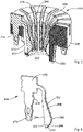
- an electrical connector 240 is shown to include a dielectric or electrically insulative connector housing 242 having a generally cylindrical shape and a plurality of electrical terminals 244 supported by connector housing 242.
- Housing 242 defines an opening 246 to a receiving chamber 247. The diameter of opening 246 is preferably sized to permit passage of a power plug into chamber 247.
- Housing 242 includes a generally cylindrical base portion 248 and a generally cylindrical central portion 250 extending from base portion 248. Base portion 248 and central portion 250 together define chamber 247.
- portions 248 and 250 are shown to be monolithic, it should be appreciated, unless otherwise indicated, that such components can be separate from one another.
- Central portion 250 includes a frustoconical outer surface 252 where the outer surface diameter of portion 250 becomes smaller along the length of portion 250 extending away from base portion 248.
- Housing 242 is also shown to define an angled surface 254 surrounding opening 246.
- Surface 254 also acts to locate and center a plug being inserted into connector 240.
- Opening 246, the receiving chamber and angled surface 254 preferably are centered about an insertion axis 255.
- Terminal 244 is an electrically conductive monolithic body. It should be appreciated, however, unless otherwise indicated, that various components of the terminal 244 can be separate from one or more other components of the terminal as desired.
- the terminal 244 is constructed in a stamping operation. In such an operation sheet metal, which can be stainless steel, tin, copper, alloys including the same, or any alternative suitable electrically conductive material, is stamped to form the terminal 244,
- sheet metal which can be stainless steel, tin, copper, alloys including the same, or any alternative suitable electrically conductive material, is stamped to form the terminal 244,
- a plurality of terminals is formed from a single sheet of material and is supported by a common carrier strip.
- the stamped electrical terminals and the carrier strip can be monolithic with each other.
- the electrical terminals can be separated from the carrier strip in the usual manner.
- the power terminal 244 includes a base 256 and a contact beam 258 that extends from the base 256.
- Base 256 and contact beam 258 are monolithic with each other.
- the contact beam 258 defines a contact portion 260 that is configured to contact a complementary electrical power terminal that is mated with the power terminal 240.
- the complementary power terminal can be supported by a plug housing of a plug connector that is received by a receptacle connector that includes the power terminal 240.
- the contact portion 260 includes a first side 262 and a second side 264, The first side 262 is referred to as a first contact side, and the second side 264 is referred to as a second contact side.
- the first side 262 is opposite the second side 264.
- first side 262 is spaced radially inward with respect to the second side 264 when the power terminal 244 is supported by connector housing 242,
- the first and second sides 262 and 264 are oriented at an angle relative to each other.
- the first side 262 is angled with respect to the second side 264.
- the first side 262 is angled relative to the second side 264 such that the width of terminal 244 or the distance from the first side 262 to the second side 264 becomes greater in a direction away from base 256. Otherwise stated, the first side 262 flares away from the second side 264 as it extends in a direction away from the base 256.
- the contact beam 258 further includes an insertion portion 266 disposed at the end of power terminal 244 furthest from base 256.
- the contact portion 260 is disposed between the base 256 and the insertion portion 266.
- the insertion portion 266 defines a first side 268 and a second side 270.
- the first side 268 is referred to as a first insertion side
- the second side 270 is referred to as a second insertion side.
- the first side 268 is opposite the second side 270.
- the first side 268 is spaced radially inward with respect to the second side 270 when the power terminal is supported by the connector housing 242,
- the first and second sides 268 and 270 are oriented at an angle relative to each other.
- first side 268 is angled relative to the second side 270 such that the width of terminal 244 or the distance from the first side 268 to the second side 270 becomes smaller along the insertion portion 266 in a direction away from base 256. It should thus be appreciated that the first side 262 of the contact portion 260 and the first side 268 of the insertion portion 266 join together at an interface that is defined by an apex of the contact beam 258.
- connector 240 is shown to include terminals 244 having tails 272 that are formed as press fit tails and which extend from base 256 in generally the same direction as contact beams 258, Tails 272 extend from base portion 248 in generally the same direction as beams 258, It is noted that each terminal 244 is positioned within one of a plurality of slots 274 formed in housing 242.
- terminals 244 can be held within slots 274 in any number of ways, the terminals are shown a toothed surface having one or more teeth 276 for engaging an inner wall within base portion 248 of slot 274 and holding terminal 244 in place, ft is noted that in order to allow beams 258 to flex upon insertion of a plug into cavity 247, the width of slot 274 within central portion 250 permits the movement of beam 258 within the slot.
- slots or passages 274 are depicted, it should be understood that housing 242 could also be formed on terminals 244 by an over-molding operation.
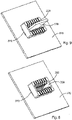
- connector 350 is similar to connector 240 except for its rectangular shape. Given the rectangular shape, connector 350 can function as a card edge connector or as a power connector. Electrical connector 350 is shown to include a dielectric or electrically insulative connector housing 352 having a rectangular shape and a plurality of electrical terminals 244, described previously, supported by connector housing 352. Electrical terminals 244 are preferably arranged in opposed pairs so that the beams 258 of each pair of terminals are positioned facing opposite to one another.
- Housing 352 defines an opening 354 to a receiving chamber 356.
- the width of opening 354 is preferably sized to permit passage of a card edge into chamber 356.
- Housing 352 includes a generally rectangular base portion 358 and a generally rectangular central portion 360 extending from base portion 358. Base portion 358 and central portion 360 together define chamber 356.
- portions 358 and 360 are shown to be monolithic, it should be appreciated, unless otherwise indicated, that such components can be separate from one another.
- Central portion 360 includes an outer surface 362 where the surfaces of the long sides are tapered so that, the outer surface of central portion 360 becomes narrower along the length of central portion 360 extending away from base portion 358.
- Housing 352 is also shown to define an angled surface 364 surrounding opening 356. Surface 364 also acts to locate and center a card or plug being inserted into connector 350.
- the housing 352 defines a first end and a second end.
- the opening 354 extends from the first end to the second end such that a mating contact, card edge, flat substrate, planar substrate, tab, bus bar tab, circuit board or card 378 can pass through the first end of the housing 352 and extend beyond the second end.
- the opening 354 can be aligned with a coincident opening in the substrate, circuit board or bus bar 370 such that the mating contact, card edge, flat substrate, planar substrate, tab, bus bar tab, circuit board or card 378 can pass through both the connector 350 and a plane, any portion, upper surface or bottom surface of the circuit board or bus bar 370.
- An insertion depth of the mating contact, card edge, flat substrate, planar substrate, tab, bus bar tab, circuit board or card 378 may be defined by a length of circuit board or card 378 that extends perpendicularly beyond the plane or bottom surface of the circuit board or bus bar 370 after the mating contact, card edge, flat substrate, planar substrate, tab, bus bar tab, circuit board or card 378 is fully mated with the connector 350 in a mating direction.
- the bottom surface is a second surface of the circuit board or bus bar 370 penetrated by the circuit board or card 378 during insertion of the circuit board or card 378 into the housing 352 and the circuit board or bus bar 370.
- the insertion depth or length of the mating contact, card edge, flat substrate, planar substrate, tab, bus bar tab, circuit board or card 378 that extends from the bottom surface of the circuit board or bus bar 370 can be adjusted as necessary by adding stops to the housing 352 or the mating contact, card edge, flat substrate, planar substrate, tab, bus bar tab, circuit board or card 378.
- the upper surface of the circuit board or bus bar 370 is penetrated first by the mating contact, card edge, flat substrate, planar substrate, tab, bus bar tab, circuit board or card 378 during insertion of the mating contact card edge, flat substrate, planar substrate, tab, bus bar tab, circuit board or card 378 into the housing 353 and the circuit board or bus bar 370. Any portion means any penetration of the mating contact, card edge, flat substrate, planar substrate, tab, bus bar tab, circuit board or card 378 beyond the upper surface of the circuit board or bus bar 370 in an insertion direction.
- Terminal 244 is an electrically conductive monolithic body. St should be appreciated, however, unless otherwise indicated, that various components of the terminal 244 can be separate from one or more other components of the terminal as desired.
- the terminal 244 is constructed in a stamping operation. In such an operation sheet metal, which can be stainless steel, tin, copper, alloys including the same, or any alternative suitable electrically conductive material, is stamped to form the terminal 244.
- sheet metal which can be stainless steel, tin, copper, alloys including the same, or any alternative suitable electrically conductive material, is stamped to form the terminal 244.
- a plurality of terminals is formed from a single sheet of material and is supported by a common carrier strip.
- the stamped electrical terminals and the carrier strip can be monolithic with each other.
- the electrical terminals can be separated from the earner strip in the usual manner.
- the power terminal 244 can include a base 256 and a contact beam 258 that extends from the base 256.
- Base 256 and contact beam 258 can be monolithic with each other.
- the contact beam 258 defines a contact portion 260 that is configured to contact a complementary electrical power terminal that is mated with the power terminal 240.
- the complementary' power terminal can be supported by a plug housing of a plug connector that is received by a receptacle connector that includes the power terminal 240.
- the contact portion 260 includes a first side 262 and a second side 264.
- the first side 262 can be referred to as a first, contact side, and the second side 264 can be referred to as a second contact side.
- the first side 262 can be opposite the second side 264.
- first side 262 can be spaced radially inward with respect to the second side 264 when the power terminal 244 is supported by connector housing 242.
- the first and second sides 262 and 264 can further be oriented at an angle relative to each other.
- the first side 262 can angled with respect to the second side 264.
- the first side 262 can be angled relative to the second side 264 such that the width of terminal 244 or the distance from the first side 262 to the second side 264 becomes greater in a direction away from base 256.
- the first side 262 can flare away from the second side 264 as it extends in a direction away from the base 256.
- the contact beam 258 can further include an insertion portion 266 disposed at the end of power terminal 244 furthest from base 256.
- the contact portion 260 can be disposed between the base 256 and the insertion portion 266.
- the insertion portion 266 can define a first side 268 and a second side 270.
- the first side 268 can be referred to as a first insertion side
- the second side 270 can be referred to as a second insertion side.
- the first side 268 can be opposite the second side 270.
- the first side 268 can be spaced radially inward with respect to the second side 270 when the power terminal is supported by the connector housing 242,
- the first and second sides 268 and 270 can further be oriented at an angle relative to each other.
- the first side 268 can be angled relative to the second side 270 such that the width of terminal 244 or the distance from the first side 268 to the second side 270 becomes smaller along the insertion portion 266 in a direction away from base 256. It should thus be appreciated that the first side 262 of the contact portion 260 and the first side 268 of the insertion portion 266 join together at an interface that can be defined by an apex of the contact beam 258.
- electrical terminals 244 have tails 272 that are formed as press fit tails and which extend from base 256 in generally the same direction as contact beams 258. As shown in Figs. 6 and 7 , tails 272 extend from base portion 358 in generally the same direction as beams 258. It is noted that each terminal 244 is positioned within one of a plurality of slots 366 formed in housing 352. Although terminals 244 can be held within slots 366 in any number of ways, it is again noted that the terminals include a toothed surface having one or more teeth 368 ( Fig.
- connector 350 could include terminals having tails that are directed away from base portion 358 at a sharp angle thereby providing a platform like arrangement to facilitate mounting connector 350 using surface mount techniques. It is also within the invention for the tails to include a shortened length or stub intended to cooperate with solder bails and the like to electrically connect terminal 244 to an electrical circuit.
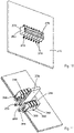
- electrical connector 350 is shown connected to a circuit board 370. As shown, central portion 360 passes through an opening 372 formed in board 370. Given that this particular embodiment includes terminals 244 having tails 272 formed as press fit tails, electrical connector 350 is mounted to circuit board 370 via a number of holes or vias 376 formed therein, an example of which is shown in Fig. 10 . It should be understood that the diameter of any holes or vias formed in board 370 for receiving tails 272 should be small enough to permit the press fit tails to at least frictionally engage the inner surface of such holes or vias.
- a circuit board or card 378 has been inserted through opening 354 and into chamber 356.
- the dimensions of chamber 356 and the distance between pairs of opposed terminals 244 are set so that beams 258 engage card 378 during insertion into chamber 356.
- card 378 includes electrically conductive pads formed on one of both surfaces and are positioned such that as card 378 is inserted such pads will be wiped by beams 258 of terminals 244 thereby establishing an electrical connection between the pads and terminals 244. More particularly, as shown in Fig. 11 , card 378 has only been partially inserted into connector 350 to the point where the leading edge of card 378 is making initial contact with opposed beams 258.
- beams 258 will be deflected. Since terminal 244 is preferably stamped from metal, the deflection of beams 258 will result in a compression force for beams 258 to return to their initial position. This force contributes to the resulting wiping of beams 258 against pads formed on card 378 thereby establishing an electrical connection between card 378 and terminals 244.
Landscapes
- Engineering & Computer Science (AREA)
- Manufacturing & Machinery (AREA)
- Coupling Device And Connection With Printed Circuit (AREA)
Claims (9)
- Connecteur d'alimentation (240, 350) comprenant :un boîtier de connecteur électriquement isolant (242, 352) définissant une chambre de réception (247, 356) configurée pour recevoir une fiche d'alimentation ; etune pluralité de bornes électriques (244) portées par le boîtier de connecteur, chacune des bornes électriques comportant :une base (256) ;une barre de contact (258) s'étendant à partir de ladite base, ladite barre de contact comportant une partie de contact (260), et une partie de montage qui s'étend à partir de ladite base et est monolithique avec ladite base pour le montage de ladite borne sur un substrat ;dans lequel ladite pluralité de bornes électriques sont positionnées dans ledit boîtier par rapport à ladite chambre de réception de sorte que ladite au moins une partie de ladite partie de contact s'étende dans ladite chambre, afin que le connecteur d'alimentation soit configuré pour loger des fiches d'alimentation de tailles variables,caractérisé en ce que la barre de contact comprend en outre une partie d'insertion (266), la partie de contact étant disposée entre la base et la partie d'insertion, dans lequel la partie de contact (260) comprend un premier côté de contact (262) et un second côté de contact (264) opposé, et le premier côté de contact de la partie de contact s'évase par rapport au second côté de contact de la partie de contact à mesure qu'il s'étend dans une direction en éloignement par rapport à la base, dans lequel la partie d'insertion comprend un premier côté d'insertion (268) et un second côté d'insertion (270), et le premier côté d'insertion de la partie d'insertion est incliné par rapport au second côté d'insertion de la partie d'insertion afin que la largeur de la borne d'alimentation électrique (244) devienne plus petite le long de la partie d'insertion dans une direction en éloignement par rapport à la base, et dans lequel le premier côté de contact de la partie de contact et le premier côté d'insertion de la partie d'insertion se rejoignent au niveau d'une interface qui peut être définie par un sommet de la barre de contact,dans lequel ladite chambre de réception (247, 356) définit un axe d'insertion et dans lequel ladite barre de contact s'étend en éloignement par rapport à ladite base selon un angle vers ledit axe d'insertion.
- Connecteur d'alimentation selon la revendication 1, dans lequel les bornes (244) comprennent des extrémités de montage (272) configurées sous la forme de queues à ajustement serré.
- Connecteur d'alimentation selon l'une quelconque des revendications 1 ou 2, dans lequel chacune des extrémités de montage (272) s'étend en éloignement par rapport à ladite base (256) dans une direction généralement parallèle à la barre de contact (258) vers une ouverture de la chambre de réception.
- Connecteur d'alimentation selon l'une quelconque des revendications précédentes, dans lequel la barre de contact (258) s'étend à partir de la base (256) dans une première direction, et les extrémités de montage (272) s'étendent à partir de la base dans la première direction.
- Connecteur d'alimentation selon l'une quelconque des revendications précédentes, dans lequel des parties de montage d'au moins certaines de la pluralité de bornes électriques (244) sont configurées pour se connecter électriquement au substrat.
- Connecteur d'alimentation selon l'une quelconque des revendications précédentes, dans lequel chacune de ladite pluralité de bornes électriques (244) comprend en outre une partie d'ancrage (276) configurée pour ancrer les bornes audit boîtier.
- Connecteur d'alimentation selon la revendication 8, dans lequel ledit boîtier électriquement isolant (242) définit des passages (274) pour la réception desdites bornes (244) et dans lequel ladite partie d'ancrage comporte une surface dentée (276) pour venir en contact avec une surface interne desdits passages.
- Connecteur d'alimentation selon l'une quelconque des revendications précédentes, monté sur un substrat.
- Connecteur d'alimentation selon l'une quelconque des revendications précédentes, dans lequel la pluralité de bornes électriques (244) sont agencées de manière cylindrique autour de l'axe d'insertion.
Applications Claiming Priority (2)
| Application Number | Priority Date | Filing Date | Title |
|---|---|---|---|
| US201462069037P | 2014-10-27 | 2014-10-27 | |
| PCT/US2015/057527 WO2016069570A2 (fr) | 2014-10-27 | 2015-10-27 | Connecteurs d'alimentation circulaires |
Publications (2)
| Publication Number | Publication Date |
|---|---|
| EP3213374A2 EP3213374A2 (fr) | 2017-09-06 |
| EP3213374B1 true EP3213374B1 (fr) | 2022-10-26 |
Family
ID=54477339
Family Applications (1)
| Application Number | Title | Priority Date | Filing Date |
|---|---|---|---|
| EP15790778.3A Active EP3213374B1 (fr) | 2014-10-27 | 2015-10-27 | Connecteur d'alimentation |
Country Status (5)
| Country | Link |
|---|---|
| US (3) | US10312647B2 (fr) |
| EP (1) | EP3213374B1 (fr) |
| CN (3) | CN116435805A (fr) |
| TW (1) | TWI618320B (fr) |
| WO (1) | WO2016069570A2 (fr) |
Families Citing this family (18)
| Publication number | Priority date | Publication date | Assignee | Title |
|---|---|---|---|---|
| TWI670012B (zh) * | 2014-07-28 | 2019-09-01 | 美商陶氏農業科學公司 | 具有某些殺蟲效用之分子及與其相關之中間物、組成物及方法 |
| WO2016069570A2 (fr) | 2014-10-27 | 2016-05-06 | Fci Asia Pte. Ltd | Connecteurs d'alimentation circulaires |
| KR102514524B1 (ko) * | 2016-11-17 | 2023-03-29 | 몰렉스 엘엘씨 | 부유식 소켓 커넥터 |
| CN109256637B (zh) * | 2017-07-13 | 2024-07-05 | 泰科电子(上海)有限公司 | 插座连接器和插拔插头连接器的方法 |
| DE102017213150A1 (de) * | 2017-07-31 | 2019-01-31 | Robert Bosch Gmbh | Elektrischer Steckkontakt für Hochstromanwendungen und Steckverbindersystem für Hochstromanwendungen |
| USD878304S1 (en) | 2018-06-29 | 2020-03-17 | Molex, Llc | Contact for a connector |
| USD867298S1 (en) * | 2018-06-29 | 2019-11-19 | Molex, Llc | Socket connector |
| USD877702S1 (en) * | 2018-06-29 | 2020-03-10 | Molex, Llc | Socket connector |
| USD868000S1 (en) * | 2018-06-30 | 2019-11-26 | Molex, Llc | Socket connector |
| USD868001S1 (en) * | 2018-06-30 | 2019-11-26 | Molex, Llc | Socket connector |
| USD867299S1 (en) * | 2018-07-06 | 2019-11-19 | Molex, Llc | Socket connector |
| USD868002S1 (en) * | 2018-07-06 | 2019-11-26 | Molex, Llc | Socket connector |
| USD936017S1 (en) * | 2019-03-06 | 2021-11-16 | Molex, Llc | Floating socket connector |
| US10680370B1 (en) * | 2019-03-26 | 2020-06-09 | Antaya Technologies Corporation | Electrical terminal, electrical connector assembly, and method of forming same |
| DE102019125783B4 (de) * | 2019-09-25 | 2025-08-14 | Audi Ag | Energieversorgungsanordnung zur Versorgung eines Kraftfahrzeugs mit elektrischer Energie über eine konduktive Steckverbindung sowie Verfahren zum Betreiben einer Energieversorgungsanordnung |
| US12401146B2 (en) | 2019-12-12 | 2025-08-26 | Fci Usa Llc | Card-edge connector system with busbar connection for high-power applications |
| US12176637B2 (en) | 2021-02-09 | 2024-12-24 | Fci Usa Llc | Electrical connector for high power computing system |
| US12525755B2 (en) * | 2021-07-19 | 2026-01-13 | Fci Usa Llc | Power connector for compact electronic systems |
Family Cites Families (96)
| Publication number | Priority date | Publication date | Assignee | Title |
|---|---|---|---|---|
| US3172718A (en) * | 1963-03-20 | 1965-03-09 | Electronic Fittings Corp | Multiple contact receptacle for printed circuit boards and the like |
| US3760329A (en) * | 1972-08-03 | 1973-09-18 | Gtl Automatic Electric Labor I | Mated connector apparatus for printed wiring boards |
| FR2252728B2 (fr) * | 1973-11-22 | 1976-11-19 | Honeywell Bull Soc Ind | |
| US4077694A (en) * | 1975-06-24 | 1978-03-07 | Amp Incorporated | Circuit board connector |
| CA1070792A (fr) * | 1976-07-26 | 1980-01-29 | Earl A. Cooper | Connecteur electrique, dispositif antiparasite et methode de fabrication |
| US4377320A (en) * | 1980-11-26 | 1983-03-22 | Amp Incorporated | Coaxial connector |
| US4538878A (en) * | 1983-08-12 | 1985-09-03 | Molex Incorporated | Solderless circuit board connector |
| US4891476A (en) * | 1988-05-09 | 1990-01-02 | Illinois Tool Works, Inc. | Index rotary switch |
| US4946403A (en) * | 1989-08-24 | 1990-08-07 | Amp Incorporated | Low insertion force circuit panel socket |
| US5024609A (en) * | 1990-04-04 | 1991-06-18 | Burndy Corporation | High-density bi-level card edge connector and method of making the same |
| US5030107A (en) * | 1990-11-08 | 1991-07-09 | Molex Incorporated | LCD cluster connector |
| US5199895A (en) * | 1992-02-04 | 1993-04-06 | Chang Lien Ker | Low insertion force, self-locking connecting apparatus for electrically connecting memory modules to a printed circuit board |
| JPH05299144A (ja) * | 1992-04-18 | 1993-11-12 | Molex Inc | 電気コネクタ |
| SG47417A1 (en) * | 1993-11-15 | 1998-04-17 | Connector Systems Tech Nv | Solderable connectors for high density electronic assemblies |
| US5533907A (en) * | 1994-05-27 | 1996-07-09 | Methode Electronics, Inc. | Electronic module socket with self-cleaning shorting contacts |
| US6220878B1 (en) * | 1995-10-04 | 2001-04-24 | Methode Electronics, Inc. | Optoelectronic module with grounding means |
| US5997367A (en) * | 1995-06-05 | 1999-12-07 | Vlt Corporation | Adapter |
| JP3744047B2 (ja) * | 1996-02-13 | 2006-02-08 | オートスプライス株式会社 | 多極小型雄コネクタと多極小型雌コネクタ及びそれを用いた多極小型コネクタ |
| JP3028199B2 (ja) * | 1996-03-14 | 2000-04-04 | モレックス インコーポレーテッド | 電気コネクタのターミナル |
| US5836773A (en) * | 1996-07-29 | 1998-11-17 | Hon Hai Precision Ind. Co., Ltd. | Board-to-board connector |
| US5911595A (en) * | 1996-07-29 | 1999-06-15 | Kern Engineering & Mfg. Co. | Low profile angular connector device and method |
| US6012936A (en) * | 1996-10-16 | 2000-01-11 | The Siemon Company | Switching jack |
| US5931689A (en) * | 1997-08-06 | 1999-08-03 | Molex Incorporated | Electric connector assembly with improved locking characteristics |
| US6139351A (en) * | 1999-06-16 | 2000-10-31 | Delphi Technologies, Inc. | High power connection system |
| JP2001210419A (ja) * | 2000-01-25 | 2001-08-03 | Tyco Electronics Amp Kk | 雌型端子 |
| US6425766B1 (en) * | 2000-06-09 | 2002-07-30 | Molex Incorporated | Impedance control in edge card connector systems |
| TW476466U (en) * | 2000-09-29 | 2002-02-11 | Hon Hai Prec Ind Co Ltd | Electrical connector |
| US6450829B1 (en) * | 2000-12-15 | 2002-09-17 | Tyco Electronics Canada, Ltd. | Snap-on plug coaxial connector |
| JP3909213B2 (ja) * | 2001-02-06 | 2007-04-25 | 矢崎総業株式会社 | 基板用コネクタ |
| TW499063U (en) * | 2001-03-27 | 2002-08-11 | Hon Hai Prec Ind Co Ltd | Power connector |
| US6461174B1 (en) * | 2001-09-12 | 2002-10-08 | Hon Hai Precision Ind. Co., Ltd. | Power connector more easily and cheaply manufactured |
| JP3901501B2 (ja) * | 2001-12-12 | 2007-04-04 | アルプス電気株式会社 | 電子回路ユニットの取付構造 |
| TW529827U (en) * | 2002-04-30 | 2003-04-21 | Hon Hai Prec Ind Co Ltd | Power connector |
| JP3745318B2 (ja) | 2002-07-24 | 2006-02-15 | タイコエレクトロニクスアンプ株式会社 | 電気コネクタ組立体 |
| JP3761501B2 (ja) * | 2002-07-31 | 2006-03-29 | 本多通信工業株式会社 | 同軸コネクタ及びそれが実装されるグランドパッド |
| TWM245634U (en) * | 2002-12-02 | 2004-10-01 | Starlink Electronics Corp | Electrical connector terminal |
| JP4181895B2 (ja) | 2003-02-25 | 2008-11-19 | 日本圧着端子製造株式会社 | リセプタクル |
| US7070446B2 (en) * | 2003-08-27 | 2006-07-04 | Tyco Electronics Corporation | Stacked SFP connector and cage assembly |
| CN2850023Y (zh) * | 2005-11-04 | 2006-12-20 | 富士康(昆山)电脑接插件有限公司 | 电连接器 |
| TWM302146U (en) * | 2006-04-24 | 2006-12-01 | Hon Hai Prec Ind Co Ltd | Electrical connector |
| CN200965632Y (zh) | 2006-08-25 | 2007-10-24 | 杭州洋驰科技有限公司 | 袜机控制系统 |
| CN200965932Y (zh) * | 2006-11-14 | 2007-10-24 | 莫列斯公司 | 电连接器 |
| US7413456B1 (en) * | 2006-11-14 | 2008-08-19 | Difusco Frank | Quick connect light bulb socket |
| TWM314962U (en) * | 2007-01-22 | 2007-07-01 | Nextronics Engineering Corp | Press-type power connector |
| JP4971857B2 (ja) * | 2007-03-29 | 2012-07-11 | 富士通コンポーネント株式会社 | コネクタ装置 |
| KR101380305B1 (ko) * | 2007-06-22 | 2014-04-03 | 삼성디스플레이 주식회사 | 백라이트 어셈블리 |
| US8038465B2 (en) * | 2008-01-07 | 2011-10-18 | Lear Corporation | Electrical connector and heat sink |
| US7806737B2 (en) * | 2008-02-04 | 2010-10-05 | Methode Electronics, Inc. | Stamped beam connector |
| CN101505017B (zh) * | 2008-02-04 | 2013-07-10 | 凡甲电子(苏州)有限公司 | 电源连接器组件 |
| JP5001201B2 (ja) * | 2008-03-07 | 2012-08-15 | 富士通コンポーネント株式会社 | コネクタ装置及びコネクタ装置の接続方法 |
| CN101551500B (zh) * | 2008-04-03 | 2012-02-01 | 富准精密工业(深圳)有限公司 | 相机模组 |
| CN101572359B (zh) * | 2008-04-30 | 2013-06-05 | 凡甲电子(苏州)有限公司 | 电源连接器及其端子复合悬臂梁结构 |
| US7708563B2 (en) * | 2008-06-18 | 2010-05-04 | Tyco Electronics Corporation | Electrical connector with slotted shield |
| CN101621168A (zh) * | 2008-06-30 | 2010-01-06 | 长盛科技股份有限公司 | 音频连接器 |
| US7597580B1 (en) * | 2008-09-17 | 2009-10-06 | Yazaki North America, Inc. | Connector with terminal motion reduction |
| JP5343497B2 (ja) * | 2008-10-01 | 2013-11-13 | オムロン株式会社 | コネクタ用接続端子およびそれを組み込んだコネクタ |
| CN101764294B (zh) * | 2008-12-26 | 2013-09-04 | 松富电子(深圳)有限公司 | 电连接器 |
| CN201430276Y (zh) * | 2009-04-23 | 2010-03-24 | 富士康(昆山)电脑接插件有限公司 | 电连接器组件 |
| CN102474056B (zh) * | 2009-07-31 | 2014-10-15 | 株式会社藤仓 | 同轴连接器 |
| JP5080692B2 (ja) * | 2009-09-01 | 2012-11-21 | オリンパスメディカルシステムズ株式会社 | 電気コネクタ及び内視鏡 |
| WO2011061579A1 (fr) * | 2009-11-23 | 2011-05-26 | Abb Technology Ltd | Procédé et système permettant de mettre à niveau un disjoncteur |
| JP5434748B2 (ja) * | 2009-12-24 | 2014-03-05 | 日立金属株式会社 | 車両用導電路 |
| US8052454B2 (en) * | 2009-12-31 | 2011-11-08 | Hon Hai Precision Ind. Co., Ltd. | Electrical connector with improved feature for securing solder ball thereon |
| DE102010002681B4 (de) * | 2010-03-09 | 2018-10-18 | Te Connectivity Germany Gmbh | Elektrischer Steckverbinder, elektrische Steckverbindung sowie konfektioniertes elektrisches Kabel |
| SG174646A1 (en) * | 2010-03-26 | 2011-10-28 | Molex Inc | Card edge connector and connector assembly thereof |
| US8057263B1 (en) * | 2010-07-12 | 2011-11-15 | Tyco Electronics Corporation | Edge connectors having stamped signal contacts |
| EP2418666A1 (fr) * | 2010-08-13 | 2012-02-15 | ABB Technology AG | Agencement de contact électrique, spécialement pour un disjoncteur à moyenne tension aéro-isolé |
| CN103069653B (zh) * | 2010-08-19 | 2016-10-26 | 富加宜汽车控股公司 | 电源端子 |
| US20120089203A1 (en) * | 2010-10-12 | 2012-04-12 | Advanced Neuromodulation Systems, Inc. | Electrical connections for use in implantable medical devices |
| WO2012061142A2 (fr) * | 2010-10-25 | 2012-05-10 | Molex Incorporated | Cadre d'adaptateur présentant des fonctions de prise et d'interférences électromagnétiques intégrées |
| CN102544836A (zh) * | 2010-12-16 | 2012-07-04 | 陕西四菱电子有限责任公司 | 一种通用插孔接触件 |
| US8783368B2 (en) * | 2011-01-05 | 2014-07-22 | Schlumberger Technology Corporation | Well tool with shearable collet |
| US9325095B2 (en) * | 2011-05-05 | 2016-04-26 | Lear Corporation | Female type contact for an electrical connector |
| JP5743740B2 (ja) * | 2011-06-23 | 2015-07-01 | 矢崎総業株式会社 | コネクタ |
| JP5902895B2 (ja) * | 2011-06-29 | 2016-04-13 | 矢崎総業株式会社 | シールド電線の固定構造 |
| US8376766B1 (en) * | 2011-08-16 | 2013-02-19 | International Business Machines Corporation | Connector with compliant section |
| CN103390812A (zh) | 2012-05-10 | 2013-11-13 | 凡甲电子(苏州)有限公司 | 电连接器 |
| JP2014086349A (ja) * | 2012-10-25 | 2014-05-12 | Sumitomo Wiring Syst Ltd | コネクタ |
| CN204884912U (zh) * | 2012-11-07 | 2015-12-16 | Abb技术有限公司 | 接触指形元件、接触组件、切换装置和开关设备 |
| US8956186B2 (en) * | 2013-03-13 | 2015-02-17 | Tyco Electronics Corporation | Right angle header assembly |
| JP6092694B2 (ja) * | 2013-04-12 | 2017-03-08 | 日本圧着端子製造株式会社 | コネクタ |
| ES2635625T3 (es) * | 2013-07-30 | 2017-10-04 | Abb Schweiz Ag | Dispositivo de conexión para un aparato conmutador |
| US9287656B2 (en) * | 2013-11-11 | 2016-03-15 | Amphenol Corporation | Heat dissipating electrical connector |
| JP6076505B2 (ja) * | 2014-01-20 | 2017-02-08 | 矢崎総業株式会社 | 活電部保護構造及びコネクタ |
| DE102014220016A1 (de) * | 2014-10-02 | 2016-04-07 | Sumitomo Electric Bordnetze Gmbh | Vorrichtung zum elektromagnetisch verträglichen Verbinden von elektrischen Leitern mit Abschirmungsschicht |
| WO2016069570A2 (fr) | 2014-10-27 | 2016-05-06 | Fci Asia Pte. Ltd | Connecteurs d'alimentation circulaires |
| US9620265B2 (en) * | 2015-01-21 | 2017-04-11 | Te Connectivity Corporation | Sealed header assembly |
| US9455523B1 (en) * | 2015-08-05 | 2016-09-27 | Delphi Technologies, Inc. | Right angle connection assembly |
| US9559467B1 (en) * | 2015-08-17 | 2017-01-31 | Foxconn Interconnect Technology Limited | Connector assembly with reliable electrical connection |
| US10574001B2 (en) * | 2016-01-13 | 2020-02-25 | Molex, Llc | High power electrical connector |
| US10203228B2 (en) * | 2016-07-20 | 2019-02-12 | Veoneer Us, Inc. | Crash sensor assembly |
| US10514092B2 (en) * | 2016-12-19 | 2019-12-24 | Eaton Corporation | Position sensor body assembly |
| JP6527911B2 (ja) * | 2017-06-09 | 2019-06-12 | 矢崎総業株式会社 | コネクタ |
| US10573988B2 (en) * | 2017-08-01 | 2020-02-25 | Delphi Technologies, Llc | Cable assembly with strain relief |
| US10396486B2 (en) * | 2017-12-01 | 2019-08-27 | Te Connectivity India Private Limited | Electrical connector with terminal position assurance member |
| US11753900B2 (en) * | 2020-07-20 | 2023-09-12 | Halliburton Energy Services, Inc. | Activation of downhole mechanical device with inclination and/or change in RPM |
-
2015
- 2015-10-27 WO PCT/US2015/057527 patent/WO2016069570A2/fr not_active Ceased
- 2015-10-27 US US15/522,637 patent/US10312647B2/en active Active
- 2015-10-27 CN CN202310622876.9A patent/CN116435805A/zh active Pending
- 2015-10-27 TW TW104135296A patent/TWI618320B/zh not_active IP Right Cessation
- 2015-10-27 CN CN201580069759.8A patent/CN107112674B/zh active Active
- 2015-10-27 CN CN202010928319.6A patent/CN111987497B/zh active Active
- 2015-10-27 EP EP15790778.3A patent/EP3213374B1/fr active Active
-
2019
- 2019-05-31 US US16/427,943 patent/US10862253B2/en active Active
-
2020
- 2020-12-07 US US17/114,074 patent/US11616329B2/en active Active
Also Published As
| Publication number | Publication date |
|---|---|
| EP3213374A2 (fr) | 2017-09-06 |
| US11616329B2 (en) | 2023-03-28 |
| WO2016069570A3 (fr) | 2016-06-30 |
| CN111987497A (zh) | 2020-11-24 |
| TWI618320B (zh) | 2018-03-11 |
| CN116435805A (zh) | 2023-07-14 |
| TW201626663A (zh) | 2016-07-16 |
| US20190288466A1 (en) | 2019-09-19 |
| US20170338606A1 (en) | 2017-11-23 |
| US10312647B2 (en) | 2019-06-04 |
| CN111987497B (zh) | 2023-06-16 |
| US10862253B2 (en) | 2020-12-08 |
| WO2016069570A2 (fr) | 2016-05-06 |
| US20210194192A1 (en) | 2021-06-24 |
| CN107112674B (zh) | 2020-10-09 |
| CN107112674A (zh) | 2017-08-29 |
Similar Documents
| Publication | Publication Date | Title |
|---|---|---|
| EP3213374B1 (fr) | Connecteur d'alimentation | |
| US9768527B2 (en) | Single element wire to board connector | |
| US7864544B2 (en) | Printed circuit board assembly | |
| US8109783B2 (en) | Insulation displacement connector (IDC) | |
| US9543664B2 (en) | Insulation displacement connector | |
| EP3007276B1 (fr) | Connecteur à élément unique | |
| US9306297B2 (en) | Interlocking poke home contact | |
| US9362630B2 (en) | Wire to board terminal | |
| US8608512B2 (en) | Cable connector | |
| JP2017212209A (ja) | 圧入回路基板コネクタ | |
| GB2516555A (en) | Single element wire to board connector | |
| TW202112005A (zh) | 安全、堅固且緊密之連接器 | |
| EP0499436B1 (fr) | Hameçon poussoir | |
| EP0954058A2 (fr) | Assemblage de connecteur électrique pour des circuits flexibles | |
| HK1220045B (en) | Single element connector | |
| JPH04131865U (ja) | 保持脚付電気コネクタ及び電気コネクタ用保持脚 | |
| HK1167751A (en) | Insulation displacement connector (idc) |
Legal Events
| Date | Code | Title | Description |
|---|---|---|---|
| STAA | Information on the status of an ep patent application or granted ep patent |
Free format text: STATUS: THE INTERNATIONAL PUBLICATION HAS BEEN MADE |
|
| PUAI | Public reference made under article 153(3) epc to a published international application that has entered the european phase |
Free format text: ORIGINAL CODE: 0009012 |
|
| STAA | Information on the status of an ep patent application or granted ep patent |
Free format text: STATUS: REQUEST FOR EXAMINATION WAS MADE |
|
| 17P | Request for examination filed |
Effective date: 20170519 |
|
| AK | Designated contracting states |
Kind code of ref document: A2 Designated state(s): AL AT BE BG CH CY CZ DE DK EE ES FI FR GB GR HR HU IE IS IT LI LT LU LV MC MK MT NL NO PL PT RO RS SE SI SK SM TR |
|
| AX | Request for extension of the european patent |
Extension state: BA ME |
|
| DAV | Request for validation of the european patent (deleted) | ||
| DAX | Request for extension of the european patent (deleted) | ||
| STAA | Information on the status of an ep patent application or granted ep patent |
Free format text: STATUS: EXAMINATION IS IN PROGRESS |
|
| 17Q | First examination report despatched |
Effective date: 20190522 |
|
| RIC1 | Information provided on ipc code assigned before grant |
Ipc: H01R 13/17 20060101ALI20220311BHEP Ipc: H01R 27/00 20060101ALI20220311BHEP Ipc: H01R 12/71 20110101ALI20220311BHEP Ipc: H01R 12/55 20110101ALI20220311BHEP Ipc: H01R 13/11 20060101AFI20220311BHEP |
|
| GRAP | Despatch of communication of intention to grant a patent |
Free format text: ORIGINAL CODE: EPIDOSNIGR1 |
|
| STAA | Information on the status of an ep patent application or granted ep patent |
Free format text: STATUS: GRANT OF PATENT IS INTENDED |
|
| INTG | Intention to grant announced |
Effective date: 20220517 |
|
| GRAS | Grant fee paid |
Free format text: ORIGINAL CODE: EPIDOSNIGR3 |
|
| GRAA | (expected) grant |
Free format text: ORIGINAL CODE: 0009210 |
|
| STAA | Information on the status of an ep patent application or granted ep patent |
Free format text: STATUS: THE PATENT HAS BEEN GRANTED |
|
| AK | Designated contracting states |
Kind code of ref document: B1 Designated state(s): AL AT BE BG CH CY CZ DE DK EE ES FI FR GB GR HR HU IE IS IT LI LT LU LV MC MK MT NL NO PL PT RO RS SE SI SK SM TR |
|
| REG | Reference to a national code |
Ref country code: GB Ref legal event code: FG4D |
|
| REG | Reference to a national code |
Ref country code: CH Ref legal event code: EP |
|
| REG | Reference to a national code |
Ref country code: DE Ref legal event code: R096 Ref document number: 602015081334 Country of ref document: DE |
|
| REG | Reference to a national code |
Ref country code: AT Ref legal event code: REF Ref document number: 1527744 Country of ref document: AT Kind code of ref document: T Effective date: 20221115 |
|
| REG | Reference to a national code |
Ref country code: IE Ref legal event code: FG4D |
|
| REG | Reference to a national code |
Ref country code: LT Ref legal event code: MG9D |
|
| REG | Reference to a national code |
Ref country code: NL Ref legal event code: MP Effective date: 20221026 |
|
| REG | Reference to a national code |
Ref country code: AT Ref legal event code: MK05 Ref document number: 1527744 Country of ref document: AT Kind code of ref document: T Effective date: 20221026 |
|
| PG25 | Lapsed in a contracting state [announced via postgrant information from national office to epo] |
Ref country code: NL Free format text: LAPSE BECAUSE OF FAILURE TO SUBMIT A TRANSLATION OF THE DESCRIPTION OR TO PAY THE FEE WITHIN THE PRESCRIBED TIME-LIMIT Effective date: 20221026 |
|
| PG25 | Lapsed in a contracting state [announced via postgrant information from national office to epo] |
Ref country code: SE Free format text: LAPSE BECAUSE OF FAILURE TO SUBMIT A TRANSLATION OF THE DESCRIPTION OR TO PAY THE FEE WITHIN THE PRESCRIBED TIME-LIMIT Effective date: 20221026 Ref country code: PT Free format text: LAPSE BECAUSE OF FAILURE TO SUBMIT A TRANSLATION OF THE DESCRIPTION OR TO PAY THE FEE WITHIN THE PRESCRIBED TIME-LIMIT Effective date: 20230227 Ref country code: NO Free format text: LAPSE BECAUSE OF FAILURE TO SUBMIT A TRANSLATION OF THE DESCRIPTION OR TO PAY THE FEE WITHIN THE PRESCRIBED TIME-LIMIT Effective date: 20230126 Ref country code: LT Free format text: LAPSE BECAUSE OF FAILURE TO SUBMIT A TRANSLATION OF THE DESCRIPTION OR TO PAY THE FEE WITHIN THE PRESCRIBED TIME-LIMIT Effective date: 20221026 Ref country code: FI Free format text: LAPSE BECAUSE OF FAILURE TO SUBMIT A TRANSLATION OF THE DESCRIPTION OR TO PAY THE FEE WITHIN THE PRESCRIBED TIME-LIMIT Effective date: 20221026 Ref country code: ES Free format text: LAPSE BECAUSE OF FAILURE TO SUBMIT A TRANSLATION OF THE DESCRIPTION OR TO PAY THE FEE WITHIN THE PRESCRIBED TIME-LIMIT Effective date: 20221026 Ref country code: AT Free format text: LAPSE BECAUSE OF FAILURE TO SUBMIT A TRANSLATION OF THE DESCRIPTION OR TO PAY THE FEE WITHIN THE PRESCRIBED TIME-LIMIT Effective date: 20221026 |
|
| PG25 | Lapsed in a contracting state [announced via postgrant information from national office to epo] |
Ref country code: RS Free format text: LAPSE BECAUSE OF FAILURE TO SUBMIT A TRANSLATION OF THE DESCRIPTION OR TO PAY THE FEE WITHIN THE PRESCRIBED TIME-LIMIT Effective date: 20221026 Ref country code: PL Free format text: LAPSE BECAUSE OF FAILURE TO SUBMIT A TRANSLATION OF THE DESCRIPTION OR TO PAY THE FEE WITHIN THE PRESCRIBED TIME-LIMIT Effective date: 20221026 Ref country code: LV Free format text: LAPSE BECAUSE OF FAILURE TO SUBMIT A TRANSLATION OF THE DESCRIPTION OR TO PAY THE FEE WITHIN THE PRESCRIBED TIME-LIMIT Effective date: 20221026 Ref country code: IS Free format text: LAPSE BECAUSE OF FAILURE TO SUBMIT A TRANSLATION OF THE DESCRIPTION OR TO PAY THE FEE WITHIN THE PRESCRIBED TIME-LIMIT Effective date: 20230226 Ref country code: HR Free format text: LAPSE BECAUSE OF FAILURE TO SUBMIT A TRANSLATION OF THE DESCRIPTION OR TO PAY THE FEE WITHIN THE PRESCRIBED TIME-LIMIT Effective date: 20221026 Ref country code: GR Free format text: LAPSE BECAUSE OF FAILURE TO SUBMIT A TRANSLATION OF THE DESCRIPTION OR TO PAY THE FEE WITHIN THE PRESCRIBED TIME-LIMIT Effective date: 20230127 |
|
| REG | Reference to a national code |
Ref country code: CH Ref legal event code: PL |
|
| P01 | Opt-out of the competence of the unified patent court (upc) registered |
Effective date: 20230517 |
|
| REG | Reference to a national code |
Ref country code: BE Ref legal event code: MM Effective date: 20221031 |
|
| PG25 | Lapsed in a contracting state [announced via postgrant information from national office to epo] |
Ref country code: LU Free format text: LAPSE BECAUSE OF NON-PAYMENT OF DUE FEES Effective date: 20221027 |
|
| REG | Reference to a national code |
Ref country code: DE Ref legal event code: R097 Ref document number: 602015081334 Country of ref document: DE |
|
| PG25 | Lapsed in a contracting state [announced via postgrant information from national office to epo] |
Ref country code: SM Free format text: LAPSE BECAUSE OF FAILURE TO SUBMIT A TRANSLATION OF THE DESCRIPTION OR TO PAY THE FEE WITHIN THE PRESCRIBED TIME-LIMIT Effective date: 20221026 Ref country code: RO Free format text: LAPSE BECAUSE OF FAILURE TO SUBMIT A TRANSLATION OF THE DESCRIPTION OR TO PAY THE FEE WITHIN THE PRESCRIBED TIME-LIMIT Effective date: 20221026 Ref country code: MC Free format text: LAPSE BECAUSE OF FAILURE TO SUBMIT A TRANSLATION OF THE DESCRIPTION OR TO PAY THE FEE WITHIN THE PRESCRIBED TIME-LIMIT Effective date: 20221026 Ref country code: LI Free format text: LAPSE BECAUSE OF NON-PAYMENT OF DUE FEES Effective date: 20221031 Ref country code: EE Free format text: LAPSE BECAUSE OF FAILURE TO SUBMIT A TRANSLATION OF THE DESCRIPTION OR TO PAY THE FEE WITHIN THE PRESCRIBED TIME-LIMIT Effective date: 20221026 Ref country code: DK Free format text: LAPSE BECAUSE OF FAILURE TO SUBMIT A TRANSLATION OF THE DESCRIPTION OR TO PAY THE FEE WITHIN THE PRESCRIBED TIME-LIMIT Effective date: 20221026 Ref country code: CZ Free format text: LAPSE BECAUSE OF FAILURE TO SUBMIT A TRANSLATION OF THE DESCRIPTION OR TO PAY THE FEE WITHIN THE PRESCRIBED TIME-LIMIT Effective date: 20221026 Ref country code: CH Free format text: LAPSE BECAUSE OF NON-PAYMENT OF DUE FEES Effective date: 20221031 |
|
| PG25 | Lapsed in a contracting state [announced via postgrant information from national office to epo] |
Ref country code: SK Free format text: LAPSE BECAUSE OF FAILURE TO SUBMIT A TRANSLATION OF THE DESCRIPTION OR TO PAY THE FEE WITHIN THE PRESCRIBED TIME-LIMIT Effective date: 20221026 Ref country code: AL Free format text: LAPSE BECAUSE OF FAILURE TO SUBMIT A TRANSLATION OF THE DESCRIPTION OR TO PAY THE FEE WITHIN THE PRESCRIBED TIME-LIMIT Effective date: 20221026 |
|
| PLBE | No opposition filed within time limit |
Free format text: ORIGINAL CODE: 0009261 |
|
| STAA | Information on the status of an ep patent application or granted ep patent |
Free format text: STATUS: NO OPPOSITION FILED WITHIN TIME LIMIT |
|
| PG25 | Lapsed in a contracting state [announced via postgrant information from national office to epo] |
Ref country code: BE Free format text: LAPSE BECAUSE OF NON-PAYMENT OF DUE FEES Effective date: 20221031 |
|
| 26N | No opposition filed |
Effective date: 20230727 |
|
| PG25 | Lapsed in a contracting state [announced via postgrant information from national office to epo] |
Ref country code: IE Free format text: LAPSE BECAUSE OF NON-PAYMENT OF DUE FEES Effective date: 20221027 |
|
| PG25 | Lapsed in a contracting state [announced via postgrant information from national office to epo] |
Ref country code: SI Free format text: LAPSE BECAUSE OF FAILURE TO SUBMIT A TRANSLATION OF THE DESCRIPTION OR TO PAY THE FEE WITHIN THE PRESCRIBED TIME-LIMIT Effective date: 20221026 |
|
| PG25 | Lapsed in a contracting state [announced via postgrant information from national office to epo] |
Ref country code: HU Free format text: LAPSE BECAUSE OF FAILURE TO SUBMIT A TRANSLATION OF THE DESCRIPTION OR TO PAY THE FEE WITHIN THE PRESCRIBED TIME-LIMIT; INVALID AB INITIO Effective date: 20151027 |
|
| PG25 | Lapsed in a contracting state [announced via postgrant information from national office to epo] |
Ref country code: CY Free format text: LAPSE BECAUSE OF FAILURE TO SUBMIT A TRANSLATION OF THE DESCRIPTION OR TO PAY THE FEE WITHIN THE PRESCRIBED TIME-LIMIT Effective date: 20221026 |
|
| PG25 | Lapsed in a contracting state [announced via postgrant information from national office to epo] |
Ref country code: MK Free format text: LAPSE BECAUSE OF FAILURE TO SUBMIT A TRANSLATION OF THE DESCRIPTION OR TO PAY THE FEE WITHIN THE PRESCRIBED TIME-LIMIT Effective date: 20221026 Ref country code: IT Free format text: LAPSE BECAUSE OF FAILURE TO SUBMIT A TRANSLATION OF THE DESCRIPTION OR TO PAY THE FEE WITHIN THE PRESCRIBED TIME-LIMIT Effective date: 20221026 |
|
| PG25 | Lapsed in a contracting state [announced via postgrant information from national office to epo] |
Ref country code: BG Free format text: LAPSE BECAUSE OF FAILURE TO SUBMIT A TRANSLATION OF THE DESCRIPTION OR TO PAY THE FEE WITHIN THE PRESCRIBED TIME-LIMIT Effective date: 20221026 |
|
| PG25 | Lapsed in a contracting state [announced via postgrant information from national office to epo] |
Ref country code: MT Free format text: LAPSE BECAUSE OF FAILURE TO SUBMIT A TRANSLATION OF THE DESCRIPTION OR TO PAY THE FEE WITHIN THE PRESCRIBED TIME-LIMIT Effective date: 20221026 |
|
| PG25 | Lapsed in a contracting state [announced via postgrant information from national office to epo] |
Ref country code: TR Free format text: LAPSE BECAUSE OF FAILURE TO SUBMIT A TRANSLATION OF THE DESCRIPTION OR TO PAY THE FEE WITHIN THE PRESCRIBED TIME-LIMIT Effective date: 20221026 |
|
| PGFP | Annual fee paid to national office [announced via postgrant information from national office to epo] |
Ref country code: DE Payment date: 20251029 Year of fee payment: 11 |
|
| PGFP | Annual fee paid to national office [announced via postgrant information from national office to epo] |
Ref country code: GB Payment date: 20251027 Year of fee payment: 11 |
|
| PGFP | Annual fee paid to national office [announced via postgrant information from national office to epo] |
Ref country code: FR Payment date: 20251027 Year of fee payment: 11 |