EP3214700A1 - Dispositif d'antenne intelligent - Google Patents
Dispositif d'antenne intelligent Download PDFInfo
- Publication number
- EP3214700A1 EP3214700A1 EP15854044.3A EP15854044A EP3214700A1 EP 3214700 A1 EP3214700 A1 EP 3214700A1 EP 15854044 A EP15854044 A EP 15854044A EP 3214700 A1 EP3214700 A1 EP 3214700A1
- Authority
- EP
- European Patent Office
- Prior art keywords
- antenna array
- radio frequency
- coupling
- dielectric plate
- frequency connector
- Prior art date
- Legal status (The legal status is an assumption and is not a legal conclusion. Google has not performed a legal analysis and makes no representation as to the accuracy of the status listed.)
- Withdrawn
Links
- 230000008878 coupling Effects 0.000 claims abstract description 66
- 238000010168 coupling process Methods 0.000 claims abstract description 66
- 238000005859 coupling reaction Methods 0.000 claims abstract description 66
- 230000010287 polarization Effects 0.000 claims description 9
- 230000009977 dual effect Effects 0.000 claims description 8
- 230000001788 irregular Effects 0.000 claims description 3
- 230000010354 integration Effects 0.000 description 6
- 238000004891 communication Methods 0.000 description 5
- 238000009826 distribution Methods 0.000 description 4
- 238000004519 manufacturing process Methods 0.000 description 4
- 239000002184 metal Substances 0.000 description 4
- 238000011161 development Methods 0.000 description 3
- 238000009434 installation Methods 0.000 description 3
- 238000011031 large-scale manufacturing process Methods 0.000 description 3
- 238000005452 bending Methods 0.000 description 2
- 230000009286 beneficial effect Effects 0.000 description 2
- 230000005540 biological transmission Effects 0.000 description 2
- 238000002955 isolation Methods 0.000 description 2
- 230000010363 phase shift Effects 0.000 description 2
- 230000005855 radiation Effects 0.000 description 2
- 238000003466 welding Methods 0.000 description 2
- 238000003491 array Methods 0.000 description 1
- 230000001413 cellular effect Effects 0.000 description 1
- 230000007423 decrease Effects 0.000 description 1
- 238000013461 design Methods 0.000 description 1
- 238000010586 diagram Methods 0.000 description 1
- 230000000694 effects Effects 0.000 description 1
- 238000005516 engineering process Methods 0.000 description 1
- 238000007667 floating Methods 0.000 description 1
- 238000003780 insertion Methods 0.000 description 1
- 230000037431 insertion Effects 0.000 description 1
- 238000000034 method Methods 0.000 description 1
- 238000005476 soldering Methods 0.000 description 1
- 230000009466 transformation Effects 0.000 description 1
- 238000000844 transformation Methods 0.000 description 1
- 238000011144 upstream manufacturing Methods 0.000 description 1
Images


Classifications
-
- H—ELECTRICITY
- H01—ELECTRIC ELEMENTS
- H01Q—ANTENNAS, i.e. RADIO AERIALS
- H01Q3/00—Arrangements for changing or varying the orientation or the shape of the directional pattern of the waves radiated from an antenna or antenna system
- H01Q3/26—Arrangements for changing or varying the orientation or the shape of the directional pattern of the waves radiated from an antenna or antenna system varying the relative phase or relative amplitude of energisation between two or more active radiating elements; varying the distribution of energy across a radiating aperture
- H01Q3/267—Phased-array testing or checking devices
-
- H—ELECTRICITY
- H01—ELECTRIC ELEMENTS
- H01Q—ANTENNAS, i.e. RADIO AERIALS
- H01Q21/00—Antenna arrays or systems
- H01Q21/0006—Particular feeding systems
- H01Q21/0075—Stripline fed arrays
Definitions
- the present document relates to an antenna device for a wireless communication system, and more particularly, to an intelligent antenna device.
- a coupling and calibrating network device of a linear-arranging intelligent antenna array is given in Chinese patent No. CN2755871Y , including N antenna array elements, N couplers and multiple power shunt/combiners (N ⁇ 2).
- the N antenna array elements (11) are arranged in a straight line to form a linear antenna array;
- the coupler is a microstrip directional coupler, consisting of two short-range metallic parallel microstrips;
- the N microstrip directional couplers and multiple power shunt/combiners are fabricated on a circuit board of a coupling and calibrating network (12), the circuit board is arranged behind the radiation direction of the linear antenna array, and the N microstrip directional couplers are distributed on the circuit board of the coupling and calibrating network correspondingly to the N antennas array one by one.
- a metal reflection board (13) is arranged behind the circuit board of the coupling and calibrating network, so that the linear antenna array realizes directional coverage.
- the device further includes a radio frequency connector 14 for the coupling and calibrating network and the antenna elements, eight antenna array input/output connectors 15, and one calibration port input/output connector 16. All of the antenna array, the coupling and calibrating network, and the reflection board of the patent are separate sections rather than integrating into a single medium plate, which is harmful to integration of the base station system; the antenna array input/output connectors and the calibration port input/output connector are connected with the base station system by introducing the radio frequency connector at the edge of the coupling calibration network or introducing by direct soldering cable, it is necessary to increase the number of the radio frequency connectors or soldered cables for the large-scale antenna arrays, which is cumbersome and messy, and is harmful to minimization and production of the base station system.
- the intelligent antenna includes a calibration device which includes a medium plate (25), multiple connectors (26) and a calibration network (27); the calibration network (27) is printed on the surface of the media plate (24) and includes a power distribution network formed by multiple power distributors, and multiple directional couplers; any of the shunt ports of the power distributor network is connected to a directional coupler; the inner core of a connector is directly connected with the combination port of the power distribution network or the signal input port of the directional coupler, and one connector corresponds to one port; the calibration device is fixed on one side of the installation plate; the installation plate (24) is provided with at least one bending bar (241) which runs through the calibration device (241) and is fixed to the reflection plate (21).
- the oscillator and the calibration network are connected through the welding cable (28), if the antenna array is in large scale, the number of cables is large, which is harmful to production; the oscillator and the calibration network are arranged in a vertical relationship, so that a bending bar (241), by which the device is fixed, is required, which is harmful to the subsequent production, and integration of the system is not high.
- the invention provides an intelligent antenna device which can reduce the size of an antenna, improve integration and miniaturization performances of a base station system, and is convenient for large-scale production.
- An intelligent antenna device includes: a dielectric plate, a coupling and calibrating network, an antenna array, a first radio frequency connector, and a second radio frequency connector; herein, the coupling and calibrating network is provided on one side of the dielectric plate, the antenna array is provided on the other side of the dielectric plate, the dielectric plate is provided with a via hole, the antenna array is connected with the coupling and calibrating network through the via hole, the first radio frequency connector and the second radio frequency connector are arranged on the side of the dielectric plate provided with the coupling and calibrating network, and are connected, respectively, with the coupling and calibrating network.
- the coupling and calibrating network includes a shunt/combiner and M microstrip directional couplers;
- the antenna array includes M antenna array elements, a number of the first radio frequency connectors is M, there is one second radio frequency connector, M is an integer not less than 2;
- each of the antenna array elements is connected to a corresponding microstrip directional coupler on the coupling and calibrating network through the via hole, after shunt feeding;
- each of the first radio frequency connectors is connected to one of the microstrip directional couplers, a combination port of the shunt/combiner is connected to the second radio frequency connector.
- the M first radio frequency connectors and the second radio frequency connector are arranged inside the dielectric plate.
- each of the microstrip directional couplers includes two microstrips, one end of the microstrip is connected to a corresponding antenna array element via the via hole, and the other end connected to the first radio frequency connector.
- the M antenna array elements are in a linear arrangement, an annular arrangement, or other irregular shaped arrangements.
- the M antenna array elements are arranged at equal spacing, or arranged at unequal spacing.
- the M antenna array elements are in a directional mode, in a single polarization mode or in a dual polarization mode.
- a longitudinal metallic baffle is provided between every two adjacent columns of antenna array elements of the antenna array, and/or a transverse metallic baffle is provided between every two adjacent columns of antenna array elements of the antenna array, and/or a metallic side plate is provided surrounding the antenna array.
- a number of the shunt/combiners is determined based on a number of shunts and a number of antenna array elements.
- an intermediate layer of the dielectric plate serves as a ground layer and a metallic reflection plate simultaneously.
- the dielectric plate is a printed circuit board, PCB.
- an antenna array, a coupling and calibrating network and a metal reflection plate are all integrated into a same dielectric plate, and an antenna array elements and the coupling and calibrating network are connected by a via hole to increase the reliability and avoid the use of a large number of radio frequency cables, which may reduce the size of an antenna, improve integration and miniaturization performances of the base station system, it is beneficial to realization of the coupling and calibrating network device of large-scale intelligent antenna array, convenient for producing and debugging and large-scale production, more suitable for the popularization and development of wireless communication systems.
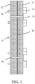
- the antenna array coupling and calibrating network includes a dielectric plate 31, a coupling and calibrating network 32, an antenna array, 16 first radio frequency connectors 36 and one second radio frequency connector 37, herein, the antenna array and the coupling and calibrating network 32 are provided on the front and back sides of the dielectric plate 31, respectively, and an intermediate layer of the dielectric plate 31 serves as a ground layer and a metallic reflection plate 34 simultaneously, the dielectric plate 31 is provided with a via hole 38 through which the antenna array is connected to the coupling and calibrating network 32.
- the dielectric plate 31 is a printed circuit board (PCB), one side is provided with the antenna array, one side is printed with the coupling and calibrating network 32; the intermediate layer of the dielectric plate 31 serves as the ground layer of the coupling and calibrating network 32 and the antenna array, as well as the metallic reflection plate 34 of the antenna array, to enhance the directional radiation of the antenna array.
- PCB printed circuit board
- the antenna array consists of 16 antenna array elements 33 for receiving or transmitting signals, which may be in a linear arrangement, an annular arrangement or other irregular shaped arrangements; and/or the 16 antenna array elements 33 may also be arranged at equal spacing, or arranged at unequal spacing; and/or the 16 antenna array elements 33 may also be directional, unipolar or dual polarized; and/or the 16 antenna array elements 33 may be directional at any angle, such as 30 °, 60 °, and the like; and/or the dual-polarization of the 16 antenna array elements 33 may be horizontal and vertical polarization, or ⁇ 45 ° polarization.
- the coupling and calibrating network 32 includes a microstrip directional coupler and a shunt/combiner, the number of microstrip directional couplers is the same as the number of antenna array elements, and the microstrip directional couplers correspond to the antenna array elements one by one, and after realizing shunt feed by way of the microstrip line 35 and the like, each antenna element 33 is connected, through the via hole 38, to a corresponding microstrip directional coupler on the coupling and calibrating network 32, thus the antenna array and the coupling calibration network can be provided on the same dielectric plate, and cable welding way which is harmful to production is prevented.
- the downstream calibration working link flow of the abovementioned device is that the 16 radio frequency signals of the base station system transmission channel are input by 16 first radio frequency connectors 36, respectively, and output to a calibration link of the base station system through the second radio frequency connector 37 for calibrating after coupling via the coupling and calibrating network 32 and combining into one calibration signal by way of "constant differential loss, constant phase shift".
- the upstream calibration working link flow of the abovementioned device is that a calibration signal from the base station system calibration link is input through the second radio frequency connector 37, divided into 16 signals via the coupling and calibrating network 32 by way of "constant differential loss, constant phase shift", and after coupling, output to the receiving channel of the base station system by the 16 first radio frequency connectors 36, respectively.
- the 16 first radio frequency connectors 36 and the second RF connector 37 are arranged inside the dielectric plate 31 (or mounted on the dielectric plate), non-edge extension area, which facilitates miniaturization and integration of the structure, any other reliable connection modes of similar functions can be used, not repetitively described.
- the first radio frequency connector 36 is used to input or output the radio frequency signal
- the second radio frequency connector 37 is used to input or output the calibration signal
- the radio frequency connector with blind insertion, radial and axial floating characteristics may be used to facilitate connection with the base station system.
- Each antenna array element 33 of each column of the antenna array elements has a polarization direction of + 45° and -45° in the vertical direction or in the horizontal direction to transmit and receive signal; two adjacent antenna array elements 33, in the up-down direction, of each column of the antenna array elements employ the microstrip line 35 and so on to achieve the shunt feed, connect to the microstrip directional coupler through the via hole 38.
- each antenna array element may be distributed and arranged, not only in parallel, equidistant distribution, but also in staggered, unequal spacing distribution, or in different combinations of these modes.
- the antenna array element 33 may be a metallic oscillator, or in a form of a microstrip structure or a patch structure, the antenna array element 33 may be in a dual polarization mode or in a single polarization mode.
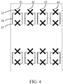
- longitudinal metallic baffles 51, 52, 53 may be provided vertically between the two adjacent columns of antenna array elements 41 and 42, 42 and 43, and 43 and 44, respectively, the metallic baffles 51, 52, 53 are electrically connected or capacitively coupled with the metal reflector 34.
- baffles may be further provided around, that is, the metallic baffles 54, 55, 56, which intersect perpendicularly with the metallic baffles 51, 52, and 53, may be added, and at the same time, metallic side plates 57, 58, 59, 60 may be provided surrounding the antenna array elements, the way for adding the metallic baffles and the surrounding side plates is not limited to the way shown in Fig. 5 , and the metallic baffles may be designed separately or may be integrated on an antenna housing structure to improve the strength of the antenna housing and enhance the antenna system security and stability. By other ways such as adding a small cover above the antenna array element, etc., each antenna array element may have a more independent space, which would not be repetitively described.
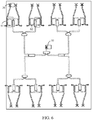
- the coupling and calibrating network includes 16 identical microstrip directional coupling circuits 61, 15 1: 2 power shunt/combiners 62, 16 first radio frequency connectors 36, one second radio frequency connector 37 for calibrating the input and output of the signal.
- every two adjacent microstrip directional coupling circuits 61 are connected through a 1: 2 power shunt/combiner 62, one end of each microstrip directional coupling circuit 61 is connected to a first radio frequency connector 36 and the other end is connected to an adjacent microstrip directional coupling circuit through a 1: 2 power shunt/combiner 62.
- Two shunt ports of each 1: 2 power shunt/combiner 62 are connected to two microstrip directional coupling circuits 61, respectively, 15 1: 2 power shunt/combiners are connected to the second radio frequency connector 37 after the combiner ports of the 15 1: 2 power shunt/combiners are connected.
- the number of 16 microstrip directional couplers is equal to the number of the antenna array elements, by using two similar metallic parallel microstrip lines, an excellent product performance consistency is obtained.
- the 16 microstrip directional coupling circuits 61 are distributed with 16 antenna array elements on a circuit board of the coupling and calibrating network correspondingly, and each microstrip directional coupler is connected to a first radio frequency connector to facilitate communication with the radio frequency transceiver of the base station system, and the 16 microstrip directional couplers are identical and easy to product and debug, the 16 microstrip directional couplers are electrically connected with the corresponding antenna elements by the via hole, which has a better performance to ensure consistency between amplitude and phase of the signal from the microstrip directional coupler to the oscillator of the antenna, while the structure is simply integrated, highly reliable and ease for producing.
- the number of power shunt/combiner 62 is limited by the number of shunt/combination-channels, and the embodiment of Figure 6 employs a 1: 2 power shunt/combiner, requiring 15 power shunt/combiners 62 to achieve the shunt/combination of the16-way signal, finally a signal is composed to the second radio frequency connector 37. If a 1: 4 power shunt/combiner is employed, only 5 1: 4 power shunt/combiners are required to achieve the shunt/combination of the 16 signals after the 16 antenna array elements and 16 microstrip directional couplers are provided.
- FIG. 7 is a schematic diagram of any one of the coupling units in the coupling and calibrating network of an embodiment of the present invention, herein, a coupling unit includes two microstrip directional couplers 61 and a 1: 2 power shunt/combiner, each microstrip directional coupler 61 includes two microstrips, one end of a microstrip 71 is connected to an antenna element 33 via the via hole 38, and the other end is connected to the radio frequency input of the radio frequency transceiver corresponding to the base station system, i.e., connected to the first radio frequency connector 36; one end of another microstrip 72 is connected to a matched load 74 of 50 ⁇ (also grounded) and the other end is connected to a shunt port of the 1: 2 power shunt/combiner 62.
- the reference number 73 in Figure 7 is the isolation resistor of the power shunt/combiner 62.
- the abovementioned embodiment is the coupling and calibrating network device of the antenna array of 16 array elements, and a coupling and calibrating network device of a larger-scale antenna array, such as of 32, 64, 128 array elements, can be designed according to the same principle.
- the embodiment of the present invention is particularly applicable to a large scale antenna array.
- an antenna array, a coupling and calibrating network and a metal reflection plate are all integrated into a same dielectric plate, and an antenna array elements and the coupling and calibrating network are connected by a via hole to increase the reliability and avoid the use of a large number of radio frequency cables, which may reduce the size of an antenna, improve integration and miniaturization performances of the base station system, it is beneficial to realization of the coupling and calibrating network device of large-scale intelligent antenna array, convenient for producing and debugging and large-scale production, more suitable for the popularization and development of wireless communication systems.
Landscapes
- Variable-Direction Aerials And Aerial Arrays (AREA)
- Transceivers (AREA)
Applications Claiming Priority (2)
| Application Number | Priority Date | Filing Date | Title |
|---|---|---|---|
| CN201420630111.6U CN204243214U (zh) | 2014-10-28 | 2014-10-28 | 一种智能天线装置 |
| PCT/CN2015/076648 WO2016065859A1 (fr) | 2014-10-28 | 2015-04-15 | Dispositif d'antenne intelligent |
Publications (2)
| Publication Number | Publication Date |
|---|---|
| EP3214700A1 true EP3214700A1 (fr) | 2017-09-06 |
| EP3214700A4 EP3214700A4 (fr) | 2017-11-01 |
Family
ID=52772665
Family Applications (1)
| Application Number | Title | Priority Date | Filing Date |
|---|---|---|---|
| EP15854044.3A Withdrawn EP3214700A4 (fr) | 2014-10-28 | 2015-04-15 | Dispositif d'antenne intelligent |
Country Status (4)
| Country | Link |
|---|---|
| EP (1) | EP3214700A4 (fr) |
| JP (1) | JP2017539134A (fr) |
| CN (1) | CN204243214U (fr) |
| WO (1) | WO2016065859A1 (fr) |
Cited By (1)
| Publication number | Priority date | Publication date | Assignee | Title |
|---|---|---|---|---|
| WO2019209903A1 (fr) * | 2018-04-27 | 2019-10-31 | Commscope Technologies Llc | Circuits d'étalonnage pour antennes de formation de faisceau, et antennes de station de base associées |
Families Citing this family (16)
| Publication number | Priority date | Publication date | Assignee | Title |
|---|---|---|---|---|
| CN105634627B (zh) * | 2014-10-28 | 2021-04-02 | 中兴通讯股份有限公司 | 一种天线阵耦合校准网络装置及校准方法 |
| CN204243214U (zh) * | 2014-10-28 | 2015-04-01 | 中兴通讯股份有限公司 | 一种智能天线装置 |
| CN105790860B (zh) * | 2014-12-25 | 2020-12-29 | 中兴通讯股份有限公司 | 天线耦合校准系统 |
| CN105390814B (zh) * | 2015-10-18 | 2018-06-26 | 中国电子科技集团公司第十研究所 | 具有内校准网络的有源相控阵天线 |
| CN107402371A (zh) * | 2016-05-20 | 2017-11-28 | 国家海洋技术中心 | 一种智能天线阵 |
| CN106099394B (zh) * | 2016-06-28 | 2019-01-29 | 武汉虹信通信技术有限责任公司 | 一种用于5g系统的密集阵列天线 |
| CN110416706B (zh) * | 2018-04-27 | 2023-07-11 | 康普技术有限责任公司 | 用于波束成形天线和相关基站天线的校准电路 |
| CN108808224B (zh) * | 2018-06-29 | 2020-12-15 | 京信通信技术(广州)有限公司 | Massive mimo天线 |
| CN109005603A (zh) * | 2018-09-11 | 2018-12-14 | 雷士(北京)光电工程技术有限公司 | 一体化照明装置 |
| CN109994820B (zh) * | 2019-03-28 | 2024-01-30 | 中天宽带技术有限公司 | 一种大规模mimo天线 |
| WO2021000261A1 (fr) * | 2019-07-02 | 2021-01-07 | 瑞声声学科技(深圳)有限公司 | Substrat d'antenne et procédé de fabrication de substrat d'antenne |
| CN112242612B (zh) | 2019-07-19 | 2025-05-23 | 户外无线网络有限公司 | 贴片天线 |
| CN112397863B (zh) * | 2019-08-16 | 2022-02-22 | 稜研科技股份有限公司 | 用于毫米波的转接结构以及多层转接结构 |
| WO2021128327A1 (fr) * | 2019-12-27 | 2021-07-01 | 瑞声声学科技(深圳)有限公司 | Antenne de station de base |
| EP4343966A4 (fr) | 2021-10-08 | 2024-10-30 | Samsung Electronics Co., Ltd. | Structure d'antenne et dispositif électronique la comprenant |
| CN115913410A (zh) * | 2022-10-17 | 2023-04-04 | 华南理工大学 | 用于多通道天线阵列馈电网络的宽带校准网络 |
Family Cites Families (14)
| Publication number | Priority date | Publication date | Assignee | Title |
|---|---|---|---|---|
| US5412414A (en) * | 1988-04-08 | 1995-05-02 | Martin Marietta Corporation | Self monitoring/calibrating phased array radar and an interchangeable, adjustable transmit/receive sub-assembly |
| JP3185406B2 (ja) * | 1992-10-13 | 2001-07-09 | 日立化成工業株式会社 | 平面アンテナ |
| DE19806914C2 (de) * | 1998-02-19 | 2002-01-31 | Bosch Gmbh Robert | Verfahren und Vorrichtung zum Kalibrieren einer Gruppenantenne |
| JP2002043832A (ja) * | 2000-07-21 | 2002-02-08 | Tdk Corp | 円偏波パッチアンテナ |
| CN1157966C (zh) * | 2001-07-20 | 2004-07-14 | 电信科学技术研究院 | 无线通信系统智能天线阵的耦合校准网络及耦合校准方法 |
| US20030227420A1 (en) * | 2002-06-05 | 2003-12-11 | Andrew Corporation | Integrated aperture and calibration feed for adaptive beamforming systems |
| US7127255B2 (en) * | 2002-10-01 | 2006-10-24 | Trango Systems, Inc. | Wireless point to multipoint system |
| US20040063438A1 (en) * | 2002-10-01 | 2004-04-01 | Hsu Yun-Hsiang Kenny | Wireless point to multipoint system |
| JP4118835B2 (ja) * | 2004-05-25 | 2008-07-16 | 日本電波工業株式会社 | 機能平面アレーアンテナ |
| CN2755871Y (zh) * | 2004-11-17 | 2006-02-01 | 大唐移动通信设备有限公司 | 直线排列智能天线阵的耦合校准网络装置 |
| CN201134510Y (zh) * | 2007-10-31 | 2008-10-15 | 京信通信系统(中国)有限公司 | 小型化智能天线系统 |
| JP5596857B2 (ja) * | 2010-07-01 | 2014-09-24 | ノキア シーメンス ネットワークス オサケユキチュア | アンテナ構成体 |
| JPWO2014083948A1 (ja) * | 2012-11-27 | 2017-01-05 | 国立大学法人佐賀大学 | アンテナ装置 |
| CN204243214U (zh) * | 2014-10-28 | 2015-04-01 | 中兴通讯股份有限公司 | 一种智能天线装置 |
-
2014
- 2014-10-28 CN CN201420630111.6U patent/CN204243214U/zh not_active Expired - Lifetime
-
2015
- 2015-04-15 JP JP2017523399A patent/JP2017539134A/ja active Pending
- 2015-04-15 EP EP15854044.3A patent/EP3214700A4/fr not_active Withdrawn
- 2015-04-15 WO PCT/CN2015/076648 patent/WO2016065859A1/fr not_active Ceased
Cited By (4)
| Publication number | Priority date | Publication date | Assignee | Title |
|---|---|---|---|---|
| WO2019209903A1 (fr) * | 2018-04-27 | 2019-10-31 | Commscope Technologies Llc | Circuits d'étalonnage pour antennes de formation de faisceau, et antennes de station de base associées |
| US20190334636A1 (en) * | 2018-04-27 | 2019-10-31 | Commscope Technologies Llc | Calibration circuits for beam-forming antennas and related base station antennas |
| US10812200B2 (en) * | 2018-04-27 | 2020-10-20 | Commscope Technologies Llc | Calibration circuits for beam-forming antennas and related base station antennas |
| US11411661B2 (en) * | 2018-04-27 | 2022-08-09 | Commscope Technologies Llc | Calibration circuits for beam-forming antennas and related base station antennas |
Also Published As
| Publication number | Publication date |
|---|---|
| JP2017539134A (ja) | 2017-12-28 |
| EP3214700A4 (fr) | 2017-11-01 |
| WO2016065859A1 (fr) | 2016-05-06 |
| CN204243214U (zh) | 2015-04-01 |
Similar Documents
| Publication | Publication Date | Title |
|---|---|---|
| EP3214700A1 (fr) | Dispositif d'antenne intelligent | |
| US12160031B2 (en) | Feed network of base station antenna, base station antenna, and base station | |
| CN105634627B (zh) | 一种天线阵耦合校准网络装置及校准方法 | |
| CN105790860B (zh) | 天线耦合校准系统 | |
| CN110828976B (zh) | 天线系统和基站 | |
| US11205836B2 (en) | Base station antenna and antenna array module thereof | |
| AU2008305785B2 (en) | Antenna arrangement for a multi radiator base station antenna | |
| CN107799896A (zh) | 一种运用于3500MHz附近频段的TD‑LTE智能天线 | |
| CN105305073B (zh) | 多入多出天线结构及移动终端 | |
| CN112332114B (zh) | 一种用于无线定位系统的微带阵列天线 | |
| CN111430941A (zh) | 一种用于5g通信的智能拼接天线 | |
| CN110797654A (zh) | 一种同频带间高隔离度天线及微基站 | |
| CN210040568U (zh) | 单层同轴馈电双极化微带阵列天线 | |
| US12418107B2 (en) | Systems and methods for generating calibration data in active antenna modules having antenna-side filter arrays therein | |
| CN210984950U (zh) | 一种同频带间高隔离度天线及微基站 | |
| CN211045721U (zh) | 天线和天线阵列 | |
| CN205016679U (zh) | 双频模块天线及其电子设备 | |
| CN104143692B (zh) | 多天线阵列和基站 | |
| CN102760971B (zh) | 一种双频高增益载波速双极化天线 | |
| CN103730719B (zh) | 一种基于印刷电路板的小尺寸高隔离三单元多输入多输出天线 | |
| CN209329172U (zh) | 基站天线及通信基站系统 | |
| CN117525860A (zh) | 一种新型双卫星系统天线 | |
| CN112397899A (zh) | 一种5g阵列天线 |
Legal Events
| Date | Code | Title | Description |
|---|---|---|---|
| PUAI | Public reference made under article 153(3) epc to a published international application that has entered the european phase |
Free format text: ORIGINAL CODE: 0009012 |
|
| 17P | Request for examination filed |
Effective date: 20170525 |
|
| AK | Designated contracting states |
Kind code of ref document: A1 Designated state(s): AL AT BE BG CH CY CZ DE DK EE ES FI FR GB GR HR HU IE IS IT LI LT LU LV MC MK MT NL NO PL PT RO RS SE SI SK SM TR |
|
| AX | Request for extension of the european patent |
Extension state: BA ME |
|
| A4 | Supplementary search report drawn up and despatched |
Effective date: 20170928 |
|
| RIC1 | Information provided on ipc code assigned before grant |
Ipc: H04B 17/14 20150101ALI20170922BHEP Ipc: H01Q 21/00 20060101ALI20170922BHEP Ipc: H01Q 3/26 20060101AFI20170922BHEP |
|
| DAV | Request for validation of the european patent (deleted) | ||
| DAX | Request for extension of the european patent (deleted) | ||
| STAA | Information on the status of an ep patent application or granted ep patent |
Free format text: STATUS: THE APPLICATION IS DEEMED TO BE WITHDRAWN |
|
| 18D | Application deemed to be withdrawn |
Effective date: 20180501 |