EP3214905B1 - Dispositif semi-conducteur, dispositif de commande de source de lumière et système de commande de source de lumière - Google Patents
Dispositif semi-conducteur, dispositif de commande de source de lumière et système de commande de source de lumière Download PDFInfo
- Publication number
- EP3214905B1 EP3214905B1 EP17157899.0A EP17157899A EP3214905B1 EP 3214905 B1 EP3214905 B1 EP 3214905B1 EP 17157899 A EP17157899 A EP 17157899A EP 3214905 B1 EP3214905 B1 EP 3214905B1
- Authority
- EP
- European Patent Office
- Prior art keywords
- data
- light source
- level
- deterioration
- waveform
- Prior art date
- Legal status (The legal status is an assumption and is not a legal conclusion. Google has not performed a legal analysis and makes no representation as to the accuracy of the status listed.)
- Active
Links
Images












Classifications
-
- H—ELECTRICITY
- H05—ELECTRIC TECHNIQUES NOT OTHERWISE PROVIDED FOR
- H05B—ELECTRIC HEATING; ELECTRIC LIGHT SOURCES NOT OTHERWISE PROVIDED FOR; CIRCUIT ARRANGEMENTS FOR ELECTRIC LIGHT SOURCES, IN GENERAL
- H05B47/00—Circuit arrangements for operating light sources in general, i.e. where the type of light source is not relevant
- H05B47/10—Controlling the light source
-
- H—ELECTRICITY
- H04—ELECTRIC COMMUNICATION TECHNIQUE
- H04L—TRANSMISSION OF DIGITAL INFORMATION, e.g. TELEGRAPHIC COMMUNICATION
- H04L1/00—Arrangements for detecting or preventing errors in the information received
- H04L1/20—Arrangements for detecting or preventing errors in the information received using signal quality detector
- H04L1/205—Arrangements for detecting or preventing errors in the information received using signal quality detector jitter monitoring
-
- G—PHYSICS
- G01—MEASURING; TESTING
- G01R—MEASURING ELECTRIC VARIABLES; MEASURING MAGNETIC VARIABLES
- G01R29/00—Arrangements for measuring or indicating electric quantities not covered by groups G01R19/00 - G01R27/00
- G01R29/02—Measuring characteristics of individual pulses, e.g. deviation from pulse flatness, rise time or duration
- G01R29/027—Indicating that a pulse characteristic is either above or below a predetermined value or within or beyond a predetermined range of values
-
- H—ELECTRICITY
- H05—ELECTRIC TECHNIQUES NOT OTHERWISE PROVIDED FOR
- H05B—ELECTRIC HEATING; ELECTRIC LIGHT SOURCES NOT OTHERWISE PROVIDED FOR; CIRCUIT ARRANGEMENTS FOR ELECTRIC LIGHT SOURCES, IN GENERAL
- H05B47/00—Circuit arrangements for operating light sources in general, i.e. where the type of light source is not relevant
- H05B47/10—Controlling the light source
- H05B47/175—Controlling the light source by remote control
- H05B47/18—Controlling the light source by remote control via data-bus transmission
- H05B47/183—Controlling the light source by remote control via data-bus transmission using digital addressable lighting interface [DALI] communication protocols
-
- H—ELECTRICITY
- H05—ELECTRIC TECHNIQUES NOT OTHERWISE PROVIDED FOR
- H05B—ELECTRIC HEATING; ELECTRIC LIGHT SOURCES NOT OTHERWISE PROVIDED FOR; CIRCUIT ARRANGEMENTS FOR ELECTRIC LIGHT SOURCES, IN GENERAL
- H05B47/00—Circuit arrangements for operating light sources in general, i.e. where the type of light source is not relevant
- H05B47/20—Responsive to malfunctions or to light source life; for protection
Definitions
- the present disclosure relates to a device that adjusts lighting of illumination equipment.
- an illumination control system a system that controls illumination equipment (illumination control system) by transmitting a signal complying with Digital Addressable Lighting Interface (DALI) standards, as a light adjustment command signal, is developed.
- DALI Digital Addressable Lighting Interface
- an illumination control system complying with DALI standards is proposed in Japanese Unexamined Patent Application Publication No. 2013-4484
- Patent Document 2 A semiconductor device according to the preamble of claim 1 is disclosed in Patent Document 2.
- the present disclosure has been developed to solve the above problem and is intended to provide a semiconductor device, a light source control device, and a light source control system capable of diagnosing communication network quality.
- the invention resides in a light source control system comprising a server and a semiconductor device as defined in claim 1 that is to be coupled to a light source.
- the deterioration detector detects deterioration of an interface module, it is possible to check and diagnose communication network quality. It is also possible to extend the lifetime of a communication network.
- Fig. 1 is a diagram to explain a configuration of a light source control system 1 according to a first embodiment.
- the light source control system 1 includes multiple light source blocks 100 and a server 2.
- the server 2 is coupled to multiple light source blocks 100 via a bus BS2.
- Each light source block 100 is controlled by transmitting and receiving a signal complying with DALI standards via a bus BS1.
- Each light source block 100 includes multiple light sources 3 and multiple controllers 10, each of which is provided to control each of the light sources 3.
- each light source block 100 further includes multiple communication interface modules 5 which are provided respectively for each of the controllers 10, each module being provided between the bus BS2 and a controller 10 to which it couples, and multiple DALI communication interface modules 4, each module being provided between the bus BS1 and a controller 10 to which it couples. And now, it is not necessary to allocate one communication interface module 5 to one controller 10. It is assumed that the bus BS1 and the bus BS2 comply with different communication standards.
- the DALI communication interface modules 4 are provided such that they can send and receive data to/from one another via the bus BS2.
- Each controller 10 controls a light source 3, based on a command signal to turn the light source 3 on or off which is received via one of the DALI communication interface modules 4.
- each controller 10 transmits information to the server 2 coupled to the bus BS2 via one of the communication interface modules 5.
- the server 2 is provided such that it can communicate with each controller 10 via the bus BS2.
- N + 1 light sources 3 are provided is illustrated by way of example.
- a 0-th light source 3 is denoted as a light source 3-0. This way also applies to other elements; controllers 10, DALI communication interface modules 4, and communication interface modules 5.
- Fig. 2 is a diagram to explain a configuration of a controller 10 and its peripheral circuit according to the first embodiment.
- the controller 10 which is a semiconductor device is coupled to a light source 3, a DALI communication interface module 4, and a communication interface module 5.
- the DALI communication interface module 4 is provided to enable communication with another controller 10 which is another semiconductor device by a signal complying with DALI communication standards via the bus BS1.
- the communication interface module 5 is provided to enable communication with the server 2 using communication standards, for example, Ethernet (a registered trademark) different from the DALI communication standards via the bus BS2.
- a wireless coupling method can also be adopted, not limited to wired coupling.
- the controller 10 includes a driving circuit block 11, a signal processing unit 12, and a deterioration detector 13.
- the driving circuit block 11 may be located outside the controller 10 in some cases.
- the driving circuit block 11 drives the light source 3.
- the signal processing unit 12 processes a signal received via the DALI communication interface module 4 and gives a command to the driving circuit block 11.
- the driving circuit block 11 executes light adjustment control such as turning the light source 3 off or on, according to a command from the signal processing unit 12.
- the deterioration detector 13 is coupled to the signal processing unit 12 and detects a condition of a signal received via the DALI communication interface module 4.
- the signal processing unit 12 is coupled to the communication interface module 5 and transmits data to the server 2 as necessary. And now, a controller 10 that is not coupled to a communication interface module 5 once transmits data to a controller 10 coupled to a communication interface module 5 and, subsequently, the data is transferred to the server 2 via the bus BS2.
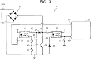
- Fig. 3 is a diagram to explain a configuration of a DALI communication interface module 4 according to the first embodiment.
- the DALI communication interface module 4 includes a diode bridge 20, photo couplers 21, 22, resistors 23, 24, 25, 28, 29, 31, a capacitor 26, a diode 27, a zener diode 30, and a bipolar transistor 32.
- the diode bridge 20 is coupled to the bus BS1 which is comprised of two lines and nodes N0 and N2.
- a transmit pin TP of the controller 10 is coupled to a photo coupler 21 via a resistor 23.
- the photo coupler 21 includes a light emitting diode and a photo transistor. The light emitting diode is provided between a power supply voltage and the resistor 23.
- One end terminal of the photo transistor is coupled to a node N3. Its other end terminal is coupled to a node N1 via a resistor 24.
- a resistor 25 is coupled between the node N2 and the node N1.
- a resistor 28 and the bipolar transistor 32 are serially coupled between the node N0 and the node N2.
- a gate electrode of the bipolar transistor 32 is coupled to the node N1.
- a diode is provided between the node N3 and the node N0.
- the capacitor 26 is coupled between the node N3 and the node N2.
- the node N0 is coupled to a photo coupler 22 via a resistor 29.
- the photo coupler 22 includes a light emitting diode and a photo transistor.
- An anode terminal of the light emitting diode is coupled to the resistor 29. Its cathode terminal is coupled to the zener diode 30.
- One end terminal of the photo coupler 22 is coupled to a power supply voltage. Its other end terminal is coupled to a receive pin RP of the controller 10.
- a resistor 31 is coupled between the receive pin RP and a ground voltage.
- the photo couplers 21, 22 of the DALI communication interface module 4 diagnose deterioration.
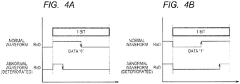
- Figs. 4A and 4B are diagrams to explain a 1-bit data waveform according to the first embodiment.
- communication data complying with DALI standards is assumed to be Manchester encoded.
- a data waveform for data "0" is illustrated here.
- a data waveform that falls from "H” level to "L” level substantially at a middle point of a cyclic period assigned to one bit is illustrated.
- a signal is taken as data "0” by detecting a falling edge (change timing) from "H" level to "L” level.
- a data waveform that falls from “H” level to "L” level during the early part of a cyclic period assigned to one bit is illustrated.
- a data waveform for data "1" is illustrated here.
- a data waveform that rises from “L” level to "H” level substantially at a middle point of a cyclic period assigned to one bit is illustrated.
- a signal is taken as data “1” by detecting a rising edge (change timing) from "L level to "H” level.
- FIG. 4A and 4B illustrate a case where "L" level in an abnormal waveform continues longer than that in a normal waveform. There may occur a case where "H” level in an abnormal waveform continues longer than that in a normal waveform (illustration omitted).
- Such an abnormal waveform is attributed to aging deterioration of the photo couple 21 provided in the transmitting side and the photo coupler 22 provided in the receiving side, as an example, and results in a decrease in communication quality.
- Figs. 5A and 5B are diagrams to explain a method of judging whether a 1-bit data waveform deteriorates according to the first embodiment.
- a window width a predetermined interval for data detection is set.
- Interval T0 is set as an initial value.
- the window width is adjustable by T0 + m ⁇ ⁇ T (m: a positive integer) .
- T0 m ⁇ ⁇ T
- a window width a predetermined interval for data detection is set. Interval T0 is set as an initial value. The window width is adjustable by T0 + m ⁇ ⁇ T (m: a positive integer) . With reference to a starting point (right-hand) from which interval T0O was set, the window width becomes wider to the left, as m increases.
- Figs. 6A and 6B are diagrams to explain another method of judging whether a 1-bit data waveform deteriorates according to the first embodiment. Referring to Fig. 6A , in the present example, an instance of judging whether a data waveform for data "1" deteriorates is illustrated.
- a window width a predetermined interval for data detection is set. Interval T0 is set as an initial value.
- the window width is adjustable by T0 + m ⁇ ⁇ T (m: a positive integer) .
- T0 m + m ⁇ ⁇ T
- the window width becomes wider to the left, as m increases. That is, the interval for data detection becomes longer. Therefore, a judgment can be made such that, if m is smaller (the window width is narrower), the data waveform deteriorates to a small extent; if m is larger (the window width is wider), the data waveform deteriorates to a large extent.
- Fig. 6B an instance of judging whether a data waveform for data "0" deteriorates is illustrated.
- a window width a predetermined interval for data detection is set.
- Interval T0 is set as an initial value.
- the window width is adjustable by T0 + m ⁇ ⁇ T (m: a positive integer) .
- the window width With reference to a starting point (left-hand) from which interval T0 was set, the window width becomes wider to the right, as m increases. That is, the interval for data detection becomes longer. Therefore, a judgment can be made such that, if m is smaller (the window width is narrower), the data waveform deteriorates to a small extent; if m is larger (the window width is wider), the data waveform deteriorates to a large extent.
- Fig. 7 is a flowchart by which judging whether data deteriorates is executed according to the first embodiment. This process is processing by the deterioration detector 13 within the controller 10.
- the controller 10 performs a receiving operation (step S6) .
- the controller 10 judges whether all edges of received data are falling within the timing window (step S8). And now, as received data, received data for test use (such as all 0s or 1s) can be used. If it has been judged at step S8 that all edges of received data are falling within the timing window (Yes at step S8), the timing window setting value is stored (step S10).
- the process terminates (END). Otherwise, if it has been judged at step S8 that all edges of received data are not falling within the timing window (No at step S8), the variable n is incremented (step S12). And, the process returns to step S4. This process is repeated until all edges of received data fall within the timing window.
- the deterioration detector 13 can diagnose communication quality attributed to aging deterioration of the photo couplers 21 and 22. That is, the deterioration detector 13 judges whether or not all edges of received data fall within the set timing window and judges that communication quality deteriorates, if the edges do not fall within the timing window. Then, an adjustment is made of the timing window. According to an adjustment level, a degree of how communication quality deteriorates can be judged.
- Fig. 8 is a diagram to explain one example of a score table for use in the light source control system 1 according to the second embodiment.
- a score table is divided into a transmitting side and a receiving side.
- 0-th to N-th DALI communication interface modules 4 are listed in a vertical direction.
- a signal transmitted through a 0-th DALI communication interface module 4 can be received by the 0-th DALI communication interface module.
- data transmitted through the 0-th DALI communication interface module 4 is transmitted via the bus BS1.
- 0-th to N-th DALI communication interface modules 4 receive the data transmitted through the 0-th DALI communication interface module 4.
- Score values of the width of a timing window upon receiving the data are presented. As one example, when data has been transmitted through the 0-th DALI communication interface module 4-0, score values corresponding to the timing window widths upon receiving the data through the 0-th to N-th DALI communication interface modules 4-0 to 4-N are presented as T00, T01, ..., T0n.
- the server 2 collects information and creates this score table.
- the deterioration detector 13 within the controller 10 sets a timing window according to the method described for the first embodiment and acquires a value of "m" as a score value when having set the timing window.
- the signal processing unit 12 within the controller 10 transmits the value of "m" acquired upon having set the timing window to the server 2 via the communication interface module 5.
- the server 2 collects score values m from the respective controllers 10 and creates a score table.
- Figs. 9A to 9D are diagrams to explain transition of the score table according to the second embodiment. Referring to Fig. 9A , an instance where all score values "m" are 1 is illustrated. Subsequently, as in Figs. 9B to 9D , illustrated are instances where communication quality deteriorates with score values changing, as components of the DALI communication interface modules 4 deteriorate.
- Fig. 10 is a diagram to explain a method of diagnosing a degree of deterioration based on the score table of the second embodiment. Referring to Fig. 10 , the same score table as the score table in Fig. 9D is illustrated.
- the maximum values are "4", "5", ... "6". Then, a judgment is made of whether or not each maximum value is more than a predetermined threshold. For example, "5" is assumed to be set as the threshold. Then, it is judged that DALI communication interface modules 4 for which a score value is more than "5" should be repaired or replaced. In the present example, it is judged that the first and N-th DALI communication interface modules 4 should be repaired or replaced. Based on such analysis, it is enabled to diagnose a degree of how communication quality deteriorates across the light source control system 1. Thus, by identifying a DALI communication interface module 4 which needs to be repaired or replaced and performing a predefined work procedure, it would become possible to maintain communication network quality.
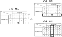
- Figs. 11A to 11C are diagrams to explain a method of diagnosing a degree of deterioration based on a score table which is a first modification example of the second embodiment.
- minimum values in every row are picked out here.
- the minimum values are "1", "2", ... "3".
- the score table is divided into two tables.
- Fig. 11B is a score table reflecting the minimum values.
- Fig. 11C illustrates a table of score values which are differentials between the values in the score table of Fig. 11B and the values in the score table of Fig. 11A . By calculating a table of score values which are such differentials, it is enabled to identify deterioration of communication quality in a particular place.
- a method of diagnosing communication network quality using score values of timing window width was described, but no limitation to this is intended. It is also possible to diagnose communication network quality by, for example, counting an "L" level period or "H” level period.
- Figs. 12A and 12B are diagrams to explain a method of judging whether a data waveform deteriorates according to a second modification example of the second embodiment.
- a data waveform for data "1" is illustrated.
- a data waveform for data "0" is illustrated.
- an "L" level period is longer than a reference value and its count value is large, it may be judged that communication quality decreases.
- an "H" level period is longer than a reference value and its count value is large, it may be judged that communication quality decreases.
- an instance where such period is longer was described, it may also be judged that communication quality decreases, if such period is shorter.
- Fig. 13 is a diagram to explain a controller 10A according to the third embodiment.
- the controller 10A includes a signal processing unit 12A.
- the signal processing unit 12A includes a transmitter 16, an adjuster 15, and a receiver 17.
- the transmitter 16 transmits data to the bus BS1 through a DALI communication interface module 4.
- the receiver 17 receives data from the bus BS1 through a DALI communication interface module 4.
- the adjuster 15 adjusts an "L" level period of data to transmit from the transmitter 16 to the DALI communication interface module 4.
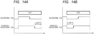
- Figs. 14A and 14B are diagrams to explain adjusting the waveform of a data signal to transmit from the transmitter 16 according to the third embodiment.
- Fig. 14A an instance of executing a waveform adjustment for a data signal representing data "0" is illustrated here.
- the adjuster 15 executes a waveform adjustment to shorten an "L" level period from a reference value (initial value).
- Fig. 14B an instance of executing a waveform adjustment for a data signal representing data "1” is illustrated here.
- the adjuster 15 executes a waveform adjustment to shorten an "L" level period from a reference value (initial value).
- Fig. 15 is a flowchart to explain a waveform adjustment process according to the third embodiment. Referring to Fig. 15 , processing by the adjuster 15 is mainly described here.
- Fig. 16 is a flowchart to explain processing by the server 2 according to the third embodiment. Referring to Fig. 15 , the server 2 checks the score table (step S12). In particular, the server checks the score table as described with Fig. 10 . Next, the server 2 specifies a module for which an adjustment is required (step S14).
- the server 2 specifies a DALI communication interface module 4 for which a score value is more than a predetermined threshold, as described with Fig. 10 .
- a DALI communication interface module 4 for which a score value is more than a predetermined threshold, as described with Fig. 10 .
- the server 2 gives an adjustment command (step S16).
- the server 2 outputs a command to make a waveform adjustment to the first controller 10-1 via the bus BS2.
- the adjuster 15 within the controller 10-1 executes an adjustment to shorten an "L" level period of transmission data.
- the server 2 gives a command to transmit a signal (step S18).
- the server 2 outputs a command to output a transmission signal for test use to the first controller 10-1 via the bus BS2.
- the controller 10-1 transmits transmission data in which the "L" level period made shorter.
- the server 2 acquires score values (step S20).
- the respective controllers 10 which have received transmission data from the controller 10-1 perform a deterioration judgment for the data, as described previously.
- the controllers 10 output a score value m resulting from the judgment to the server 2.
- the server 2 acquires score values transmitted from the respective controllers 10.
- the server 2 judges whether or not the score values are more than a threshold (step S22). In particular, the server 2 judges whether or not the score values acquired from the respective controllers are more than, e.g., a threshold of "5".
- step S22 the server 2 has judged that the acquired score values (if any) are more than a threshold (YES at step S22), the process returns to step S16 and the server 2 further outputs an adjustment command.
- the server 2 outputs a command to make a waveform adjustment to the first controller 10-1 via the bus BS2. Accordingly, the adjuster 15 within the controller 10-1 executes an adjustment to shorten an "L" level period of a transmission data.
- the server 2 If, at step S22, the server 2 has judged that the score values are less than a threshold (NO at step S22), it terminates the process. In particular, if the score values acquired from the respective server are less than, e.g., a threshold of "5", the server 2 terminates the process.
- a threshold of "5" e.g., a threshold of "5"
- the server 2 terminates the process.
- an "L" level period of a transmission signal which is output from the first controller 10-1 an adjustment can be made so that the score values of data received at the respective controller 10 will be less than a threshold. Therefore, when it is judged that communication quality decreases, the communication quality can be improved by specifying a DALI communication interface module and executing a waveform adjustment for the DALI communication interface module.
- the adjuster 15 may adjust an "H" level period.
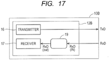
- Fig. 17 is a diagram to explain a controller 10B according to a modification example of the third embodiment.
- the controller 10B includes a signal processing unit 12B.
- the signal processing unit 12B includes a transmitter 16, adjuster 19, and a receiver 17.
- the transmitter 16 transmits data to the bus BS1 through a DALI communication interface module 4.
- the receiver 17 receives data from the bus BS1 through a DALI communication interface module 4.
- the adjuster 19 adjusts a data waveform received through the DALI communication interface module 4.
- Figs. 18A and 18B are diagrams to explain adjusting the waveform of a data signal received by the receiver 17 according to the modification example of the third embodiment. Referring to Fig.
- FIG. 18A an instance of executing a waveform adjustment upon receiving a data signal representing data "0" is illustrated here.
- the adjuster 19 executes a waveform adjustment to lengthen an "H" level period of a data signal which has been input.
- Fig. 18B an instance of executing a waveform adjustment upon receiving a data signal representing data "1” is illustrated here.
- the adjuster 19 executes a waveform adjustment to lengthen an "L" level period of a data signal which has been input.
- Figs. 19A and 19B are other diagrams to explain adjusting the waveform of a data signal received by the receiver 17 according to the modification example of the third embodiment. Referring to Fig.
- FIG. 19A an instance of executing a waveform adjustment upon receiving a data signal representing data "0" or “1” is illustrated here.
- the adjuster 19 executes a waveform adjustment to lengthen an "H" level period of a data signal which has been input.
- FIG. 19B an instance of executing a waveform adjustment upon receiving a data signal representing data "0" or “1” is illustrated here.
- the adjuster 19 executes a waveform adjustment to lengthen an "L” level period of a data signal which has been input.
- a description is provided about an instance of adjusting the receiving side of the first DALI communication interface module 4 in the score table of Fig. 10 .
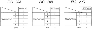
- FIGS. 20A, 20B, and 20C are diagrams to explain a concrete example of a waveform adjustment according to the modification example of the third embodiment.
- Fig. 20A presented are score values at the receiving side of the first DALI communication interface module 4 in the score table of Fig. 10 .
- a maximum score value of 6 is presented here as an example.
- an instance where the score values are decreased by a waveform adjustment of a data signal by the adjuster 19, as described previously, is illustrated, as in Figs. 20B and 20C .
- an adjustment can be made according to the same method as described with Fig. 16 .
- the server 2 checks the score table as described with Fig. 10 .
- the server 2 specifies a DALI communication interface module 4 for which a score value is more than a predetermined threshold, as described with Fig. 10 , by way of example.
- a predetermined threshold as described with Fig. 10
- the server 2 gives an adjustment command.
- the server 2 outputs a command to make a waveform adjustment to the first controller 10-1 via the bus BS2.
- the adjuster 19 within the controller 10-1 executes an adjustment to shorten an "L level or "H" level period of a received data signal.
- the server 2 gives a command to transmit a signal.
- the server 2 outputs a command to output a transmission signal for test use to the respective controllers 10 via the bus BS2.
- the first controller 10-1 receives transmission signals for test use which have accordingly been transmitted from the respective controllers 10 and performs a deterioration judgment for data.
- the server 2 acquires score values transmitted from the controller 10-1 and judges whether or not the score values are more than a threshold.
- the server 2 judges whether or not the score values of received signals of data transmitted from the respective controllers 10 are more than a threshold of "5". If the server 2 has judged that the acquired score values (if any) are more than the threshold, the server 2 outputs a command to make a waveform readjustment to the first controller 10-1 via the bus BS2.
- the adjuster 19 within the controller 10-1 executes an adjustment to shorten an "L" level or "H” level period of a received data signal.
- communication quality can be improved by adjusting the waveform of a signal transferred between DALI communication interface modules.
- FIGs. 21A and 21B are diagrams to explain another method of judging whether a 1-bit data waveform deteriorates according to a fourth embodiment.
- a window width a predetermined interval for data detection is set.
- Interval TO is set as an initial value.
- the window width is adjustable by TO + m ⁇ ⁇ T (m: a positive integer) .
- the window width becomes wider to the right and to the left around the reference position, as m increases. That is, the interval for data detection becomes longer. Therefore, a judgment can be made such that, if m is smaller (the window width is narrower), the data waveform deteriorates to a small extent; if m is larger (the window width is wider), the data waveform deteriorates to a large extent.
- Fig. 21B an instance of judging whether a data waveform for data "0" deteriorates is illustrated. As a window width and as a predetermined interval for data detection, T0 + 2 ⁇ ⁇ T is set.
- the window width becomes wider to the right, as m increases. That is, the interval for data detection becomes longer. Therefore, a judgment can be made such that, if m is smaller (the window width is narrower), the data waveform deteriorates to a small extent; if m is larger (the window width is wider), the data waveform deteriorates to a large extent.
- Fig. 22 is a diagram to explain a method of judging whether a data waveform deteriorates according to a fifth embodiment. Referring to Fig. 22 , a timing window width is set even in an edge portion coinciding with a bit boundary. By setting a timing window in an edge portion coinciding with a bit boundary, it is enabled to detect deterioration of a data waveform with a high degree of accuracy.
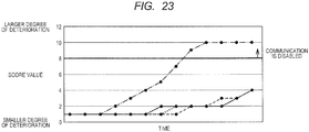
- Fig. 23 is a diagram to explain a score board over a course of time according to a sixth embodiment. Referring to Fig. 23 , an instance where a score value changes over time is illustrated. A score value over which communication is disabled is also presented. In the present example, an instance is illustrated in which a threshold of "8" is set, as an example.
- a DALI communication interface module 4 for which a score value indicates deterioration at a higher speed as illustrated in Fig. 23 , it would become possible to suppress deterioration of communication quality
- a DALI communication interface module 4 for which a score value indicates a deterioration speed higher than a given speed may be specified.
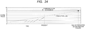
- FIG. 24 is a diagram to explain another example of a score board over a course of time according to the sixth embodiment.
- a prediction line along which a score value will change over time is calculated.
- a day on which the score value will become equal to a threshold of "8" (a day of predicted deterioration failure) is estimated.
- the server 2 may alert and inform an administrator (user) of that day.
- the threshold of "8" can be adjusted optionally. By setting the threshold to a value indicating a phase before the occurrence of a communication disabled state, replacement or repair may be allowed to be performed safely, while communication quality is assured.
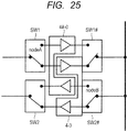
- Fig. 25 is a diagram to explain a part of a light source control system according to a seventh embodiment.
- DALI communication interface modules 4, 4# are provided and switches S1, SW1#, SW2, SW2# are provided.
- Switches SW1, SW1# perform switching for a transmitting-side mechanism of the DALI communication interface modules 4, 4#.
- Switches SW2, SW2# perform switching for a receiving-side mechanism of the DALI communication interface modules 4, 4#.
Landscapes
- Engineering & Computer Science (AREA)
- Quality & Reliability (AREA)
- Computer Networks & Wireless Communication (AREA)
- Signal Processing (AREA)
- Physics & Mathematics (AREA)
- General Physics & Mathematics (AREA)
- Circuit Arrangement For Electric Light Sources In General (AREA)
- Optical Communication System (AREA)
- Dc Digital Transmission (AREA)
- Maintenance And Management Of Digital Transmission (AREA)
- Small-Scale Networks (AREA)
Claims (5)
- Système de commande de source de lumière comprenant un serveur (2) et un dispositif à semi-conducteur qui doit être couplé à une source de lumière (3), le dispositif à semi-conducteur comprenant :une unité de traitement de signal (12) qui doit être couplée à un module d'interface (4, 5) et transmet et reçoit un signal d'ordre pour augmenter ou diminuer une intensité d'illumination de la source de lumière (3) ;le système de commande de source de lumière étant caractérisé en ce que le dispositif à semi-conducteur comprend en outreun détecteur de détérioration (13) qui détecte un degré de détérioration du module d'interface (4, 5) ;dans lequel le détecteur de détérioration (13) détermine le degré de détérioration à partir du fait que le minutage auquel le niveau de tension du signal d'ordre reçu par le module d'interface (4, 5) change du niveau « H » au niveau « L » ou du niveau « L » au niveau « H » est ou non au sein d'une fenêtre de minutage prédéterminée ; et le serveur (2) comprendune table de score qui stocke le degré de détérioration ;dans lequel la table de score stocke en outre les changements de degré de détérioration au cours du temps.
- Système de commande de source de lumière selon la revendication 1, comprenant en outre une unité de pilotage (11) qui commande l'intensité d'illumination de la source de lumière (3), sur la base du signal d'ordre reçu par l'unité de traitement de signal (12).
- Système de commande de source de lumière selon la revendication 1, dans lequel une longueur de la fenêtre de minutage prédéterminée est réglable selon un niveau de réglage.
- Système de commande de source de lumière selon la revendication 1, comprenant en outre un dispositif de réglage (15) qui règle le minutage auquel le signal d'ordre est transmis et reçu par l'unité de traitement de signal (12) sur la base d'un résultat de détection par le détecteur de détérioration (13).
- Système de commande de source de lumière selon la revendication 1, dans lequel le détecteur de détérioration (13) détermine en outre le degré de détérioration du module d'interface (4, 5), sur la base du fait qu'un deuxième minutage auquel le niveau de tension du signal d'ordre reçu par le module d'interface (4, 5) et représentant une limite binaire change du niveau « H » au niveau « L » ou du niveau « L » au niveau « H » est ou non au sein d'une deuxième fenêtre de minutage prédéterminée.
Applications Claiming Priority (1)
| Application Number | Priority Date | Filing Date | Title |
|---|---|---|---|
| JP2016042488A JP6660773B2 (ja) | 2016-03-04 | 2016-03-04 | 半導体装置、光源制御装置および光源制御システム |
Publications (2)
| Publication Number | Publication Date |
|---|---|
| EP3214905A1 EP3214905A1 (fr) | 2017-09-06 |
| EP3214905B1 true EP3214905B1 (fr) | 2020-10-07 |
Family
ID=58159004
Family Applications (1)
| Application Number | Title | Priority Date | Filing Date |
|---|---|---|---|
| EP17157899.0A Active EP3214905B1 (fr) | 2016-03-04 | 2017-02-24 | Dispositif semi-conducteur, dispositif de commande de source de lumière et système de commande de source de lumière |
Country Status (4)
| Country | Link |
|---|---|
| US (1) | US10231315B2 (fr) |
| EP (1) | EP3214905B1 (fr) |
| JP (1) | JP6660773B2 (fr) |
| CN (1) | CN107155247B (fr) |
Family Cites Families (19)
| Publication number | Priority date | Publication date | Assignee | Title |
|---|---|---|---|---|
| JPS5769228A (en) * | 1980-10-18 | 1982-04-27 | Fuji Electric Co Ltd | Deterioration detection system for optical transmitting circuit |
| JPH10255185A (ja) * | 1997-03-12 | 1998-09-25 | Hochiki Corp | 火災検知器の動作試験方法及び火災検知器動作試験装置 |
| JP2002324684A (ja) * | 2001-04-25 | 2002-11-08 | Matsushita Electric Works Ltd | 照明制御装置 |
| JP5135767B2 (ja) * | 2006-11-09 | 2013-02-06 | ソニー株式会社 | データ受信装置 |
| JP2008268002A (ja) * | 2007-04-20 | 2008-11-06 | Fuji Electric Device Technology Co Ltd | フォトカプラの寿命予測装置、電力変換装置およびフォトカプラの寿命予測方法 |
| JP5197241B2 (ja) * | 2008-09-01 | 2013-05-15 | ルネサスエレクトロニクス株式会社 | 半導体装置 |
| US8680969B2 (en) * | 2009-03-20 | 2014-03-25 | Lutron Electronics Co., Inc. | Method of confirming that a control device complies with a predefined protocol standard |
| JP2011076025A (ja) * | 2009-10-02 | 2011-04-14 | Sony Corp | 表示装置、表示装置の駆動方法および電子機器 |
| CN101790272B (zh) * | 2010-03-02 | 2013-03-20 | 四川锦明光电股份有限公司 | 具有冗余容错功能的led光源驱动器 |
| KR101188099B1 (ko) * | 2010-09-08 | 2012-10-05 | 한국과학기술원 | 리세트 기능을 갖는 액티브 유기 발광 디스플레이 |
| JP2012175751A (ja) * | 2011-02-18 | 2012-09-10 | Panasonic Corp | 配電システム |
| JP5842127B2 (ja) | 2011-06-22 | 2016-01-13 | パナソニックIpマネジメント株式会社 | 照明装置、照明制御装置、照明器具及び照明制御システム |
| WO2013001432A1 (fr) * | 2011-06-29 | 2013-01-03 | Koninklijke Philips Electronics N.V. | Réseau d'éclairage intelligent pour générer des avatars lumineux |
| WO2014013454A2 (fr) * | 2012-07-20 | 2014-01-23 | Koninklijke Philips N.V. | Circuit d'interface de communication numérique pour paire de lignes à compensation de déséquilibre de rapport cyclique |
| JP2014067486A (ja) * | 2012-09-24 | 2014-04-17 | Toshiba Lighting & Technology Corp | 照明装置、照明器具および照明システム |
| JP2014072832A (ja) * | 2012-10-01 | 2014-04-21 | Azbil Corp | デジタル伝送モジュール |
| US9439270B2 (en) * | 2012-10-17 | 2016-09-06 | Koninklijke Philips N.V. | Digital communication receiver interface circuit for line-pair with duty cycle imbalance compensation |
| JP6127566B2 (ja) * | 2013-02-18 | 2017-05-17 | 三菱電機株式会社 | 光源点灯装置およびこれを用いた照明装置 |
| US20170181240A1 (en) * | 2015-12-16 | 2017-06-22 | General Electric Company | High voltage resistant transmitting circuit for devices communicating on dali bus |
-
2016
- 2016-03-04 JP JP2016042488A patent/JP6660773B2/ja active Active
- 2016-12-25 US US15/390,530 patent/US10231315B2/en active Active
-
2017
- 2017-02-10 CN CN201710072303.8A patent/CN107155247B/zh active Active
- 2017-02-24 EP EP17157899.0A patent/EP3214905B1/fr active Active
Non-Patent Citations (1)
| Title |
|---|
| None * |
Also Published As
| Publication number | Publication date |
|---|---|
| US10231315B2 (en) | 2019-03-12 |
| CN107155247B (zh) | 2021-04-20 |
| JP2017158152A (ja) | 2017-09-07 |
| EP3214905A1 (fr) | 2017-09-06 |
| JP6660773B2 (ja) | 2020-03-11 |
| CN107155247A (zh) | 2017-09-12 |
| US20170257931A1 (en) | 2017-09-07 |
Similar Documents
| Publication | Publication Date | Title |
|---|---|---|
| US11632832B2 (en) | Data acquisition methods and apparatus for a network connected LED driver | |
| US11122663B2 (en) | Monitoring lighting | |
| US9474138B2 (en) | Failure detection in lighting system | |
| US11328580B2 (en) | Testing of a network of hazard warning devices | |
| US9524641B2 (en) | LED traffic signal fault logging system and method | |
| RU2614037C1 (ru) | Устройство управления источниками света и способ управления источниками света | |
| US20170090549A1 (en) | Switch control device and method for power | |
| EP3214905B1 (fr) | Dispositif semi-conducteur, dispositif de commande de source de lumière et système de commande de source de lumière | |
| CN117856440A (zh) | 电压传输损耗补偿系统及方法 | |
| CN111837362B (zh) | 用于串行总线系统的用户站和用于在串行总线系统中进行数据传输的方法 | |
| US9629222B2 (en) | Digital addressable lighting interface short protection circuit | |
| US11632842B2 (en) | Selective inrush current control with active current clamp and monitoring | |
| US10869226B2 (en) | Wireless communication apparatus, wireless communication system and wireless communication method | |
| JP6586382B2 (ja) | 光源制御システム | |
| US20200367343A1 (en) | Multi-Channel Dimmer | |
| CN115561565A (zh) | 一种基于网络通信的高压变频器监测装置及方法 | |
| US20170256341A1 (en) | Control circuit and control method | |
| US10574514B2 (en) | Duplex control device and duplex system | |
| KR102856029B1 (ko) | 시선 유도등 및 시선 유도등 제어 시스템 | |
| US20180331680A1 (en) | Switch control device and method for power | |
| US12451923B2 (en) | Transceiver for coupling to a galvanically isolated bus | |
| JP7312714B2 (ja) | 信号情報送信装置 | |
| JP5182928B2 (ja) | 電気接続箱およびデータ取得方法 | |
| US20050248298A1 (en) | Duplexing protection apparatus and operation method thereof | |
| US20170063581A1 (en) | Method of demodulating a signal packet, a communication system and a lighting device |
Legal Events
| Date | Code | Title | Description |
|---|---|---|---|
| PUAI | Public reference made under article 153(3) epc to a published international application that has entered the european phase |
Free format text: ORIGINAL CODE: 0009012 |
|
| STAA | Information on the status of an ep patent application or granted ep patent |
Free format text: STATUS: THE APPLICATION HAS BEEN PUBLISHED |
|
| AK | Designated contracting states |
Kind code of ref document: A1 Designated state(s): AL AT BE BG CH CY CZ DE DK EE ES FI FR GB GR HR HU IE IS IT LI LT LU LV MC MK MT NL NO PL PT RO RS SE SI SK SM TR |
|
| AX | Request for extension of the european patent |
Extension state: BA ME |
|
| STAA | Information on the status of an ep patent application or granted ep patent |
Free format text: STATUS: REQUEST FOR EXAMINATION WAS MADE |
|
| 17P | Request for examination filed |
Effective date: 20180306 |
|
| RBV | Designated contracting states (corrected) |
Designated state(s): AL AT BE BG CH CY CZ DE DK EE ES FI FR GB GR HR HU IE IS IT LI LT LU LV MC MK MT NL NO PL PT RO RS SE SI SK SM TR |
|
| STAA | Information on the status of an ep patent application or granted ep patent |
Free format text: STATUS: EXAMINATION IS IN PROGRESS |
|
| 17Q | First examination report despatched |
Effective date: 20190527 |
|
| REG | Reference to a national code |
Ref country code: DE Ref legal event code: R079 Ref document number: 602017024846 Country of ref document: DE Free format text: PREVIOUS MAIN CLASS: H05B0037020000 Ipc: H05B0047180000 |
|
| RIC1 | Information provided on ipc code assigned before grant |
Ipc: H05B 47/18 20200101AFI20200415BHEP Ipc: G01R 29/027 20060101ALI20200415BHEP Ipc: H04L 1/20 20060101ALI20200415BHEP |
|
| GRAP | Despatch of communication of intention to grant a patent |
Free format text: ORIGINAL CODE: EPIDOSNIGR1 |
|
| STAA | Information on the status of an ep patent application or granted ep patent |
Free format text: STATUS: GRANT OF PATENT IS INTENDED |
|
| INTG | Intention to grant announced |
Effective date: 20200626 |
|
| GRAS | Grant fee paid |
Free format text: ORIGINAL CODE: EPIDOSNIGR3 |
|
| GRAA | (expected) grant |
Free format text: ORIGINAL CODE: 0009210 |
|
| STAA | Information on the status of an ep patent application or granted ep patent |
Free format text: STATUS: THE PATENT HAS BEEN GRANTED |
|
| AK | Designated contracting states |
Kind code of ref document: B1 Designated state(s): AL AT BE BG CH CY CZ DE DK EE ES FI FR GB GR HR HU IE IS IT LI LT LU LV MC MK MT NL NO PL PT RO RS SE SI SK SM TR |
|
| REG | Reference to a national code |
Ref country code: GB Ref legal event code: FG4D |
|
| REG | Reference to a national code |
Ref country code: AT Ref legal event code: REF Ref document number: 1322614 Country of ref document: AT Kind code of ref document: T Effective date: 20201015 Ref country code: CH Ref legal event code: EP |
|
| REG | Reference to a national code |
Ref country code: IE Ref legal event code: FG4D |
|
| REG | Reference to a national code |
Ref country code: DE Ref legal event code: R096 Ref document number: 602017024846 Country of ref document: DE |
|
| REG | Reference to a national code |
Ref country code: NL Ref legal event code: MP Effective date: 20201007 |
|
| REG | Reference to a national code |
Ref country code: AT Ref legal event code: MK05 Ref document number: 1322614 Country of ref document: AT Kind code of ref document: T Effective date: 20201007 |
|
| PG25 | Lapsed in a contracting state [announced via postgrant information from national office to epo] |
Ref country code: GR Free format text: LAPSE BECAUSE OF FAILURE TO SUBMIT A TRANSLATION OF THE DESCRIPTION OR TO PAY THE FEE WITHIN THE PRESCRIBED TIME-LIMIT Effective date: 20210108 Ref country code: FI Free format text: LAPSE BECAUSE OF FAILURE TO SUBMIT A TRANSLATION OF THE DESCRIPTION OR TO PAY THE FEE WITHIN THE PRESCRIBED TIME-LIMIT Effective date: 20201007 Ref country code: PT Free format text: LAPSE BECAUSE OF FAILURE TO SUBMIT A TRANSLATION OF THE DESCRIPTION OR TO PAY THE FEE WITHIN THE PRESCRIBED TIME-LIMIT Effective date: 20210208 Ref country code: RS Free format text: LAPSE BECAUSE OF FAILURE TO SUBMIT A TRANSLATION OF THE DESCRIPTION OR TO PAY THE FEE WITHIN THE PRESCRIBED TIME-LIMIT Effective date: 20201007 Ref country code: NL Free format text: LAPSE BECAUSE OF FAILURE TO SUBMIT A TRANSLATION OF THE DESCRIPTION OR TO PAY THE FEE WITHIN THE PRESCRIBED TIME-LIMIT Effective date: 20201007 Ref country code: NO Free format text: LAPSE BECAUSE OF FAILURE TO SUBMIT A TRANSLATION OF THE DESCRIPTION OR TO PAY THE FEE WITHIN THE PRESCRIBED TIME-LIMIT Effective date: 20210107 |
|
| REG | Reference to a national code |
Ref country code: LT Ref legal event code: MG4D |
|
| PG25 | Lapsed in a contracting state [announced via postgrant information from national office to epo] |
Ref country code: SE Free format text: LAPSE BECAUSE OF FAILURE TO SUBMIT A TRANSLATION OF THE DESCRIPTION OR TO PAY THE FEE WITHIN THE PRESCRIBED TIME-LIMIT Effective date: 20201007 Ref country code: BG Free format text: LAPSE BECAUSE OF FAILURE TO SUBMIT A TRANSLATION OF THE DESCRIPTION OR TO PAY THE FEE WITHIN THE PRESCRIBED TIME-LIMIT Effective date: 20210107 Ref country code: PL Free format text: LAPSE BECAUSE OF FAILURE TO SUBMIT A TRANSLATION OF THE DESCRIPTION OR TO PAY THE FEE WITHIN THE PRESCRIBED TIME-LIMIT Effective date: 20201007 Ref country code: LV Free format text: LAPSE BECAUSE OF FAILURE TO SUBMIT A TRANSLATION OF THE DESCRIPTION OR TO PAY THE FEE WITHIN THE PRESCRIBED TIME-LIMIT Effective date: 20201007 Ref country code: IS Free format text: LAPSE BECAUSE OF FAILURE TO SUBMIT A TRANSLATION OF THE DESCRIPTION OR TO PAY THE FEE WITHIN THE PRESCRIBED TIME-LIMIT Effective date: 20210207 Ref country code: AT Free format text: LAPSE BECAUSE OF FAILURE TO SUBMIT A TRANSLATION OF THE DESCRIPTION OR TO PAY THE FEE WITHIN THE PRESCRIBED TIME-LIMIT Effective date: 20201007 Ref country code: ES Free format text: LAPSE BECAUSE OF FAILURE TO SUBMIT A TRANSLATION OF THE DESCRIPTION OR TO PAY THE FEE WITHIN THE PRESCRIBED TIME-LIMIT Effective date: 20201007 |
|
| PG25 | Lapsed in a contracting state [announced via postgrant information from national office to epo] |
Ref country code: HR Free format text: LAPSE BECAUSE OF FAILURE TO SUBMIT A TRANSLATION OF THE DESCRIPTION OR TO PAY THE FEE WITHIN THE PRESCRIBED TIME-LIMIT Effective date: 20201007 |
|
| REG | Reference to a national code |
Ref country code: DE Ref legal event code: R097 Ref document number: 602017024846 Country of ref document: DE |
|
| PG25 | Lapsed in a contracting state [announced via postgrant information from national office to epo] |
Ref country code: RO Free format text: LAPSE BECAUSE OF FAILURE TO SUBMIT A TRANSLATION OF THE DESCRIPTION OR TO PAY THE FEE WITHIN THE PRESCRIBED TIME-LIMIT Effective date: 20201007 Ref country code: SK Free format text: LAPSE BECAUSE OF FAILURE TO SUBMIT A TRANSLATION OF THE DESCRIPTION OR TO PAY THE FEE WITHIN THE PRESCRIBED TIME-LIMIT Effective date: 20201007 Ref country code: EE Free format text: LAPSE BECAUSE OF FAILURE TO SUBMIT A TRANSLATION OF THE DESCRIPTION OR TO PAY THE FEE WITHIN THE PRESCRIBED TIME-LIMIT Effective date: 20201007 Ref country code: CZ Free format text: LAPSE BECAUSE OF FAILURE TO SUBMIT A TRANSLATION OF THE DESCRIPTION OR TO PAY THE FEE WITHIN THE PRESCRIBED TIME-LIMIT Effective date: 20201007 Ref country code: SM Free format text: LAPSE BECAUSE OF FAILURE TO SUBMIT A TRANSLATION OF THE DESCRIPTION OR TO PAY THE FEE WITHIN THE PRESCRIBED TIME-LIMIT Effective date: 20201007 Ref country code: LT Free format text: LAPSE BECAUSE OF FAILURE TO SUBMIT A TRANSLATION OF THE DESCRIPTION OR TO PAY THE FEE WITHIN THE PRESCRIBED TIME-LIMIT Effective date: 20201007 |
|
| PLBE | No opposition filed within time limit |
Free format text: ORIGINAL CODE: 0009261 |
|
| STAA | Information on the status of an ep patent application or granted ep patent |
Free format text: STATUS: NO OPPOSITION FILED WITHIN TIME LIMIT |
|
| PG25 | Lapsed in a contracting state [announced via postgrant information from national office to epo] |
Ref country code: DK Free format text: LAPSE BECAUSE OF FAILURE TO SUBMIT A TRANSLATION OF THE DESCRIPTION OR TO PAY THE FEE WITHIN THE PRESCRIBED TIME-LIMIT Effective date: 20201007 |
|
| 26N | No opposition filed |
Effective date: 20210708 |
|
| PG25 | Lapsed in a contracting state [announced via postgrant information from national office to epo] |
Ref country code: MC Free format text: LAPSE BECAUSE OF FAILURE TO SUBMIT A TRANSLATION OF THE DESCRIPTION OR TO PAY THE FEE WITHIN THE PRESCRIBED TIME-LIMIT Effective date: 20201007 |
|
| GBPC | Gb: european patent ceased through non-payment of renewal fee |
Effective date: 20210224 |
|
| REG | Reference to a national code |
Ref country code: BE Ref legal event code: MM Effective date: 20210228 |
|
| PG25 | Lapsed in a contracting state [announced via postgrant information from national office to epo] |
Ref country code: AL Free format text: LAPSE BECAUSE OF FAILURE TO SUBMIT A TRANSLATION OF THE DESCRIPTION OR TO PAY THE FEE WITHIN THE PRESCRIBED TIME-LIMIT Effective date: 20201007 Ref country code: CH Free format text: LAPSE BECAUSE OF NON-PAYMENT OF DUE FEES Effective date: 20210228 Ref country code: IT Free format text: LAPSE BECAUSE OF FAILURE TO SUBMIT A TRANSLATION OF THE DESCRIPTION OR TO PAY THE FEE WITHIN THE PRESCRIBED TIME-LIMIT Effective date: 20201007 Ref country code: LU Free format text: LAPSE BECAUSE OF NON-PAYMENT OF DUE FEES Effective date: 20210224 Ref country code: LI Free format text: LAPSE BECAUSE OF NON-PAYMENT OF DUE FEES Effective date: 20210228 |
|
| PG25 | Lapsed in a contracting state [announced via postgrant information from national office to epo] |
Ref country code: SI Free format text: LAPSE BECAUSE OF FAILURE TO SUBMIT A TRANSLATION OF THE DESCRIPTION OR TO PAY THE FEE WITHIN THE PRESCRIBED TIME-LIMIT Effective date: 20201007 |
|
| PG25 | Lapsed in a contracting state [announced via postgrant information from national office to epo] |
Ref country code: FR Free format text: LAPSE BECAUSE OF NON-PAYMENT OF DUE FEES Effective date: 20210228 Ref country code: IE Free format text: LAPSE BECAUSE OF NON-PAYMENT OF DUE FEES Effective date: 20210224 Ref country code: GB Free format text: LAPSE BECAUSE OF NON-PAYMENT OF DUE FEES Effective date: 20210224 |
|
| PG25 | Lapsed in a contracting state [announced via postgrant information from national office to epo] |
Ref country code: IS Free format text: LAPSE BECAUSE OF FAILURE TO SUBMIT A TRANSLATION OF THE DESCRIPTION OR TO PAY THE FEE WITHIN THE PRESCRIBED TIME-LIMIT Effective date: 20210207 |
|
| PG25 | Lapsed in a contracting state [announced via postgrant information from national office to epo] |
Ref country code: BE Free format text: LAPSE BECAUSE OF NON-PAYMENT OF DUE FEES Effective date: 20210228 |
|
| PG25 | Lapsed in a contracting state [announced via postgrant information from national office to epo] |
Ref country code: HU Free format text: LAPSE BECAUSE OF FAILURE TO SUBMIT A TRANSLATION OF THE DESCRIPTION OR TO PAY THE FEE WITHIN THE PRESCRIBED TIME-LIMIT; INVALID AB INITIO Effective date: 20170224 |
|
| PG25 | Lapsed in a contracting state [announced via postgrant information from national office to epo] |
Ref country code: CY Free format text: LAPSE BECAUSE OF FAILURE TO SUBMIT A TRANSLATION OF THE DESCRIPTION OR TO PAY THE FEE WITHIN THE PRESCRIBED TIME-LIMIT Effective date: 20201007 |
|
| PG25 | Lapsed in a contracting state [announced via postgrant information from national office to epo] |
Ref country code: MK Free format text: LAPSE BECAUSE OF FAILURE TO SUBMIT A TRANSLATION OF THE DESCRIPTION OR TO PAY THE FEE WITHIN THE PRESCRIBED TIME-LIMIT Effective date: 20201007 |
|
| PG25 | Lapsed in a contracting state [announced via postgrant information from national office to epo] |
Ref country code: TR Free format text: LAPSE BECAUSE OF FAILURE TO SUBMIT A TRANSLATION OF THE DESCRIPTION OR TO PAY THE FEE WITHIN THE PRESCRIBED TIME-LIMIT Effective date: 20201007 |
|
| PG25 | Lapsed in a contracting state [announced via postgrant information from national office to epo] |
Ref country code: MT Free format text: LAPSE BECAUSE OF FAILURE TO SUBMIT A TRANSLATION OF THE DESCRIPTION OR TO PAY THE FEE WITHIN THE PRESCRIBED TIME-LIMIT Effective date: 20201007 |
|
| PGFP | Annual fee paid to national office [announced via postgrant information from national office to epo] |
Ref country code: DE Payment date: 20260220 Year of fee payment: 10 |