EP3214906A1 - Generator für elektrische entladungen und energieversorgungsvorrichtung dafür - Google Patents
Generator für elektrische entladungen und energieversorgungsvorrichtung dafür Download PDFInfo
- Publication number
- EP3214906A1 EP3214906A1 EP14904944.7A EP14904944A EP3214906A1 EP 3214906 A1 EP3214906 A1 EP 3214906A1 EP 14904944 A EP14904944 A EP 14904944A EP 3214906 A1 EP3214906 A1 EP 3214906A1
- Authority
- EP
- European Patent Office
- Prior art keywords
- radical gas
- gas
- radical
- power supply
- target object
- Prior art date
- Legal status (The legal status is an assumption and is not a legal conclusion. Google has not performed a legal analysis and makes no representation as to the accuracy of the status listed.)
- Granted
Links
Images


Classifications
-
- C—CHEMISTRY; METALLURGY
- C23—COATING METALLIC MATERIAL; COATING MATERIAL WITH METALLIC MATERIAL; CHEMICAL SURFACE TREATMENT; DIFFUSION TREATMENT OF METALLIC MATERIAL; COATING BY VACUUM EVAPORATION, BY SPUTTERING, BY ION IMPLANTATION OR BY CHEMICAL VAPOUR DEPOSITION, IN GENERAL; INHIBITING CORROSION OF METALLIC MATERIAL OR INCRUSTATION IN GENERAL
- C23C—COATING METALLIC MATERIAL; COATING MATERIAL WITH METALLIC MATERIAL; SURFACE TREATMENT OF METALLIC MATERIAL BY DIFFUSION INTO THE SURFACE, BY CHEMICAL CONVERSION OR SUBSTITUTION; COATING BY VACUUM EVAPORATION, BY SPUTTERING, BY ION IMPLANTATION OR BY CHEMICAL VAPOUR DEPOSITION, IN GENERAL
- C23C16/00—Chemical coating by decomposition of gaseous compounds, without leaving reaction products of surface material in the coating, i.e. chemical vapour deposition [CVD] processes
- C23C16/44—Chemical coating by decomposition of gaseous compounds, without leaving reaction products of surface material in the coating, i.e. chemical vapour deposition [CVD] processes characterised by the method of coating
- C23C16/50—Chemical coating by decomposition of gaseous compounds, without leaving reaction products of surface material in the coating, i.e. chemical vapour deposition [CVD] processes characterised by the method of coating using electric discharges
- C23C16/503—Chemical coating by decomposition of gaseous compounds, without leaving reaction products of surface material in the coating, i.e. chemical vapour deposition [CVD] processes characterised by the method of coating using electric discharges using DC or AC discharges
-
- C—CHEMISTRY; METALLURGY
- C23—COATING METALLIC MATERIAL; COATING MATERIAL WITH METALLIC MATERIAL; CHEMICAL SURFACE TREATMENT; DIFFUSION TREATMENT OF METALLIC MATERIAL; COATING BY VACUUM EVAPORATION, BY SPUTTERING, BY ION IMPLANTATION OR BY CHEMICAL VAPOUR DEPOSITION, IN GENERAL; INHIBITING CORROSION OF METALLIC MATERIAL OR INCRUSTATION IN GENERAL
- C23C—COATING METALLIC MATERIAL; COATING MATERIAL WITH METALLIC MATERIAL; SURFACE TREATMENT OF METALLIC MATERIAL BY DIFFUSION INTO THE SURFACE, BY CHEMICAL CONVERSION OR SUBSTITUTION; COATING BY VACUUM EVAPORATION, BY SPUTTERING, BY ION IMPLANTATION OR BY CHEMICAL VAPOUR DEPOSITION, IN GENERAL
- C23C16/00—Chemical coating by decomposition of gaseous compounds, without leaving reaction products of surface material in the coating, i.e. chemical vapour deposition [CVD] processes
- C23C16/22—Chemical coating by decomposition of gaseous compounds, without leaving reaction products of surface material in the coating, i.e. chemical vapour deposition [CVD] processes characterised by the deposition of inorganic material, other than metallic material
- C23C16/30—Deposition of compounds, mixtures or solid solutions, e.g. borides, carbides, nitrides
- C23C16/34—Nitrides
-
- C—CHEMISTRY; METALLURGY
- C23—COATING METALLIC MATERIAL; COATING MATERIAL WITH METALLIC MATERIAL; CHEMICAL SURFACE TREATMENT; DIFFUSION TREATMENT OF METALLIC MATERIAL; COATING BY VACUUM EVAPORATION, BY SPUTTERING, BY ION IMPLANTATION OR BY CHEMICAL VAPOUR DEPOSITION, IN GENERAL; INHIBITING CORROSION OF METALLIC MATERIAL OR INCRUSTATION IN GENERAL
- C23C—COATING METALLIC MATERIAL; COATING MATERIAL WITH METALLIC MATERIAL; SURFACE TREATMENT OF METALLIC MATERIAL BY DIFFUSION INTO THE SURFACE, BY CHEMICAL CONVERSION OR SUBSTITUTION; COATING BY VACUUM EVAPORATION, BY SPUTTERING, BY ION IMPLANTATION OR BY CHEMICAL VAPOUR DEPOSITION, IN GENERAL
- C23C16/00—Chemical coating by decomposition of gaseous compounds, without leaving reaction products of surface material in the coating, i.e. chemical vapour deposition [CVD] processes
- C23C16/44—Chemical coating by decomposition of gaseous compounds, without leaving reaction products of surface material in the coating, i.e. chemical vapour deposition [CVD] processes characterised by the method of coating
- C23C16/458—Chemical coating by decomposition of gaseous compounds, without leaving reaction products of surface material in the coating, i.e. chemical vapour deposition [CVD] processes characterised by the method of coating characterised by the method used for supporting substrates in the reaction chamber
- C23C16/4582—Rigid and flat substrates, e.g. plates or discs
- C23C16/4587—Rigid and flat substrates, e.g. plates or discs the substrate being supported substantially vertically
- C23C16/4588—Rigid and flat substrates, e.g. plates or discs the substrate being supported substantially vertically the substrate being rotated
-
- C—CHEMISTRY; METALLURGY
- C23—COATING METALLIC MATERIAL; COATING MATERIAL WITH METALLIC MATERIAL; CHEMICAL SURFACE TREATMENT; DIFFUSION TREATMENT OF METALLIC MATERIAL; COATING BY VACUUM EVAPORATION, BY SPUTTERING, BY ION IMPLANTATION OR BY CHEMICAL VAPOUR DEPOSITION, IN GENERAL; INHIBITING CORROSION OF METALLIC MATERIAL OR INCRUSTATION IN GENERAL
- C23C—COATING METALLIC MATERIAL; COATING MATERIAL WITH METALLIC MATERIAL; SURFACE TREATMENT OF METALLIC MATERIAL BY DIFFUSION INTO THE SURFACE, BY CHEMICAL CONVERSION OR SUBSTITUTION; COATING BY VACUUM EVAPORATION, BY SPUTTERING, BY ION IMPLANTATION OR BY CHEMICAL VAPOUR DEPOSITION, IN GENERAL
- C23C16/00—Chemical coating by decomposition of gaseous compounds, without leaving reaction products of surface material in the coating, i.e. chemical vapour deposition [CVD] processes
- C23C16/44—Chemical coating by decomposition of gaseous compounds, without leaving reaction products of surface material in the coating, i.e. chemical vapour deposition [CVD] processes characterised by the method of coating
- C23C16/50—Chemical coating by decomposition of gaseous compounds, without leaving reaction products of surface material in the coating, i.e. chemical vapour deposition [CVD] processes characterised by the method of coating using electric discharges
-
- C—CHEMISTRY; METALLURGY
- C23—COATING METALLIC MATERIAL; COATING MATERIAL WITH METALLIC MATERIAL; CHEMICAL SURFACE TREATMENT; DIFFUSION TREATMENT OF METALLIC MATERIAL; COATING BY VACUUM EVAPORATION, BY SPUTTERING, BY ION IMPLANTATION OR BY CHEMICAL VAPOUR DEPOSITION, IN GENERAL; INHIBITING CORROSION OF METALLIC MATERIAL OR INCRUSTATION IN GENERAL
- C23C—COATING METALLIC MATERIAL; COATING MATERIAL WITH METALLIC MATERIAL; SURFACE TREATMENT OF METALLIC MATERIAL BY DIFFUSION INTO THE SURFACE, BY CHEMICAL CONVERSION OR SUBSTITUTION; COATING BY VACUUM EVAPORATION, BY SPUTTERING, BY ION IMPLANTATION OR BY CHEMICAL VAPOUR DEPOSITION, IN GENERAL
- C23C16/00—Chemical coating by decomposition of gaseous compounds, without leaving reaction products of surface material in the coating, i.e. chemical vapour deposition [CVD] processes
- C23C16/44—Chemical coating by decomposition of gaseous compounds, without leaving reaction products of surface material in the coating, i.e. chemical vapour deposition [CVD] processes characterised by the method of coating
- C23C16/52—Controlling or regulating the coating process
-
- H—ELECTRICITY
- H01—ELECTRIC ELEMENTS
- H01J—ELECTRIC DISCHARGE TUBES OR DISCHARGE LAMPS
- H01J37/00—Discharge tubes with provision for introducing objects or material to be exposed to the discharge, e.g. for the purpose of examination or processing thereof
- H01J37/32—Gas-filled discharge tubes
- H01J37/32009—Arrangements for generation of plasma specially adapted for examination or treatment of objects, e.g. plasma sources
- H01J37/32018—Glow discharge
- H01J37/32036—AC powered
-
- H—ELECTRICITY
- H01—ELECTRIC ELEMENTS
- H01J—ELECTRIC DISCHARGE TUBES OR DISCHARGE LAMPS
- H01J37/00—Discharge tubes with provision for introducing objects or material to be exposed to the discharge, e.g. for the purpose of examination or processing thereof
- H01J37/32—Gas-filled discharge tubes
- H01J37/32009—Arrangements for generation of plasma specially adapted for examination or treatment of objects, e.g. plasma sources
- H01J37/32018—Glow discharge
- H01J37/32045—Circuits specially adapted for controlling the glow discharge
-
- H—ELECTRICITY
- H01—ELECTRIC ELEMENTS
- H01J—ELECTRIC DISCHARGE TUBES OR DISCHARGE LAMPS
- H01J37/00—Discharge tubes with provision for introducing objects or material to be exposed to the discharge, e.g. for the purpose of examination or processing thereof
- H01J37/32—Gas-filled discharge tubes
- H01J37/32009—Arrangements for generation of plasma specially adapted for examination or treatment of objects, e.g. plasma sources
- H01J37/32348—Dielectric barrier discharge
-
- H—ELECTRICITY
- H01—ELECTRIC ELEMENTS
- H01J—ELECTRIC DISCHARGE TUBES OR DISCHARGE LAMPS
- H01J37/00—Discharge tubes with provision for introducing objects or material to be exposed to the discharge, e.g. for the purpose of examination or processing thereof
- H01J37/32—Gas-filled discharge tubes
- H01J37/32009—Arrangements for generation of plasma specially adapted for examination or treatment of objects, e.g. plasma sources
- H01J37/32357—Generation remote from the workpiece, e.g. down-stream
-
- H—ELECTRICITY
- H05—ELECTRIC TECHNIQUES NOT OTHERWISE PROVIDED FOR
- H05H—PLASMA TECHNIQUE; PRODUCTION OF ACCELERATED ELECTRICALLY-CHARGED PARTICLES OR OF NEUTRONS; PRODUCTION OR ACCELERATION OF NEUTRAL MOLECULAR OR ATOMIC BEAMS
- H05H1/00—Generating plasma; Handling plasma
- H05H1/24—Generating plasma
- H05H1/46—Generating plasma using applied electromagnetic fields, e.g. high frequency or microwave energy
-
- H—ELECTRICITY
- H10—SEMICONDUCTOR DEVICES; ELECTRIC SOLID-STATE DEVICES NOT OTHERWISE PROVIDED FOR
- H10P—GENERIC PROCESSES OR APPARATUS FOR THE MANUFACTURE OR TREATMENT OF DEVICES COVERED BY CLASS H10
- H10P14/00—Formation of materials, e.g. in the shape of layers or pillars
- H10P14/60—Formation of materials, e.g. in the shape of layers or pillars of insulating materials
-
- H—ELECTRICITY
- H01—ELECTRIC ELEMENTS
- H01J—ELECTRIC DISCHARGE TUBES OR DISCHARGE LAMPS
- H01J2237/00—Discharge tubes exposing object to beam, e.g. for analysis treatment, etching, imaging
- H01J2237/32—Processing objects by plasma generation
- H01J2237/33—Processing objects by plasma generation characterised by the type of processing
- H01J2237/332—Coating
- H01J2237/3321—CVD [Chemical Vapor Deposition]
Definitions
- the present invention relates to an electric discharge generator that includes a power supply device, can generate a radical gas, and can perform a process in which the radical gas is used, and also relates to a power supply device of electric discharge generator.
- the present invention is applicable to, for example, formation of a high-performance film on a target object.
- a need exists for multifunctional, high-quality thin films e.g., highly insulative thin films, semiconductor thin films, highly dielectric thin films, light-emitting thin films, highly magnetic thin films, and superhard thin films.
- high-frequency plasma or microwave plasma is directly generated in the process chamber apparatus.
- the target object is accordingly exposed to a radical gas or plasma ions (or electrons) having a high energy.
- Patent document 1 is an example of related art documents in which techniques associated with plasma CVD apparatuses are disclosed.
- the target object is not damaged by plasma (ions or electrons), and a high-quality film such as a nitride film or oxide film is formed accordingly.
- a high-quality film such as a nitride film or oxide film is formed accordingly.
- the recent thermal and photo CVD apparatuses use, as a source gas, an HN 3 gas or a O 3 gas, which is highly concentrated and readily dissociated by radiation of heat or light.
- a thermal catalyst is provided in a CVD chamber apparatus.
- a catalytic action promotes dissociation of the gas in the thermal and photo CVD apparatus, whereby a film such as a nitride film or an oxide film can be formed in a short time.
- this saves only a limited amount of time, and thus, it is difficult to accelerate the film formation significantly.
- An example of apparatuses that can reduce damages to the target object caused by plasma and can further accelerate the film formation is a film formation process apparatus of remote plasma type (see, for example, Patent Document 2).
- a plasma generation region and a target object process region are separated by a partition (plasma confining electrode).
- the plasma confining electrode is located between a high-frequency application electrode and a counter electrode on which a target object is placed.
- the technique disclosed in Patent Document 2 provides the target object with only neutral activated species.
- part of a source gas is activated by plasma in a remote plasma source.
- a gas channel circles around in a loop.
- An active gas generated in the remote plasma source is discharged and supplied to the apparatus in which a target object is placed.
- Various source gases such as a nitrogen gas, an oxygen gas, an ozone gas, or a hydrogen gas may be used in the thin film technique according to Patent Document 3 and the like.
- An activated radical gas is generated from the source gas, and then, a thin film is formed on a target object through the use of the radical gas.
- the radical gas is highly reactive.
- the radical gas in minute quantities (at a concentration less than or equal to about 1%: 1000 ppm) is sprayed onto a target object to promote a chemical reaction in the target object, whereby a film such as a nitrogen thin film, an oxide thin film, or a hydrogen-bonding thin film can be efficiently formed in a short time.
- a radical gas generation apparatus includes discharge cells (generators). In the discharge cells, high-field plasma is created through the use of a dielectric barrier discharge, which is atmospheric pressure plasma. Consequently, a high-quality radical gas is generated from the source gas exposed to the plasma in the discharge cells.
- the plurality of discharge cells are disposed in the radical gas generation apparatus, so that the generated radical gas is sprayed in many different quarters and the resultant radical gas becomes available for use.
- the conventional radical gas generation apparatuses fail to generate an effective, highly reactive radical gas. Further, it is difficult to obtain a radical gas in large quantities and the radical gas is supplied from one direction. In addition, the lifetime of the generated radical gas is very short. Thus, it is difficult to minimize a decrease in concentration and to conduct a radical from the radical gas generation apparatus to a radical gas process area (a thin film generation area, namely, a process chamber apparatus) that is separate from the radical gas generation apparatus.
- a radical gas process area a thin film generation area, namely, a process chamber apparatus
- the radical gas outlet may be formed into an orifice such that a radical gas sprayed from the radical gas generation apparatus is applied to an object placed in the process chamber apparatus in a short time.
- reducing the pressure (creating a vacuum) in the process chamber apparatus causes a difference in pressure between the inside of the radical gas generation apparatus and the inside of the process chamber apparatus, so that the radical gas is sprayed into the process chamber apparatus at a high speed.
- the radical gas can be conducted from the radical gas generation apparatus to the process chamber apparatus while being kept in high concentrations.
- the opening needs to have a diameter of, for example, about several tens of millimeters.
- the radical gas is sprayed onto only a limited part of the target object in the process chamber apparatus. This makes it difficult to form a thin film evenly on a large area (e.g., a target object having a diameter of 200 mm or more).
- the present invention therefore has an object to provide a radical gas generation system (a film formation process system of remote plasma type, an electric discharge generator, and a power supply device of electric discharge generator) that includes a radical gas generation apparatus and a process chamber apparatus located apart from or adjacent to each other.
- the electric discharge generator and the power supply device of electric discharge generator are capable of conducting a radical gas from the radical gas generation apparatus to the process chamber apparatus, spraying a radical gas in any desired concentration from another quarter into the process chamber apparatus, performing a process through the use of the radical gas evenly on, for example, a target object having a large area, and performing, at a high speed, the process in which the radical gas is used.
- an electric discharge generator and a power supply device of electric discharge generator includes a radical gas generation apparatus, a process chamber apparatus, and a power supply device that applies an alternating current voltage to the radical gas generation apparatus.
- the radical gas generation apparatus generates a radical gas from a source gas using a dielectric barrier discharge.
- the process chamber apparatus is connected to the radical gas generation apparatus, accommodates a target object, and performs, on the target object, a process in which the radical gas is used.
- the process chamber apparatus includes a table on which the target object is placed. The table causes the target object to rotate.
- the radical gas generation apparatus includes a plurality of discharge cells and a source gas supply unit. The plurality of discharge cells cause the dielectric barrier discharge.
- the source gas supply unit supplies the radical gas generation apparatus with the source gas.
- Each of the plurality of discharge cells includes a first electrode portion, a second electrode portion, and an opening.
- the first electrode portion includes a first electrode member.
- the second electrode portion is opposed to the first electrode and includes a second electrode member.
- the opening is connected to the inside of the process chamber and faces the target object placed on the table. The radical gas generated from the source gas using the dielectric barrier discharge is output through the opening.
- the power supply device includes a power supply circuit configuration that receives input of one alternating current voltage and controls output of n-phase alternating current voltages, applies each of the n-phase alternating current voltages to corresponding one of the plurality of discharge cells, and variably controls, according to positions of the plurality of discharge cells, the alternating current voltages to be applied to the plurality of discharge cells, where n represents the number of the plurality of discharge cells.
- the electric discharge generator and the power supply device of electric discharge generator according to the present invention includes the radical gas generation apparatus, the process chamber apparatus, and the power supply device that applies the alternating current voltage to the radical gas generation apparatus.
- the radical gas generation apparatus generates the radical gas from the source gas using the dielectric barrier discharge.
- the process chamber apparatus is connected to the radical gas generation apparatus, accommodates the target object, and performs, on the target object, the process in which the radical gas is used.
- the process chamber apparatus includes the table on which the target object is placed. The table causes the target object to rotate.
- the radical gas generation apparatus includes the plurality of discharge cells and the source gas supply unit. The plurality of discharge cells cause the dielectric barrier discharge.
- the source gas supply unit supplies the radical gas generation apparatus with the source gas.
- Each of the plurality of discharge cells includes the first electrode portion, the second electrode portion, and the opening.
- the first electrode portion includes the first electrode member.
- the second electrode portion is opposed to the first electrode and includes the second electrode member.
- the opening is connected to the inside of the process chamber and faces the target object placed on the table. The radical gas generated from the source gas using the dielectric barrier discharge is output through the opening.
- the power supply device includes the power supply circuit configuration that receives input of one alternating current voltage and controls the output of the n-phase alternating current voltages, applies each of the n-phase alternating current voltages to the corresponding one of the plurality of discharge cells, and variably controls, according to the positions of the plurality of discharge cells, the alternating current voltages to be applied to the plurality of discharge cells, where n represents the number of the plurality of discharge cells.
- the radical gas can be conducted from the radical gas generation apparatus to the process chamber apparatus.
- the small-footprint apparatus can perform, at a low cost, a radical gas process evenly on a target object having a large area.
- the small radical gas generation apparatus can perform the radical gas process evenly on a target object having a large area in a relatively short time at a low cost.
- the radical gas generation apparatus and the process chamber apparatus vertically adjoin each other in such a manner that the radical gas generation apparatus is stacked on top of the process chamber apparatus.
- the opening is a radical gas transmission path from the radical gas generation apparatus to the process chamber apparatus.
- a plurality of openings are provided. The individual openings face the main surface of a target object.
- the target object is rotated in the process chamber in a plan view.
- Each discharge cell may include an alternating current power supply and control (change) the electric power supplied from the alternating current power supply, so that the amount of radical gas (the concentration of the radical gas) varies among the discharge cells.
- This method requires a plurality of alternating current power sources. This leads to upsizing of the radical gas generation system as a whole, thus driving up costs.
- the opening diameter of each opening may be changed such that the amount of radical gas varies among the discharge cells.
- the opening diameter of the opening for the radical gas (the aperture diameter of the orifice) varies among the discharge cells
- the velocity of flow of radical gas sprayed from the opening also varies among the discharge cells.
- a film may not be formed evenly owing to variations in the velocity of flow of gas.
- inverter elements are configured to output alternating current voltages of n phases, which are independent of one another.
- the frequencies of the output n-phase alternating current voltages are fixed.
- E an amplitude value
- the power supply is referred to as an n-phase inverter power supply device.
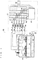
- FIG. 1 illustrates an example configuration of a radical gas generation system 500 including a power supply device (an electric discharge generator and a power supply device of electric discharge generator) according to an embodiment.
- FIG. 2 is an enlarged cross-sectional view of a configuration of a discharge cell 70 according to the present invention.
- FIG. 3 illustrates one embodiment by showing drive pulse cycles, pulse-width signal waveforms, and waveforms of alternating current voltages output to the discharge cells 70.
- the pulse cycles are for use in the driving of inverter elements 902 included in the n-phase inverter power supply device 9, which offers a means to output "n" output alternating current voltages.
- the radical generation system 500 will be described below with reference to FIGs. 1 , 2 , and 3 .
- the radical gas generation system 500 includes a radical gas generation apparatus 100, a process chamber apparatus 200, and one n-phase inverter power supply device 9 that can output the n-phase alternating current voltages, and a vacuum pump 300.
- n used to refer the n phase is equivalent to “n” representing the number of discharge cells 70 disposed in the radical gas generation apparatus 100.
- the radical gas generation system 500 is a film formation process system of remote plasma type in which the radical gas generation apparatus 100 that generates a radical gas G2 is located separately from the process chamber apparatus 200 that performs, for example, a film formation process in which the generated radical gas G2 is used.
- the bottom surface side of the radical gas generation apparatus 100 is in contact with the upper surface side of the process chamber apparatus 200.
- the inside of the radical gas generation apparatus 100 is connected to the inside of the process chamber apparatus 200 through an opening 102.
- a plurality of openings 102 are provided.
- the radical gas G2 is generated from a source gas G1 using the dielectric barrier discharge.
- the radical gas G2 is generated from part of the source gas G1 formed into a radical gas due to the dielectric barrier discharge.
- the radical gas generation apparatus 100 includes a plurality of discharge cells 70. Specifically, the discharge cells 70 are located on the bottom surface of the radical gas generation apparatus 100.
- each of the discharge cells 70 includes first electrode portions 1 and 2 and second electrode portions 5, 31, and 3.
- the first electrode portions 1 and 2 are opposed to the second electrode portion 5, 31, and 3 with a predetermined gap therebetween.
- a discharge space 40 is formed in which a dielectric barrier discharge occurs.
- At least one spacer 4 is located between the first electrode portions 1 and 2 and the second electrode portions 5, 31, and 3 such that the gap length (the distance between the first electrode portions 1 and 2 and the second electrode portions 5, 31, and 3 in FIG. 2 ) is kept equal across the discharge space 40.
- the first electrode portions 1 and 2 include a low voltage electrode (which can be regarded as a first electrode member) 1 and a first dielectric 2.
- the low voltage electrode 1 is at the ground potential and is located on the bottom surface of the radical gas generation apparatus 100. All of the discharge cells 70 share one low voltage electrode 1.
- the first dielectric 2 is formed on the low voltage electrode 1.
- the second electrode portions 5, 31, and 3 include a high voltage electrode block 5, a high voltage electrode (which can be regarded as a second electrode member) 31, and a second dielectric 3, respectively.
- the high voltage electrode 31 is formed on the second dielectric 3.
- the high voltage electrode block 5 is located on the high voltage electrode 31 so as to be connected thereto.
- the high voltage electrode block 5 is supplied with a high alternating current voltage.
- the high voltage electrode block 5 is electrically connected to the high voltage electrode 31, so that the high voltage is also applied to the high voltage electrode 31.
- the openings 102 that functions as orifices are provided in the individual discharge cells 70.
- Each of the openings 102 is formed so as to penetrate the first dielectric 2 and the low voltage electrode 1.
- the opening 102 is formed in the middle of the first dielectric 2.
- the inside of the radical gas generation apparatus 100 (specifically, the discharge space 40) is connected with the inside of the process chamber apparatus 200.
- the radical gas G2 generated in the discharge space 40 is output to the inside of the process chamber apparatus 200 through the opening 102.
- the opening 102 faces the treatment surface of a target object 202 placed in the process chamber apparatus 200.
- the individual discharge cell 70 has a disc-shaped outline or a coaxial conical outline in a plan view.
- the first dielectric 2 and the second dielectric 3 both have disc shapes or conical shapes and are located in parallel with each other or are located coaxially so as to be opposed to each other (the high voltage electrode 31 also has a disc shape or a conical shape).
- the discharge cell 70 is viewed from the above, the periphery of the first dielectric 2 coincides with the periphery of the second dielectric 3.
- the individual discharge cell 70 does not necessarily have a disc-shaped outline or a conical outline in a plan view and may have any shape as long as the same effects are produced.
- the outlines of the discharge cells 70 are of the same shape.
- the size of the outline of the discharge cell 70 in a plan view is determined by the diameter of the first dielectric 2 (and the diameter of the second dielectric 3).
- the n-phase inverter power supply device 9 includes a rectifier circuit 901, "n” inverter elements 902, “n” current-limiting reactors 903, “n” transformers 904, current detectors 906 that detect current flowing through the inverter elements 902, a gate circuit 905 that drives ON-OFF command signals from the individual inverter elements 902, and a control circuit 907 that controls the n-phase inverter power supply device 9.
- a commercial three-phase alternating current voltage is input to the rectifier circuit 901 of the n-phase inverter power supply device 9 (the three-phase alternating current voltage according to the illustration may be replaced with a single-phase alternating current voltage).
- the output voltage from the rectifier circuit 901 is rectified and converted into a direct current voltage.
- the direct current voltage is applied to a plurality of ("n") inverter elements 902 arranged in parallel with each other.
- the individual inverter element 902 includes two switching elements such as power transistors placed in series.
- the gate of the individual switching element receives, from the gate circuit 905, input of a signal alternating between ON and OFF.
- the signal is received, and then, the individual current-limiting reactor 903 receives input of an alternating current pulse voltage generated due to the switching between ON and OFF of the direct current voltage.
- the alternating current pulse voltage is input to the primary side of the individual transformer 904 via the individual current-limiting reactor 903.
- "n” transformers are coupled through delta connection.
- a primary voltage input to the individual transformer causes a secondary-side voltage of the individual transformer 904 to rise, and then, the resultant high voltage is output.
- Y-connection is formed, with one end of one of "n” transformers 904 and one end of another one of “n” transformers 904 being integral with each other and being at the same low voltage (LV).
- Alternating current high voltages (HV) of different phases are output to secondary-side terminals, each of which being another end of the individual transformer 904.
- the alternating current high voltages (HV) of different phases are applied to the discharge cells 70.
- the n-phase inverter power supply device 9 can output, to the radical gas generation apparatus 100 (specifically, to the discharge cells 70), a plurality of alternating current high voltages for discharging.
- the radical gas G2 is generated in the discharge space 40 due to the interaction between the source gas G1 passing through the discharge space 40 and the dielectric barrier discharge. That is to say, the radical gas G2, which is part of the source gas G1 formed into a radical gas due to the dielectric barrier discharge, is generated in the radical gas generation apparatus 100 using the dielectric barrier discharge.
- the source gas supply unit 101 supplies the radical gas generation apparatus 100 with the source gas G1, from which the radical gas G2 is to be derived.
- the source gas G1 supplied from the source gas supply unit 101 fills the radical gas generation apparatus 100.
- the fixed amount of the source gas G1 enters the discharge cells 70 from the outside thereof and flows through the discharge spaces 40.
- the radical gas G2 generated in the radical gas generation apparatus 100 is sprayed into the process chamber apparatus 200.
- the process chamber apparatus 200 performs a process, such as thin film formation, on the main surface of the target object 202 using the radical gas.
- the radical gas generation apparatus 100 is supplied with the source gas G1 which is a nitrogen gas.
- a nitrogen radical gas is generated, as the radical gas G2, from the nitrogen gas in the discharge cells 70 of the radical gas generation apparatus 100.
- the process chamber apparatus 200 accordingly forms a nitride film on the target object 202 using the nitrogen radical gas G2 sprayed from the radical gas generation apparatus 100.
- the radical gas generation apparatus 100 is supplied with the source gas G 1 which is an ozone gas or an oxygen gas.
- the source gas G 1 which is an ozone gas or an oxygen gas.
- an oxygen radical gas is generated, as the radical gas G2, from the ozone gas or the oxide gas in the discharge cells 70 of the radical gas generation apparatus 100.
- the process chamber apparatus 200 accordingly forms an oxide film on the target object 202 using the radical gas G2 sprayed from the radical gas generation apparatus 100.
- a gas outlet 203 that is to be connected to the vacuum pump 300.
- the gas is discharged through the vacuum pump 300, so that the pressure in the process chamber apparatus 200 is maintained at about several torrs to several tens of torrs (several kPa).
- the vacuum pump 300 produces a flow of gas from the radical gas generation apparatus 100 to the process chamber apparatus 200.
- the openings 102 function as orifices so that a pressure division is provided between the radical gas generation apparatus 100 and the process chamber apparatus 200.
- the outlines of the discharge cells 70 are of the same shape.
- the openings 102 formed in the discharge cells 70 have the same opening diameter.
- the gas flows equally through the discharge cells 70, so that the radical gas G2 is sprayed into the process chamber apparatus 200 at approximately the same speed.
- the speed of the radical gas G2 sprayed from the openings 102 of the discharge cells 40 is dependent on the source gas G1.
- the spray speed is low, it takes much time for the radical gas G2 to reach the target object 202 and part of the generated radical gas G2 probably disappears. Consequently, the target object 202 is exposed to the radical gas G2 in small concentrations (gas concentrations). This translates into a reduction in the efficiency of the process performed on the target object 202 through the use of the radical gas G2.
- each of the openings 102 be shaped in an orifice with a small opening diameter.
- each of the openings 102 has a small opening diameter
- the radical gas G2 is sprayed at a higher speed, and thus, the radical gas G2 is less likely to disappear.
- the area of the target object 202 exposed to the radical gas G2 is confined within narrow limits.
- each of the discharge cells 70 has the opening 102 formed therein, it is difficult to apply the radical gas G2 evenly to the target object 202 in the state in which the area exposed to the radical gas G2 is limited within narrow limits.
- the present invention therefore has the following configuration such that the spray speed of the radical gas G2 is kept high and equal among the discharge cells 70 and that the radical gas process is performed evenly over a wide area of the target object 202.
- the radical gas generation apparatus 100 When being exposed to the radical gas G2, the target object 202 is rotated along with the table 201 at a certain speed.
- the radical gas generation apparatus 100 includes the plurality of discharge cells 70. Each of the discharge cells 70 has the opening 102. The position of the individual opening 102 is fixed.
- the above-mentioned ON-OFF drive signals are represented by pulse signals a, b, c, d, ..., and n illustrated in FIG. 3 .
- the spray speed of the radical gas G2 is determined based mainly on the outside shapes of the dielectrics 2 and 3. As mentioned above, it is desirable that the outlines of the discharge cells 70 be of the same shape as illustrated in FIG. 2 such that the radical gas G2 is sprayed at the same speed. As long as the outside shapes of the dielectrics 2 and 3 are equal among the discharge cells 70, the radical gas G2 can be sprayed from the discharge cells 70 at the same speed, regardless of the differences in the outside shape of the high voltage electrode 31.
- the radical gas generation apparatus 100 fulfill the following conditions in order to drive the dielectric barrier discharge stably and to generate an excellent radical gas.
- the radical generation system that includes the power supply device and is for use in film formation has been described as one embodiment.
- the above-mentioned configuration is also applicable to other radical generators and power supply devices of electric discharge generators.
Landscapes
- Chemical & Material Sciences (AREA)
- Engineering & Computer Science (AREA)
- Physics & Mathematics (AREA)
- Plasma & Fusion (AREA)
- Analytical Chemistry (AREA)
- Mechanical Engineering (AREA)
- Chemical Kinetics & Catalysis (AREA)
- Materials Engineering (AREA)
- General Chemical & Material Sciences (AREA)
- Metallurgy (AREA)
- Organic Chemistry (AREA)
- Power Engineering (AREA)
- Electromagnetism (AREA)
- Spectroscopy & Molecular Physics (AREA)
- Inorganic Chemistry (AREA)
- Plasma Technology (AREA)
- Chemical Vapour Deposition (AREA)
Applications Claiming Priority (1)
| Application Number | Priority Date | Filing Date | Title |
|---|---|---|---|
| PCT/JP2014/078723 WO2016067380A1 (ja) | 2014-10-29 | 2014-10-29 | 放電発生器とその電源装置 |
Publications (3)
| Publication Number | Publication Date |
|---|---|
| EP3214906A1 true EP3214906A1 (de) | 2017-09-06 |
| EP3214906A4 EP3214906A4 (de) | 2018-03-21 |
| EP3214906B1 EP3214906B1 (de) | 2020-12-09 |
Family
ID=55856767
Family Applications (1)
| Application Number | Title | Priority Date | Filing Date |
|---|---|---|---|
| EP14904944.7A Active EP3214906B1 (de) | 2014-10-29 | 2014-10-29 | Generator für elektrische entladungen |
Country Status (7)
| Country | Link |
|---|---|
| US (1) | US11466366B2 (de) |
| EP (1) | EP3214906B1 (de) |
| JP (1) | JP6224266B2 (de) |
| KR (1) | KR101913985B1 (de) |
| CN (1) | CN107079575B (de) |
| TW (1) | TWI582822B (de) |
| WO (1) | WO2016067380A1 (de) |
Cited By (1)
| Publication number | Priority date | Publication date | Assignee | Title |
|---|---|---|---|---|
| EP4141141A1 (de) * | 2021-08-30 | 2023-03-01 | Creative Coatings Co., Ltd. | Filmbildende vorrichtung |
Families Citing this family (11)
| Publication number | Priority date | Publication date | Assignee | Title |
|---|---|---|---|---|
| WO2019049230A1 (ja) * | 2017-09-06 | 2019-03-14 | 東芝三菱電機産業システム株式会社 | 活性ガス生成装置 |
| WO2019138453A1 (ja) * | 2018-01-10 | 2019-07-18 | 東芝三菱電機産業システム株式会社 | 活性ガス生成装置及び成膜処理装置 |
| KR102024568B1 (ko) * | 2018-02-13 | 2019-09-24 | 한국기초과학지원연구원 | 환형 면방전 플라즈마 장치를 이용한 점상 식각 모듈 및 점상 식각 모듈의 식각 프로파일을 제어하는 방법 |
| US11532458B2 (en) * | 2018-05-30 | 2022-12-20 | Toshiba Mitsubishi-Electric Industrial Systems Corporation | Active gas generation apparatus |
| JP7085963B2 (ja) * | 2018-10-29 | 2022-06-17 | 東京エレクトロン株式会社 | プラズマ処理装置およびプラズマ処理方法 |
| WO2021033320A1 (ja) | 2019-08-22 | 2021-02-25 | 東芝三菱電機産業システム株式会社 | 活性ガス生成装置 |
| CN113170567B (zh) | 2019-11-12 | 2023-11-28 | 东芝三菱电机产业系统株式会社 | 活性气体生成装置 |
| US11839014B2 (en) * | 2019-11-27 | 2023-12-05 | Toshiba Mitsubishi-Electric Industrial Systems Corporation | Active gas generating apparatus |
| JP7377708B2 (ja) * | 2019-12-27 | 2023-11-10 | 日産自動車株式会社 | 電力変換器 |
| US20230411121A1 (en) * | 2022-06-16 | 2023-12-21 | Applied Materials, Inc. | Stackable plasma source for plasma processing |
| KR20250147340A (ko) * | 2024-04-04 | 2025-10-13 | 재단법인 멀티스케일 에너지시스템 연구단 | 고전도도 전도성 박막의 제조 방법 |
Family Cites Families (46)
| Publication number | Priority date | Publication date | Assignee | Title |
|---|---|---|---|---|
| JPS60232570A (ja) * | 1984-05-02 | 1985-11-19 | Ricoh Co Ltd | 放電器 |
| EP0831679B1 (de) | 1995-06-05 | 2008-10-01 | Musashino Kikai Co., Ltd. | Leistungsversorgung für multielektroden-entladung |
| US6082294A (en) * | 1996-06-07 | 2000-07-04 | Saint-Gobain Industrial Ceramics, Inc. | Method and apparatus for depositing diamond film |
| EP1073091A3 (de) | 1999-07-27 | 2004-10-06 | Matsushita Electric Works, Ltd. | Elektrode für Plasmaerzeugung, Anwendung dieser Elektrode in einem Plasmabehandlungsgerät, und Plasmabehandlung mittels dieses Gerätes |
| JP3366301B2 (ja) | 1999-11-10 | 2003-01-14 | 日本電気株式会社 | プラズマcvd装置 |
| WO2003019624A2 (en) * | 2001-08-27 | 2003-03-06 | University Of New Hampshire | Dielectric barrier discharge process for depositing silicon nitride film on substrates |
| US6764658B2 (en) * | 2002-01-08 | 2004-07-20 | Wisconsin Alumni Research Foundation | Plasma generator |
| JP3594947B2 (ja) | 2002-09-19 | 2004-12-02 | 東京エレクトロン株式会社 | 絶縁膜の形成方法、半導体装置の製造方法、基板処理装置 |
| JP4763974B2 (ja) * | 2003-05-27 | 2011-08-31 | パナソニック電工株式会社 | プラズマ処理装置及びプラズマ処理方法 |
| US7543546B2 (en) * | 2003-05-27 | 2009-06-09 | Matsushita Electric Works, Ltd. | Plasma processing apparatus, method for producing reaction vessel for plasma generation, and plasma processing method |
| US7767167B2 (en) * | 2003-07-28 | 2010-08-03 | Iono2X Engineering, L.L.C. | Dielectric barrier discharge cell with hermetically sealed electrodes, apparatus and method for the treatment of odor and volatile organic compound contaminants in air emissions, and for purifying gases and sterilizing surfaces |
| JP2005168275A (ja) * | 2003-11-14 | 2005-06-23 | Sekisui Chem Co Ltd | プラズマ処理装置 |
| US20050189278A1 (en) * | 2004-02-03 | 2005-09-01 | Takanori Iijima | Apparatus for decomposing organic matter with radical treatment method using electric discharge |
| JP4627532B2 (ja) * | 2004-09-29 | 2011-02-09 | 東芝三菱電機産業システム株式会社 | n相オゾン発生装置 |
| JP4932178B2 (ja) * | 2005-04-22 | 2012-05-16 | 立山マシン株式会社 | 多相交流プラズマ発生装置 |
| JP2006313674A (ja) | 2005-05-06 | 2006-11-16 | Sekisui Chem Co Ltd | プラズマ処理装置及びプラズマ処理方法 |
| DE112006002127A5 (de) | 2005-08-11 | 2008-07-03 | Fraunhofer-Gesellschaft zur Förderung der angewandten Forschung e.V. | Plasmaerzeugungsvorrichtung und Plasmaerzeugungsverfahren |
| JP4497323B2 (ja) | 2006-03-29 | 2010-07-07 | 三菱電機株式会社 | プラズマcvd装置 |
| US20070281106A1 (en) | 2006-05-30 | 2007-12-06 | Applied Materials, Inc. | Process chamber for dielectric gapfill |
| KR100737755B1 (ko) * | 2006-08-10 | 2007-07-10 | 세메스 주식회사 | 플라스마 생성유닛 및 이를 구비하는 기판처리장치와기판처리방법 |
| JP5168907B2 (ja) * | 2007-01-15 | 2013-03-27 | 東京エレクトロン株式会社 | プラズマ処理装置、プラズマ処理方法及び記憶媒体 |
| JP2008206372A (ja) | 2007-02-22 | 2008-09-04 | Nippon Reliance Kk | 交流電源装置 |
| US7453191B1 (en) * | 2007-07-06 | 2008-11-18 | Uion Co., Ltd. | Induction concentration remote atmospheric pressure plasma generating apparatus |
| GB2451489B (en) * | 2007-08-02 | 2009-07-29 | Peter Dean Christmas | Drum tuning device |
| US8857371B2 (en) * | 2007-08-31 | 2014-10-14 | Toshiba Mitsubishi-Electric Industrial Systems Corporation | Apparatus for generating dielectric barrier discharge gas |
| US20100081293A1 (en) * | 2008-10-01 | 2010-04-01 | Applied Materials, Inc. | Methods for forming silicon nitride based film or silicon carbon based film |
| JP5444961B2 (ja) | 2009-09-01 | 2014-03-19 | 東京エレクトロン株式会社 | 成膜装置及び成膜方法 |
| CN102770369B (zh) * | 2009-11-26 | 2014-11-26 | 东芝三菱电机产业系统株式会社 | 臭氧发生单元及臭氧气体供给系统 |
| CN102666372B (zh) * | 2009-11-26 | 2015-08-05 | 东芝三菱电机产业系统株式会社 | 臭氧气体供给系统 |
| JP5328685B2 (ja) * | 2010-01-28 | 2013-10-30 | 三菱電機株式会社 | プラズマ処理装置及びプラズマ処理方法 |
| JP5870279B2 (ja) * | 2010-07-21 | 2016-02-24 | パナソニックIpマネジメント株式会社 | プラズマ発生装置とラジカル生成方法、それらを用いた洗浄浄化装置および電器機器 |
| KR101160625B1 (ko) | 2010-09-20 | 2012-06-28 | 주식회사 뉴파워 프라즈마 | 상하 다중 분할 전극을 위한 다중 전원 공급원을 갖는 플라즈마 반응기 |
| KR101246170B1 (ko) * | 2011-01-13 | 2013-03-25 | 국제엘렉트릭코리아 주식회사 | 반도체 제조에 사용되는 분사부재 및 그것을 갖는 플라즈마 처리 장치 |
| JP5588974B2 (ja) * | 2011-03-24 | 2014-09-10 | 東芝三菱電機産業システム株式会社 | オゾンガス供給システム |
| US8980046B2 (en) * | 2011-04-11 | 2015-03-17 | Lam Research Corporation | Semiconductor processing system with source for decoupled ion and radical control |
| WO2012140747A1 (ja) * | 2011-04-13 | 2012-10-18 | 東芝三菱電機産業システム株式会社 | 窒素添加レス・オゾン発生ユニット及びオゾンガス供給システム |
| CN103766000B (zh) * | 2011-06-03 | 2018-04-10 | 株式会社和广武 | Cvd装置以及cvd膜的制造方法 |
| JP5694543B2 (ja) | 2011-09-08 | 2015-04-01 | 東芝三菱電機産業システム株式会社 | プラズマ発生装置、cvd装置およびプラズマ処理粒子生成装置 |
| JP2013084552A (ja) | 2011-09-29 | 2013-05-09 | Tokyo Electron Ltd | ラジカル選択装置及び基板処理装置 |
| US9295967B2 (en) * | 2011-10-04 | 2016-03-29 | Toshiba Mitsubishi-Electric Industrial Systems Corporation | Nitrogen-free ozone generating unit |
| US9396908B2 (en) * | 2011-11-22 | 2016-07-19 | Lam Research Corporation | Systems and methods for controlling a plasma edge region |
| EP2891625B1 (de) * | 2012-08-30 | 2017-01-04 | Toshiba Mitsubishi-Electric Industrial Systems Corporation | Ozongeneratorsystem |
| JP6207880B2 (ja) * | 2012-09-26 | 2017-10-04 | 東芝メモリ株式会社 | プラズマ処理装置およびプラズマ処理方法 |
| US9293926B2 (en) * | 2012-11-21 | 2016-03-22 | Lam Research Corporation | Plasma processing systems having multi-layer segmented electrodes and methods therefor |
| CN106797698B (zh) * | 2014-07-25 | 2019-11-15 | 东芝三菱电机产业系统株式会社 | 原子团气体产生系统 |
| JP6239483B2 (ja) * | 2014-10-29 | 2017-11-29 | 東芝三菱電機産業システム株式会社 | 窒素ラジカル生成システム |
-
2014
- 2014-10-29 CN CN201480083011.9A patent/CN107079575B/zh active Active
- 2014-10-29 US US15/521,645 patent/US11466366B2/en active Active
- 2014-10-29 JP JP2016556094A patent/JP6224266B2/ja active Active
- 2014-10-29 WO PCT/JP2014/078723 patent/WO2016067380A1/ja not_active Ceased
- 2014-10-29 KR KR1020177010742A patent/KR101913985B1/ko active Active
- 2014-10-29 EP EP14904944.7A patent/EP3214906B1/de active Active
-
2015
- 2015-01-09 TW TW104100694A patent/TWI582822B/zh active
Cited By (1)
| Publication number | Priority date | Publication date | Assignee | Title |
|---|---|---|---|---|
| EP4141141A1 (de) * | 2021-08-30 | 2023-03-01 | Creative Coatings Co., Ltd. | Filmbildende vorrichtung |
Also Published As
| Publication number | Publication date |
|---|---|
| US11466366B2 (en) | 2022-10-11 |
| JPWO2016067380A1 (ja) | 2017-04-27 |
| US20170241021A1 (en) | 2017-08-24 |
| KR101913985B1 (ko) | 2018-10-31 |
| CN107079575B (zh) | 2020-08-04 |
| TWI582822B (zh) | 2017-05-11 |
| CN107079575A (zh) | 2017-08-18 |
| EP3214906B1 (de) | 2020-12-09 |
| JP6224266B2 (ja) | 2017-11-01 |
| TW201616548A (zh) | 2016-05-01 |
| WO2016067380A1 (ja) | 2016-05-06 |
| KR20170058418A (ko) | 2017-05-26 |
| EP3214906A4 (de) | 2018-03-21 |
Similar Documents
| Publication | Publication Date | Title |
|---|---|---|
| US11466366B2 (en) | Electric discharge generator and power supply device of electric discharge generator | |
| US20260106116A1 (en) | Plasma processing method and plasma processing apparatus | |
| EP3193566A1 (de) | System zur erzeugung von radikalischem gas | |
| JP5808012B2 (ja) | プラズマ処理装置 | |
| JP2025131847A (ja) | 複数の埋込電極を有する基板支持体 | |
| KR102494482B1 (ko) | 반도체 공정들 및 장비를 위한 자기 유도 플라즈마 소스 | |
| KR102345906B1 (ko) | 정합기 및 플라즈마 처리 장치 | |
| US20130075390A1 (en) | Microwave processing apparatus and method for processing object to be processed | |
| EP2755453B1 (de) | Plasmagenerator und cvd-vorrichtung | |
| US20100065215A1 (en) | Plasma generating apparatus | |
| JP6339218B2 (ja) | 成膜装置へのガス噴射装置 | |
| US20150053645A1 (en) | Plasma processing apparatus and plasma processing method | |
| US20180233321A1 (en) | Ion directionality esc | |
| JP2023531370A (ja) | プラズマ生成装置及びその制御方法 | |
| US20250239435A1 (en) | Switching circuit for multilevel plasma impedance matching | |
| KR101607520B1 (ko) | 기판 처리 장치 및 기판 처리 방법 | |
| JP6454488B2 (ja) | プラズマ処理装置 | |
| KR101475502B1 (ko) | 다중방전관을 갖는 플라즈마 반응기 | |
| US20240339303A1 (en) | Substrate support and plasma processing apparatus | |
| JP2014150187A (ja) | プラズマ処理装置 |
Legal Events
| Date | Code | Title | Description |
|---|---|---|---|
| STAA | Information on the status of an ep patent application or granted ep patent |
Free format text: STATUS: THE INTERNATIONAL PUBLICATION HAS BEEN MADE |
|
| PUAI | Public reference made under article 153(3) epc to a published international application that has entered the european phase |
Free format text: ORIGINAL CODE: 0009012 |
|
| STAA | Information on the status of an ep patent application or granted ep patent |
Free format text: STATUS: REQUEST FOR EXAMINATION WAS MADE |
|
| 17P | Request for examination filed |
Effective date: 20170426 |
|
| AK | Designated contracting states |
Kind code of ref document: A1 Designated state(s): AL AT BE BG CH CY CZ DE DK EE ES FI FR GB GR HR HU IE IS IT LI LT LU LV MC MK MT NL NO PL PT RO RS SE SI SK SM TR |
|
| AX | Request for extension of the european patent |
Extension state: BA ME |
|
| DAX | Request for extension of the european patent (deleted) | ||
| A4 | Supplementary search report drawn up and despatched |
Effective date: 20180220 |
|
| RIC1 | Information provided on ipc code assigned before grant |
Ipc: H01L 21/31 20060101ALI20180214BHEP Ipc: H05H 1/46 20060101AFI20180214BHEP Ipc: H01J 37/32 20060101ALI20180214BHEP Ipc: C23C 16/50 20060101ALI20180214BHEP |
|
| R17P | Request for examination filed (corrected) |
Effective date: 20170426 |
|
| GRAP | Despatch of communication of intention to grant a patent |
Free format text: ORIGINAL CODE: EPIDOSNIGR1 |
|
| STAA | Information on the status of an ep patent application or granted ep patent |
Free format text: STATUS: GRANT OF PATENT IS INTENDED |
|
| INTG | Intention to grant announced |
Effective date: 20200716 |
|
| GRAS | Grant fee paid |
Free format text: ORIGINAL CODE: EPIDOSNIGR3 |
|
| GRAA | (expected) grant |
Free format text: ORIGINAL CODE: 0009210 |
|
| STAA | Information on the status of an ep patent application or granted ep patent |
Free format text: STATUS: THE PATENT HAS BEEN GRANTED |
|
| AK | Designated contracting states |
Kind code of ref document: B1 Designated state(s): AL AT BE BG CH CY CZ DE DK EE ES FI FR GB GR HR HU IE IS IT LI LT LU LV MC MK MT NL NO PL PT RO RS SE SI SK SM TR |
|
| REG | Reference to a national code |
Ref country code: GB Ref legal event code: FG4D |
|
| REG | Reference to a national code |
Ref country code: AT Ref legal event code: REF Ref document number: 1344691 Country of ref document: AT Kind code of ref document: T Effective date: 20201215 Ref country code: CH Ref legal event code: EP |
|
| REG | Reference to a national code |
Ref country code: DE Ref legal event code: R096 Ref document number: 602014073317 Country of ref document: DE |
|
| REG | Reference to a national code |
Ref country code: IE Ref legal event code: FG4D |
|
| PG25 | Lapsed in a contracting state [announced via postgrant information from national office to epo] |
Ref country code: GR Free format text: LAPSE BECAUSE OF FAILURE TO SUBMIT A TRANSLATION OF THE DESCRIPTION OR TO PAY THE FEE WITHIN THE PRESCRIBED TIME-LIMIT Effective date: 20210310 Ref country code: RS Free format text: LAPSE BECAUSE OF FAILURE TO SUBMIT A TRANSLATION OF THE DESCRIPTION OR TO PAY THE FEE WITHIN THE PRESCRIBED TIME-LIMIT Effective date: 20201209 Ref country code: FI Free format text: LAPSE BECAUSE OF FAILURE TO SUBMIT A TRANSLATION OF THE DESCRIPTION OR TO PAY THE FEE WITHIN THE PRESCRIBED TIME-LIMIT Effective date: 20201209 Ref country code: NO Free format text: LAPSE BECAUSE OF FAILURE TO SUBMIT A TRANSLATION OF THE DESCRIPTION OR TO PAY THE FEE WITHIN THE PRESCRIBED TIME-LIMIT Effective date: 20210309 |
|
| REG | Reference to a national code |
Ref country code: AT Ref legal event code: MK05 Ref document number: 1344691 Country of ref document: AT Kind code of ref document: T Effective date: 20201209 |
|
| PG25 | Lapsed in a contracting state [announced via postgrant information from national office to epo] |
Ref country code: BG Free format text: LAPSE BECAUSE OF FAILURE TO SUBMIT A TRANSLATION OF THE DESCRIPTION OR TO PAY THE FEE WITHIN THE PRESCRIBED TIME-LIMIT Effective date: 20210309 Ref country code: SE Free format text: LAPSE BECAUSE OF FAILURE TO SUBMIT A TRANSLATION OF THE DESCRIPTION OR TO PAY THE FEE WITHIN THE PRESCRIBED TIME-LIMIT Effective date: 20201209 Ref country code: LV Free format text: LAPSE BECAUSE OF FAILURE TO SUBMIT A TRANSLATION OF THE DESCRIPTION OR TO PAY THE FEE WITHIN THE PRESCRIBED TIME-LIMIT Effective date: 20201209 |
|
| REG | Reference to a national code |
Ref country code: NL Ref legal event code: MP Effective date: 20201209 |
|
| PG25 | Lapsed in a contracting state [announced via postgrant information from national office to epo] |
Ref country code: NL Free format text: LAPSE BECAUSE OF FAILURE TO SUBMIT A TRANSLATION OF THE DESCRIPTION OR TO PAY THE FEE WITHIN THE PRESCRIBED TIME-LIMIT Effective date: 20201209 Ref country code: HR Free format text: LAPSE BECAUSE OF FAILURE TO SUBMIT A TRANSLATION OF THE DESCRIPTION OR TO PAY THE FEE WITHIN THE PRESCRIBED TIME-LIMIT Effective date: 20201209 |
|
| REG | Reference to a national code |
Ref country code: LT Ref legal event code: MG9D |
|
| PG25 | Lapsed in a contracting state [announced via postgrant information from national office to epo] |
Ref country code: LT Free format text: LAPSE BECAUSE OF FAILURE TO SUBMIT A TRANSLATION OF THE DESCRIPTION OR TO PAY THE FEE WITHIN THE PRESCRIBED TIME-LIMIT Effective date: 20201209 Ref country code: PT Free format text: LAPSE BECAUSE OF FAILURE TO SUBMIT A TRANSLATION OF THE DESCRIPTION OR TO PAY THE FEE WITHIN THE PRESCRIBED TIME-LIMIT Effective date: 20210409 Ref country code: RO Free format text: LAPSE BECAUSE OF FAILURE TO SUBMIT A TRANSLATION OF THE DESCRIPTION OR TO PAY THE FEE WITHIN THE PRESCRIBED TIME-LIMIT Effective date: 20201209 Ref country code: SK Free format text: LAPSE BECAUSE OF FAILURE TO SUBMIT A TRANSLATION OF THE DESCRIPTION OR TO PAY THE FEE WITHIN THE PRESCRIBED TIME-LIMIT Effective date: 20201209 Ref country code: EE Free format text: LAPSE BECAUSE OF FAILURE TO SUBMIT A TRANSLATION OF THE DESCRIPTION OR TO PAY THE FEE WITHIN THE PRESCRIBED TIME-LIMIT Effective date: 20201209 Ref country code: CZ Free format text: LAPSE BECAUSE OF FAILURE TO SUBMIT A TRANSLATION OF THE DESCRIPTION OR TO PAY THE FEE WITHIN THE PRESCRIBED TIME-LIMIT Effective date: 20201209 Ref country code: SM Free format text: LAPSE BECAUSE OF FAILURE TO SUBMIT A TRANSLATION OF THE DESCRIPTION OR TO PAY THE FEE WITHIN THE PRESCRIBED TIME-LIMIT Effective date: 20201209 |
|
| PG25 | Lapsed in a contracting state [announced via postgrant information from national office to epo] |
Ref country code: PL Free format text: LAPSE BECAUSE OF FAILURE TO SUBMIT A TRANSLATION OF THE DESCRIPTION OR TO PAY THE FEE WITHIN THE PRESCRIBED TIME-LIMIT Effective date: 20201209 Ref country code: AT Free format text: LAPSE BECAUSE OF FAILURE TO SUBMIT A TRANSLATION OF THE DESCRIPTION OR TO PAY THE FEE WITHIN THE PRESCRIBED TIME-LIMIT Effective date: 20201209 |
|
| REG | Reference to a national code |
Ref country code: DE Ref legal event code: R097 Ref document number: 602014073317 Country of ref document: DE |
|
| PG25 | Lapsed in a contracting state [announced via postgrant information from national office to epo] |
Ref country code: IS Free format text: LAPSE BECAUSE OF FAILURE TO SUBMIT A TRANSLATION OF THE DESCRIPTION OR TO PAY THE FEE WITHIN THE PRESCRIBED TIME-LIMIT Effective date: 20210409 |
|
| PLBE | No opposition filed within time limit |
Free format text: ORIGINAL CODE: 0009261 |
|
| STAA | Information on the status of an ep patent application or granted ep patent |
Free format text: STATUS: NO OPPOSITION FILED WITHIN TIME LIMIT |
|
| PG25 | Lapsed in a contracting state [announced via postgrant information from national office to epo] |
Ref country code: IT Free format text: LAPSE BECAUSE OF FAILURE TO SUBMIT A TRANSLATION OF THE DESCRIPTION OR TO PAY THE FEE WITHIN THE PRESCRIBED TIME-LIMIT Effective date: 20201209 Ref country code: AL Free format text: LAPSE BECAUSE OF FAILURE TO SUBMIT A TRANSLATION OF THE DESCRIPTION OR TO PAY THE FEE WITHIN THE PRESCRIBED TIME-LIMIT Effective date: 20201209 |
|
| 26N | No opposition filed |
Effective date: 20210910 |
|
| PG25 | Lapsed in a contracting state [announced via postgrant information from national office to epo] |
Ref country code: DK Free format text: LAPSE BECAUSE OF FAILURE TO SUBMIT A TRANSLATION OF THE DESCRIPTION OR TO PAY THE FEE WITHIN THE PRESCRIBED TIME-LIMIT Effective date: 20201209 Ref country code: SI Free format text: LAPSE BECAUSE OF FAILURE TO SUBMIT A TRANSLATION OF THE DESCRIPTION OR TO PAY THE FEE WITHIN THE PRESCRIBED TIME-LIMIT Effective date: 20201209 |
|
| PG25 | Lapsed in a contracting state [announced via postgrant information from national office to epo] |
Ref country code: ES Free format text: LAPSE BECAUSE OF FAILURE TO SUBMIT A TRANSLATION OF THE DESCRIPTION OR TO PAY THE FEE WITHIN THE PRESCRIBED TIME-LIMIT Effective date: 20201209 |
|
| REG | Reference to a national code |
Ref country code: CH Ref legal event code: PL |
|
| PG25 | Lapsed in a contracting state [announced via postgrant information from national office to epo] |
Ref country code: IS Free format text: LAPSE BECAUSE OF FAILURE TO SUBMIT A TRANSLATION OF THE DESCRIPTION OR TO PAY THE FEE WITHIN THE PRESCRIBED TIME-LIMIT Effective date: 20210409 |
|
| GBPC | Gb: european patent ceased through non-payment of renewal fee |
Effective date: 20211029 |
|
| PG25 | Lapsed in a contracting state [announced via postgrant information from national office to epo] |
Ref country code: MC Free format text: LAPSE BECAUSE OF FAILURE TO SUBMIT A TRANSLATION OF THE DESCRIPTION OR TO PAY THE FEE WITHIN THE PRESCRIBED TIME-LIMIT Effective date: 20201209 |
|
| PG25 | Lapsed in a contracting state [announced via postgrant information from national office to epo] |
Ref country code: LU Free format text: LAPSE BECAUSE OF NON-PAYMENT OF DUE FEES Effective date: 20211029 Ref country code: GB Free format text: LAPSE BECAUSE OF NON-PAYMENT OF DUE FEES Effective date: 20211029 |
|
| PG25 | Lapsed in a contracting state [announced via postgrant information from national office to epo] |
Ref country code: LI Free format text: LAPSE BECAUSE OF NON-PAYMENT OF DUE FEES Effective date: 20211031 Ref country code: CH Free format text: LAPSE BECAUSE OF NON-PAYMENT OF DUE FEES Effective date: 20211031 |
|
| PG25 | Lapsed in a contracting state [announced via postgrant information from national office to epo] |
Ref country code: FR Free format text: LAPSE BECAUSE OF NON-PAYMENT OF DUE FEES Effective date: 20211031 |
|
| PG25 | Lapsed in a contracting state [announced via postgrant information from national office to epo] |
Ref country code: IE Free format text: LAPSE BECAUSE OF NON-PAYMENT OF DUE FEES Effective date: 20211029 |
|
| PG25 | Lapsed in a contracting state [announced via postgrant information from national office to epo] |
Ref country code: HU Free format text: LAPSE BECAUSE OF FAILURE TO SUBMIT A TRANSLATION OF THE DESCRIPTION OR TO PAY THE FEE WITHIN THE PRESCRIBED TIME-LIMIT; INVALID AB INITIO Effective date: 20141029 |
|
| PG25 | Lapsed in a contracting state [announced via postgrant information from national office to epo] |
Ref country code: CY Free format text: LAPSE BECAUSE OF FAILURE TO SUBMIT A TRANSLATION OF THE DESCRIPTION OR TO PAY THE FEE WITHIN THE PRESCRIBED TIME-LIMIT Effective date: 20201209 |
|
| PG25 | Lapsed in a contracting state [announced via postgrant information from national office to epo] |
Ref country code: MK Free format text: LAPSE BECAUSE OF FAILURE TO SUBMIT A TRANSLATION OF THE DESCRIPTION OR TO PAY THE FEE WITHIN THE PRESCRIBED TIME-LIMIT Effective date: 20201209 |
|
| PG25 | Lapsed in a contracting state [announced via postgrant information from national office to epo] |
Ref country code: MT Free format text: LAPSE BECAUSE OF FAILURE TO SUBMIT A TRANSLATION OF THE DESCRIPTION OR TO PAY THE FEE WITHIN THE PRESCRIBED TIME-LIMIT Effective date: 20201209 |
|
| PGFP | Annual fee paid to national office [announced via postgrant information from national office to epo] |
Ref country code: BE Payment date: 20250917 Year of fee payment: 12 |
|
| PG25 | Lapsed in a contracting state [announced via postgrant information from national office to epo] |
Ref country code: TR Free format text: LAPSE BECAUSE OF FAILURE TO SUBMIT A TRANSLATION OF THE DESCRIPTION OR TO PAY THE FEE WITHIN THE PRESCRIBED TIME-LIMIT Effective date: 20201209 |
|
| PGFP | Annual fee paid to national office [announced via postgrant information from national office to epo] |
Ref country code: DE Payment date: 20250902 Year of fee payment: 12 |