EP3217291B1 - Systèmes de circuits intégrés - Google Patents
Systèmes de circuits intégrés Download PDFInfo
- Publication number
- EP3217291B1 EP3217291B1 EP16160037.4A EP16160037A EP3217291B1 EP 3217291 B1 EP3217291 B1 EP 3217291B1 EP 16160037 A EP16160037 A EP 16160037A EP 3217291 B1 EP3217291 B1 EP 3217291B1
- Authority
- EP
- European Patent Office
- Prior art keywords
- chip
- output
- signal
- circuitry
- low voltage
- Prior art date
- Legal status (The legal status is an assumption and is not a legal conclusion. Google has not performed a legal analysis and makes no representation as to the accuracy of the status listed.)
- Active
Links
Images




Classifications
-
- H—ELECTRICITY
- H04—ELECTRIC COMMUNICATION TECHNIQUE
- H04B—TRANSMISSION
- H04B14/00—Transmission systems not characterised by the medium used for transmission
- H04B14/02—Transmission systems not characterised by the medium used for transmission characterised by the use of pulse modulation
- H04B14/04—Transmission systems not characterised by the medium used for transmission characterised by the use of pulse modulation using pulse code modulation
- H04B14/042—Special circuits, e.g. comparators
-
- G—PHYSICS
- G06—COMPUTING OR CALCULATING; COUNTING
- G06F—ELECTRIC DIGITAL DATA PROCESSING
- G06F13/00—Interconnection of, or transfer of information or other signals between, memories, input/output devices or central processing units
- G06F13/38—Information transfer, e.g. on bus
- G06F13/40—Bus structure
- G06F13/4063—Device-to-bus coupling
- G06F13/4068—Electrical coupling
- G06F13/4072—Drivers or receivers
-
- G—PHYSICS
- G06—COMPUTING OR CALCULATING; COUNTING
- G06F—ELECTRIC DIGITAL DATA PROCESSING
- G06F13/00—Interconnection of, or transfer of information or other signals between, memories, input/output devices or central processing units
- G06F13/38—Information transfer, e.g. on bus
- G06F13/40—Bus structure
- G06F13/4063—Device-to-bus coupling
- G06F13/4068—Electrical coupling
- G06F13/4086—Bus impedance matching, e.g. termination
-
- H—ELECTRICITY
- H04—ELECTRIC COMMUNICATION TECHNIQUE
- H04L—TRANSMISSION OF DIGITAL INFORMATION, e.g. TELEGRAPHIC COMMUNICATION
- H04L47/00—Traffic control in data switching networks
- H04L47/50—Queue scheduling
- H04L47/62—Queue scheduling characterised by scheduling criteria
- H04L47/6295—Queue scheduling characterised by scheduling criteria using multiple queues, one for each individual QoS, connection, flow or priority
-
- H—ELECTRICITY
- H10—SEMICONDUCTOR DEVICES; ELECTRIC SOLID-STATE DEVICES NOT OTHERWISE PROVIDED FOR
- H10W—GENERIC PACKAGES, INTERCONNECTIONS, CONNECTORS OR OTHER CONSTRUCTIONAL DETAILS OF DEVICES COVERED BY CLASS H10
- H10W90/00—Package configurations
-
- H—ELECTRICITY
- H10—SEMICONDUCTOR DEVICES; ELECTRIC SOLID-STATE DEVICES NOT OTHERWISE PROVIDED FOR
- H10W—GENERIC PACKAGES, INTERCONNECTIONS, CONNECTORS OR OTHER CONSTRUCTIONAL DETAILS OF DEVICES COVERED BY CLASS H10
- H10W70/00—Package substrates; Interposers; Redistribution layers [RDL]
- H10W70/60—Insulating or insulated package substrates; Interposers; Redistribution layers
- H10W70/62—Insulating or insulated package substrates; Interposers; Redistribution layers characterised by their interconnections
- H10W70/63—Vias, e.g. via plugs
-
- H—ELECTRICITY
- H10—SEMICONDUCTOR DEVICES; ELECTRIC SOLID-STATE DEVICES NOT OTHERWISE PROVIDED FOR
- H10W—GENERIC PACKAGES, INTERCONNECTIONS, CONNECTORS OR OTHER CONSTRUCTIONAL DETAILS OF DEVICES COVERED BY CLASS H10
- H10W90/00—Package configurations
- H10W90/701—Package configurations characterised by the relative positions of pads or connectors relative to package parts
- H10W90/721—Package configurations characterised by the relative positions of pads or connectors relative to package parts of bump connectors
- H10W90/724—Package configurations characterised by the relative positions of pads or connectors relative to package parts of bump connectors between a chip and a stacked insulating package substrate, interposer or RDL
-
- Y—GENERAL TAGGING OF NEW TECHNOLOGICAL DEVELOPMENTS; GENERAL TAGGING OF CROSS-SECTIONAL TECHNOLOGIES SPANNING OVER SEVERAL SECTIONS OF THE IPC; TECHNICAL SUBJECTS COVERED BY FORMER USPC CROSS-REFERENCE ART COLLECTIONS [XRACs] AND DIGESTS
- Y02—TECHNOLOGIES OR APPLICATIONS FOR MITIGATION OR ADAPTATION AGAINST CLIMATE CHANGE
- Y02D—CLIMATE CHANGE MITIGATION TECHNOLOGIES IN INFORMATION AND COMMUNICATION TECHNOLOGIES [ICT], I.E. INFORMATION AND COMMUNICATION TECHNOLOGIES AIMING AT THE REDUCTION OF THEIR OWN ENERGY USE
- Y02D10/00—Energy efficient computing, e.g. low power processors, power management or thermal management
Definitions
- the present invention relates to integrated circuitry systems, and in particular to multi-chip circuitry systems.
- the present invention relates in particular to systems for enabling a high-speed (high data rate) connection, link or interface between integrated circuits such as may be provided on separate IC chips. That is, different sets of integrated circuitry may be disposed on different IC chips, and the present invention considers how to transmit a signal from one such chip to another. Such chips are examples of integrated circuits, and as such the present invention considers how to transmit a signal from one such integrated circuit to another.
- Figure 1 presents a schematic diagram of a previously-considered circuitry system 1.
- Circuitry system 1 comprises a chip A 2 and a chip B 4.
- Chip A 2 comprises an analogue-to-digital convertor (ADC) unit 6, a digital-to-analogue convertor (DAC) unit 8, a transmission interface 10 and a reception interface 12.
- Chip B 4 comprises a first digital unit 14, a second digital unit 16, a reception interface 18 and a transmission interface 20.
- the ADC unit 6 is configured and connected to output a digital signal via the transmission interface 10 and the reception interface 18 to the first digital unit 14.
- the second digital unit 16 is configured and connected to output a digital signal via the transmission interface 20 and the reception interface 12 to the DAC unit 8.
- the transmission and reception interfaces 10, 12, 18 and 20 and the connections therebetween may be referred to collectively as a chip-to-chip interface 22.
- Such a system provides a link between a chip A having ADC and/or DAC circuitry and a chip B having digital circuitry.
- the circuitry in the two chips may be any sets of circuitry which need to send a signal one to the other, such as two sets of digital circuitry.
- the link (and the interface 22) may be in both directions, but it may also be in either direction, i.e. from chip A to chip B (only) or vice versa.
- the link between the mixed-signal circuitry (DAC or ADC) and the digital circuitry may be readily implemented on-chip, when both sets of circuitry are provided on the same chip.
- Examples of ADC circuitry to which the present invention may be applied are found in EP2211468 , the entire contents of which are incorporated herein by reference.
- Examples of DAC circuitry to which the present invention may be applied are found in EP2849345 , the entire contents of which are incorporated herein by reference.
- the ADC unit 6 may for example be an 8b 128 Ms/s ADC outputting data at around 1 Tb/s (e.g. 1024b @ 1GHz).
- the DAC unit 8 e.g. adopting the circuitry of EP2849345 , may also handle (input) data at around 1 Tb/s.
- Figure 2 is another schematic diagram of circuitry system 1, indicating that it may be implemented as flip chips inside a flip-chip package.
- System 1 of Figure 2 comprises a flip-chip package 30, the flip-chip package 30 comprising a substrate 32 on which the chips (implemented as flip chips) A 2 and B 4 are mounted, and a protective lid 34.
- the flip chips 2 and 4 may have for example "normal” bumps (typically at 150 ⁇ m pitch) or "micro bumps” (typically at 50 ⁇ m pitch).
- the link or interface 22 may be implemented as connections in the package 30, or more particularly via the substrate 32. It should be noted that in the example of Figure 2 it is assumed that the chip A 2 has multiple ADC units 6, each referred to as an ADC channel. For example, chip A 2 may have up to 16 such channels each requiring a 1 Tb/s connection to chip B 4. Each channel may have only 32 bumps available, which limits how the interface 22 may be implemented.
- the high and low voltage-reference terminals of the first IC chip may be respectively connected to the high and low voltage-reference terminals of the second IC chip so that the high and low voltage-reference sources of the first IC chip are respectively connected to the high and low voltage-reference terminals of the second IC chip as voltage-reference sources therefor. That is, the voltage-reference sources of the first IC chip may maintain respective voltage levels at the high and low voltage-reference terminals of the first IC chip, and control the high and low voltage-reference terminals of the second IC chip.
- the high and low voltage-reference terminals of the second IC chip may be separate (i.e. electrically, or conductively) from any voltage-reference sources of the second IC chip itself, so that they are effectively supplied or powered from the first IC chip. That is, currents which circulate via the high and low voltage-reference terminals of the second IC chip are supplied from the first IC chip (via its voltage-reference sources), rather than from the second IC chip. That is, the currents which circulate via the high and low voltage-reference terminals of the second IC chip may be independent of currents generated by voltage-reference sources (e.g. a power supply unit) of the second IC chip.
- voltage-reference sources e.g. a power supply unit
- current paths passing through the potential-divider arrangement may be closed in the sense that currents caused to flow along those paths are both sourced and sunk in the first IC chip, rather than in the second IC chip.
- Current paths (all current paths) which pass through said potential-divider arrangement may extend from the high voltage-reference source of the first IC chip to the low voltage-reference source of the first IC chip, forming closed current loops supplied by the first IC chip.
- the high and low voltage-reference terminals of the second IC chip may be considered high and low voltage-reference "input" terminals.
- the input terminal of the second IC chip may be connected to an input terminal (having high input impedance) of an input buffer of the second IC chip, via which an internal signal of the second IC chip may be generated based upon the output signal received at the input terminal of the second IC chip from the first IC chip.
- Such an input buffer may afford separation between currents which circulate via the high and low voltage-reference terminals of the second IC chip and any currents generated by voltage-reference sources (e.g. a power supply unit) of the second IC chip.
- Such a system has the advantage that signals can be transmitted between such chips whilst only requiring one signal-line connection per signal.
- the connections between the voltage-reference terminals and the potential-divider arrangement allow the circulation of currents across the interface between the two chips (supplied from the first IC chip), enabling data-independent power consumption as discussed in more detail below.
- the output-signal unit may be a signal buffer, for example comprising or being a CMOS inverter.
- CMOS inverters enable low power operation.
- the output-signal unit and potential-divider arrangement may be configured such that the resistance they present (together) between the high and low voltage-reference sources is substantially the same when the output signal has a logic low value as when it has a logic high value. This has the advantage of enabling data-independent power consumption, since the same current is drawn from a power supply unit in the first IC chip irrespective of the signal level (logic high or logic low).
- the output-signal unit may be configured to present a first on resistance between the high voltage-reference source and the output terminal when the output signal has the logic high value and to present a second on resistance between the low voltage-reference source and the output terminal when the output signal has the logic low value, with the first and second on resistances being substantially the same as one another.
- the potential-divider arrangement may be configured to present a first potential-divider resistance between the high voltage-reference source and the input terminal and to present a second potential-divider resistance between the low voltage-reference source and the input terminal, with the first and second potential-divider resistances being substantially the same as one another.
- the output-signal unit may be configured to output the output signal as a switched logic level signal such as a digital (e.g. data) signal, which signal may be configured to switch between the voltage levels of the high and low voltage-reference sources.
- a switched logic level signal such as a digital (e.g. data) signal
- analogue signals such as sinusoidal (raised cosine) signals may also be considered to switch between logic high and logic low values, and the present disclosure will be considered accordingly.
- the output signal may be a single-ended signal, requiring only one signal line. This helps keep the number of signal lines required to transmit multiple such signals relatively low.
- the system may be configured or configurable such that the output terminal of the first IC chip is connected to the input terminal of the second IC chip via a transmission line connection (i.e. having a transmission line).
- a transmission line connection may comprise a transmission line, serving as such a signal line.
- the input impedance of such a transmission line may be equal to the on-resistances of the output-signal unit.
- the first and second potential-divider resistances may each have a resistance twice the input impedance of the transmission line.
- the system may be configured or configurable such that the output signal is transmitted from the first IC chip to the second IC chip via only the single connection between the output terminal of the first IC chip and the input terminal of the second IC chip.
- the first IC chip may comprise analogue-to-digital converter circuitry, the output signal being a digital signal output from the analogue-to-digital converter circuitry, and the second IC chip may comprise digital circuitry configured to operate in dependence upon that digital signal.
- the first IC chip may comprise digital circuitry, the output signal being a digital signal output from the digital circuitry, and the second IC chip may comprise digital-to-analogue converter circuitry configured to operate in dependence upon that digital signal. Both possibilities may be provided in parallel (i.e. with two signal lines), or on a time-share basis with the input and output terminals being configurable as output and input terminals, respectively, and connectable to the relevant circuitry blocks in their chips.
- the present disclosure will be interpreted to extend to such chips which may be configured (i.e. that are configurable) in this manner.
- the first and second IC chips may be configured or configurable such that they have a plurality of said output terminals and input terminals.
- the first and second IC chips may be configured or configurable such that: each said output terminal is connected to receive a corresponding output signal from a corresponding output-signal unit of the first IC chip; each said output-signal unit is connected between said high and low voltage-reference sources of the first IC chip; and each said input terminal is connected in a potential-divider arrangement between said high and low voltage-reference terminals of the second IC chip, wherein each said output terminal of the first IC chip is connected to a corresponding said input terminal of the second IC chip for transmission of its corresponding output signal from the first IC chip to the second IC chip.
- multiple signals may be transmitted with the overall link sharing the same high and low voltage-reference terminals.
- the system may be referred to as a flip-chip package, wherein said first and second IC chips are flip chips of the flip-chip package.
- mixed-signal circuitry (involving analogue-to-digital or digital-to-analogue conversion), comprising the aforementioned circuitry.
- the present disclosure extends to method aspects corresponding to the apparatus aspects.
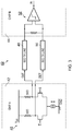
- FIG. 3 is a schematic diagram of a previously-considered circuitry system 40, in which a known serial de-serial (SERDES) transmitter is adopted.
- SERDES serial de-serial
- System 40 comprises chips A 42 and B 44 corresponding respectively to chips A and B in Figures 1 and 2 .
- circuitry units DAC, ADC, and digital, etc.
- FIG. 3 the circuitry shown in Figure 3 could be considered to correspond to such a link or interface.
- Chip A 42 comprises (SERDES) transmission circuitry 46, configured to take differential input signals S and /S and to output corresponding output signals OUT and /OUT as indicated.
- these signals OUT and /OUT are transmitted via 50 ⁇ (ideally, lossless) transmission lines 48 and 50 to corresponding reception circuitry 52 in chip B 44, which employs a comparator buffer to arrive at input signal IN which is input to a circuitry unit (not shown) in chip B 44 operable dependent upon that input signal.
- the link of circuitry system 40 is differential, requiring two signal lines or wires (transmission lines 48 and 50) per signal transmitted between chips A42 B44.
- the link or interface is a constant current link, assuming the transmission of switched logic level signals (such as digital signals, which could be data, control or clock signals), it is a relatively high-power link given for example the power dissipated in the transmitter.
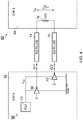
- Figure 4 is a schematic diagram of previously-considered circuitry system 60 which corresponds to the circuitry system 40 of Figure 3 but which employs a lower-power transmitter.
- Circuitry system 60 comprises chips A 62 and B 64, corresponding respectively to chips A and B in Figures 1 to 3 .
- Chip A 62 comprises transmission circuitry 66, configured to take differential input signals S and /S and to output corresponding output signals OUT and /OUT as indicated.
- the transmission circuitry 66 comprises first and second buffers 68 and 70 (for signals S and /S, respectively) connected to receive power from the explicitly shown power supply unit (PSU) 72.
- PSU power supply unit
- the receiver circuitry in chip B 64 comprises, in this example, a 100 ⁇ resistor 78 between the two transmission lines 74 and 76 at the input to chip B 64, generating a VDD/2 swing in the input signal voltage V IN as indicated.
- the transmitted signals OUT and /OUT are switched logic level signals such as digital data signals as mentioned above, which switch in logic level between logic high (or VDD) and logic low (or ground, GND).
- the interface circuitry of Figure 4 may be configured to operate at relatively low power, given the CMOS buffers 68 and 70 at the transmission side and the potential to lower VDD to for example around 0.2V. Also, such an interface enables constant current draw from the PSU 72, but, as in Figure 3 , requires two signal lines (transmission lines 74 and 76) per signal transmitted between chips A 62 and B 64.
- Figures 5A and 5B present schematic diagrams of a circuitry system 80 embodying the present invention. It will become apparent that Figures 5A and 5B present the same circuitry system 80 but under different signal conditions.
- Circuitry system 80 comprises chips A 82 and B 84 which correspond respectively to chips A and B in Figures 1 to 4 .
- the chip-to-chip interface or link of circuitry system 80 is considered advantageous when compared to those of systems 40 and 60.
- Chip A 82 comprises transmission circuitry 86, configured to take single-ended signal S and to output a corresponding single-ended output signal OUT as indicated.
- the transmission circuitry 86 comprises a buffer 88 connected to receive power from the PSU 90. That is, buffer 88 is connected between logic high (VDD) and logic low (ground, or GND) voltage reference sources provided by the PSU 90.
- the chip A 82 also comprises a high voltage-reference terminal 92, a low voltage-reference terminal 94 and an output terminal 96.
- the output of the buffer 88 is connected to the output terminal 96 so as to provide the output signal OUT thereto.
- the PSU 90 is connected to the high and low voltage-reference terminals 92 and 94 so as to connect the high and low voltage-reference sources VDD and GND thereto, respectively.
- the chip B 84 has a potential-divider arrangement 100 serving as reception circuitry, the potential-divider arrangement 100 having a first potential-divider resistance 102 and a second potential-divider resistance 104.
- the chip B 84 also comprises a high voltage-reference terminal 106, a low voltage-reference terminal 108 and an input terminal 110.
- the first potential-divider resistance 102 is connected between the high voltage-reference terminal 106 and the input terminal 110, and the second potential-divider resistance 104 is connected between the low voltage-reference terminal 108 and the input terminal 110, thus forming the potential-divider arrangement 100.
- the input signal IN is provided at the input terminal 110.
- the circuitry system 80 also comprises a signal line 112 connected between the output terminal 96 of the chip A82 and the input terminal 110 of the chip B84, a signal line 114 connected between the high voltage-reference terminal 92 of chip A and the high voltage-reference terminal 106 of chip B, and a signal line 116 connected between the low voltage-reference terminal 94 of chip A and the low voltage-reference terminal 108 of chip B.
- the signal line 112 is implemented as a transmission line, in the present running example as a 50 ⁇ (ideally, lossless) transmission line.
- the signal lines 114 and 116 serve as high and low voltage-reference connections between the chips A and B.
- signal lines 114 and 116 may be implemented as reference planes to be low impedance (inductance) compared to the signal tracks (e.g. signal line 112) to prevent coupling between multiple such signal tracks (e.g. data wires) due to common impedance.
- the presence of such multiple signal tracks is explored in Figure 6 below.
- Figure 5B is labelled in the same way as Figure 5A for ease of comparison.
- the resistances 102 and 104 form part of current paths which pass through terminals 92/94/96 and ultimately through PSU 90. Those paths are independent (conductively separate) from any current paths of chip B 84 for which their currents are sourced and sunk in chip B 84.
- VDD 1V and that the two resistors 102 and 104 are 100 ⁇ resistors as indicated.
- the link or interface is single-ended i.e. only a single signal line 112 (transmission line) per signal link is needed rather than two lines or wires per link as in the differential link as in the differential link of Figures 3 and 4 .
- a single-wire link can be accommodated by designing sufficient separation/shielding between adjacent signal-wire links.
- Such links may be relatively short, e.g. under 5mm as between flip chips in a flip chip package.
- the circuitry system 80 assumes the allowance of varying VDD and GND currents, and currents circulating back to PSU 90.
- VDD and GND currents there is 5 mA DC ⁇ 2.5 mA AC current flowing in the VDD and GND planes 114 and 116 per link.
- These reference planes 114 and 116 could be dedicated "link" reference planes separate from the actual VDD and GND planes of one or both of chips A 82 and B 84.
- the receiving side experiences a voltage swing between 1 ⁇ 4 and 3 ⁇ 4 VDD based on the selections of component values in those Figures, and this signal could be fed into a buffer comparator (not shown) along with a reference 1 ⁇ 2 VDD signal (not shown) supplied (in common to the or all of the signal links) from chip A 82 to chip B 84.
- the swing between 1 ⁇ 4 and 3 ⁇ 4 VDD is indicated by way of the graphs for the input voltage V IN of the input signal IN in Figures 5A and 5B .
- the circuitry system 80 of Figures 5A and 5B has various advantages. For example, it has half the power consumption per signal link and half the number of wires per signal link.
- VDD 1 V
- this equates to 240 mA for the overall 1Tb/s link and power consumption of 240 mW.
- VDD could be reduced to for example 0.2 V leading to 1.5mA/wire and 48mA and 9mW for the overall 1Tb/s link. This equates to around 10 fJ/bit/sec, which is very low power.
- the range of the present link is considered suitable for an approximately 3mm link between chip A 82 and B 84, for example in the case that they are implemented as flip chips in a flip-chip package in line with Figure 2 .
- FIG. 6 is a schematic diagram of a circuitry system 120, embodying the present invention. It will be appreciated that the circuitry system 120 is closely similar to the circuitry system 80 of Figures 5A and 5B , and is provided simply to demonstrate that multiple signal links may be provided together, sharing the same reference planes as mentioned above. Accordingly, where possible, elements of circuitry system 120 are denoted in the same manner as their counterparts in circuitry system 80, and duplicate description is omitted.
- Circuitry system 120 of Figure 6 comprises chips A 122 and B 124 corresponding respectively to chips A 82 and B 84 of circuitry system 80 of Figures 5A and 5B .
- circuitry system 120 The main difference between circuitry system 120 and circuitry system 80 is that a plurality (X, where X is an integer) of signals S1 to SX are transmitted as corresponding output signals OUT1 to OUTX via corresponding buffers 88 1 to 88 X .
- corresponding output terminals 96 1 to 96 X signal lines (transmission lines) 112 1 to 112x, input terminals 110 1 to 110 X and potential-divider arrangements 100 1 to 100 X (having corresponding first resistances 102 1 to 102 X and second resistances 104 1 to 104 X ) are provided, so as to input corresponding input signals IN1 to INX to chip B 124.
- Note that (only) one set of reference planes 114 and 116 is provided in common to the plurality of signal links, i.e. that no proliferation in reference planes is needed.
- the 100 ⁇ resistors in Figures 5A and 5B could be implemented as transistors or (e.g. poly, diffusion) resistors.
- An advantage of using transistors is that the link could be designed as a programmable bi-directional link, with an appropriate network of transistors and control signals. Additionally, by using a network of transistors, R ON calibration would also be possible.
- the IC chips disclosed herein may be considered to be examples of integrated circuits, for example with a plurality provided together as a multi-chip module or as a hybrid integrated circuit or as a system-in-a-package. It will also be appreciated that the present invention could in some embodiments be applied within a single IC chip.
- the first and second IC chips mentioned above could be referred to as first and second integrated-circuit portions, for example both provided on the same IC chip, and the terminals could be referred to as circuitry nodes. The above disclosure may be understood accordingly.
- circuitry disclosed herein could be described as a DAC or ADC or mixed-signal system.
- the IC chips disclosed herein may be flip chips.
- the present invention extends to integrated circuitry and IC chips as mentioned above, flip-chip packages, circuit boards comprising such IC chips or flip-chip packages, and communication networks (for example, internet fiber-optic networks and wireless networks) and network equipment of such networks, comprising such circuit boards.
Landscapes
- Engineering & Computer Science (AREA)
- General Engineering & Computer Science (AREA)
- Theoretical Computer Science (AREA)
- Computer Hardware Design (AREA)
- Physics & Mathematics (AREA)
- General Physics & Mathematics (AREA)
- Computer Networks & Wireless Communication (AREA)
- Signal Processing (AREA)
- Semiconductor Integrated Circuits (AREA)
- Logic Circuits (AREA)
Claims (15)
- Système de montage de circuits (80) comprenant des première et seconde puces de circuit intégré, IC, (82, 84), le système étant configuré de sorte que :la première puce de circuit IC (82) présente une borne de sortie (96) connectée de manière à recevoir un signal de sortie numérique en provenance d'une unité de signal de sortie (88) de la première puce de circuit IC, l'unité de signal de sortie étant connectée entre des sources de référence de haute tension et de basse tension de la première puce de circuit IC, les sources de référence de haute tension et de basse tension étant connectées à des bornes de référence de haute tension et de basse tension respectives (92, 94) de la première puce de circuit IC ; etla seconde puce de circuit IC (84) présente une borne d'entrée (110) connectée dans un agencement de diviseur de tension (102, 104) entre des bornes de référence de haute tension et de basse tension (106, 108) de la seconde puce de circuit IC ;dans lequel :les bornes de référence de haute tension et de basse tension (92, 94) de la première puce de circuit IC sont respectivement connectées aux bornes de référence de haute tension et de basse tension (106, 108) de la seconde puce de circuit IC ;la borne de sortie (96) de la première puce de circuit IC est connectée à la borne d'entrée (110) de la seconde puce de circuit IC en vue d'une transmission du signal de sortie, de la première puce de circuit IC à la seconde puce de circuit IC ;l'agencement de diviseur de tension (102, 104) est configuré de manière à comprendre une première résistance de diviseur de tension (102) qui s'étend de la borne de référence de haute tension (106) de la seconde puce de circuit IC à la borne d'entrée (110) de la seconde puce de circuit IC, et une seconde résistance de diviseur de tension (104) qui s'étend de la borne de référence de basse tension (108) de la seconde puce de circuit IC à la borne d'entrée (110) de la seconde puce de circuit IC ; caractérisé en ce que :
l'agencement de diviseur de tension est configuré de sorte que :pour une première valeur logique du signal de sortie, un premier courant tiré de la source de référence de haute tension de la première puce de circuit IC (82) passe par la seconde puce de circuit IC (84), par l'intermédiaire des bornes de référence de haute tension (92, 106), et à travers la première résistance de diviseur de tension (102), le premier courant se divisant ensuite en une première partie et une seconde partie, où la première partie du premier courant revient à la première puce de circuit IC (82) par l'intermédiaire des bornes de sortie et d'entrée (110, 96), et la seconde partie du premier courant revient à la première puce de circuit IC (82) par l'intermédiaire des bornes de référence de basse tension (108, 94) ; etpour une seconde valeur logique du signal de sortie, un second courant tiré de la source de référence de haute tension de la première puce de circuit IC (92) se divise en une première partie et une seconde partie au sein de la première puce de circuit IC (82), où la première partie du second courant passe par la seconde puce de circuit IC (84) par l'intermédiaire des bornes de référence de haute tension (92, 106) et à travers la première résistance de diviseur de tension (102), et la seconde partie du second courant passe par la seconde puce de circuit IC (84) par l'intermédiaire des bornes d'entrée et de sortie (96, 110), et où une somme des première et seconde parties du second courant revient à la première puce de circuit IC (92) par l'intermédiaire des bornes de référence de basse tension (108, 94). - Système de montage de circuits selon la revendication 1, dans lequel :l'unité de signal de sortie (88) est un tampon de signal, comprenant ou étant facultativement un onduleur ; et/oules bornes de référence de haute tension et de basse tension (92, 94) de la première puce de circuit IC sont respectivement connectées aux bornes de référence de haute tension et de basse tension (106, 108) de la seconde puce de circuit IC, de sorte que les sources de référence de haute tension et de basse tension de la première puce de circuit IC sont respectivement connectées aux bornes de référence de haute tension et de basse tension de la seconde puce de circuit IC, en tant que des sources de référence de tension pour celle-ci ; et/oudes trajets de courant qui passent par ledit agencement de diviseur de tension s'étendent de la source de référence de haute tension de la première puce de circuit IC à la source de référence de basse tension de la première puce de circuit IC.
- Système de montage de circuits selon la revendication 1 ou 2, dans lequel l'unité de signal de sortie (88) et l'agencement de diviseur de tension (102, 104) sont configurés de sorte que la résistance qu'ils présentent entre les sources de référence de haute tension et de basse tension lorsque le signal de sortie présente une valeur d'état logique 0, et la résistance qu'ils présentent entre les sources de référence de haute tension et de basse tension lorsque le signal de sortie présente une valeur d'état logique 1, sont sensiblement identiques l'une à l'autre.
- Système de montage de circuits selon l'une quelconque des revendications précédentes, dans lequel l'unité de signal de sortie (88) est configurée de manière à présenter une première résistance à l'état passant entre la source de référence de haute tension et la borne de sortie, lorsque le signal de sortie présente la valeur d'état logique 1, et à présenter une seconde résistance à l'état passant entre la source de référence de basse tension et la borne de sortie, lorsque le signal de sortie présente la valeur d'état logique 0, et dans lequel lesdites première et seconde résistances à l'état passant sont sensiblement identiques l'une à l'autre.
- Système de montage de circuits selon l'une quelconque des revendications précédentes, dans lequel lesdites première et seconde résistances de diviseur de tension (102, 104) sont sensiblement identiques l'une à l'autre.
- Système de montage de circuits selon l'une quelconque des revendications précédentes, dans lequel l'unité de signal de sortie (88) est configurée de manière à fournir en sortie le signal de sortie sous la forme d'un signal de niveau logique commuté, tel qu'un signal numérique, lequel signal est facultativement configuré de manière à commuter entre les tensions des sources de référence de haute tension et de basse tension.
- Système de montage de circuits selon l'une quelconque des revendications précédentes, dans lequel le signal de sortie est un signal asymétrique.
- Système de montage de circuits selon l'une quelconque des revendications précédentes, configuré de sorte que la borne de sortie de la première puce de circuit IC est connectée à la borne d'entrée de la seconde puce de circuit IC par l'intermédiaire d'une connexion de ligne de transmission (112).
- Système de montage de circuits selon la revendication 8, dans lequel :l'impédance d'entrée de la ligne de transmission (112) est égale aux résistances à l'état passant de l'unité de signal de sortie (88) lorsque le signal de sortie présente une valeur d'état logique 0, et lorsque le signal de sortie présente une valeur d'état logique 1 ; et/oules première et seconde résistances de diviseur de tension (102, 104) présentent chacune une résistance deux fois supérieure à l'impédance d'entrée de la ligne de transmission.
- Système de montage de circuits selon l'une quelconque des revendications précédentes, configuré de sorte que le signal de sortie est transmis de la première puce de circuit IC (82) à la seconde puce de circuit IC (84) uniquement par l'intermédiaire de la connexion unique entre la borne de sortie de la première puce de circuit IC et la borne d'entrée de la seconde puce de circuit IC.
- Système de montage de circuits selon l'une quelconque des revendications précédentes, dans lequel :la première puce de circuit IC comprend un montage de circuits de conversion analogique-numérique, le signal de sortie est un signal numérique fourni en sortie à partir du montage de circuits de conversion analogique-numérique, et la seconde puce de circuit IC comprend un montage de circuits numérique configuré de manière à fonctionner en fonction de ce signal numérique ; oula première puce de circuit IC comprend un montage de circuits numérique, le signal de sortie est un signal numérique fourni en sortie à partir du montage de circuits numérique, et la seconde puce de circuit IC comprend un montage de circuits de convertisseur numérique-analogique configuré de manière à fonctionner en fonction de ce signal numérique ; oula première puce de circuit IC comprend un montage de circuits numérique, le signal de sortie est un signal numérique fourni en sortie à partir de ce montage de circuits numérique, et la seconde puce de circuit IC comprend un montage de circuits numérique configuré de manière à fonctionner en fonction de ce signal numérique.
- Système de montage de circuits selon l'une quelconque des revendications précédentes, dans lequel les première et seconde puces de circuit intégré sont configurées de sorte qu'elles présentent une pluralité desdites bornes de sortie et bornes d'entrée.
- Système de montage de circuits selon la revendication 12, dans lequel les première et seconde puces de circuit intégré sont configurées de sorte que :chaque dite borne de sortie est connectée de manière à recevoir un signal de sortie correspondant en provenance d'une unité de signal de sortie correspondante de la première puce de circuit IC ;chaque dite unité de signal de sortie est connectée entre lesdites sources de référence de haute tension et de basse tension de la première puce de circuit IC ; etchaque dite borne d'entrée est connectée dans un agencement de diviseur de tension correspondant entre lesdites bornes de référence de haute tension et de basse tension de la seconde puce de circuit IC ;dans lequel chaque dite borne de sortie de la première puce de circuit IC est connectée à une dite borne d'entrée correspondante de la seconde puce de circuit IC, en vue d'une transmission de son signal de sortie correspondant, de la première puce de circuit IC à la seconde puce de circuit IC.
- Système de montage de circuits selon l'une quelconque des revendications précédentes, lequel est ou comprend un boîtier à puces retournées, dans lequel lesdites première et seconde puces de circuit IC sont des puces retournées du boîtier à puces retournées.
- Montage de circuits à signaux mixtes, comprenant le système de montage de circuits selon l'une quelconque des revendications précédentes.
Priority Applications (2)
| Application Number | Priority Date | Filing Date | Title |
|---|---|---|---|
| EP16160037.4A EP3217291B1 (fr) | 2016-03-11 | 2016-03-11 | Systèmes de circuits intégrés |
| US15/456,289 US10090936B2 (en) | 2016-03-11 | 2017-03-10 | Integrated circuitry systems |
Applications Claiming Priority (1)
| Application Number | Priority Date | Filing Date | Title |
|---|---|---|---|
| EP16160037.4A EP3217291B1 (fr) | 2016-03-11 | 2016-03-11 | Systèmes de circuits intégrés |
Publications (2)
| Publication Number | Publication Date |
|---|---|
| EP3217291A1 EP3217291A1 (fr) | 2017-09-13 |
| EP3217291B1 true EP3217291B1 (fr) | 2020-06-17 |
Family
ID=55587063
Family Applications (1)
| Application Number | Title | Priority Date | Filing Date |
|---|---|---|---|
| EP16160037.4A Active EP3217291B1 (fr) | 2016-03-11 | 2016-03-11 | Systèmes de circuits intégrés |
Country Status (2)
| Country | Link |
|---|---|
| US (1) | US10090936B2 (fr) |
| EP (1) | EP3217291B1 (fr) |
Families Citing this family (1)
| Publication number | Priority date | Publication date | Assignee | Title |
|---|---|---|---|---|
| EP3457567B1 (fr) | 2017-09-15 | 2020-11-25 | Socionext Inc. | Alignement de phase |
Family Cites Families (21)
| Publication number | Priority date | Publication date | Assignee | Title |
|---|---|---|---|---|
| US5864584A (en) * | 1995-02-13 | 1999-01-26 | International Business Machines Corporation | Circuitry for allowing two drivers to communicate with two receivers using one transmission line |
| US6184717B1 (en) * | 1998-12-09 | 2001-02-06 | Nortel Networks Limited | Digital signal transmitter and receiver using source based reference logic levels |
| US6453422B1 (en) * | 1999-12-23 | 2002-09-17 | Intel Corporation | Reference voltage distribution for multiload i/o systems |
| US6304098B1 (en) * | 2000-03-14 | 2001-10-16 | Sun Microsystems, Inc. | Method and apparatus for reducing noise in communication channels having a shared reference signal |
| US7127003B2 (en) * | 2002-09-23 | 2006-10-24 | Rambus Inc. | Method and apparatus for communicating information using different signaling types |
| JP4593915B2 (ja) * | 2002-12-31 | 2010-12-08 | 三星電子株式会社 | 同時両方向入出力回路及び方法 |
| US7230449B2 (en) * | 2005-02-11 | 2007-06-12 | International Business Machines Corporation | Data receiver with a programmable reference voltage to optimize timing jitter |
| US7242339B1 (en) * | 2006-01-17 | 2007-07-10 | International Business Machines Corporation | Programmable reference voltage generator |
| US8130821B2 (en) * | 2006-05-18 | 2012-03-06 | Oracle America, Inc. | Equalization in capacitively coupled communication links |
| KR101533120B1 (ko) * | 2006-12-14 | 2015-07-01 | 램버스 인코포레이티드 | 멀티 다이 메모리 디바이스 |
| US8975752B2 (en) * | 2008-01-09 | 2015-03-10 | Oracle America, Inc. | Multiple access over proximity communication |
| US8259461B2 (en) * | 2008-11-25 | 2012-09-04 | Micron Technology, Inc. | Apparatus for bypassing faulty connections |
| EP2485399B1 (fr) | 2009-01-26 | 2013-11-13 | Fujitsu Semiconductor Limited | Échantillonnage |
| US8605397B2 (en) * | 2009-05-07 | 2013-12-10 | Rambus Inc. | Configurable, power supply voltage referenced single-ended signaling with ESD protection |
| WO2011025557A1 (fr) * | 2009-08-31 | 2011-03-03 | Rambus Inc. | Transfert de tension d'alimentation de signal dans un système de transmission de données |
| WO2011049693A2 (fr) * | 2009-10-20 | 2011-04-28 | Rambus Inc. | Signalisation asymétrique avec circulation parallèle des courants de transmission de signal et de retour de signal |
| US8767531B2 (en) * | 2010-10-27 | 2014-07-01 | International Business Machines Corporation | Dynamic fault detection and repair in a data communications mechanism |
| US9182782B2 (en) * | 2011-09-22 | 2015-11-10 | Oracle International Corporation | Synchronizing timing of communication between integrated circuits |
| US8898504B2 (en) * | 2011-12-14 | 2014-11-25 | International Business Machines Corporation | Parallel data communications mechanism having reduced power continuously calibrated lines |
| TWI490842B (zh) * | 2012-10-29 | 2015-07-01 | Dazzo Technology Corp | 顯示裝置、驅動晶片組及其運作方法 |
| EP2849345B1 (fr) | 2013-09-12 | 2020-11-04 | Socionext Inc. | Circuits et procédés à utiliser dans des circuits à signaux mixtes |
-
2016
- 2016-03-11 EP EP16160037.4A patent/EP3217291B1/fr active Active
-
2017
- 2017-03-10 US US15/456,289 patent/US10090936B2/en active Active
Non-Patent Citations (1)
| Title |
|---|
| None * |
Also Published As
| Publication number | Publication date |
|---|---|
| US10090936B2 (en) | 2018-10-02 |
| US20170264375A1 (en) | 2017-09-14 |
| EP3217291A1 (fr) | 2017-09-13 |
Similar Documents
| Publication | Publication Date | Title |
|---|---|---|
| US11126581B2 (en) | Reconfigurable transmitter | |
| US11283654B2 (en) | Multilevel driver for high speed chip-to-chip communications | |
| Dehlaghi et al. | A 0.3 pJ/bit 20 Gb/s/wire parallel interface for die-to-die communication | |
| Kim et al. | 3.5 A 16-to-40Gb/s quarter-rate NRZ/PAM4 dual-mode transmitter in 14nm CMOS | |
| Kim et al. | A 112Gb/s PAM-4 transmitter with 3-Tap FFE in 10nm CMOS | |
| US11398934B1 (en) | Ultra-high-speed PAM-N CMOS inverter serial link | |
| US8605397B2 (en) | Configurable, power supply voltage referenced single-ended signaling with ESD protection | |
| Song et al. | A 0.47–0.66 pJ/bit, 4.8–8 Gb/s I/O transceiver in 65 nm CMOS | |
| Kennedy et al. | A 3.6-Gb/s point-to-point heterogeneous-voltage-capable DRAM interface for capacity-scalable memory subsystems | |
| Lu et al. | Design and analysis of energy-efficient reconfigurable pre-emphasis voltage-mode transmitters | |
| Steffan et al. | 6.4 A 64Gb/s PAM-4 transmitter with 4-Tap FFE and 2.26 pJ/b energy efficiency in 28nm CMOS FDSOI | |
| Bassi et al. | 3.6 A 45Gb/s PAM-4 transmitter delivering 1.3 Vppd output swing with 1V supply in 28nm CMOS FDSOI | |
| CN112019176A (zh) | H桥集成激光驱动器 | |
| US9698735B1 (en) | Low voltage differential signal receiver with fully integrated AC coupling and bias latching | |
| US11449453B2 (en) | Multi-package system using configurable input/output interface circuits for single-ended intra-package communication and differential inter-package communication | |
| Hsueh et al. | 26.4 A 25.6 Gb/s differential and DDR4/GDDR5 dual-mode transmitter with digital clock calibration in 22nm CMOS | |
| Pan et al. | A full-duplex line driver for gigabit ethernet with rail-to-rail class-ab output stage in 28 nm cmos | |
| Kim et al. | A 16/32 Gb/s dual-mode NRZ/PAM4 voltage-mode transmitter with 2-tap FFE | |
| EP3217291B1 (fr) | Systèmes de circuits intégrés | |
| Dehlaghi et al. | A 20 Gb/s 0.3 pJ/b single-ended die-to-die transceiver in 28 nm-SOI CMOS | |
| Amarasinghe | A Single-ended Simultaneously Bidirectional Transceiver for Ultra-short Reach Die to Die Links | |
| Wary et al. | Current-mode triline transceiver for coded differential signaling across on-chip global interconnects | |
| Diniz | JESD204B vs. serial LVDS interface considerations for wideband data converter applications | |
| Lu et al. | A 10Gb/s 10mW 2-tap reconfigurable pre-emphasis transmitter in 65nm LP CMOS |
Legal Events
| Date | Code | Title | Description |
|---|---|---|---|
| PUAI | Public reference made under article 153(3) epc to a published international application that has entered the european phase |
Free format text: ORIGINAL CODE: 0009012 |
|
| STAA | Information on the status of an ep patent application or granted ep patent |
Free format text: STATUS: THE APPLICATION HAS BEEN PUBLISHED |
|
| AK | Designated contracting states |
Kind code of ref document: A1 Designated state(s): AL AT BE BG CH CY CZ DE DK EE ES FI FR GB GR HR HU IE IS IT LI LT LU LV MC MK MT NL NO PL PT RO RS SE SI SK SM TR |
|
| AX | Request for extension of the european patent |
Extension state: BA ME |
|
| STAA | Information on the status of an ep patent application or granted ep patent |
Free format text: STATUS: REQUEST FOR EXAMINATION WAS MADE |
|
| 17P | Request for examination filed |
Effective date: 20180209 |
|
| RBV | Designated contracting states (corrected) |
Designated state(s): AL AT BE BG CH CY CZ DE DK EE ES FI FR GB GR HR HU IE IS IT LI LT LU LV MC MK MT NL NO PL PT RO RS SE SI SK SM TR |
|
| GRAP | Despatch of communication of intention to grant a patent |
Free format text: ORIGINAL CODE: EPIDOSNIGR1 |
|
| STAA | Information on the status of an ep patent application or granted ep patent |
Free format text: STATUS: GRANT OF PATENT IS INTENDED |
|
| RIC1 | Information provided on ipc code assigned before grant |
Ipc: G06F 13/40 20060101AFI20191213BHEP |
|
| INTG | Intention to grant announced |
Effective date: 20200110 |
|
| GRAS | Grant fee paid |
Free format text: ORIGINAL CODE: EPIDOSNIGR3 |
|
| GRAA | (expected) grant |
Free format text: ORIGINAL CODE: 0009210 |
|
| STAA | Information on the status of an ep patent application or granted ep patent |
Free format text: STATUS: THE PATENT HAS BEEN GRANTED |
|
| AK | Designated contracting states |
Kind code of ref document: B1 Designated state(s): AL AT BE BG CH CY CZ DE DK EE ES FI FR GB GR HR HU IE IS IT LI LT LU LV MC MK MT NL NO PL PT RO RS SE SI SK SM TR |
|
| REG | Reference to a national code |
Ref country code: GB Ref legal event code: FG4D |
|
| REG | Reference to a national code |
Ref country code: CH Ref legal event code: EP |
|
| REG | Reference to a national code |
Ref country code: IE Ref legal event code: FG4D |
|
| REG | Reference to a national code |
Ref country code: DE Ref legal event code: R096 Ref document number: 602016038074 Country of ref document: DE |
|
| REG | Reference to a national code |
Ref country code: AT Ref legal event code: REF Ref document number: 1282196 Country of ref document: AT Kind code of ref document: T Effective date: 20200715 |
|
| PG25 | Lapsed in a contracting state [announced via postgrant information from national office to epo] |
Ref country code: LT Free format text: LAPSE BECAUSE OF FAILURE TO SUBMIT A TRANSLATION OF THE DESCRIPTION OR TO PAY THE FEE WITHIN THE PRESCRIBED TIME-LIMIT Effective date: 20200617 Ref country code: SE Free format text: LAPSE BECAUSE OF FAILURE TO SUBMIT A TRANSLATION OF THE DESCRIPTION OR TO PAY THE FEE WITHIN THE PRESCRIBED TIME-LIMIT Effective date: 20200617 Ref country code: GR Free format text: LAPSE BECAUSE OF FAILURE TO SUBMIT A TRANSLATION OF THE DESCRIPTION OR TO PAY THE FEE WITHIN THE PRESCRIBED TIME-LIMIT Effective date: 20200918 Ref country code: NO Free format text: LAPSE BECAUSE OF FAILURE TO SUBMIT A TRANSLATION OF THE DESCRIPTION OR TO PAY THE FEE WITHIN THE PRESCRIBED TIME-LIMIT Effective date: 20200917 Ref country code: FI Free format text: LAPSE BECAUSE OF FAILURE TO SUBMIT A TRANSLATION OF THE DESCRIPTION OR TO PAY THE FEE WITHIN THE PRESCRIBED TIME-LIMIT Effective date: 20200617 |
|
| REG | Reference to a national code |
Ref country code: LT Ref legal event code: MG4D |
|
| REG | Reference to a national code |
Ref country code: NL Ref legal event code: MP Effective date: 20200617 |
|
| PG25 | Lapsed in a contracting state [announced via postgrant information from national office to epo] |
Ref country code: LV Free format text: LAPSE BECAUSE OF FAILURE TO SUBMIT A TRANSLATION OF THE DESCRIPTION OR TO PAY THE FEE WITHIN THE PRESCRIBED TIME-LIMIT Effective date: 20200617 Ref country code: HR Free format text: LAPSE BECAUSE OF FAILURE TO SUBMIT A TRANSLATION OF THE DESCRIPTION OR TO PAY THE FEE WITHIN THE PRESCRIBED TIME-LIMIT Effective date: 20200617 Ref country code: BG Free format text: LAPSE BECAUSE OF FAILURE TO SUBMIT A TRANSLATION OF THE DESCRIPTION OR TO PAY THE FEE WITHIN THE PRESCRIBED TIME-LIMIT Effective date: 20200917 Ref country code: RS Free format text: LAPSE BECAUSE OF FAILURE TO SUBMIT A TRANSLATION OF THE DESCRIPTION OR TO PAY THE FEE WITHIN THE PRESCRIBED TIME-LIMIT Effective date: 20200617 |
|
| REG | Reference to a national code |
Ref country code: AT Ref legal event code: MK05 Ref document number: 1282196 Country of ref document: AT Kind code of ref document: T Effective date: 20200617 |
|
| PG25 | Lapsed in a contracting state [announced via postgrant information from national office to epo] |
Ref country code: NL Free format text: LAPSE BECAUSE OF FAILURE TO SUBMIT A TRANSLATION OF THE DESCRIPTION OR TO PAY THE FEE WITHIN THE PRESCRIBED TIME-LIMIT Effective date: 20200617 Ref country code: AL Free format text: LAPSE BECAUSE OF FAILURE TO SUBMIT A TRANSLATION OF THE DESCRIPTION OR TO PAY THE FEE WITHIN THE PRESCRIBED TIME-LIMIT Effective date: 20200617 |
|
| REG | Reference to a national code |
Ref country code: DE Ref legal event code: R082 Ref document number: 602016038074 Country of ref document: DE Representative=s name: HL KEMPNER PATENTANWAELTE, SOLICITORS (ENGLAND, DE Ref country code: DE Ref legal event code: R082 Ref document number: 602016038074 Country of ref document: DE Representative=s name: HL KEMPNER PATENTANWALT, RECHTSANWALT, SOLICIT, DE Ref country code: DE Ref legal event code: R082 Ref document number: 602016038074 Country of ref document: DE Representative=s name: HL KEMPNER PARTG MBB, DE |
|
| PG25 | Lapsed in a contracting state [announced via postgrant information from national office to epo] |
Ref country code: CZ Free format text: LAPSE BECAUSE OF FAILURE TO SUBMIT A TRANSLATION OF THE DESCRIPTION OR TO PAY THE FEE WITHIN THE PRESCRIBED TIME-LIMIT Effective date: 20200617 Ref country code: RO Free format text: LAPSE BECAUSE OF FAILURE TO SUBMIT A TRANSLATION OF THE DESCRIPTION OR TO PAY THE FEE WITHIN THE PRESCRIBED TIME-LIMIT Effective date: 20200617 Ref country code: IT Free format text: LAPSE BECAUSE OF FAILURE TO SUBMIT A TRANSLATION OF THE DESCRIPTION OR TO PAY THE FEE WITHIN THE PRESCRIBED TIME-LIMIT Effective date: 20200617 Ref country code: PT Free format text: LAPSE BECAUSE OF FAILURE TO SUBMIT A TRANSLATION OF THE DESCRIPTION OR TO PAY THE FEE WITHIN THE PRESCRIBED TIME-LIMIT Effective date: 20201019 Ref country code: AT Free format text: LAPSE BECAUSE OF FAILURE TO SUBMIT A TRANSLATION OF THE DESCRIPTION OR TO PAY THE FEE WITHIN THE PRESCRIBED TIME-LIMIT Effective date: 20200617 Ref country code: ES Free format text: LAPSE BECAUSE OF FAILURE TO SUBMIT A TRANSLATION OF THE DESCRIPTION OR TO PAY THE FEE WITHIN THE PRESCRIBED TIME-LIMIT Effective date: 20200617 Ref country code: EE Free format text: LAPSE BECAUSE OF FAILURE TO SUBMIT A TRANSLATION OF THE DESCRIPTION OR TO PAY THE FEE WITHIN THE PRESCRIBED TIME-LIMIT Effective date: 20200617 Ref country code: SM Free format text: LAPSE BECAUSE OF FAILURE TO SUBMIT A TRANSLATION OF THE DESCRIPTION OR TO PAY THE FEE WITHIN THE PRESCRIBED TIME-LIMIT Effective date: 20200617 |
|
| PG25 | Lapsed in a contracting state [announced via postgrant information from national office to epo] |
Ref country code: PL Free format text: LAPSE BECAUSE OF FAILURE TO SUBMIT A TRANSLATION OF THE DESCRIPTION OR TO PAY THE FEE WITHIN THE PRESCRIBED TIME-LIMIT Effective date: 20200617 Ref country code: SK Free format text: LAPSE BECAUSE OF FAILURE TO SUBMIT A TRANSLATION OF THE DESCRIPTION OR TO PAY THE FEE WITHIN THE PRESCRIBED TIME-LIMIT Effective date: 20200617 Ref country code: IS Free format text: LAPSE BECAUSE OF FAILURE TO SUBMIT A TRANSLATION OF THE DESCRIPTION OR TO PAY THE FEE WITHIN THE PRESCRIBED TIME-LIMIT Effective date: 20201017 |
|
| REG | Reference to a national code |
Ref country code: DE Ref legal event code: R097 Ref document number: 602016038074 Country of ref document: DE |
|
| PLBE | No opposition filed within time limit |
Free format text: ORIGINAL CODE: 0009261 |
|
| STAA | Information on the status of an ep patent application or granted ep patent |
Free format text: STATUS: NO OPPOSITION FILED WITHIN TIME LIMIT |
|
| PG25 | Lapsed in a contracting state [announced via postgrant information from national office to epo] |
Ref country code: DK Free format text: LAPSE BECAUSE OF FAILURE TO SUBMIT A TRANSLATION OF THE DESCRIPTION OR TO PAY THE FEE WITHIN THE PRESCRIBED TIME-LIMIT Effective date: 20200617 |
|
| 26N | No opposition filed |
Effective date: 20210318 |
|
| PG25 | Lapsed in a contracting state [announced via postgrant information from national office to epo] |
Ref country code: SI Free format text: LAPSE BECAUSE OF FAILURE TO SUBMIT A TRANSLATION OF THE DESCRIPTION OR TO PAY THE FEE WITHIN THE PRESCRIBED TIME-LIMIT Effective date: 20200617 |
|
| PG25 | Lapsed in a contracting state [announced via postgrant information from national office to epo] |
Ref country code: MC Free format text: LAPSE BECAUSE OF FAILURE TO SUBMIT A TRANSLATION OF THE DESCRIPTION OR TO PAY THE FEE WITHIN THE PRESCRIBED TIME-LIMIT Effective date: 20200617 |
|
| REG | Reference to a national code |
Ref country code: CH Ref legal event code: PL |
|
| REG | Reference to a national code |
Ref country code: BE Ref legal event code: MM Effective date: 20210331 |
|
| PG25 | Lapsed in a contracting state [announced via postgrant information from national office to epo] |
Ref country code: IE Free format text: LAPSE BECAUSE OF NON-PAYMENT OF DUE FEES Effective date: 20210311 Ref country code: LI Free format text: LAPSE BECAUSE OF NON-PAYMENT OF DUE FEES Effective date: 20210331 Ref country code: LU Free format text: LAPSE BECAUSE OF NON-PAYMENT OF DUE FEES Effective date: 20210311 Ref country code: CH Free format text: LAPSE BECAUSE OF NON-PAYMENT OF DUE FEES Effective date: 20210331 |
|
| PG25 | Lapsed in a contracting state [announced via postgrant information from national office to epo] |
Ref country code: BE Free format text: LAPSE BECAUSE OF NON-PAYMENT OF DUE FEES Effective date: 20210331 |
|
| PG25 | Lapsed in a contracting state [announced via postgrant information from national office to epo] |
Ref country code: HU Free format text: LAPSE BECAUSE OF FAILURE TO SUBMIT A TRANSLATION OF THE DESCRIPTION OR TO PAY THE FEE WITHIN THE PRESCRIBED TIME-LIMIT; INVALID AB INITIO Effective date: 20160311 |
|
| PG25 | Lapsed in a contracting state [announced via postgrant information from national office to epo] |
Ref country code: CY Free format text: LAPSE BECAUSE OF FAILURE TO SUBMIT A TRANSLATION OF THE DESCRIPTION OR TO PAY THE FEE WITHIN THE PRESCRIBED TIME-LIMIT Effective date: 20200617 |
|
| PG25 | Lapsed in a contracting state [announced via postgrant information from national office to epo] |
Ref country code: MK Free format text: LAPSE BECAUSE OF FAILURE TO SUBMIT A TRANSLATION OF THE DESCRIPTION OR TO PAY THE FEE WITHIN THE PRESCRIBED TIME-LIMIT Effective date: 20200617 |
|
| PG25 | Lapsed in a contracting state [announced via postgrant information from national office to epo] |
Ref country code: TR Free format text: LAPSE BECAUSE OF FAILURE TO SUBMIT A TRANSLATION OF THE DESCRIPTION OR TO PAY THE FEE WITHIN THE PRESCRIBED TIME-LIMIT Effective date: 20200617 |
|
| PG25 | Lapsed in a contracting state [announced via postgrant information from national office to epo] |
Ref country code: MT Free format text: LAPSE BECAUSE OF FAILURE TO SUBMIT A TRANSLATION OF THE DESCRIPTION OR TO PAY THE FEE WITHIN THE PRESCRIBED TIME-LIMIT Effective date: 20200617 |
|
| PGFP | Annual fee paid to national office [announced via postgrant information from national office to epo] |
Ref country code: GB Payment date: 20260324 Year of fee payment: 11 |
|
| PGFP | Annual fee paid to national office [announced via postgrant information from national office to epo] |
Ref country code: DE Payment date: 20260319 Year of fee payment: 11 |
|
| PGFP | Annual fee paid to national office [announced via postgrant information from national office to epo] |
Ref country code: FR Payment date: 20260320 Year of fee payment: 11 |