EP3217385A1 - Circuit de pixel, substrat d'affichage et panneau d'affichage - Google Patents
Circuit de pixel, substrat d'affichage et panneau d'affichage Download PDFInfo
- Publication number
- EP3217385A1 EP3217385A1 EP15762467.7A EP15762467A EP3217385A1 EP 3217385 A1 EP3217385 A1 EP 3217385A1 EP 15762467 A EP15762467 A EP 15762467A EP 3217385 A1 EP3217385 A1 EP 3217385A1
- Authority
- EP
- European Patent Office
- Prior art keywords
- thin film
- film transistor
- pixel circuit
- phase
- electrode
- Prior art date
- Legal status (The legal status is an assumption and is not a legal conclusion. Google has not performed a legal analysis and makes no representation as to the accuracy of the status listed.)
- Ceased
Links
- 239000000758 substrate Substances 0.000 title claims abstract description 24
- 239000010409 thin film Substances 0.000 claims abstract description 181
- 239000003990 capacitor Substances 0.000 claims abstract description 55
- 239000010408 film Substances 0.000 abstract description 3
- 238000010586 diagram Methods 0.000 description 5
- 230000007547 defect Effects 0.000 description 3
- 239000011159 matrix material Substances 0.000 description 3
- 229920001621 AMOLED Polymers 0.000 description 2
- 229910021417 amorphous silicon Inorganic materials 0.000 description 2
- 238000012986 modification Methods 0.000 description 2
- 230000004048 modification Effects 0.000 description 2
- 230000003247 decreasing effect Effects 0.000 description 1
- 238000007599 discharging Methods 0.000 description 1
- 230000008020 evaporation Effects 0.000 description 1
- 238000001704 evaporation Methods 0.000 description 1
- 238000000034 method Methods 0.000 description 1
- 230000001052 transient effect Effects 0.000 description 1
Images

Classifications
-
- G—PHYSICS
- G09—EDUCATION; CRYPTOGRAPHY; DISPLAY; ADVERTISING; SEALS
- G09G—ARRANGEMENTS OR CIRCUITS FOR CONTROL OF INDICATING DEVICES USING STATIC MEANS TO PRESENT VARIABLE INFORMATION
- G09G3/00—Control arrangements or circuits, of interest only in connection with visual indicators other than cathode-ray tubes
- G09G3/20—Control arrangements or circuits, of interest only in connection with visual indicators other than cathode-ray tubes for presentation of an assembly of a number of characters, e.g. a page, by composing the assembly by combination of individual elements arranged in a matrix no fixed position being assigned to or needed to be assigned to the individual characters or partial characters
- G09G3/22—Control arrangements or circuits, of interest only in connection with visual indicators other than cathode-ray tubes for presentation of an assembly of a number of characters, e.g. a page, by composing the assembly by combination of individual elements arranged in a matrix no fixed position being assigned to or needed to be assigned to the individual characters or partial characters using controlled light sources
- G09G3/30—Control arrangements or circuits, of interest only in connection with visual indicators other than cathode-ray tubes for presentation of an assembly of a number of characters, e.g. a page, by composing the assembly by combination of individual elements arranged in a matrix no fixed position being assigned to or needed to be assigned to the individual characters or partial characters using controlled light sources using electroluminescent panels
- G09G3/32—Control arrangements or circuits, of interest only in connection with visual indicators other than cathode-ray tubes for presentation of an assembly of a number of characters, e.g. a page, by composing the assembly by combination of individual elements arranged in a matrix no fixed position being assigned to or needed to be assigned to the individual characters or partial characters using controlled light sources using electroluminescent panels semiconductive, e.g. using light-emitting diodes [LED]
- G09G3/3208—Control arrangements or circuits, of interest only in connection with visual indicators other than cathode-ray tubes for presentation of an assembly of a number of characters, e.g. a page, by composing the assembly by combination of individual elements arranged in a matrix no fixed position being assigned to or needed to be assigned to the individual characters or partial characters using controlled light sources using electroluminescent panels semiconductive, e.g. using light-emitting diodes [LED] organic, e.g. using organic light-emitting diodes [OLED]
- G09G3/3225—Control arrangements or circuits, of interest only in connection with visual indicators other than cathode-ray tubes for presentation of an assembly of a number of characters, e.g. a page, by composing the assembly by combination of individual elements arranged in a matrix no fixed position being assigned to or needed to be assigned to the individual characters or partial characters using controlled light sources using electroluminescent panels semiconductive, e.g. using light-emitting diodes [LED] organic, e.g. using organic light-emitting diodes [OLED] using an active matrix
- G09G3/3258—Control arrangements or circuits, of interest only in connection with visual indicators other than cathode-ray tubes for presentation of an assembly of a number of characters, e.g. a page, by composing the assembly by combination of individual elements arranged in a matrix no fixed position being assigned to or needed to be assigned to the individual characters or partial characters using controlled light sources using electroluminescent panels semiconductive, e.g. using light-emitting diodes [LED] organic, e.g. using organic light-emitting diodes [OLED] using an active matrix with pixel circuitry controlling the voltage across the light-emitting element
-
- G—PHYSICS
- G09—EDUCATION; CRYPTOGRAPHY; DISPLAY; ADVERTISING; SEALS
- G09G—ARRANGEMENTS OR CIRCUITS FOR CONTROL OF INDICATING DEVICES USING STATIC MEANS TO PRESENT VARIABLE INFORMATION
- G09G3/00—Control arrangements or circuits, of interest only in connection with visual indicators other than cathode-ray tubes
- G09G3/20—Control arrangements or circuits, of interest only in connection with visual indicators other than cathode-ray tubes for presentation of an assembly of a number of characters, e.g. a page, by composing the assembly by combination of individual elements arranged in a matrix no fixed position being assigned to or needed to be assigned to the individual characters or partial characters
- G09G3/22—Control arrangements or circuits, of interest only in connection with visual indicators other than cathode-ray tubes for presentation of an assembly of a number of characters, e.g. a page, by composing the assembly by combination of individual elements arranged in a matrix no fixed position being assigned to or needed to be assigned to the individual characters or partial characters using controlled light sources
- G09G3/30—Control arrangements or circuits, of interest only in connection with visual indicators other than cathode-ray tubes for presentation of an assembly of a number of characters, e.g. a page, by composing the assembly by combination of individual elements arranged in a matrix no fixed position being assigned to or needed to be assigned to the individual characters or partial characters using controlled light sources using electroluminescent panels
- G09G3/32—Control arrangements or circuits, of interest only in connection with visual indicators other than cathode-ray tubes for presentation of an assembly of a number of characters, e.g. a page, by composing the assembly by combination of individual elements arranged in a matrix no fixed position being assigned to or needed to be assigned to the individual characters or partial characters using controlled light sources using electroluminescent panels semiconductive, e.g. using light-emitting diodes [LED]
- G09G3/3208—Control arrangements or circuits, of interest only in connection with visual indicators other than cathode-ray tubes for presentation of an assembly of a number of characters, e.g. a page, by composing the assembly by combination of individual elements arranged in a matrix no fixed position being assigned to or needed to be assigned to the individual characters or partial characters using controlled light sources using electroluminescent panels semiconductive, e.g. using light-emitting diodes [LED] organic, e.g. using organic light-emitting diodes [OLED]
- G09G3/3225—Control arrangements or circuits, of interest only in connection with visual indicators other than cathode-ray tubes for presentation of an assembly of a number of characters, e.g. a page, by composing the assembly by combination of individual elements arranged in a matrix no fixed position being assigned to or needed to be assigned to the individual characters or partial characters using controlled light sources using electroluminescent panels semiconductive, e.g. using light-emitting diodes [LED] organic, e.g. using organic light-emitting diodes [OLED] using an active matrix
- G09G3/3233—Control arrangements or circuits, of interest only in connection with visual indicators other than cathode-ray tubes for presentation of an assembly of a number of characters, e.g. a page, by composing the assembly by combination of individual elements arranged in a matrix no fixed position being assigned to or needed to be assigned to the individual characters or partial characters using controlled light sources using electroluminescent panels semiconductive, e.g. using light-emitting diodes [LED] organic, e.g. using organic light-emitting diodes [OLED] using an active matrix with pixel circuitry controlling the current through the light-emitting element
-
- G—PHYSICS
- G09—EDUCATION; CRYPTOGRAPHY; DISPLAY; ADVERTISING; SEALS
- G09G—ARRANGEMENTS OR CIRCUITS FOR CONTROL OF INDICATING DEVICES USING STATIC MEANS TO PRESENT VARIABLE INFORMATION
- G09G3/00—Control arrangements or circuits, of interest only in connection with visual indicators other than cathode-ray tubes
- G09G3/20—Control arrangements or circuits, of interest only in connection with visual indicators other than cathode-ray tubes for presentation of an assembly of a number of characters, e.g. a page, by composing the assembly by combination of individual elements arranged in a matrix no fixed position being assigned to or needed to be assigned to the individual characters or partial characters
- G09G3/22—Control arrangements or circuits, of interest only in connection with visual indicators other than cathode-ray tubes for presentation of an assembly of a number of characters, e.g. a page, by composing the assembly by combination of individual elements arranged in a matrix no fixed position being assigned to or needed to be assigned to the individual characters or partial characters using controlled light sources
- G09G3/30—Control arrangements or circuits, of interest only in connection with visual indicators other than cathode-ray tubes for presentation of an assembly of a number of characters, e.g. a page, by composing the assembly by combination of individual elements arranged in a matrix no fixed position being assigned to or needed to be assigned to the individual characters or partial characters using controlled light sources using electroluminescent panels
- G09G3/32—Control arrangements or circuits, of interest only in connection with visual indicators other than cathode-ray tubes for presentation of an assembly of a number of characters, e.g. a page, by composing the assembly by combination of individual elements arranged in a matrix no fixed position being assigned to or needed to be assigned to the individual characters or partial characters using controlled light sources using electroluminescent panels semiconductive, e.g. using light-emitting diodes [LED]
- G09G3/3208—Control arrangements or circuits, of interest only in connection with visual indicators other than cathode-ray tubes for presentation of an assembly of a number of characters, e.g. a page, by composing the assembly by combination of individual elements arranged in a matrix no fixed position being assigned to or needed to be assigned to the individual characters or partial characters using controlled light sources using electroluminescent panels semiconductive, e.g. using light-emitting diodes [LED] organic, e.g. using organic light-emitting diodes [OLED]
- G09G3/3266—Details of drivers for scan electrodes
-
- G—PHYSICS
- G09—EDUCATION; CRYPTOGRAPHY; DISPLAY; ADVERTISING; SEALS
- G09G—ARRANGEMENTS OR CIRCUITS FOR CONTROL OF INDICATING DEVICES USING STATIC MEANS TO PRESENT VARIABLE INFORMATION
- G09G3/00—Control arrangements or circuits, of interest only in connection with visual indicators other than cathode-ray tubes
- G09G3/20—Control arrangements or circuits, of interest only in connection with visual indicators other than cathode-ray tubes for presentation of an assembly of a number of characters, e.g. a page, by composing the assembly by combination of individual elements arranged in a matrix no fixed position being assigned to or needed to be assigned to the individual characters or partial characters
- G09G3/22—Control arrangements or circuits, of interest only in connection with visual indicators other than cathode-ray tubes for presentation of an assembly of a number of characters, e.g. a page, by composing the assembly by combination of individual elements arranged in a matrix no fixed position being assigned to or needed to be assigned to the individual characters or partial characters using controlled light sources
- G09G3/30—Control arrangements or circuits, of interest only in connection with visual indicators other than cathode-ray tubes for presentation of an assembly of a number of characters, e.g. a page, by composing the assembly by combination of individual elements arranged in a matrix no fixed position being assigned to or needed to be assigned to the individual characters or partial characters using controlled light sources using electroluminescent panels
- G09G3/32—Control arrangements or circuits, of interest only in connection with visual indicators other than cathode-ray tubes for presentation of an assembly of a number of characters, e.g. a page, by composing the assembly by combination of individual elements arranged in a matrix no fixed position being assigned to or needed to be assigned to the individual characters or partial characters using controlled light sources using electroluminescent panels semiconductive, e.g. using light-emitting diodes [LED]
- G09G3/3208—Control arrangements or circuits, of interest only in connection with visual indicators other than cathode-ray tubes for presentation of an assembly of a number of characters, e.g. a page, by composing the assembly by combination of individual elements arranged in a matrix no fixed position being assigned to or needed to be assigned to the individual characters or partial characters using controlled light sources using electroluminescent panels semiconductive, e.g. using light-emitting diodes [LED] organic, e.g. using organic light-emitting diodes [OLED]
- G09G3/3275—Details of drivers for data electrodes
- G09G3/3291—Details of drivers for data electrodes in which the data driver supplies a variable data voltage for setting the current through, or the voltage across, the light-emitting elements
-
- G—PHYSICS
- G09—EDUCATION; CRYPTOGRAPHY; DISPLAY; ADVERTISING; SEALS
- G09G—ARRANGEMENTS OR CIRCUITS FOR CONTROL OF INDICATING DEVICES USING STATIC MEANS TO PRESENT VARIABLE INFORMATION
- G09G2300/00—Aspects of the constitution of display devices
- G09G2300/08—Active matrix structure, i.e. with use of active elements, inclusive of non-linear two terminal elements, in the pixels together with light emitting or modulating elements
- G09G2300/0809—Several active elements per pixel in active matrix panels
-
- G—PHYSICS
- G09—EDUCATION; CRYPTOGRAPHY; DISPLAY; ADVERTISING; SEALS
- G09G—ARRANGEMENTS OR CIRCUITS FOR CONTROL OF INDICATING DEVICES USING STATIC MEANS TO PRESENT VARIABLE INFORMATION
- G09G2300/00—Aspects of the constitution of display devices
- G09G2300/08—Active matrix structure, i.e. with use of active elements, inclusive of non-linear two terminal elements, in the pixels together with light emitting or modulating elements
- G09G2300/0809—Several active elements per pixel in active matrix panels
- G09G2300/0819—Several active elements per pixel in active matrix panels used for counteracting undesired variations, e.g. feedback or autozeroing
-
- G—PHYSICS
- G09—EDUCATION; CRYPTOGRAPHY; DISPLAY; ADVERTISING; SEALS
- G09G—ARRANGEMENTS OR CIRCUITS FOR CONTROL OF INDICATING DEVICES USING STATIC MEANS TO PRESENT VARIABLE INFORMATION
- G09G2300/00—Aspects of the constitution of display devices
- G09G2300/08—Active matrix structure, i.e. with use of active elements, inclusive of non-linear two terminal elements, in the pixels together with light emitting or modulating elements
- G09G2300/0809—Several active elements per pixel in active matrix panels
- G09G2300/0842—Several active elements per pixel in active matrix panels forming a memory circuit, e.g. a dynamic memory with one capacitor
-
- G—PHYSICS
- G09—EDUCATION; CRYPTOGRAPHY; DISPLAY; ADVERTISING; SEALS
- G09G—ARRANGEMENTS OR CIRCUITS FOR CONTROL OF INDICATING DEVICES USING STATIC MEANS TO PRESENT VARIABLE INFORMATION
- G09G2300/00—Aspects of the constitution of display devices
- G09G2300/08—Active matrix structure, i.e. with use of active elements, inclusive of non-linear two terminal elements, in the pixels together with light emitting or modulating elements
- G09G2300/0809—Several active elements per pixel in active matrix panels
- G09G2300/0842—Several active elements per pixel in active matrix panels forming a memory circuit, e.g. a dynamic memory with one capacitor
- G09G2300/0852—Several active elements per pixel in active matrix panels forming a memory circuit, e.g. a dynamic memory with one capacitor being a dynamic memory with more than one capacitor
-
- G—PHYSICS
- G09—EDUCATION; CRYPTOGRAPHY; DISPLAY; ADVERTISING; SEALS
- G09G—ARRANGEMENTS OR CIRCUITS FOR CONTROL OF INDICATING DEVICES USING STATIC MEANS TO PRESENT VARIABLE INFORMATION
- G09G2300/00—Aspects of the constitution of display devices
- G09G2300/08—Active matrix structure, i.e. with use of active elements, inclusive of non-linear two terminal elements, in the pixels together with light emitting or modulating elements
- G09G2300/0809—Several active elements per pixel in active matrix panels
- G09G2300/0842—Several active elements per pixel in active matrix panels forming a memory circuit, e.g. a dynamic memory with one capacitor
- G09G2300/0861—Several active elements per pixel in active matrix panels forming a memory circuit, e.g. a dynamic memory with one capacitor with additional control of the display period without amending the charge stored in a pixel memory, e.g. by means of additional select electrodes
-
- G—PHYSICS
- G09—EDUCATION; CRYPTOGRAPHY; DISPLAY; ADVERTISING; SEALS
- G09G—ARRANGEMENTS OR CIRCUITS FOR CONTROL OF INDICATING DEVICES USING STATIC MEANS TO PRESENT VARIABLE INFORMATION
- G09G2300/00—Aspects of the constitution of display devices
- G09G2300/08—Active matrix structure, i.e. with use of active elements, inclusive of non-linear two terminal elements, in the pixels together with light emitting or modulating elements
- G09G2300/0809—Several active elements per pixel in active matrix panels
- G09G2300/0842—Several active elements per pixel in active matrix panels forming a memory circuit, e.g. a dynamic memory with one capacitor
- G09G2300/0861—Several active elements per pixel in active matrix panels forming a memory circuit, e.g. a dynamic memory with one capacitor with additional control of the display period without amending the charge stored in a pixel memory, e.g. by means of additional select electrodes
- G09G2300/0866—Several active elements per pixel in active matrix panels forming a memory circuit, e.g. a dynamic memory with one capacitor with additional control of the display period without amending the charge stored in a pixel memory, e.g. by means of additional select electrodes by means of changes in the pixel supply voltage
-
- G—PHYSICS
- G09—EDUCATION; CRYPTOGRAPHY; DISPLAY; ADVERTISING; SEALS
- G09G—ARRANGEMENTS OR CIRCUITS FOR CONTROL OF INDICATING DEVICES USING STATIC MEANS TO PRESENT VARIABLE INFORMATION
- G09G2320/00—Control of display operating conditions
- G09G2320/02—Improving the quality of display appearance
- G09G2320/0223—Compensation for problems related to R-C delay and attenuation in electrodes of matrix panels, e.g. in gate electrodes or on-substrate video signal electrodes
-
- G—PHYSICS
- G09—EDUCATION; CRYPTOGRAPHY; DISPLAY; ADVERTISING; SEALS
- G09G—ARRANGEMENTS OR CIRCUITS FOR CONTROL OF INDICATING DEVICES USING STATIC MEANS TO PRESENT VARIABLE INFORMATION
- G09G2320/00—Control of display operating conditions
- G09G2320/02—Improving the quality of display appearance
- G09G2320/0242—Compensation of deficiencies in the appearance of colours
-
- G—PHYSICS
- G09—EDUCATION; CRYPTOGRAPHY; DISPLAY; ADVERTISING; SEALS
- G09G—ARRANGEMENTS OR CIRCUITS FOR CONTROL OF INDICATING DEVICES USING STATIC MEANS TO PRESENT VARIABLE INFORMATION
- G09G2320/00—Control of display operating conditions
- G09G2320/04—Maintaining the quality of display appearance
- G09G2320/043—Preventing or counteracting the effects of ageing
- G09G2320/045—Compensation of drifts in the characteristics of light emitting or modulating elements
-
- G—PHYSICS
- G09—EDUCATION; CRYPTOGRAPHY; DISPLAY; ADVERTISING; SEALS
- G09G—ARRANGEMENTS OR CIRCUITS FOR CONTROL OF INDICATING DEVICES USING STATIC MEANS TO PRESENT VARIABLE INFORMATION
- G09G2320/00—Control of display operating conditions
- G09G2320/06—Adjustment of display parameters
- G09G2320/0626—Adjustment of display parameters for control of overall brightness
- G09G2320/0646—Modulation of illumination source brightness and image signal correlated to each other
Definitions
- the present invention relates to the display field of light-emitting diode, and particularly to a pixel circuit, a display substrate comprising the pixel circuit and a display panel comprising the display substrate.
- OLEDs Organic light-emitting diodes
- Passive Matrix OLED passive matrix organic light-emitting display
- ITO line ITO line
- OLED operation voltage of OLED
- amorphous silicon (a-Si) or oxide thin film transistor process in which an N type thin film transistor is adopted to form a pixel unit, a storage capacitor is connected between a drive thin film transistor and an anode of a light-emitting diode, when data voltage is applied to gates of drive thin film transistors, since anodes of the light-emitting diodes of the pixel units have different voltages, Vgs(s), which are actually applied on the drive thin film transistors, are different, leading to different drive currents, and thus resulting in difference in actual display brightness.
- Vgs(s) which are actually applied on the drive thin film transistors
- An object of the present invention is to provide a pixel circuit and a display panel comprising the pixel circuit.
- the display panel comprises the pixel circuit displays, currents for the light-emitting devices in the display panel will not be affected by the threshold voltage.
- a pixel circuit comprising:
- the pixel circuit further comprises a first control terminal connected to the gate of the control thin film transistor.
- the voltage division control module comprises a first thin film transistor, a second thin film transistor, a second control terminal, a third control terminal and a reference voltage terminal, wherein the reference voltage terminal is used to supply the reference voltage, a first electrode of the first thin film transistor is connected to a data input terminal of the pixel circuit, a second electrode of the second thin film transistor is connected to the gate of the drive thin film transistor, a gate of the first thin film transistor is connected to the second control terminal, the second control terminal is capable of turning on the first thin film transistor in a data writing phase of the pixel circuit, the first electrode of the second thin film transistor is connected to the reference voltage terminal, the second electrode of the second thin film transistor is connected to the second end of the storage capacitor, a gate of the second thin film transistor is connected to the third control terminal, the third control terminal is capable of turning on the second thin film transistor in the pre-charging phase and the compensation phase of the pixel circuit.
- the reference voltage terminal is used to supply the reference voltage
- a first electrode of the first thin film transistor is connected to
- the reference voltage terminal and the data input terminal are formed integrally.
- the first electrode is a source
- the second electrode is a drain
- the present invention provides a display substrate, comprising a plurality of pixel units arranged in rows and columns, each of the pixel units is provided therein with the above pixel circuit.
- the display substrate includes plural groups of scan lines, each group of scan lines corresponds to a row of pixel units and includes a first scan line connected to the first control terminal, for turning on the control thin film transistor in the pre-charging phase, the compensation phase and the light-emitting phase.
- each group of scan lines includes a second scan line and a third scan line
- the voltage division control module comprises a first thin film transistor, a second thin film transistor, a second control terminal and a third control terminal, wherein a first electrode of the first thin film transistor is connected to a data input terminal of the pixel circuit, a second electrode of the second thin film transistor is connected to the gate of the drive thin film transistor, a gate of the first thin film transistor is connected to the second control terminal, the second control terminal is connected to the second scan line for turning on the first thin film transistor in a data writing phase of the pixel circuit, the first electrode of the second thin film transistor is connected to a reference voltage terminal, the second electrode of the second thin film transistor is connected to the second end of the storage capacitor, a gate of the second thin film transistor is connected to the third control terminal, the third control terminal is connected to the third scan line for turning on the second thin film transistor in the pre-charging phase and the compensation phase of the pixel circuit.
- the display substrate further comprises a reference voltage line connecting to the first electrode of the second thin film transistor for supplying a reference voltage to the second thin film transistor in the pre-charging phase.
- the display substrate comprises a data line integrally formed with the reference voltage line, the data line is connected to the data input terminal and is capable of supplying a reference voltage to the data input terminal in the pre-charging phase, the compensation phase and the light-emitting phase, and supplying a data voltage to the data input terminal in a writing phase.
- the first electrode is a source
- the second electrode is a drain
- the present invention provides a display panel comprising the above display substrate, wherein the display panel comprises a power supply connected to the power supply terminal, and the power supply is capable of outputting a low level signal to the power supply terminal in the pre-charging phase of the pixel circuit, and outputting a high level signal to the power supply terminal in the compensation phase, the writing phase and the light-emitting phase of the pixel circuit.
- the current flowing through the light-emitting device is independent of the threshold voltage of the drive thin film transistor, thus influence of the threshold voltage on the display is substantially eliminated, brightness uniformity of the display panel comprising the pixel circuit is improved, display defects such as mura can be eliminated. Furthermore, even if the threshold voltage of the drive thin film transistor is drifted over time, the current flowing through the light-emitting device will not be affected, therefore, ghost in the display panel comprising the pixel circuit can be eliminated.
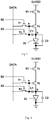
- a pixel circuit comprises: a power supply terminal ELVDD; a control thin film transistor Tc; a drive thin film transistor Td; a storage capacitor C1; a light-emitting device 20; a voltage division control module 10; and a voltage division capacitor C2.
- a first electrode of the control thin film transistor Tc is connected to the power supply terminal ELVDD, and the control thin film transistor Tc is turned on in a pre-charging phase (the phase 1 in Fig.2 ), a compensation phase (the phase 2 in Fig.2 ) and a light-emitting phase (the phase 4 in Fig.2 ) of the pixel circuit.
- a first electrode of the drive thin film transistor Td is connected to a second electrode of the control thin film transistor Tc.
- a point indicates a gate of the drive thin film transistor Td
- b point indicates the second electrode of drive thin film transistor Td.
- a first end of the storage capacitor C1 is connected to the second electrode of the drive thin film transistor Td, a second end of the storage capacitor C1 is connected to the gate of the drive thin film transistor Td, in the compensation phase of the pixel circuit, voltage between the first end and the second end of the storage capacitor C1 equals to a threshold voltage V dth of the drive thin film transistor Td.
- the second electrode of the drive thin film transistor Td is connected to an anode of the light-emitting device 20, and a cathode of the light-emitting device 20 is grounded.
- the voltage division control module 10 is used for charging the storage capacitor C1 in the pre-charging phase (the phase 1 in Fig.2 ) of the pixel circuit, so that voltage of the gate of the drive thin film transistor Td becomes a reference voltage V ref .
- a first end of the voltage division capacitor C2 is connected to the first end of the storage capacitor C1, and a second end of the voltage division capacitor C2 is connected to the cathode of the light-emitting device 20.
- the power supply terminal ELVDD is connected to a power supply for supplying a voltage to enable the light-emitting device 20 to emit light.
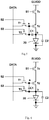
- Timing chart of power signal supplied by the power supply is shown in Fig.2 , in the pre-charging phase (the phase 1 in Fig.2 ), a low level signal ELVDD_L is inputted to the power supply terminal ELVDD, in the compensation phase (the phase 2 in Fig.2 ), the writing phase (the phase 2 in Fig.2 ) and the light-emitting phase (the phase 4 in Fig.2 ), a high level signal ELVDD_H is inputted to the power supply terminal ELVDD.
- the light-emitting device 20 is an organic light-emitting device, it is easy to understand that, when potential of the anode of the light-emitting device 20 is higher than that of the cathode of the light-emitting device 20, the light-emitting device 20 begins to emit light.
- the control thin film transistor Tc is turned on, the voltage division control module 10 charges the storage capacitor C1, so that voltage of the gate of the drive thin film transistor Td becomes the reference voltage V ref .
- the voltage division control module 10 outputs a low level to the second end of the storage capacitor C1, at this time, the drive thin film transistor Td is still turned on, and the control thin film transistor Tc is also turned on, and level of the first end of the storage capacitor C1 is pulled up through the high level ELVDD_H supplied by the power supply terminal ELVDD.
- the second electrode of the drive thin film transistor Td functions as a source of the drive thin film transistor Td.
- the first end and the second end of the storage capacitor C1 are connected between the gate and source of the drive thin film transistor Td respectively, since the potential of the gate is V ref , and the potential of the source has been pulled up by the high level supplied by the power supply terminal, thus the potential of the first end of the storage capacitor C1 is different from the potential of the second end of the storage capacitor C1, the storage capacitor C1 begins to discharge, till the potential Va of the second end of the storage capacitor C1 is smaller than the potential Vb of the first end of the storage capacitor C1, at this time, the drive thin film transistor Td is turned off and the storage capacitor C1 stops discharging and stores the threshold voltage V dth of the drive thin film transistor Td.
- control thin film transistor Tc is turned off, and the storage capacitor C1 is connected between the gate and the second electrode of the drive thin film transistor Td so as to keep the voltage between the gate and the source of the drive thin film transistor Td.
- data voltage is applied to the pixel circuit, so that gate voltage of the drive thin film transistor Td is changed to V data .
- variation ⁇ V 1 of the gate voltage of the drive thin film transistor Td is (V data -V ref ).
- the current flowing through the light-emitting device 20 is independent of the threshold voltage V dth of the drive thin film transistor Td, thus influence of the threshold voltage on the display is substantially eliminated, brightness uniformity of the display panel comprising the pixel circuit is improved, display defects such as mura can be eliminated. Furthermore, even if the threshold voltage of the drive thin film transistor is drifted over time, the current flowing through the light-emitting device will not be affected, therefore, ghost in the display panel comprising the pixel circuit can be eliminated.
- the compensation phase and light-emitting phase of the pixel circuit may further comprise a first control terminal connected to the gate of the control thin film transistor Tc.
- Control signal may be input to the gate of the control thin film transistor Tc through the first control terminal, specifically, in the pre-charging phase, the compensation phase and light-emitting phase, a high level signal is inputted to the gate of the control thin film transistor Tc, and in the data writing phase, a low level signal is inputted to the gate of the control thin film transistor Tc.
- the voltage division control module 10 may charge the storage capacitor in the pre-charging phase of the pixel circuit, so that the gate voltage of the drive thin film transistor reaches the reference voltage, and output a low level to the second end of the storage capacitor in the compensation phase so as to ensure that the storage capacitor may discharge normally in the compensation phase.
- the voltage division control module 10 may comprise a first thin film transistor T1, a second thin film transistor T2, a second control terminal, a third control terminal and a reference voltage terminal, wherein the reference voltage terminal is used to supply the reference voltage, a first electrode of the first thin film transistor T1 is connected to a data input terminal of the pixel circuit, a second electrode of the second thin film transistor T2 is connected to the gate of the drive thin film transistor Td, a gate of the first thin film transistor T1 is connected to the second control terminal, the second control terminal is capable of turning on the first thin film transistor T1 in the data writing phase of the pixel circuit, the first electrode of the second thin film transistor T2 is connected to the reference voltage terminal (in the embodiment shown in Fig.1 , the reference voltage terminal and the data input terminal are formed integrally), the second electrode of the second thin film transistor T2 is connected to the second end of the storage capacitor C1, a gate of the second thin film transistor T2 is connected to the
- the reference voltage V ref is low level. Therefore, in the compensation phase, the reference voltage outputted from the voltage division control module to the storage capacitor C1 is low level, ensuring normal discharge of the storage capacitor C1.
- the first thin film transistor T1 is turned off, at this time, the power supply terminal ELVDD has low level ELVDD_L so as to ensure the light-emitting device 20 not to emit light, the second thin film transistor T2 is turned on, the reference voltage V ref is supplied to the first electrode of the second thin film transistor T2 through the reference voltage terminal, since the second thin film transistor T2 is turned on, gate voltage of fourth thin film transistor T4 also becomes the reference voltage V ref .
- the first thin film transistor T1 is still turned off, the power supply terminal ELVDD has high level ELVDD_H, the control thin film transistor Tc is turned on, the second thin film transistor T2 is turned on, the drive thin film transistor Td is turned on, voltage of the second electrode of the drive thin film transistor Td (that is, the b point in the figure) is pulled up by the ELVDD_H, till the gate-source voltage of the drive thin film transistor Td (Va-Vb) ⁇ V dth , at this time, the drive thin film transistor Td is turned off, and the storage capacitor C1 stores therein the threshold voltage V dth of the drive thin film transistor Td.
- the control thin film transistor Tc and the second thin film transistor T2 are turned off, the first thin film transistor T1 and the drive thin film transistor Td are turned on, thus the storage capacitor C1 is connected between the gate and second electrode (that is, the source) of the drive thin film transistor Td so as to keep the gate-source voltage of the drive thin film transistor, the data voltage is written through the first thin film transistor T1 and the gate voltage of the drive thin film transistor Td is changed to V data .
- the second control terminal and the third control terminal have low level, and the first control terminal has high level, thus the control thin film transistor Tc is turned on, the power supply terminal ELVDD supplies the high level ELVDD_H to enable the light-emitting device 20 to emit light, therefore current flows through the light-emitting device 20 so that the light-emitting device 20 emits light.
- the reference voltage terminal and the data input terminal are formed integrally. That is, the data voltage and the reference voltage may be supplied through the data line, the reference voltage V ref is low level with respect to the data voltage V data .
- a display substrate comprises a plurality of pixel units arranged in rows and columns, each of the pixel units is provided therein with the above pixel circuit. Since when the pixel circuit is emitting light, current flowing through the light-emitting device is independent of the threshold voltage of the drive thin film transistor, the brightness of the light-emitting device is immune to the drift of the threshold voltage of the drive thin film transistor, and immune to the non-uniformity of film thickness of the light-emitting device, that is to say, a display panel comprising the display substrate may have good brightness uniformity and cannot generate display defects such as mura and ghost.
- the display substrate provided in the present invention may be applied to the active matrix organic light-emitting diode display device. That is, the display substrate may include plural groups of scan lines, each group of scan lines corresponds to a row of pixel units.
- each group of scan lines includes a first scan line S1 connected to the first control terminal, for turning on the control thin film transistor Tc in the pre-charging phase, the compensation phase and the light-emitting phase.
- Fig.2 shows the timing chart of scan signal in the first scan line S1.
- the voltage division control module comprises the first thin film transistor T1, the second thin film transistor T2, the second control terminal and the third control terminal, wherein the first electrode of the first thin film transistor T1 is connected to the data input terminal, the second electrode of the second thin film transistor T2 is connected to the gate of the drive thin film transistor Td, the gate of the first thin film transistor T1 is connected to the second control terminal.
- each group of scan lines includes a second scan line S2 and a third scan line S3, the second control terminal is connected to the second scan line S2 for turning on the first thin film transistor T1 in the data writing phase of the pixel circuit, the first electrode of the second thin film transistor T2 is connected to the reference voltage terminal, the second electrode of the second thin film transistor T2 is connected to the second end of the storage capacitor C1, the gate of the second thin film transistor T2 is connected to the third control terminal, the third control terminal is connected to the third scan line S3 for turning on the second thin film transistor T2 in the pre-charging phase and the compensation phase of the pixel circuit.
- Fig.2 shows timing charts of scan signals in the second scan line S2 and the third scan line S3.
- the display substrate further comprises a reference voltage line connected to the first electrode of the second thin film transistor, for supplying the reference voltage to the second thin film transistor in the pre-charging phase.
- the display substrate comprises a data line DATA, which is integrally formed with the reference voltage line (that is, the data line DATA may supply not only data voltage but also reference voltage), the data line is connected to the data input terminal, and the data line may supply reference voltage to the data input terminal in the pre-charging phase, the compensation phase and the light-emitting phase, and supply data voltage to the data input terminal in the data writing phase.
- the data line DATA may supply not only data voltage but also reference voltage
- the data line is connected to the data input terminal
- the data line may supply reference voltage to the data input terminal in the pre-charging phase, the compensation phase and the light-emitting phase, and supply data voltage to the data input terminal in the data writing phase.
- a display panel comprising the above display substrate, wherein the display panel further comprises a power supply connected to the power supply terminal, and the power supply is capable of outputting a low level signal to the power supply terminal in the pre-charging phase of the pixel circuit, and outputting a high level signal to the power supply terminal in the compensation phase, the data writing phase and the light-emitting phase of the pixel circuit.
- the display panel provided in the present invention is especially applicable to large-sized displays such as TV, display of computer and the like.
Landscapes
- Engineering & Computer Science (AREA)
- Physics & Mathematics (AREA)
- Computer Hardware Design (AREA)
- General Physics & Mathematics (AREA)
- Theoretical Computer Science (AREA)
- Electroluminescent Light Sources (AREA)
- Control Of Indicators Other Than Cathode Ray Tubes (AREA)
- Control Of El Displays (AREA)
Applications Claiming Priority (2)
| Application Number | Priority Date | Filing Date | Title |
|---|---|---|---|
| CN201410637704.XA CN104299572B (zh) | 2014-11-06 | 2014-11-06 | 像素电路、显示基板和显示面板 |
| PCT/CN2015/076264 WO2016070570A1 (fr) | 2014-11-06 | 2015-04-10 | Circuit de pixel, substrat d'affichage et panneau d'affichage |
Publications (2)
| Publication Number | Publication Date |
|---|---|
| EP3217385A1 true EP3217385A1 (fr) | 2017-09-13 |
| EP3217385A4 EP3217385A4 (fr) | 2018-05-30 |
Family
ID=52319273
Family Applications (1)
| Application Number | Title | Priority Date | Filing Date |
|---|---|---|---|
| EP15762467.7A Ceased EP3217385A4 (fr) | 2014-11-06 | 2015-04-10 | Circuit de pixel, substrat d'affichage et panneau d'affichage |
Country Status (4)
| Country | Link |
|---|---|
| US (1) | US9875690B2 (fr) |
| EP (1) | EP3217385A4 (fr) |
| CN (1) | CN104299572B (fr) |
| WO (1) | WO2016070570A1 (fr) |
Cited By (2)
| Publication number | Priority date | Publication date | Assignee | Title |
|---|---|---|---|---|
| EP3279889A4 (fr) * | 2015-04-03 | 2018-08-08 | Boe Technology Group Co. Ltd. | Circuit de pixels et son procédé de pilotage, substrat de matrice et dispositif d'affichage |
| CN110322841A (zh) * | 2018-03-27 | 2019-10-11 | 夏普株式会社 | 利用发光器件初始化的tft像素阈值电压补偿电路 |
Families Citing this family (26)
| Publication number | Priority date | Publication date | Assignee | Title |
|---|---|---|---|---|
| CN104299572B (zh) | 2014-11-06 | 2016-10-12 | 京东方科技集团股份有限公司 | 像素电路、显示基板和显示面板 |
| CN104778922B (zh) * | 2015-04-28 | 2017-12-12 | 温州洪启信息科技有限公司 | 一种amoled像素驱动电路及其驱动方法 |
| CN104778925B (zh) * | 2015-05-08 | 2019-01-01 | 京东方科技集团股份有限公司 | Oled像素电路、显示装置及控制方法 |
| CN105185816A (zh) | 2015-10-15 | 2015-12-23 | 京东方科技集团股份有限公司 | 阵列基板及其制造方法、显示装置 |
| US11600234B2 (en) | 2015-10-15 | 2023-03-07 | Ordos Yuansheng Optoelectronics Co., Ltd. | Display substrate and driving method thereof |
| CN105489165B (zh) * | 2016-01-29 | 2018-05-11 | 深圳市华星光电技术有限公司 | 像素补偿电路、方法、扫描驱动电路及平面显示装置 |
| KR102730406B1 (ko) * | 2016-12-12 | 2024-11-18 | 삼성디스플레이 주식회사 | 화소 및 이를 가지는 유기전계발광 표시장치 |
| CN107680530A (zh) * | 2017-09-28 | 2018-02-09 | 深圳市华星光电半导体显示技术有限公司 | 像素补偿电路、扫描驱动电路及显示面板 |
| TWI676978B (zh) * | 2018-10-12 | 2019-11-11 | 友達光電股份有限公司 | 畫素電路 |
| CN109785800B (zh) * | 2019-03-05 | 2020-12-22 | 北京大学深圳研究生院 | 一种微显示像素电路 |
| CN110164361B (zh) * | 2019-06-05 | 2020-12-25 | 京东方科技集团股份有限公司 | 一种像素驱动电路及其驱动方法,以及显示面板 |
| US11402687B2 (en) | 2019-07-18 | 2022-08-02 | Apple Inc. | Display backlighting systems with cancellation architecture for canceling ghosting phenomena |
| US12266303B2 (en) | 2019-08-23 | 2025-04-01 | Boe Technology Group Co., Ltd. | Display device and manufacturing method thereof |
| EP4020447B1 (fr) | 2019-08-23 | 2024-03-27 | BOE Technology Group Co., Ltd. | Circuit de pixels et son procédé d'excitation, substrat d'affichage et son procédé d'excitation, et dispositif d'affichage |
| CN112703604B (zh) | 2019-08-23 | 2024-06-18 | 京东方科技集团股份有限公司 | 显示装置及其制备方法 |
| US11600681B2 (en) | 2019-08-23 | 2023-03-07 | Boe Technology Group Co., Ltd. | Display device and manufacturing method thereof |
| EP4020449B1 (fr) | 2019-08-23 | 2025-06-25 | BOE Technology Group Co., Ltd. | Dispositif d'affichage et son procédé de fabrication |
| US12029065B2 (en) | 2019-08-23 | 2024-07-02 | Boe Technology Group Co., Ltd. | Display device and manufacturing method thereof and driving substrate |
| CN112840461B (zh) | 2019-08-23 | 2025-02-25 | 京东方科技集团股份有限公司 | 显示面板及其制造方法、显示装置 |
| US11404451B2 (en) | 2019-08-27 | 2022-08-02 | Boe Technology Group Co., Ltd. | Electronic device substrate, manufacturing method thereof, and electronic device |
| KR20250167135A (ko) * | 2019-10-11 | 2025-11-28 | 가부시키가이샤 한도오따이 에네루기 켄큐쇼 | 표시 장치 및 전자 기기 |
| CN112164370B (zh) * | 2020-10-28 | 2022-01-11 | 京东方科技集团股份有限公司 | 像素电路及其驱动方法、电子设备 |
| CN113257196A (zh) * | 2021-05-14 | 2021-08-13 | Tcl华星光电技术有限公司 | 背光驱动电路及其控制方法、显示面板、电子装置 |
| US20250008788A1 (en) * | 2022-04-20 | 2025-01-02 | Chengdu Boe Optoelectronics Technology Co., Ltd. | Display panel and display device |
| CN114999400A (zh) * | 2022-06-17 | 2022-09-02 | 长沙惠科光电有限公司 | 像素驱动电路和显示面板 |
| CN116206566B (zh) * | 2023-01-31 | 2026-03-17 | 惠科股份有限公司 | 像素驱动电路及显示装置 |
Family Cites Families (14)
| Publication number | Priority date | Publication date | Assignee | Title |
|---|---|---|---|---|
| JP2003043994A (ja) * | 2001-07-27 | 2003-02-14 | Canon Inc | アクティブマトリックス型ディスプレイ |
| JP2009116206A (ja) * | 2007-11-09 | 2009-05-28 | Sony Corp | El表示パネル及び電子機器 |
| KR100936882B1 (ko) * | 2008-06-11 | 2010-01-14 | 삼성모바일디스플레이주식회사 | 유기전계발광 표시장치 |
| JP4640472B2 (ja) * | 2008-08-19 | 2011-03-02 | ソニー株式会社 | 表示装置、表示駆動方法 |
| KR101269360B1 (ko) * | 2009-05-25 | 2013-05-29 | 파나소닉 주식회사 | 화상 표시 장치 |
| KR101073281B1 (ko) * | 2010-05-10 | 2011-10-12 | 삼성모바일디스플레이주식회사 | 유기전계발광 표시장치 및 그의 구동방법 |
| CN101976545A (zh) * | 2010-10-26 | 2011-02-16 | 华南理工大学 | Oled显示器的像素驱动电路及其驱动方法 |
| CN101980330B (zh) * | 2010-11-04 | 2012-12-05 | 友达光电股份有限公司 | 有机发光二极管的像素驱动电路 |
| CN102708785B (zh) * | 2011-05-18 | 2015-06-24 | 京东方科技集团股份有限公司 | 像素单元电路及其工作方法、oled显示装置 |
| CN103440840B (zh) * | 2013-07-15 | 2015-09-16 | 北京大学深圳研究生院 | 一种显示装置及其像素电路 |
| CN103714781B (zh) | 2013-12-30 | 2016-03-30 | 京东方科技集团股份有限公司 | 栅极驱动电路、方法、阵列基板行驱动电路和显示装置 |
| CN103943067B (zh) | 2014-03-31 | 2017-04-12 | 京东方科技集团股份有限公司 | 一种像素电路及其驱动方法、显示装置 |
| CN204117566U (zh) * | 2014-11-06 | 2015-01-21 | 京东方科技集团股份有限公司 | 像素电路、显示基板和显示面板 |
| CN104299572B (zh) | 2014-11-06 | 2016-10-12 | 京东方科技集团股份有限公司 | 像素电路、显示基板和显示面板 |
-
2014
- 2014-11-06 CN CN201410637704.XA patent/CN104299572B/zh active Active
-
2015
- 2015-04-10 EP EP15762467.7A patent/EP3217385A4/fr not_active Ceased
- 2015-04-10 US US14/777,808 patent/US9875690B2/en active Active
- 2015-04-10 WO PCT/CN2015/076264 patent/WO2016070570A1/fr not_active Ceased
Cited By (4)
| Publication number | Priority date | Publication date | Assignee | Title |
|---|---|---|---|---|
| EP3279889A4 (fr) * | 2015-04-03 | 2018-08-08 | Boe Technology Group Co. Ltd. | Circuit de pixels et son procédé de pilotage, substrat de matrice et dispositif d'affichage |
| EP3955239A1 (fr) * | 2015-04-03 | 2022-02-16 | BOE Technology Group Co., Ltd. | Circuit de pixels, son procédé de fonctionnement et son procédé de commande, substrat de réseau et dispositif d'affichage |
| CN110322841A (zh) * | 2018-03-27 | 2019-10-11 | 夏普株式会社 | 利用发光器件初始化的tft像素阈值电压补偿电路 |
| CN110322841B (zh) * | 2018-03-27 | 2021-12-10 | 夏普株式会社 | 利用发光器件初始化的tft像素阈值电压补偿电路 |
Also Published As
| Publication number | Publication date |
|---|---|
| US9875690B2 (en) | 2018-01-23 |
| CN104299572A (zh) | 2015-01-21 |
| US20160293105A1 (en) | 2016-10-06 |
| EP3217385A4 (fr) | 2018-05-30 |
| WO2016070570A1 (fr) | 2016-05-12 |
| CN104299572B (zh) | 2016-10-12 |
Similar Documents
| Publication | Publication Date | Title |
|---|---|---|
| US9875690B2 (en) | Pixel circuit, display substrate and display panel | |
| US10545592B2 (en) | Touch display module, method for driving the same, touch display panel and touch display device | |
| US9214506B2 (en) | Pixel unit driving circuit, method for driving pixel unit driving circuit and display device | |
| US9812082B2 (en) | Pixel circuit, driving method, display panel and display device | |
| US8941309B2 (en) | Voltage-driven pixel circuit, driving method thereof and display panel | |
| US9734760B2 (en) | Sensing circuit for external compensation, sensing method thereof and display apparatus | |
| KR101382001B1 (ko) | 화소 유닛 회로 및 oled 표시 장치 | |
| EP2523182B1 (fr) | Procédé pour opération de réduction de CO de charge partielle pour une turbine à gaz séquentielle | |
| KR102091485B1 (ko) | 유기 발광 표시 장치 및 그의 구동 방법 | |
| CN103218970B (zh) | Amoled像素单元及其驱动方法、显示装置 | |
| US10032415B2 (en) | Pixel circuit and driving method thereof, display device | |
| US9852685B2 (en) | Pixel circuit and driving method thereof, display apparatus | |
| CN103258501B (zh) | 一种像素电路及其驱动方法 | |
| US9548024B2 (en) | Pixel driving circuit, driving method thereof and display apparatus | |
| US20190180675A1 (en) | Light emitting display apparatus and method for driving thereof | |
| US20080030446A1 (en) | Display apparatus and driving method for display apparatus | |
| US20150339974A1 (en) | Pixel unit circuit, compensating method thereof and display device | |
| US20200082756A1 (en) | Display Panel, Display Device and Compensation Method | |
| US20180357962A1 (en) | Pixel circuit, driving method thereof, display panel and display apparatus | |
| US20210335237A1 (en) | Pixel Driving Circuit and Method, Display Apparatus | |
| US20140118420A1 (en) | Pixel circuit and display apparatus | |
| US20190259335A1 (en) | Pixel driving circuitry and method for driving the same, display substrate and display device | |
| US10223967B1 (en) | OLED pixel driving circuit and pixel driving method | |
| CN104537984B (zh) | 一种像素电路及其驱动方法 | |
| JP5028207B2 (ja) | 画像表示装置および画像表示装置の駆動方法 |
Legal Events
| Date | Code | Title | Description |
|---|---|---|---|
| PUAI | Public reference made under article 153(3) epc to a published international application that has entered the european phase |
Free format text: ORIGINAL CODE: 0009012 |
|
| 17P | Request for examination filed |
Effective date: 20150918 |
|
| AK | Designated contracting states |
Kind code of ref document: A1 Designated state(s): AL AT BE BG CH CY CZ DE DK EE ES FI FR GB GR HR HU IE IS IT LI LT LU LV MC MK MT NL NO PL PT RO RS SE SI SK SM TR |
|
| AX | Request for extension of the european patent |
Extension state: BA ME |
|
| DAV | Request for validation of the european patent (deleted) | ||
| DAX | Request for extension of the european patent (deleted) | ||
| A4 | Supplementary search report drawn up and despatched |
Effective date: 20180503 |
|
| RIC1 | Information provided on ipc code assigned before grant |
Ipc: G09G 3/32 20160101AFI20180425BHEP |
|
| REG | Reference to a national code |
Ref country code: DE Ref legal event code: R003 |
|
| STAA | Information on the status of an ep patent application or granted ep patent |
Free format text: STATUS: THE APPLICATION HAS BEEN REFUSED |
|
| 18R | Application refused |
Effective date: 20191113 |