EP3217558A1 - Messung von timing-differenz - Google Patents
Messung von timing-differenz Download PDFInfo
- Publication number
- EP3217558A1 EP3217558A1 EP16160038.2A EP16160038A EP3217558A1 EP 3217558 A1 EP3217558 A1 EP 3217558A1 EP 16160038 A EP16160038 A EP 16160038A EP 3217558 A1 EP3217558 A1 EP 3217558A1
- Authority
- EP
- European Patent Office
- Prior art keywords
- circuitry
- current
- signal
- signals
- dependence
- Prior art date
- Legal status (The legal status is an assumption and is not a legal conclusion. Google has not performed a legal analysis and makes no representation as to the accuracy of the status listed.)
- Granted
Links
Images




Classifications
-
- H—ELECTRICITY
- H03—ELECTRONIC CIRCUITRY
- H03L—AUTOMATIC CONTROL, STARTING, SYNCHRONISATION OR STABILISATION OF GENERATORS OF ELECTRONIC OSCILLATIONS OR PULSES
- H03L7/00—Automatic control of frequency or phase; Synchronisation
- H03L7/06—Automatic control of frequency or phase; Synchronisation using a reference signal applied to a frequency- or phase-locked loop
- H03L7/08—Details of the phase-locked loop
- H03L7/085—Details of the phase-locked loop concerning mainly the frequency- or phase-detection arrangement including the filtering or amplification of its output signal
-
- H—ELECTRICITY
- H03—ELECTRONIC CIRCUITRY
- H03L—AUTOMATIC CONTROL, STARTING, SYNCHRONISATION OR STABILISATION OF GENERATORS OF ELECTRONIC OSCILLATIONS OR PULSES
- H03L7/00—Automatic control of frequency or phase; Synchronisation
- H03L7/06—Automatic control of frequency or phase; Synchronisation using a reference signal applied to a frequency- or phase-locked loop
- H03L7/08—Details of the phase-locked loop
- H03L7/085—Details of the phase-locked loop concerning mainly the frequency- or phase-detection arrangement including the filtering or amplification of its output signal
- H03L7/091—Details of the phase-locked loop concerning mainly the frequency- or phase-detection arrangement including the filtering or amplification of its output signal the phase or frequency detector using a sampling device
-
- G—PHYSICS
- G04—HOROLOGY
- G04F—TIME-INTERVAL MEASURING
- G04F1/00—Apparatus which can be set and started to measure-off predetermined or adjustably-fixed time intervals without driving mechanisms, e.g. egg timers
- G04F1/005—Apparatus which can be set and started to measure-off predetermined or adjustably-fixed time intervals without driving mechanisms, e.g. egg timers using electronic timing, e.g. counting means
-
- G—PHYSICS
- G04—HOROLOGY
- G04F—TIME-INTERVAL MEASURING
- G04F10/00—Apparatus for measuring unknown time intervals by electric means
- G04F10/005—Time-to-digital converters [TDC]
Definitions
- the present invention relates to circuitry for measuring a timing difference between signals, for example for use in a phase detector/comparator of phase-locked loop or phase-lock loop (PLL) circuitry.
- PLL phase-lock loop
- FIG. 1 is a schematic diagram of example PLL circuitry 1.
- PLL circuitry 1 comprises a reference clock (REFCLK) source 2, a phase comparator 4, a charge pump 6, a loop filter 8, a voltage-controlled oscillator (VCO) 10, a clock-controlled circuit 12, and a divider 14.
- REFCLK reference clock
- VCO voltage-controlled oscillator
- the charge pump 6 is connected to be controlled by the output of the phase comparator 4.
- the VCO 10 outputs one or more clock signals (in the case of Figure 1 , four clock signals) to the clock-controlled circuit 12.
- One or more of the clock signals (VCOCLK) output from the VCO are also fed back via the divider 14 as a clock signal VCODIV to the phase comparator, which also receives an input from the reference clock source 2.
- the PLL circuitry 1 serves to lock the clock signal or clock signals output by the VCO 10 into phase alignment with the reference clock signal REFCLK, with some difference in frequency between the clock signals REFCLK and VCOCLK dependent on the divider ratio set in the divider 14.
- VCO 10 Although typical VCO circuits output a single clock signal, the VCO 10 is indicated as outputting four clock signals as mentioned above. This is to indicate the applicability of the PLL circuitry 1 (and indeed of embodiments of the present invention) to the analogue-to-digital converter (ADC) circuitry of EP2211468 , the entire contents of which are incorporated herein by reference, and to the digital-to-analogue converter (DAC) circuitry of EP2849345 , again the entire contents of which are incorporated herein by reference.
- ADC analogue-to-digital converter
- DAC digital-to-analogue converter
- the ADC circuitry operates based on quadrature (4-phase) clock signals, comprising four time-interleaved substantially sinusoidal clock signals having relative phases 0°, 90°, 180° and 270°.
- quadrature (4-phase) clock signals comprising four time-interleaved substantially sinusoidal clock signals having relative phases 0°, 90°, 180° and 270°.
- the DAC circuitry of EP2849345 for which see for example Figure 15B of that document.
- the clock-controlled circuitry 12 of Figure 1 is indicated as being an ADC or DAC by way of example, and this example will be continued as a running example here with the understanding that the clock-controlled circuitry 12 could be any circuitry operable based on one or more clock signals.
- Figure 2 presents a signal diagram of its input clock signals, namely the clock signal VCODIV being the clock signal fed back from the VCO 10 via the divider 14, and the reference clock signal REFCLK.
- PLL circuitry such as PLL circuitry 1 is to maintain a relationship between the clock signal VCODIV and the reference clock signal REFCLK, so that there is also a (demanded or target) relationship between the clock signal VCOCLK fed to the clock-controlled circuit 12 and the reference clock signal REFCLK.
- phase comparator 4 phase detector
- the job of the phase comparator 4 may be summarised as to create an output signal to be fed along the path to the VCO 10 such that a desired X cycles of the clock signal VCODIV occur for each 1 cycle of the reference clock signal REFCLK, as indicated in Figure 2 .
- clock signal VCODIV is shown in Figure 2
- the clock signal VCO itself or a clock signal derived therefrom could equally be shown, with the value X adjusted accordingly. For this reason, such signals will be generically indicated as being VCO hereinafter.
- the challenge is to maintain such an integer and fraction relationship as accurately as possible for the PLL circuitry 1 to output the intended VCO clock frequency (i.e. achieve the target locked state). This will of course affect the operation of the clock-controlled circuitry 12.
- current-mode circuitry for measuring a timing difference between first and second signals, the circuitry comprising: a tail node configured during a measurement operation to receive a current pulse in dependence upon the first signal; first and second nodes conductively connectable to said tail node along respective first and second paths; and steering circuitry configured during the measurement operation to control such connections between the tail node and the first and second nodes based on the second signal to steer the current pulse so that a first portion of the current pulse passes along the first path and a second portion of the current pulse passes along the second path in dependence upon the timing difference between said first and second signals.
- references to current-mode circuitry could be expressed as references to charge-mode circuitry.
- charge is the integral of current over a pulse period.
- the current pulse may be described simply as a current in some embodiments.
- Such circuitry may comprise a signal output unit configured to output a measurement-result signal indicating a measure of said timing difference based upon one or both of the first and second portions.
- the technique of dividing a current pulse based upon the timing difference between the first and second signals advantageously enables accurate measurements to be taken. For example, current-splitting can be done accurately even with high-frequency signals.
- the steering circuitry is configured to steer the current such that the first portion passes along the first path and then the second portion passes along the second path. That is, the current passes firstly along one of the paths and then along the other, with perhaps only a transitional period over which some current passes along both paths simultaneously (relating to rise/fall times etc.).
- the control circuitry may comprise switching circuitry provided along the paths, the switching circuitry configured such that the conductivity of the connections between the tail node and the first and second nodes is controlled by the second signal.
- Such switching circuitry may comprise transistors such as MOSFETs.
- the switching circuitry may comprise a first transistor whose channel forms part of the first path and a second transistor whose channel forms part of the second path, wherein gate terminals of those transistors are controlled by the second signal.
- the circuitry may comprise a controllable (e.g. voltage controlled) current source configured to provide said current pulse in dependence upon the first signal.
- the first signal is preferably a square-wave, or switched logic-level signal, such that the current pulse has a switched logic-level form, i.e. a flat (linear) top at least over a central portion of the pulse. This may enable linear operation of the circuitry, improving the accuracy in the measures.
- the signal output unit may be configured to output the measurement-result signal based upon a difference in the size of the first and second portions, or in dependence upon the size of one of the first and second portions.
- the signal output unit may comprise first and second capacitances connected to the first and second nodes, respectively, for converting the first and second portions of the current pulse into corresponding first and second potential differences. Such potential differences or voltages may be readily employed by further circuitry.
- the signal output unit may comprise analogue-to-digital conversion circuitry and the measurement-result signal may be a digital signal.
- circuitry according to the present aspect may be referred to as time-to-digital converter (TDC) circuitry.
- first and second signals may be switched logic level signals.
- at least the first signal is a switched logic level signal since it controls the form of the current pulse.
- a current pulse with a switched-level or switched logic-level form may facilitate linear operation of circuitry according to the present aspect.
- Such switched level signals have rising and falling edges, which may be readily detected for example.
- the first and second signals may be clock signals, or other repetitive signals e.g. with a repeating pattern of edges.
- phase detector comprising current-mode circuitry according to the aforementioned first aspect of the present invention.
- the current-mode circuitry may be configured to repeatedly measure such timing differences between the first and second signals, generating a sequence of measures of the timing differences.
- Such a phase detector may comprise: reference circuitry operable, in dependence upon a target (or demanded or input or reference) relationship between said first and second signals, to generate a sequence of reference values indicating timing differences between the first and second signals corresponding to (or meeting or respecting or satisfying) the target relationship; comparison circuitry configured to compare the sequence of measures with the sequence of reference values; and a signal output unit operable to output a phase-detection signal in dependence upon a result of the comparison.
- Such a phase detector may also comprise calibration circuitry operable to calibrate operation of the phase detector in dependence upon the sequences of reference values and measures. For example, such circuitry may operate based on error values, corresponding to differences between respective reference values and measures.
- the calibration circuitry may be configured to detect gain and/or offset errors.
- the calibration circuitry may be configured - in order to effect the calibration - to adjust an ADC reference value or tail current of the current-mode circuitry or adjust an offset trim in a comparator in ADC circuitry of the current-mode circuitry, or adjust the timing of clock signals employed, or add an offset to the output measures.
- phase-locked loop circuitry comprising a phase detector according to the aforementioned second aspect of the present invention.
- digital-to-analogue converter circuitry or analogue-to-digital converter circuitry comprising current-mode circuitry according to the aforementioned first aspect of the present invention, or a phase detector according to the aforementioned second aspect of the present invention, or phase-locked loop circuitry according to the aforementioned third aspect of the present invention.
- an IC chip such as a flip chip, comprising current-mode circuitry according to the aforementioned first aspect of the present invention, or a phase detector according to the aforementioned second aspect of the present invention, or phase-locked loop circuitry according to the aforementioned third aspect of the present invention, or digital-to-analogue converter circuitry or analogue-to-digital converter circuitry according to the aforementioned fourth aspect of the present invention.
- the present invention extends to method aspects corresponding to the apparatus aspects.
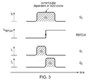
- FIG. 3 is a schematic diagram useful for understanding the general principle behind the present invention.
- the general idea is to create a current pulse in dependence upon the first signal and then to use the second signal to steer that current pulse so that a first portion of it passes along a first path and a second portion of it passes along a second path. Those portions can then be used to output a measurement signal indicating a measure of the timing difference.
- a "total" current I T is shown flowing such that it creates a current pulse (i.e. a pulse or packet of charge) Q T in dependence upon the VCO clock signals, e.g. as output by VCO 12.
- Clock signal REFCLK is also shown with one of its edges, in this example a rising edge, occurring while that current pulse is flowing, with the understanding that clock signal REFCLK is used to direct a (first) portion Q 1 of the pulse Q T along the first path and another (second) portion Q 2 along the second path. In this example, the two portions Q 1 and Q 2 together make up the total pulse Q T .
- the relative sizes of the portions Q 1 and Q 2 will depend on where the rising edge of the clock REFCLK falls compared to the current pulse Q T and thus on the timing difference (i.e. relative timing, or phase difference) between the clock signal REFCLK and the VCO clock signals.
- Figures 4 and 5 are schematic diagrams presenting an embodiment of the present invention.
- Figures 4(a) and 4(b) present circuitry arrangements 20 and 30 respectively. As will become apparent, circuitry arrangements 20 and 30 may be employed in combination, however circuitry arrangement 30 may be employed without circuitry arrangement 20 in some embodiments of the present invention.
- Figures 5(a) to 5(c) are signal timing diagrams useful for understanding the operation of the circuitry arrangements 20 and 30.
- Circuitry arrangement 20 of Figure 4(a) comprises a signal selector 22 and clock distribution circuitry 24.
- Signal selector 22 is operable to select one of a plurality of input signals based on a selection signal SEL and output that selected signal.
- the VCO output clock signals may be quadrature clock signals, namely a set of four timed-interleaved substantially sinusoidal clock signals ⁇ 0 , ⁇ 1 , ⁇ 2 and ⁇ 3 as shown, corresponding to those discussed above in connection with EP2849345 and EP2211468 .
- any one of these clock signals ⁇ 0 to ⁇ 3 could be referred to as the clock signal VCO.
- Figure 5(b) presents equivalent quadrature square-wave switched logic level clock signals, also labelled ⁇ 0 , ⁇ 1 , ⁇ 2 and ⁇ 3 , to indicate that the VCO 10 may output clock signals of different types, depending on the application and clock frequencies employed. Also, the clock signals output from the divider 14 may be such square-wave signals even if its input signal(s) is a sinusoidal signal.
- Embodiments of the present invention may operate on sinusoidal or square-wave clock signals (as well as other shaped of clock signal), however the following description will refer to such square-wave clock signals (e.g. as output by divider 14) for ease of understanding of the present invention.
- square-wave clock signals e.g. as output by divider 14
- the techniques and circuitry disclosed herein may operate based on sinusoidal or square-wave clock signals, it will become apparent that there are significant advantages associated which such square-wave signals (for example, linearity in the operation).
- the signal selector 22 of Figure 5(c) may be supplied with the clock signals ⁇ 0 to ⁇ 3 and may be employed to select the desired one of them based on the selection signal SEL and to output that selection signal as the clock signal ⁇ SEL .
- the circuitry 30 comprises a common tail node 32 and first and second nodes 34 and 36.
- a first signal path 38 connects the common tail node 32 to the first node 34 and a second signal path 40 connects the common tail node 32 to the second node 36.
- a controllable current source 42 is connected to the common tail node 32 and connected to receive the selected clock signal ⁇ SEL as its control signal. As such, the controllable current source 42 is configured to cause the current pulse Q T formed from the current I T (see Figure 3 ) to flow through the common tail node 32 in dependence upon the selected clock signal ⁇ SEL .
- the controllable current source 42 may be considered to cause current I T to flow when the clock signal ⁇ 3 is high, creating the current pulse Q T such that it mirrors in shape the cross-hatched part of the clock signal ⁇ 3 in Figure 5(b) .
- Switches 44 and 46 are provided along the first and second paths 38 and 40, respectively. Those switches 44 and 46 are also connected to be controlled based on clock signals /REFCLK and REFCLK, respectively, provided from clock distribution circuitry 24 in Figure 4(a) .
- Switch 44 is configured to be closed (conductive) when REFCLK is low and open when REFCLK is high, and, conversely, switch 46 is configured to be open when REFCLK is low and closed (conductive) when REFCLK is high.
- switches 44 and 46 could be implemented as NMOS MOSFETs whose channels are connected along paths 38 and 40 respectively and whose gate terminals are controlled by clock signals /REFCLK and REFCLK, respectively.
- the portion Q 1 of the current pulse Q T before the rising edge of the clock REFCLK is caused to flow along the first path 38 and the portion Q 2 of the current pulse Q T after the rising edge of the clock signal REFCLK is caused to flow along the second path 40, in line with Figure 3 .
- the circuitry 30, and specifically the arrangement of switches 44 and 46 along the first and second paths 38 and 40 connected to the common tail node 32 is configured to steer the current pulse Q T from one path to the next over time, dependent on the clock signal REFCLK.
- This current-mode operation affords a high degree of accuracy, because all of the current pulse Q T must flow down one or other of the first and second paths 38 and 40.
- Circuitry 30 further comprises an output signal unit 50, comprising a capacitor bank 52 and an ADC unit 54.
- Capacitor bank 52 comprises capacitors 62 and 64 and reset switches 66 and 68. Capacitors 62 and 64 are connected to the ends of paths 38 and 40 at the first and second nodes 34 and 36, respectively. Thus, pulse portions Q 1 and Q 2 create corresponding potential differences V 1 and V 2 across capacitors 62 and 64. If capacitors 62 and 64 have equal capacitances, then the potential differences V 1 and V 2 are proportional to the amounts of charge in pulse portions Q 1 and Q 2 and consequently are reflective of the position of the rising edge of the clock signal REFCLK relative to the current pulse Q T and thus the timing difference (or phase difference or phase lag) between the clock signals REFCLK and ⁇ SEL .
- V 1 and V 2 for example by looking at the difference V 2 - V 1 or vice versa, it is possible to assess the location of the rising edge of the clock signal REFCLK relative to a rising edge of the clock signal ⁇ SEL .
- this can contribute to an assessment of the fractional part of the value X (the integer part could be assessed e.g. by simple edge counting). Further, to get a single value of X it will be possible to find the relative location of two consecutive rising edges of REFCLK. However, a more practical scheme is to continually "watch" the rising edges of the clock signal REFCLK so as to get a sequence of measures of the relative location of those edges compared to the clock signal ⁇ SEL , i.e. measures of the timing differences between those signals. Such a scheme will be described in more detail below.
- the reset switches 66 and 68 of the circuitry 30 may be used to reset the potential differences across the capacitors 62 and 64 between taking such measures of the timing differences between the signals REFCLK and ⁇ SEL . It will be understood that by looking at the results of multiple conversions, calibration can be used to correct for differences between phases or cycles.
- ADC unit 54 is connected to receive the potential differences V 1 and V 2 or a potential difference generated from them such as V 2 - V 1 , and to output a digital value indicative of the supplied potential difference or differences.
- the output digital value (in the same way as the voltages V 1 and/or V 2 , or indeed V 2 - V 1 ) is a measurement of the timing difference between the clock signals REFCLK and ⁇ SEL .
- circuitry 30 could be referred to as a time-to-digital converter (TDC).
- Figure 6 is a signal timing diagram showing clock signal REFCLK relative to clock signal ⁇ SEL , and thus is similar to parts of Figure 5 .
- an advantage of selecting the one of the clock signals ⁇ 0 to ⁇ 3 which puts the rising edge of the clock signal REFCLK towards the middle of the high period, in the case of Figure 5(b) the cross-hatched portion of clock signal ⁇ 3 , is that the ADC unit 54 (and indeed the voltage signals V 1 and V 2 , and the difference of V 2 - V 1 ) are in a linear region as indicated in Figure 6 .
- the current pulse Q T will not be exactly rectangular shaped, i.e. with perfect rising and falling edges, and thus the middle portion (i.e. minus the leading and trailing edge portions) will be the more linear portion of the pulse.
- the middle portion i.e. minus the leading and trailing edge portions
- the middle portion i.e. minus the leading and trailing edge portions
- the sinusoidal signals of Figure 5(a) since the resulting current pulse will have a flat-topped, square-wave or rectangular shape, aiding the linear relationship between: (a) where REFCLK appears relative to ⁇ SEL ; and (b) the change in voltage signals V 1 and V 2 .
- circuitry 30 could be employed in the phase comparator 4, it may be known which of clocks ⁇ 0 to ⁇ 3 would be in its linear period for each rising edge of the clock signal REFCLK when the PLL circuitry is in or close to being in lock (see Figure 2 ), so that the circuity 20 could be employed to select the appropriate one of the clock signals ⁇ 0 to ⁇ 3 for each rising edge of the clock signal REFCLK, thus negating the need to provide four sets of circuitry 30.
- the integer part of the value X will be known (in the sense that it may be stable or could be calculated rather than needing measurement), and only the fractional part need be measured each time the rising edge of the clock signal REFCLK comes along.
- the value measured by circuitry 30 is Q 1 - Q 2 , effectively V 1 - V 2 . If the REFCLK edge is exactly in the middle of the charge pulse the result is zero (and this can be set as ADC midscale).
- the ADC in circuitry 30 has to cover 90 degrees, this equating to a fine TDC. This 90 degrees is about half the total width of one charge pulse (i.e. each charge pulse is approximately half a cycle wide, equating to 180 degrees).
- a charge pulse split of 25%:75% could be set as ADC negative full scale (e.g. -128 code for an 8b ADC), and a split of 75%:25% (REFCLK late) could be set as ADC positive full scale (e.g. +127 code for an 8b ADC).
- the ADC gain could be lower than this (e.g. by adjusting its reference voltage which sets the charge:code gain) so that 90 degrees does not occupy the entire ADC range (256 LSB).
- the gain could be so that 227 LSB corresponds to 90 degrees, with the output ADC code then being multiplied by 9/8 to get back to a digital range of 256 for calculations.
- FIG 7 is a schematic diagram of PLL circuitry 70 embodying the present invention.
- the PLL circuitry 70 naturally has some similarities with the PLL circuitry 1 of Figure 1 , and thus like elements are denoted in the same way and duplicate description is omitted.
- phase comparator 71 comprises a time-to-digital converter (TDC) 72, a counter 74 and a subtractor 76.
- TDC 72 itself embodies the present invention.
- the phase comparator 71 is connected to receive the reference clock signal REFCLK and the clock signal fed back from the VCO, in this case via the divider 14.
- the TDC 72 within the phase comparator 71, also receives these signals.
- the TDC 72 is operable, based on its received signals, to outputs an integer + fraction value, having measured where the REFCLK rising edge lies and produced a digital output, using the techniques described above in connection with Figures 3 to 6 .
- the TDC 72 may be considered to comprise the circuitry 30, or the circuitry 20 and 30 in combination, of Figure 4 .
- such circuitry is operable to determine how many cycles (integer + fraction) of the VCO clock signal (via monitoring VCODIV - e.g. using a counter) correspond to one cycle of the reference clock signal (REFCLK).
- the TDC 72 is operable to repeatedly output such integer + fraction values, i.e. to repeatedly measure a timing difference between its input signals. That is, it may repeatedly measure the relationship between rising edges of the reference clock signal REFCLK and the VCO clock signal.
- the counter 74 is connected to receive a "demand" or target value, indicating the desired output frequency expressed as how many cycles (integer + fraction) of the VCO clock signal should correspond to one cycle of the reference clock signal (REFCLK).
- the demand value is 73.2169.
- the counter 74 may be configured to receive this demand value as an analogue signal, however preferably it is received as a digital value.
- the counter 74 is also connected to be clocked by the signal REFCLK, and is configured to increment its output by the demand value each time it is clocked.
- its output A (see Figure 7 ) in this example reads 73.2169, 146.4338, 219.6507 etc. as target values associated with successive REFCLK clock cycles (e.g. rising edges).
- the TDC 72 is configured to output an output B of corresponding actual measured values as mentioned above, in this example corresponding to the same successive REFCLK clock cycles as for the values of output A.
- the subtractor 76 is connected to receive outputs A and B as indicated, and to generate difference output C, as also indicated in Figure 7 .
- Example values for outputs A, B and C are indicated together in Figure 7 , and these may all be handled as digital values.
- the output C is the output of the phase comparator 71, and is fed via the loop filter 8 (to average noise) to control the VCO 10, in a similar manner to that already described in connection with Figure 1 .
- Figure 8 presents graphs indicating how the circuitry embodying the present invention may be calibrated or controlled to improve its performance.
- the X-axis is for the predicted fractional values, here shown in relation to a 90° phase range covered by a particular one of the VCO clock phases ⁇ 0 to ⁇ 3 as in Figure 5 (b) , for example phase ⁇ 0 . It will be appreciated that the X-axis may continue to cover the other three phases in a similar way (although not explicitly shown in Figure 8 ).
- the Y-axis is for the measured fractional values, here shown as ADC output codes (i.e. digital values) within the ADC range 0 to 255 as an example. Both such axes could of course be presented in terms of ADC output codes or phase ranges.
- the lower graph in Figure 8 corresponds to the same phase range as for the upper graph, and similarly may extend to cover the other three phases in a similar way (although not shown for simplicity).
- This lower graph is provided to plot the error values corresponding to the plotted values in the graph, for example equating to measured fraction - predicted fraction.
- the form or pattern (e.g. slope and offset) of the trace in the lower graph could be assessed in practice e.g. by accumulating/storing errors associated with the left-hand half of the upper graph (i.e. of a 90° phase range) in one register and those associated with the right-hand half of the upper graph in another register over time. The totals or averages of these values over time may then be indicative of the form or pattern, avoiding the need to actually plot and analyse the graphs per se.
- the above-described circuitry may be provided with control circuitry operable, based on such an analysis or comparison of the predicted and measured values, to control the TDC 72, or other parts of the circuitry 71 or 70, to reduce the errors experienced.
- Gain errors could be compensated for e.g. by trimming the ADC reference value or tail current (i.e. the magnitude of I T ).
- Offset errors could be compensated for by an offset trim in the ADC comparator, adjusting the timing in the clocks, or even adding a digital offset in the TDC output.
- circuitry disclosed herein could be described as circuitry for measuring a timing difference between first and second signals, as a time-to-digital converter, as a phase detector or phase comparator, or as PLL circuitry.
- Such circuitry may be provided as a clock source, for example to control mixed-signal circuitry such as DAC or ADC circuitry.
- Circuitry of the present invention may be implemented as DAC or ADC circuitry.
- Circuitry of the present invention may be implemented as integrated circuitry, for example on an IC chip such as a flip chip.
- the present invention extends to integrated circuitry and IC chips as mentioned above, circuit boards comprising such IC chips, and communication networks (for example, internet fiber-optic networks and wireless networks) and network equipment of such networks, comprising such circuit boards.
Landscapes
- Stabilization Of Oscillater, Synchronisation, Frequency Synthesizers (AREA)
- Manipulation Of Pulses (AREA)
Priority Applications (4)
| Application Number | Priority Date | Filing Date | Title |
|---|---|---|---|
| EP16160038.2A EP3217558B1 (de) | 2016-03-11 | 2016-03-11 | Zeitunterschied messung |
| JP2017045935A JP6880845B2 (ja) | 2016-03-11 | 2017-03-10 | タイミング差異の測定 |
| US15/455,901 US10075172B2 (en) | 2016-03-11 | 2017-03-10 | Timing-difference measurement |
| CN201710141736.4A CN107181486B (zh) | 2016-03-11 | 2017-03-10 | 定时差测量 |
Applications Claiming Priority (1)
| Application Number | Priority Date | Filing Date | Title |
|---|---|---|---|
| EP16160038.2A EP3217558B1 (de) | 2016-03-11 | 2016-03-11 | Zeitunterschied messung |
Publications (2)
| Publication Number | Publication Date |
|---|---|
| EP3217558A1 true EP3217558A1 (de) | 2017-09-13 |
| EP3217558B1 EP3217558B1 (de) | 2020-05-13 |
Family
ID=55527444
Family Applications (1)
| Application Number | Title | Priority Date | Filing Date |
|---|---|---|---|
| EP16160038.2A Active EP3217558B1 (de) | 2016-03-11 | 2016-03-11 | Zeitunterschied messung |
Country Status (4)
| Country | Link |
|---|---|
| US (1) | US10075172B2 (de) |
| EP (1) | EP3217558B1 (de) |
| JP (1) | JP6880845B2 (de) |
| CN (1) | CN107181486B (de) |
Families Citing this family (9)
| Publication number | Priority date | Publication date | Assignee | Title |
|---|---|---|---|---|
| US10069503B2 (en) * | 2016-05-30 | 2018-09-04 | Microsemi Semiconductor Ulc | Method of speeding up output alignment in a digital phase locked loop |
| EP3477864B1 (de) * | 2017-10-31 | 2020-07-08 | Nxp B.V. | Vorrichtung mit einer phasenregelschleife |
| CN111771332B (zh) * | 2018-03-02 | 2023-11-21 | 索尼半导体解决方案公司 | 锁相环电路 |
| US11314107B2 (en) | 2018-09-27 | 2022-04-26 | Macom Technology Solutions Holdings, Inc. | Optical modulation skew adjustment systems and methods |
| US10784845B2 (en) * | 2018-09-27 | 2020-09-22 | Macom Technology Solutions Holdings, Inc. | Error detection and compensation for a multiplexing transmitter |
| US11777702B2 (en) | 2018-09-27 | 2023-10-03 | Macom Technology Solutions Holdings, Inc. | Closed loop lane synchronization for optical modulation |
| CN113054998B (zh) * | 2019-12-26 | 2023-04-18 | 澜至电子科技(成都)有限公司 | 时间数字转换器的线性校准系统、方法及数字锁相环 |
| TWI733415B (zh) * | 2020-04-16 | 2021-07-11 | 瑞昱半導體股份有限公司 | 鎖相迴路裝置與時脈產生方法 |
| US10979059B1 (en) * | 2020-10-26 | 2021-04-13 | Ciena Corporation | Successive approximation register analog to digital converter based phase-locked loop with programmable range |
Citations (6)
| Publication number | Priority date | Publication date | Assignee | Title |
|---|---|---|---|---|
| GB2067371A (en) * | 1980-01-09 | 1981-07-22 | Tektronix Inc | Phase lock system |
| EP0161758A2 (de) * | 1984-05-18 | 1985-11-21 | Tektronix Inc. | 50 % Amplitudenpunkt- und Phasendetektor |
| US6480035B1 (en) * | 1994-02-15 | 2002-11-12 | Rambus, Inc. | Phase detector with minimized phase detection error |
| US20030035499A1 (en) * | 2001-08-15 | 2003-02-20 | Staszewski Robert B. | Direct radio frequency (RF) sampling with recursive filtering method |
| EP2211468A1 (de) | 2009-01-26 | 2010-07-28 | Fujitsu Semiconductor Limited | Abtastung |
| EP2849345A1 (de) | 2013-09-12 | 2015-03-18 | Fujitsu Semiconductor Limited | Schaltungen und Verfahren zur Verwendung in Schaltungen mit gemischten Signalen |
Family Cites Families (18)
| Publication number | Priority date | Publication date | Assignee | Title |
|---|---|---|---|---|
| JPS5831615A (ja) * | 1981-08-18 | 1983-02-24 | Pioneer Electronic Corp | 位相比較回路 |
| US6188268B1 (en) * | 1998-10-30 | 2001-02-13 | Sony Corporation Of Japan | Low side current sink circuit having improved output impedance to reduce effects of leakage current |
| JPS6376508A (ja) * | 1986-09-19 | 1988-04-06 | Toko Inc | 位相比較器 |
| US6236275B1 (en) * | 1997-10-24 | 2001-05-22 | Ericsson Inc. | Digital frequency synthesis by sequential fraction approximations |
| JP3094976B2 (ja) * | 1997-11-19 | 2000-10-03 | 日本電気株式会社 | 同期回路 |
| DE19859515C1 (de) * | 1998-12-22 | 2000-04-20 | Siemens Ag | Digitaler Phasen-Frequenz-Detektor |
| US6587529B1 (en) * | 1999-02-25 | 2003-07-01 | Texas Instruments Incorporated | Phase detector architecture for phase error estimating and zero phase restarting |
| US6124745A (en) * | 1999-05-19 | 2000-09-26 | Analog Devices, Inc. | Delay and interpolation timing structures and methods |
| TW483255B (en) * | 1999-11-26 | 2002-04-11 | Fujitsu Ltd | Phase-combining circuit and timing signal generator circuit for carrying out a high-speed signal transmission |
| US20020097682A1 (en) * | 2000-06-02 | 2002-07-25 | Enam Syed K. | Low frequency loop-back in a high speed optical transceiver |
| US7092474B2 (en) * | 2001-09-18 | 2006-08-15 | Broadcom Corporation | Linear phase detector for high-speed clock and data recovery |
| JP4625849B2 (ja) * | 2008-02-25 | 2011-02-02 | 株式会社東芝 | 発振器制御装置 |
| JP2013081084A (ja) * | 2011-10-04 | 2013-05-02 | Renesas Electronics Corp | デジタルpll回路、半導体集積回路装置 |
| EP2602936B1 (de) * | 2011-12-07 | 2014-02-12 | Telefonaktiebolaget L M Ericsson (Publ) | Analoger Phasenregelkreis mit verbessertem Einrasten |
| CN102843130B (zh) * | 2012-09-18 | 2014-10-08 | 北京大学 | 基于cml逻辑的相位检测器 |
| US8957712B2 (en) * | 2013-03-15 | 2015-02-17 | Qualcomm Incorporated | Mixed signal TDC with embedded T2V ADC |
| CN103152035B (zh) * | 2013-03-27 | 2016-04-13 | 武汉大学 | 一种用于锁相环的可编程延时多路控制信号鉴频鉴相器 |
| EP2849021B1 (de) * | 2013-09-12 | 2020-01-01 | Socionext Inc. | Signalausrichtungsschaltungen und Verfahren |
-
2016
- 2016-03-11 EP EP16160038.2A patent/EP3217558B1/de active Active
-
2017
- 2017-03-10 CN CN201710141736.4A patent/CN107181486B/zh active Active
- 2017-03-10 US US15/455,901 patent/US10075172B2/en active Active
- 2017-03-10 JP JP2017045935A patent/JP6880845B2/ja active Active
Patent Citations (6)
| Publication number | Priority date | Publication date | Assignee | Title |
|---|---|---|---|---|
| GB2067371A (en) * | 1980-01-09 | 1981-07-22 | Tektronix Inc | Phase lock system |
| EP0161758A2 (de) * | 1984-05-18 | 1985-11-21 | Tektronix Inc. | 50 % Amplitudenpunkt- und Phasendetektor |
| US6480035B1 (en) * | 1994-02-15 | 2002-11-12 | Rambus, Inc. | Phase detector with minimized phase detection error |
| US20030035499A1 (en) * | 2001-08-15 | 2003-02-20 | Staszewski Robert B. | Direct radio frequency (RF) sampling with recursive filtering method |
| EP2211468A1 (de) | 2009-01-26 | 2010-07-28 | Fujitsu Semiconductor Limited | Abtastung |
| EP2849345A1 (de) | 2013-09-12 | 2015-03-18 | Fujitsu Semiconductor Limited | Schaltungen und Verfahren zur Verwendung in Schaltungen mit gemischten Signalen |
Also Published As
| Publication number | Publication date |
|---|---|
| US20170264304A1 (en) | 2017-09-14 |
| JP2017163546A (ja) | 2017-09-14 |
| CN107181486B (zh) | 2022-04-22 |
| CN107181486A (zh) | 2017-09-19 |
| JP6880845B2 (ja) | 2021-06-02 |
| EP3217558B1 (de) | 2020-05-13 |
| US10075172B2 (en) | 2018-09-11 |
Similar Documents
| Publication | Publication Date | Title |
|---|---|---|
| US10075172B2 (en) | Timing-difference measurement | |
| US12609709B2 (en) | High linearity phase interpolator | |
| US9531394B1 (en) | Calibration of digital-to-time converter | |
| US9362936B1 (en) | Digital-to-time converter | |
| US8228219B2 (en) | Time-to-digital converter with calibration | |
| US10444338B2 (en) | Transmitter-receiver system | |
| US7816959B1 (en) | Clock circuit for reducing long term jitter | |
| US20090184741A1 (en) | Delay lock loop circuit, phase lock loop circuit, timing generator, semiconductor tester and semiconductor integrated circuit | |
| US9698807B1 (en) | Time signal conversion using dual time-based digital-to-analog converters | |
| US8664994B1 (en) | System to generate a predetermined fractional period time delay | |
| US11942956B2 (en) | Time-to-digital converter and digital phase-locked loop circuit comprising the same | |
| WO2017184966A1 (en) | System and method for electronics timing delay calibration | |
| US7391353B2 (en) | Analog/digital converter | |
| US10753966B2 (en) | Duty cycle estimation | |
| CN105375918A (zh) | 用于检测向rf信号施加的相移的电路 | |
| Raisanen-Ruotsalainen et al. | A time digitizer with interpolation based on time-to-voltage conversion | |
| US20110248757A1 (en) | Digital calibration device and method for high speed digital systems | |
| Das et al. | An accurate fractional period delay generation system | |
| Wu et al. | Resilient cell-based architecture for time-to-digital converter | |
| US8502588B2 (en) | Clock generation system | |
| Nagaraj et al. | A self-calibrating sub-picosecond resolution digital-to-time converter | |
| KR102857548B1 (ko) | 듀티 및 위상 캘리브레이션 장치 및 방법 | |
| Zhang et al. | A 3 mW 1.2–3.6 GHz multi-phase PLL-based clock generator with TDC assisted auto-calibration of loop bandwidth | |
| Raisanen-Ruotsalainen et al. | A BiCMOS time-to-digital converter with 30 ps resolution | |
| Raisanen-Rnotsalainen et al. | Time interval digitization with an integrated 32-phase oscillator |
Legal Events
| Date | Code | Title | Description |
|---|---|---|---|
| PUAI | Public reference made under article 153(3) epc to a published international application that has entered the european phase |
Free format text: ORIGINAL CODE: 0009012 |
|
| STAA | Information on the status of an ep patent application or granted ep patent |
Free format text: STATUS: THE APPLICATION HAS BEEN PUBLISHED |
|
| AK | Designated contracting states |
Kind code of ref document: A1 Designated state(s): AL AT BE BG CH CY CZ DE DK EE ES FI FR GB GR HR HU IE IS IT LI LT LU LV MC MK MT NL NO PL PT RO RS SE SI SK SM TR |
|
| AX | Request for extension of the european patent |
Extension state: BA ME |
|
| STAA | Information on the status of an ep patent application or granted ep patent |
Free format text: STATUS: REQUEST FOR EXAMINATION WAS MADE |
|
| 17P | Request for examination filed |
Effective date: 20180209 |
|
| RBV | Designated contracting states (corrected) |
Designated state(s): AL AT BE BG CH CY CZ DE DK EE ES FI FR GB GR HR HU IE IS IT LI LT LU LV MC MK MT NL NO PL PT RO RS SE SI SK SM TR |
|
| STAA | Information on the status of an ep patent application or granted ep patent |
Free format text: STATUS: EXAMINATION IS IN PROGRESS |
|
| 17Q | First examination report despatched |
Effective date: 20180723 |
|
| GRAP | Despatch of communication of intention to grant a patent |
Free format text: ORIGINAL CODE: EPIDOSNIGR1 |
|
| STAA | Information on the status of an ep patent application or granted ep patent |
Free format text: STATUS: GRANT OF PATENT IS INTENDED |
|
| INTG | Intention to grant announced |
Effective date: 20191204 |
|
| GRAS | Grant fee paid |
Free format text: ORIGINAL CODE: EPIDOSNIGR3 |
|
| GRAA | (expected) grant |
Free format text: ORIGINAL CODE: 0009210 |
|
| STAA | Information on the status of an ep patent application or granted ep patent |
Free format text: STATUS: THE PATENT HAS BEEN GRANTED |
|
| AK | Designated contracting states |
Kind code of ref document: B1 Designated state(s): AL AT BE BG CH CY CZ DE DK EE ES FI FR GB GR HR HU IE IS IT LI LT LU LV MC MK MT NL NO PL PT RO RS SE SI SK SM TR |
|
| REG | Reference to a national code |
Ref country code: GB Ref legal event code: FG4D |
|
| REG | Reference to a national code |
Ref country code: CH Ref legal event code: EP |
|
| REG | Reference to a national code |
Ref country code: DE Ref legal event code: R096 Ref document number: 602016036245 Country of ref document: DE |
|
| REG | Reference to a national code |
Ref country code: AT Ref legal event code: REF Ref document number: 1271589 Country of ref document: AT Kind code of ref document: T Effective date: 20200615 |
|
| REG | Reference to a national code |
Ref country code: LT Ref legal event code: MG4D |
|
| REG | Reference to a national code |
Ref country code: NL Ref legal event code: MP Effective date: 20200513 |
|
| PG25 | Lapsed in a contracting state [announced via postgrant information from national office to epo] |
Ref country code: SE Free format text: LAPSE BECAUSE OF FAILURE TO SUBMIT A TRANSLATION OF THE DESCRIPTION OR TO PAY THE FEE WITHIN THE PRESCRIBED TIME-LIMIT Effective date: 20200513 Ref country code: PT Free format text: LAPSE BECAUSE OF FAILURE TO SUBMIT A TRANSLATION OF THE DESCRIPTION OR TO PAY THE FEE WITHIN THE PRESCRIBED TIME-LIMIT Effective date: 20200914 Ref country code: IS Free format text: LAPSE BECAUSE OF FAILURE TO SUBMIT A TRANSLATION OF THE DESCRIPTION OR TO PAY THE FEE WITHIN THE PRESCRIBED TIME-LIMIT Effective date: 20200913 Ref country code: FI Free format text: LAPSE BECAUSE OF FAILURE TO SUBMIT A TRANSLATION OF THE DESCRIPTION OR TO PAY THE FEE WITHIN THE PRESCRIBED TIME-LIMIT Effective date: 20200513 Ref country code: NO Free format text: LAPSE BECAUSE OF FAILURE TO SUBMIT A TRANSLATION OF THE DESCRIPTION OR TO PAY THE FEE WITHIN THE PRESCRIBED TIME-LIMIT Effective date: 20200813 Ref country code: GR Free format text: LAPSE BECAUSE OF FAILURE TO SUBMIT A TRANSLATION OF THE DESCRIPTION OR TO PAY THE FEE WITHIN THE PRESCRIBED TIME-LIMIT Effective date: 20200814 Ref country code: LT Free format text: LAPSE BECAUSE OF FAILURE TO SUBMIT A TRANSLATION OF THE DESCRIPTION OR TO PAY THE FEE WITHIN THE PRESCRIBED TIME-LIMIT Effective date: 20200513 |
|
| PG25 | Lapsed in a contracting state [announced via postgrant information from national office to epo] |
Ref country code: BG Free format text: LAPSE BECAUSE OF FAILURE TO SUBMIT A TRANSLATION OF THE DESCRIPTION OR TO PAY THE FEE WITHIN THE PRESCRIBED TIME-LIMIT Effective date: 20200813 Ref country code: LV Free format text: LAPSE BECAUSE OF FAILURE TO SUBMIT A TRANSLATION OF THE DESCRIPTION OR TO PAY THE FEE WITHIN THE PRESCRIBED TIME-LIMIT Effective date: 20200513 Ref country code: HR Free format text: LAPSE BECAUSE OF FAILURE TO SUBMIT A TRANSLATION OF THE DESCRIPTION OR TO PAY THE FEE WITHIN THE PRESCRIBED TIME-LIMIT Effective date: 20200513 Ref country code: RS Free format text: LAPSE BECAUSE OF FAILURE TO SUBMIT A TRANSLATION OF THE DESCRIPTION OR TO PAY THE FEE WITHIN THE PRESCRIBED TIME-LIMIT Effective date: 20200513 |
|
| REG | Reference to a national code |
Ref country code: AT Ref legal event code: MK05 Ref document number: 1271589 Country of ref document: AT Kind code of ref document: T Effective date: 20200513 |
|
| PG25 | Lapsed in a contracting state [announced via postgrant information from national office to epo] |
Ref country code: NL Free format text: LAPSE BECAUSE OF FAILURE TO SUBMIT A TRANSLATION OF THE DESCRIPTION OR TO PAY THE FEE WITHIN THE PRESCRIBED TIME-LIMIT Effective date: 20200513 Ref country code: AL Free format text: LAPSE BECAUSE OF FAILURE TO SUBMIT A TRANSLATION OF THE DESCRIPTION OR TO PAY THE FEE WITHIN THE PRESCRIBED TIME-LIMIT Effective date: 20200513 |
|
| REG | Reference to a national code |
Ref country code: DE Ref legal event code: R082 Ref document number: 602016036245 Country of ref document: DE Representative=s name: HL KEMPNER PATENTANWAELTE, SOLICITORS (ENGLAND, DE Ref country code: DE Ref legal event code: R082 Ref document number: 602016036245 Country of ref document: DE Representative=s name: HL KEMPNER PATENTANWALT, RECHTSANWALT, SOLICIT, DE Ref country code: DE Ref legal event code: R082 Ref document number: 602016036245 Country of ref document: DE Representative=s name: HL KEMPNER PARTG MBB, DE |
|
| PG25 | Lapsed in a contracting state [announced via postgrant information from national office to epo] |
Ref country code: SM Free format text: LAPSE BECAUSE OF FAILURE TO SUBMIT A TRANSLATION OF THE DESCRIPTION OR TO PAY THE FEE WITHIN THE PRESCRIBED TIME-LIMIT Effective date: 20200513 Ref country code: EE Free format text: LAPSE BECAUSE OF FAILURE TO SUBMIT A TRANSLATION OF THE DESCRIPTION OR TO PAY THE FEE WITHIN THE PRESCRIBED TIME-LIMIT Effective date: 20200513 Ref country code: IT Free format text: LAPSE BECAUSE OF FAILURE TO SUBMIT A TRANSLATION OF THE DESCRIPTION OR TO PAY THE FEE WITHIN THE PRESCRIBED TIME-LIMIT Effective date: 20200513 Ref country code: AT Free format text: LAPSE BECAUSE OF FAILURE TO SUBMIT A TRANSLATION OF THE DESCRIPTION OR TO PAY THE FEE WITHIN THE PRESCRIBED TIME-LIMIT Effective date: 20200513 Ref country code: DK Free format text: LAPSE BECAUSE OF FAILURE TO SUBMIT A TRANSLATION OF THE DESCRIPTION OR TO PAY THE FEE WITHIN THE PRESCRIBED TIME-LIMIT Effective date: 20200513 Ref country code: RO Free format text: LAPSE BECAUSE OF FAILURE TO SUBMIT A TRANSLATION OF THE DESCRIPTION OR TO PAY THE FEE WITHIN THE PRESCRIBED TIME-LIMIT Effective date: 20200513 Ref country code: CZ Free format text: LAPSE BECAUSE OF FAILURE TO SUBMIT A TRANSLATION OF THE DESCRIPTION OR TO PAY THE FEE WITHIN THE PRESCRIBED TIME-LIMIT Effective date: 20200513 Ref country code: ES Free format text: LAPSE BECAUSE OF FAILURE TO SUBMIT A TRANSLATION OF THE DESCRIPTION OR TO PAY THE FEE WITHIN THE PRESCRIBED TIME-LIMIT Effective date: 20200513 |
|
| REG | Reference to a national code |
Ref country code: DE Ref legal event code: R097 Ref document number: 602016036245 Country of ref document: DE |
|
| PG25 | Lapsed in a contracting state [announced via postgrant information from national office to epo] |
Ref country code: PL Free format text: LAPSE BECAUSE OF FAILURE TO SUBMIT A TRANSLATION OF THE DESCRIPTION OR TO PAY THE FEE WITHIN THE PRESCRIBED TIME-LIMIT Effective date: 20200513 Ref country code: SK Free format text: LAPSE BECAUSE OF FAILURE TO SUBMIT A TRANSLATION OF THE DESCRIPTION OR TO PAY THE FEE WITHIN THE PRESCRIBED TIME-LIMIT Effective date: 20200513 |
|
| PLBE | No opposition filed within time limit |
Free format text: ORIGINAL CODE: 0009261 |
|
| STAA | Information on the status of an ep patent application or granted ep patent |
Free format text: STATUS: NO OPPOSITION FILED WITHIN TIME LIMIT |
|
| 26N | No opposition filed |
Effective date: 20210216 |
|
| PG25 | Lapsed in a contracting state [announced via postgrant information from national office to epo] |
Ref country code: SI Free format text: LAPSE BECAUSE OF FAILURE TO SUBMIT A TRANSLATION OF THE DESCRIPTION OR TO PAY THE FEE WITHIN THE PRESCRIBED TIME-LIMIT Effective date: 20200513 |
|
| PG25 | Lapsed in a contracting state [announced via postgrant information from national office to epo] |
Ref country code: MC Free format text: LAPSE BECAUSE OF FAILURE TO SUBMIT A TRANSLATION OF THE DESCRIPTION OR TO PAY THE FEE WITHIN THE PRESCRIBED TIME-LIMIT Effective date: 20200513 |
|
| REG | Reference to a national code |
Ref country code: CH Ref legal event code: PL |
|
| GBPC | Gb: european patent ceased through non-payment of renewal fee |
Effective date: 20210311 |
|
| REG | Reference to a national code |
Ref country code: BE Ref legal event code: MM Effective date: 20210331 |
|
| PG25 | Lapsed in a contracting state [announced via postgrant information from national office to epo] |
Ref country code: CH Free format text: LAPSE BECAUSE OF NON-PAYMENT OF DUE FEES Effective date: 20210331 Ref country code: LU Free format text: LAPSE BECAUSE OF NON-PAYMENT OF DUE FEES Effective date: 20210311 Ref country code: LI Free format text: LAPSE BECAUSE OF NON-PAYMENT OF DUE FEES Effective date: 20210331 Ref country code: GB Free format text: LAPSE BECAUSE OF NON-PAYMENT OF DUE FEES Effective date: 20210311 Ref country code: IE Free format text: LAPSE BECAUSE OF NON-PAYMENT OF DUE FEES Effective date: 20210311 Ref country code: FR Free format text: LAPSE BECAUSE OF NON-PAYMENT OF DUE FEES Effective date: 20210331 |
|
| PG25 | Lapsed in a contracting state [announced via postgrant information from national office to epo] |
Ref country code: BE Free format text: LAPSE BECAUSE OF NON-PAYMENT OF DUE FEES Effective date: 20210331 |
|
| PG25 | Lapsed in a contracting state [announced via postgrant information from national office to epo] |
Ref country code: HU Free format text: LAPSE BECAUSE OF FAILURE TO SUBMIT A TRANSLATION OF THE DESCRIPTION OR TO PAY THE FEE WITHIN THE PRESCRIBED TIME-LIMIT; INVALID AB INITIO Effective date: 20160311 |
|
| PG25 | Lapsed in a contracting state [announced via postgrant information from national office to epo] |
Ref country code: CY Free format text: LAPSE BECAUSE OF FAILURE TO SUBMIT A TRANSLATION OF THE DESCRIPTION OR TO PAY THE FEE WITHIN THE PRESCRIBED TIME-LIMIT Effective date: 20200513 |
|
| PG25 | Lapsed in a contracting state [announced via postgrant information from national office to epo] |
Ref country code: MK Free format text: LAPSE BECAUSE OF FAILURE TO SUBMIT A TRANSLATION OF THE DESCRIPTION OR TO PAY THE FEE WITHIN THE PRESCRIBED TIME-LIMIT Effective date: 20200513 |
|
| PG25 | Lapsed in a contracting state [announced via postgrant information from national office to epo] |
Ref country code: MT Free format text: LAPSE BECAUSE OF FAILURE TO SUBMIT A TRANSLATION OF THE DESCRIPTION OR TO PAY THE FEE WITHIN THE PRESCRIBED TIME-LIMIT Effective date: 20200513 |
|
| PG25 | Lapsed in a contracting state [announced via postgrant information from national office to epo] |
Ref country code: TR Free format text: LAPSE BECAUSE OF FAILURE TO SUBMIT A TRANSLATION OF THE DESCRIPTION OR TO PAY THE FEE WITHIN THE PRESCRIBED TIME-LIMIT Effective date: 20200513 |
|
| PGFP | Annual fee paid to national office [announced via postgrant information from national office to epo] |
Ref country code: DE Payment date: 20260319 Year of fee payment: 11 |