EP3217573A1 - Procédé et dispositif émetteur pour créer un signal de transmission optique - Google Patents
Procédé et dispositif émetteur pour créer un signal de transmission optique Download PDFInfo
- Publication number
- EP3217573A1 EP3217573A1 EP16159449.4A EP16159449A EP3217573A1 EP 3217573 A1 EP3217573 A1 EP 3217573A1 EP 16159449 A EP16159449 A EP 16159449A EP 3217573 A1 EP3217573 A1 EP 3217573A1
- Authority
- EP
- European Patent Office
- Prior art keywords
- optical
- signal
- txi
- dmt
- opt
- Prior art date
- Legal status (The legal status is an assumption and is not a legal conclusion. Google has not performed a legal analysis and makes no representation as to the accuracy of the status listed.)
- Granted
Links
Images



Classifications
-
- H—ELECTRICITY
- H04—ELECTRIC COMMUNICATION TECHNIQUE
- H04B—TRANSMISSION
- H04B10/00—Transmission systems employing electromagnetic waves other than radio-waves, e.g. infrared, visible or ultraviolet light, or employing corpuscular radiation, e.g. quantum communication
- H04B10/50—Transmitters
- H04B10/516—Details of coding or modulation
-
- H—ELECTRICITY
- H04—ELECTRIC COMMUNICATION TECHNIQUE
- H04B—TRANSMISSION
- H04B10/00—Transmission systems employing electromagnetic waves other than radio-waves, e.g. infrared, visible or ultraviolet light, or employing corpuscular radiation, e.g. quantum communication
- H04B10/25—Arrangements specific to fibre transmission
- H04B10/2507—Arrangements specific to fibre transmission for the reduction or elimination of distortion or dispersion
-
- H—ELECTRICITY
- H04—ELECTRIC COMMUNICATION TECHNIQUE
- H04B—TRANSMISSION
- H04B10/00—Transmission systems employing electromagnetic waves other than radio-waves, e.g. infrared, visible or ultraviolet light, or employing corpuscular radiation, e.g. quantum communication
- H04B10/50—Transmitters
- H04B10/516—Details of coding or modulation
- H04B10/5165—Carrier suppressed; Single sideband; Double sideband or vestigial
-
- H—ELECTRICITY
- H04—ELECTRIC COMMUNICATION TECHNIQUE
- H04B—TRANSMISSION
- H04B10/00—Transmission systems employing electromagnetic waves other than radio-waves, e.g. infrared, visible or ultraviolet light, or employing corpuscular radiation, e.g. quantum communication
- H04B10/60—Receivers
- H04B10/66—Non-coherent receivers, e.g. using direct detection
- H04B10/69—Electrical arrangements in the receiver
-
- H—ELECTRICITY
- H04—ELECTRIC COMMUNICATION TECHNIQUE
- H04B—TRANSMISSION
- H04B10/00—Transmission systems employing electromagnetic waves other than radio-waves, e.g. infrared, visible or ultraviolet light, or employing corpuscular radiation, e.g. quantum communication
- H04B10/60—Receivers
- H04B10/66—Non-coherent receivers, e.g. using direct detection
- H04B10/69—Electrical arrangements in the receiver
- H04B10/697—Arrangements for reducing noise and distortion
Definitions
- the invention relates to a method for creating an optical transmit signal, namely, an optical discrete multi-tone transmit signal, comprising the features of the precharacterizing portion of claim 1.
- the invention further relates to a transmitter device as well as to a transmitter and receiver device comprising the features of the precharacterizing portions of claims 8 and 13, respectively.
- optical signal-to-noise ratio (OSNR) requirements for these transponders are typically in the order of 40dB, allowing only short transmission distances over standard single-mode fibers (SSMF) or requiring high effort on the transmission line, e.g. Raman amplification, which might not be possible in some network configurations.
- SSMF standard single-mode fibers
- Raman amplification e.g. Raman amplification
- chromatic fiber dispersion needs to be compensated in typical known transmission configurations.
- an OSNR of 40 dB at the receiver after an 80 km transmission line of standard single-mode fiber which leads to a loss of approximately 21 to 26 dB, can only be achieved with very high transmission power of 8 to 13 dBm.
- Distributed Raman amplification could reduce this power by approx. 5 dB, but would still require high transmission power values.
- optical bandwidth of an optical channel signal should be constrained to an optical bandwidth lower than the channel spacing (i.e. the grid). For example, if the WDM system uses a grid of 50 GHz, the optical channel signals must be constrained to approximately 40 GHz.
- DSB intensity modulated double sideband
- SSMF standard single-mode fibers
- chromatic dispersion induces power fading due to a phase shift of two corresponding sideband components depending on the dispersion parameter, the fiber length and the frequencies of the optical carrier signal and the modulation signal.
- the RF (radio frequency) power of the modulation components of the optical DSB signal which is detected at the far end of the optical fiber (or more generally, at the far end of the optical transmission path), shows drop-outs as a function of the modulation frequency.
- this effect also leads to a corresponding dependency of the signal-to-noise ratio of the RF signal received.
- the frequency responses of all components at the transmitter and receiver side additionally influence the frequency-dependency of the power of the RF signal received and thus the signal-to-noise ratio of the signal received. If an optical DMT signal is used in an optical transmission system, the signal-to-noise ratio of the sub-channel signals is thus dependent on the chromatic dispersion and the frequency responses of the transmitter and receiver devices.
- the invention achieves these objects by providing a method for creating an optical transmit signal, namely, an optical DMT transmit signal, and an appropriate optical transmitter device as well as an optical transmitter and receiver according to the combination of features of claim 1, 8 and 13, respectively.
- an optical signal that is created by amplitude modulating the intensity of an optical carrier signal using an electrical DMT signal in such a way that one sideband of the optical spectrum of the optical DMT transmit signal is at least partly suppressed.
- the optical single-sideband (SSB) or vestigial sideband (VSB) transmit signal created in this way still carries the full information included in the electrical DMT modulation signal but requires less optical bandwidth and reveals an increased chromatic dispersion tolerance than an optical DSB transmit signal.
- this method may not only be applied to single channel optical transmission systems but also optical WDM transmission system, wherein each optical channel signal is created as an optical SSB or VSB transmit signal.
- the optical bandpass filtering is effected in such a way that the optical transmit signal is a vestigial sideband signal.
- the filtering does not require a filter curve (i.e. a frequency response) having a sharp and exactly positioned decay.
- an optical bandpass filter may be used for bandpass filtering the optical transmit signal, the optical bandpass filter having a frequency response, which reveals a rather slow decay or filter roll-off in the direction of decreasing optical frequencies in order to partly suppress the lower sideband, wherein the decay starts at an optical frequency essentially less than or equal to the center frequency of the optical carrier signal, or which reveals a rather slow decay or filter roll-off in the direction of increasing optical frequencies in order to partly suppress the higher sideband, wherein the decay starts at an optical frequency essentially greater than or equal to the center frequency of the optical carrier signal.
- a "rather slow” decay is to be understood as a contrast to an ideal or quasi-ideal sharp edge (i.e. an infinitely steep decay) of the filter curve, i.e. the filter frequency response.
- an optical multiplexer device having a bandpass filter characteristic with respect to each optical channel may simultaneously be used for bandpass filtering optical DSB channel signals (each of which is modulated according to a respective electrical DMT signal) in order to create a respective optical SSB or VSB channel transmit signal and a respective optical WDM transmit signal.
- the channel grid which has been defined and which is used for the optical WDM system may, of course, remain the same (e.g. one of the standardized channel grids using a 100 GHz, 50 GHz or 25 GHz channel spacing may be used).
- the optical center frequencies of the optical SSB or VSB channel transmit signals i.e. the optical carrier frequencies
- the optical center frequencies of the optical SSB or VSB channel transmit signals must be shifted by such an amount in the respective direction that the desired sideband is partly or fully suppressed.
- optical filters in each optical channel may be used for filtering of the optical DSB channel signals in order to create the desired optical SSB or VSB transmit signals.
- the optical filtering is effected in such a way that the optical frequency components of the fully transmitted optical sideband remote from the optical carrier are attenuated less than optical frequencies components closer to the optical carrier in order to pre-emphasize the higher frequency components of the modulating signal according to a predetermined optical pre-emphasis filter function.
- the higher frequencies of the RF signal i.e. the DMT signal
- the DMT signal are attenuated less than the lower frequencies.
- OSNR optical signal-to-noise ratio
- This additional pre-emphasis filtering can be effected with the same filter device that is used for filtering the optical DSB signal in order to create the optical SSB or VSB transmit signal.
- the optical multiplexer device or separate optical filters may be used to create the optical SSB or VSB channel transmit signals including the pre-emphasis of each or selected channels.
- the filtering can be performed in a variable filter (e.g. wave shaper) or in a fixed filter, e.g. a periodic sampled grating.
- a variable filter e.g. wave shaper
- a fixed filter e.g. a periodic sampled grating.
- the creation of optical SSB or VSB channel signals with pre-emphasis is easier by using a separate optical bandpass filter having a frequency response that appropriately pre-emphasizes the desired frequency range.
- manufacturing and using a suitable periodic filter is not excluded, also in form of an optical multiplexer device having corresponding bandpass filtering and pre-emphasis properties.
- a controllable variable optical filter may also be used in order to create the optical SSB or VSB transmit signal independently of simultaneously effecting an optical pre-emphasis of the signal.
- the bandwidth and/or the position may be controllable, only, wherein the transmissivity is approximately constant within the pass band.
- a fixed filter single channel filter or periodic filter for filtering a WDM signal
- a typical (as required periodic) filter function is ascribed into the grating to suppress one side band and to pre-emphasize the higher frequencies, depending on a characterization of a transmitter receiver pair of a commercial transponder.
- the optical bandpass filtering may be effected in such a way that the influence of a known transfer function of a transmitter device configured to create the optical transmit signal and/or a known transfer function of a receiver device configured to receive the optical transmit signal is at least partially compensated.
- the transfer function(s) are fully compensated so that the DMT signal received is not at all or only marginally distorted over the whole frequency range of interest.
- the optical bandpass filtering may also be effected in such a way that the signal-to-noise ratio is measured for all or at least part of the electrical partial signals received (i.e. the signal-to-noise ratio is measured for all or at least part of the sub-channels of the DMT signals, wherein each electrical partial signal consists of a sub-carrier at predetermined sub-carrier frequency which is modulated according to a dedicated modulation scheme, so that a dedicated portion of the digital input data is included in each sub-channel) and that the signal-to-noise ratios measured are used to design the optical pre-emphasis filter function. That is, the SNR of the partial signals is used as a measure for estimating the course of the frequency response of the whole transmission link, i.e. the transmitter and receiver devices and the mere optical link.
- the compensation of a known or measured frequency response of a transmitter and/or receiver device can rather simply be implemented by using a variable filter for creating a respective pre-emphasized optical SSB or VSB transmit signal, wherein this information is used to appropriately adjust the filter properties (i.e. the filter frequency response) of the optical filter.
- a transceiver device for creating and transmitting and for receiving optical DMT signals is configured to measure the signal-to-noise ratios of the electrical DMT signal received and use this information for the bit allocation in the DMT algorithm. If the transceiver device allows access to the measured signal-to-noise ratio, this information can be used to design the pre-emphasis filter. If a variable optical filter is used, this information can be transmitted to the opposite end of the transmission link in order to appropriately design the variable optical filter that is used for creating the respective pre-emphasized optical SSB or VSB transmit signal.
- the signal-to-noise ratios may be measured at a second end of a bidirectional transmission link and used to design an optical pre-emphasis filter function which is used for creating a pre-emphasized optical transmit signal to be transmitted in the transmission direction to a first end of the bidirectional transmission link. That is, a symmetric transmission link is assumed, so that the same pre-emphasis may be used for both transmission directions.
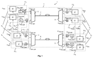
- Fig. 1 shows a schematic block diagram of an optical WDM transmission system 1.
- the optical WDM transmission system 1 comprises a transceiver device 3 i (1 ⁇ i ⁇ n) at each end of an optical link 5.
- the optical link 5 consists of two separate optical links, namely, a first optical link for a downstream transmission direction and a second optical link for an upstream transmission direction (in this description, the terms “downstream” and “upstream” are arbitrarily used in order to designate a given transmission direction without specifying any preference, especially with respect to the data rate, wherein “downstream” designates a transmission from left to right in Fig. 1 and "upstream” designates a transmission in the opposite direction).
- the first optical link comprises an optical fiber 7, a multiplexer device 11 connected, with a WDM port, to a near end of the optical fiber 7 and a demultiplexer device 15 connected, with a WDM port, to a far end of the optical fiber 7.
- the second optical link comprises an optical fiber 9, a multiplexer device 11 connected, with a WDM port, to a near end of the optical fiber 9 and a demultiplexer device 15 connected, with a WDM port, to a far end of the optical fiber 9.
- Each transceiver device 3 i comprises a transmitter device 13 i (1 ⁇ i ⁇ n) configured to create an optical channel transmit signal V TX,iopt that is supplied to a dedicated channel port of the respective multiplexer device 11.
- each transceiver device 3 i comprises a receiver device 17 i (1 ⁇ i ⁇ n) configured to receive an optical channel receive signal V RXi,opt that is output at a dedicated channel port of the respective demultiplexer device 15.
- the optical fibers 7, 9 may be standard single-mode fibers (SSMF) having usual chromatic dispersion properties (the chromatic dispersion in the 1550 nm window of an SSMF is approximately 17 ps/nm/km).
- SSMF standard single-mode fibers
- the multiplexer devices 11 and demultiplexer devices 15 of the downstream and upstream optical link may, for example, be realized as 1xn arrayed waveguide gratings (AWG).
- AWG 1xn arrayed waveguide gratings
- a single optical fiber and a single multiplexer/demultiplexer device provided at each end of the optical fiber may be used to establish the optical link 5.
- the optical signals for both transmission directions are transmitted over the single optical fiber.
- the multiplexer/demultiplexer devices may be realized as cyclic AWGs so that non-overlapping optical bands of different orders of the cyclic AWG may be used to multiplex and demultiplex downstream and upstream optical channels signals lying in respective different optical bands.
- Each optical transmitter device 13 i comprises a DMT transmitter section 19 configured to receive digital input data S TXi (1 ⁇ i ⁇ n) carrying the information to be transmitted (either in the form of an incoming digital signal or pure digital information produced by a data processing device) and to create an electrical DMT channel transmit signal S TXi,DMT (1 ⁇ i ⁇ n) to be transmitted using a given number of predetermined (electrical) carrier frequencies.
- digital input data S TXi (1 ⁇ i ⁇ n) carrying the information to be transmitted (either in the form of an incoming digital signal or pure digital information produced by a data processing device) and to create an electrical DMT channel transmit signal S TXi,DMT (1 ⁇ i ⁇ n) to be transmitted using a given number of predetermined (electrical) carrier frequencies.
- the signal transmission in the downstream direction i.e. in the direction from left to right in Fig.1
- the signal transmission in the upstream direction is effected in the same way (unless specified otherwise), wherein the reference numerals of similar signals differ by an inverted comma added to the upstream signals.
- the DMT transmitter section 19 may be configured to determine the modulation scheme that is used in each sub-channel of the DMT channel transmit signal S TXi,DMT , i.e. the set of constellation points used to create the electrical partial signals of the DMT signal by modulating the respective (electrical) sub-carrier signal having a predetermined sub-carrier frequency.
- the DMT transmitter section 19 may be configured to select the modulation scheme of the sub-channels depending on the signal-to-noise ratio (SNR) of the respective electrical partial signal of the electrical DMT (channel) receive signal S RXi,DMT which is received at the downstream end of the optical link 5.
- SNR signal-to-noise ratio
- the higher the SNR the higher the number of constellation points of the respective modulation scheme may be (i.e. the higher the number of bits assigned to a modulation symbol may be) if a given bit error rate shall be guaranteed.
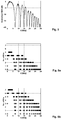
- the power spectral density (PSD) of an ideal DMT signal using the same modulation scheme in all sub-channels is shown in Fig. 2 .
- Such an ideal DMT signal would be used in case of an ideal transmission channel with no bandwidth limitation and with no or white noise added to the transmission channel.
- the spectral efficiency is excellent as the frequency-dependent power is almost homogeneously distributed over the main central portion of the bandwidth.
- the bandwidth of an optical channel defined in a transmission system can efficiently be used by using an optical DMT signal, i.e. an optical signal which is created by modulating the intensity of an optical carrier signal according to an electrical DMT signal.
- the electrical DMT signal S TXi,DMT created by the DMT transmitter section 19 is supplied to a conventional modulated optical source 21 that is configured to create an intensity-modulated optical signal S TXi,opt using the electrical DMT signal S TXi,DMT as a modulation signal.
- the modulated optical source may, for example, be realized as a directly modulated laser diode or as a CW laser diode in combination with an external optical modulator.
- the conventional optical source 21 creates an intensity-modulated signal S TXi,opt , which is a DSB optical signal, wherein the information of the modulation signal, i.e. the electrical DMT signal S TXi,DMT , is included in each of the sidebands left and right of the optical frequency of the optical carrier.
- This optical DSB signal S TXi,opt is supplied to an optical filter device 23 which is configured to at least partially suppress one of the two optical sidebands of the signal S TXi,opt .
- the signal V TXi,opt output by the optical filter device 23 is an SSB or VSB optical signal, which still carries the full information of the modulation signal S TXi,DMT in its non-suppressed sideband. Due to the at least partial suppression of one of the sidebands, the chromatic dispersion tolerance when transmitting the signal over an optical link having a predetermined chromatic dispersion is increased.
- VSB signal if not clarified otherwise.
- Each of the optical VSB channel transmit signals V TXi,opt is supplied to a dedicated channel port of the multiplexer device 11, which combines the single channel signals to a respective optical WDM transmit signal.
- the optical WDM transmit signal is output at the WDM port of the multiplexer device 11, transmitted over the downstream optical fiber 7 and received as an optical WDM receive signal at the remote end of the optical fiber 7.
- the optical WDM receive signal is demultiplexed into optical receive channel signals V RXi,opt by the optical demultiplexer device 15 coupled, at a WDM port, to the remote end of the optical fiber 7.
- Each of the single demultiplexed optical VSB channel receive signals V RXi,opt is supplied to a respective optical receiver 25 configured to convert the respective optical VSB channel receive signal V RXi,opt into an electrical DMT channel receive signal S RXi,DMT .
- Each electrical DMT channel receive signal S RXi,DMT is supplied to a DMT receiver section 27 configured to demodulate the respective DMT channel receive signal S RXi,DMT into digital output data S RXi , wherein these data may of course be output as a respective high-bit-rate signal or as pure digital data independent of a given time dependency or bit rate.
- the DMT receiver section 27 of all or selected channels may be configured to determine the SNR of the electrical partial signals comprised by the respective electrical DMT channel receive signal S RXi,DMT .
- this SNR information may be used by the respective transmitter device 13 i (which creates the respective optical channel VSB transmit signal V TX,iopt ) as a measure for allocating a suitable modulation scheme to the sub-channels of the respective electrical DMT channel transmit signal S TXi,DMT .
- this information may also be used by the transmitter device 13 i of the same transceiver device 3 i , i.e. the respective electrical DMT channel transmit signal S' TXi,DMT for creating the optical channel VSB transmit signal V' TX,iopt that is transmitted in the upstream direction is created by using the SNR information detected by the receiver device 17 i of the same transceiver device 3 i .
- the SNR information detected by a DMT receiver section 27 of a receiver device 17 i is supplied to the transmitter device 13 i of the respective transceiver device 3 i as an SNR information signal S SNRi .
- This information may be transmitted to the respective receiver device 17 i at the upstream end within a specified sub-channel of the respective electrical DMT channel transmit signal S' TXi,DMT , which serves as a control channel.
- the respective receiver device 17 i extracts the SNR information from the optical channel VSB receive signal V' RX,iopt and supplies this information, included in an SNR information signal S' SNRi , to the respective DMT transmitter section 19, which uses this information for the bit-allocation algorithm used to create the respective electrical DMT channel transmit signal S TXi,DMT .
- the DMT receiver section 27 at this upstream end of the optical link 5 may also be configured to detect an SNR information of the electrical DMT channel receive signal S' RXi,DMT and to supply this information to the respective DMT transmitter section 19 in order to transmit this information to the downstream end of the transmission link.
- the SNR information signals S' SNRi and S SNRi may include both SNR information that is detected by the respective DMT receiver section 27 for the partial signals of the electrical DMT channel receive signal S' RXi,DMT and SNR information that is included in the respective control channel of this signal.
- this different information could be supplied from the respective DMT receiver section 27 to the respective DMT transmitter section 19 using two separate signals and/or signal paths.
- the signals S' SNRi and S SNRi only include the respective SNR information that has been detected by the respective DMT receiver section 27.
- all or selected optical filter devices may be realized as variable optical filter devices, wherein the filter characteristic, i.e. especially the wavelength-dependent transmissivity of the filter device 23, can be controlled depending on a filter control information.
- the SNR "spectrum" of the electrical DMT channel receive signal S' RXi,DMT i.e. the SNR values of the partial signals of the DMT signal at the respective electrical carrier frequencies, may also be used as a measure for the (electrical) frequency responses of the transmitter device 13 i and the receiver device 17 i of a transmission link.
- this SNR information may also be used in order to determine a pre-emphasis of the respective signal components.
- this frequency range may be pre-emphasized.
- this pre-emphasis is effected in the optical domain by using an optical filter device 23 having an appropriate filter function or optical transmissivity, respectively.
- a filter control signal S Ci comprising the filter control information may be created by the DMT receiver section 27, which receives the respective SNR information from the opposite end of the transmission link or, if a symmetric transmission link can be assumed, creates the SNR information from the respective electrical DMT channel receive signal S RXi,DMT .
- This filter control signal S Ci is supplied to the respective variable optical filter device, which uses this information in order to adjust the filter properties accordingly.
- the SNR information could be supplied to the variable optical filter device 23 and the filter device 23 could be configured to create the filter control information (e.g. filter parameters) from the SNR information received.
- the optical filter devices 23 comprised by the transmitter devices 13 i provided at the upstream end of the optical link 5 are realized as variable filters only, whereas the optical filter devices 23 of the transmitter devices 13 i at the downstream end are fixed filters.
- the position of the pass band may be controllable in order to suppress a desired portion of the sideband of the respective intensity-modulated optical channel transmit signal S TXi,opt .
- the position of the pass band influences the SNR due to the chromatic dispersion sensitivity of dual-sideband optical signals (see below).
- variable optical filter device 23 a fixed filter device 23 may be used in order to create a pre-emphasized optical channel transmit signal V TXi,opt .
- Using a single optical filter in order to realize the optical filter device 23 for creating a VSB optical transmit signal which is additionally pre-emphasized in a desired manner reduces the number of components and costs for realizing the transmitter and receiver devices 13 i , 17 i .
- Using an electrical DMT channel transmit signal as a modulating signal for an optical (channel) carrier signal and creating an SSB or VSB signal by filtering the intensity-modulated optical (channel) DSB transmit signal S TXi,opt in order to create an SSB or VST optical (channel) VSB transmit signal V TXi,opt leads to an optimized use of the optical bandwidth provided by the optical link 5 for the transmission of the optical WDM signal or the optical channel signal, respectively, and to an increase in the chromatic dispersion tolerance.
- Pre-emphasizing the optical channel signals to be transmitted over the optical link 5, i.e. a pre-compensation in the optical domain avoids any reduction of the resolution during a digital-to-analog conversion in the process of creating a DMT signal as would be caused by applying a pre-compensation of bandwidth limitation (caused by a limited bandwidth of a DA converter) in the electrical digital domain.
- the (ideal) electrical DMT channel transmit signal would be created using the same modulation scheme, for example a 2 n QAM scheme, for all sub-channels. However, this would only be reasonable in case of an ideal transmission channel without bandwidth limitation and noise. In reality, however, channel bandwidth limitations apply, especially caused by the electronic components and electro-optical or opto-electrical converters provided in the transmitter device 13 i and the receiver device 17 i . Moreover, noise added to the transmission link (which comprises the optical link 5 and the respective transmitter and receiver devices 13 i , 17 i ) leads to a deterioration of its transmission properties, which can be assessed by the SNR.
- Fig. 3 shows an exemplary normalized signal-to-noise ratio "spectrum" of an electrical DMT channel receive signal S RXi,DMT measured at a receiver device 17 i of an optical transmission link similar to Fig. 1 with negligible chromatic dispersion of the optical link 5 (e.g. the optical link may be sufficiently short or comprise compensation means for sufficiently reducing the chromatic dispersion).
- the SNR for all of the plurality of sub-channels at respective discrete sub-carrier frequencies in the frequency range between 20 MHz and 30 GHz is shown.
- the roll-off of the normalized SNR for higher frequencies is caused by bandwidth limitations of the transmitter and receiver devices 13 i and 17 i . Contrary to the system in Fig.
- Fig. 3 shows the SNR "spectrum" in case of using an optical DSB signal for transporting the information of an electrical DMT channel transmit signal S RXi,DMT .
- the optical link reveals no chromatic dispersion, no power fading can be observed in Fig. 3 .
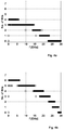
- Fig. 4 shows the number of bits assigned to each modulation symbol of the modulation schemes used in the sub-channels (which are represented by the frequencies of the electrical partial signals of the DMT signal) in case of a 56 Gb/s ( Fig. 4a ) and 112 Gb/s ( Fig. 4b ) electrical DMT channel receive signal S RXi,DMT used as modulating signal for creating the respective optical channel VSB transmit signal V TXi,opt . No optical pre-emphasis has been applied in this case.
- the SNR values measured in the sub-channels have been used as a measure for determining the modulation scheme, i.e. the number of bits assigned to each modulation symbol, in the sub-channels: the higher the SNR in the respective sub-channel, the higher the number of bits.
- Fig. 5 shows an exemplary normalized SNR "spectrum" of the sub-channels of an electrical DMT channel receive signal S RXi,DMT in a scenario similar to the scenario of Fig. 3 , wherein a predetermined non-negligible chromatic dispersion of the optical link 5 is assumed.
- the chromatic dispersion leads to power fading and, as a result, to complete drop-outs of the transmission capacity of certain sub-channels as apparent from Fig. 6 , which shows the bit allocation of the sub-channels for a 56 Bb/s ( Fig. 6a ) and a 112 Gb/s ( Fig. 6b ) electrical DMT signal.
- Fig. 9 shows two curves for an estimated SNR "spectrum" of an electrical DMT receive signal S RXi,DMT in order to visualize the effect of using an optical VSB transmit signal V TX,iopt instead.
- Curve (a) in Fig. 9 has been measured for an optical DSB transmit signal and thus shows power fading.
- Fig. 7 a situation as shown in Fig. 7 has been assumed, i.e. the optical spectrum of the optical DSB signal (the dashed curve in Fig. 7 represents the normalized rectangular optical spectrum of an ideal DMT signal; the arrow designates the optical carrier frequency) exceeds the bandwidth of the respective optical channel of the WDM system similar to the system in Fig. 1 (see the solid curve in Fig. 7 representing the normalized transmissivity of the optical channel).
- an upper frequency range of the optical DSB signal is cut off by the optical property of the optical link. This leads to a bandwidth limitation for sub-channels above approximately 22 GHz (electrical carrier frequency) as apparent from Fig. 9 .
- Curve (b) in Fig. 9 has been measured for an optical VSB transmit signal and thus shows a drastically reduced power fading effect. Especially in the frequency range above 8 GHz almost no power fading occurs. Even the first drop-out at approximately 7 GHz is extremely reduced. This is caused by the nature of the optical VSB transmit signal, which will now be explained with reference to Fig. 8 .
- the dashed curve in Fig. 8 represents the optical spectrum of the intensity-modulated optical DSB signal and the solid curve represents the transmissivity of the optical channel.
- by shifting the signal spectrum and the channel pass band relative to each other e.g.
- a separate optical filter as the filter device 23 in Fig. 1 may be used.
- the respective multiplexer device 11 may have appropriate filter properties.
- the optical sideband should be sufficiently suppressed at least for optical frequencies which are equal to or lower (if the lower sideband is suppressed) or equal to or higher (if the upper sideband is suppressed) than the optical frequency at which the first drop-out in the signal received occurs depending on the chromatic dispersion of the optical link 5.
- Figs. 10 to 12 schematically visualize the effect of an optical pre-emphasis of the optical VSB channel transmit signals that can be implemented in the system of Fig. 1 .
- Fig. 10 schematically shows the electrical spectrum of a DMT transmit signal that is used for modulating an optical source 21.
- Fig. 11 shows the optical spectrum of a respective intensity-modulated optical channel transmit signal (curve a)), wherein the arrow represents the optical carrier frequency.
- Curve (b) in Fig. 11 represents the transmissivity of an optical filter (like the filter device 23 in Fig. 1 ), which attenuates the optical frequencies remote from the optical carrier frequency less than the optical frequencies closer to the optical carrier frequency.
- Fig. 12 schematically shows the electrical spectrum of a DMT receive signal that has been transmitted by using an optical VSB signal and additionally applying an optical pre-emphasis.
- the decrease in the range of the first drop-out caused by chromatic dispersion still exists (see Fig. 9 ), while the decay at higher frequencies is compensated to a large extent.
- even a partial compensation can drastically improve the performance of a respective transmission link.
- the invention provides a method for creating an optical DMT transmission signal which makes it possible to more efficiently use the optical bandwidth provided by an optical link and to increase the chromatic dispersion tolerance by suppressing at least a relevant portion of one of the optical sidebands of an optical DSB transmit signal.
- commercial DMT transmitters may be used and operated beyond their specified operation ranges.
Landscapes
- Physics & Mathematics (AREA)
- Electromagnetism (AREA)
- Engineering & Computer Science (AREA)
- Computer Networks & Wireless Communication (AREA)
- Signal Processing (AREA)
- Optical Communication System (AREA)
Priority Applications (2)
| Application Number | Priority Date | Filing Date | Title |
|---|---|---|---|
| EP16159449.4A EP3217573B1 (fr) | 2016-03-09 | 2016-03-09 | Procédé et dispositif émetteur pour créer un signal de transmission optique |
| US15/453,102 US10270534B2 (en) | 2016-03-09 | 2017-03-08 | Method and transmitter device for creating an optical transmit signal |
Applications Claiming Priority (1)
| Application Number | Priority Date | Filing Date | Title |
|---|---|---|---|
| EP16159449.4A EP3217573B1 (fr) | 2016-03-09 | 2016-03-09 | Procédé et dispositif émetteur pour créer un signal de transmission optique |
Publications (2)
| Publication Number | Publication Date |
|---|---|
| EP3217573A1 true EP3217573A1 (fr) | 2017-09-13 |
| EP3217573B1 EP3217573B1 (fr) | 2019-09-11 |
Family
ID=55527347
Family Applications (1)
| Application Number | Title | Priority Date | Filing Date |
|---|---|---|---|
| EP16159449.4A Active EP3217573B1 (fr) | 2016-03-09 | 2016-03-09 | Procédé et dispositif émetteur pour créer un signal de transmission optique |
Country Status (2)
| Country | Link |
|---|---|
| US (1) | US10270534B2 (fr) |
| EP (1) | EP3217573B1 (fr) |
Cited By (2)
| Publication number | Priority date | Publication date | Assignee | Title |
|---|---|---|---|---|
| CN111130650A (zh) * | 2019-12-30 | 2020-05-08 | 武汉邮电科学研究院有限公司 | 强度调制直接接收的光信号生成方法、接收方法及设备 |
| EP4170935A1 (fr) * | 2021-10-19 | 2023-04-26 | Nokia Solutions and Networks Oy | Pré-accentuation numérique adaptative pour des transmissions optiques |
Families Citing this family (6)
| Publication number | Priority date | Publication date | Assignee | Title |
|---|---|---|---|---|
| GB2538793A (en) * | 2015-05-29 | 2016-11-30 | Oclaro Tech Ltd | Multiple carrier |
| JP6681217B2 (ja) * | 2016-02-29 | 2020-04-15 | 日本ルメンタム株式会社 | 光情報伝送システム、及び光送信器 |
| US10574382B2 (en) * | 2017-10-06 | 2020-02-25 | Huawei Technologies Co., Ltd. | Low cost intensity-modulated direct-detection (IMDD) optical transmitter and receiver |
| US11082132B1 (en) * | 2020-04-07 | 2021-08-03 | Bradley T Sako | Optoelectronic systems and methods for inspection of optically encoded data |
| US11671732B2 (en) * | 2020-04-07 | 2023-06-06 | Bradley T Sako | Optoelectronic systems and methods for inspection of optically encoded data |
| CN113810104B (zh) * | 2020-06-15 | 2025-03-04 | 中兴通讯股份有限公司 | 光信号处理方法、控制单元、光发射单元及存储介质 |
Citations (2)
| Publication number | Priority date | Publication date | Assignee | Title |
|---|---|---|---|---|
| US20130142520A1 (en) * | 2008-06-30 | 2013-06-06 | Chuan Xie | Anti-causal pre-emphasis for high speed optical transmission |
| EP2645599A1 (fr) * | 2012-03-29 | 2013-10-02 | Alcatel Lucent | Optimisation souple du rapport signal sur bruit pour des systèmes WDM cohérents très denses |
Family Cites Families (4)
| Publication number | Priority date | Publication date | Assignee | Title |
|---|---|---|---|---|
| US9960846B2 (en) * | 2015-07-14 | 2018-05-01 | LGS Innovations LLC | Free-space optical communication system and method in scattering environments |
| JP6613761B2 (ja) * | 2015-09-24 | 2019-12-04 | 富士通株式会社 | 光伝送システム、波長可変光フィルタの制御装置及び制御方法 |
| US9941974B2 (en) * | 2015-12-21 | 2018-04-10 | Zte Corporation | Techniques for receiving DFT spreading modulation signals |
| US10014954B2 (en) * | 2016-02-26 | 2018-07-03 | Zte Corporation | Imaging cancellation in high-speed intensity modulation and direct detection system with dual single sideband modulation |
-
2016
- 2016-03-09 EP EP16159449.4A patent/EP3217573B1/fr active Active
-
2017
- 2017-03-08 US US15/453,102 patent/US10270534B2/en active Active
Patent Citations (2)
| Publication number | Priority date | Publication date | Assignee | Title |
|---|---|---|---|---|
| US20130142520A1 (en) * | 2008-06-30 | 2013-06-06 | Chuan Xie | Anti-causal pre-emphasis for high speed optical transmission |
| EP2645599A1 (fr) * | 2012-03-29 | 2013-10-02 | Alcatel Lucent | Optimisation souple du rapport signal sur bruit pour des systèmes WDM cohérents très denses |
Non-Patent Citations (4)
| Title |
|---|
| DOCHHAN ANNIKA ET AL: "Experimental investigation of discrete multitone transmission in the presence of optical noise and chromatic dispersion", OFC 2014, OSA, 9 March 2014 (2014-03-09), pages 1 - 3, XP032633409, DOI: 10.1109/OFC.2014.6886912 * |
| DONG PO ET AL: "Four-channel vestigial sideband discrete multi-tone modulation using silicon photonic integrated circuits", 2015 EUROPEAN CONFERENCE ON OPTICAL COMMUNICATION (ECOC), VIAJES EL CORTE INGLES, VECISA, 27 September 2015 (2015-09-27), pages 1 - 3, XP032820153, DOI: 10.1109/ECOC.2015.7341850 * |
| OKABE RYO ET AL: "100 Gb/s optical discrete multi-tone transceivers for intra- and inter-datacenter networks", OPTICAL SENSING II, SPIE, 1000 20TH ST. BELLINGHAM WA 98225-6705 USA, vol. 9775, 7 March 2016 (2016-03-07), pages 97750F - 97750F, XP060069634, ISSN: 0277-786X, ISBN: 978-1-62841-971-9, DOI: 10.1117/12.2210778 * |
| T. CHAN ET AL.: "400-Gb/s Transmission Over 10-km SSMF Using Discrete Multitone and 1.3-um EML's", IEEE PHOTONICS TECHNOLOGY LETTERS, vol. 26, no. 16, 15 August 2014 (2014-08-15) |
Cited By (3)
| Publication number | Priority date | Publication date | Assignee | Title |
|---|---|---|---|---|
| CN111130650A (zh) * | 2019-12-30 | 2020-05-08 | 武汉邮电科学研究院有限公司 | 强度调制直接接收的光信号生成方法、接收方法及设备 |
| CN111130650B (zh) * | 2019-12-30 | 2020-12-29 | 武汉邮电科学研究院有限公司 | 强度调制直接接收的光信号生成方法、接收方法及设备 |
| EP4170935A1 (fr) * | 2021-10-19 | 2023-04-26 | Nokia Solutions and Networks Oy | Pré-accentuation numérique adaptative pour des transmissions optiques |
Also Published As
| Publication number | Publication date |
|---|---|
| US10270534B2 (en) | 2019-04-23 |
| US20170264368A1 (en) | 2017-09-14 |
| EP3217573B1 (fr) | 2019-09-11 |
Similar Documents
| Publication | Publication Date | Title |
|---|---|---|
| US10270534B2 (en) | Method and transmitter device for creating an optical transmit signal | |
| JP6654155B2 (ja) | 光伝送システム、ponシステムおよび伝送方法 | |
| Browning et al. | 5G wireless and wired convergence in a passive optical network using UF-OFDM and GFDM | |
| US9853728B2 (en) | Method for determining numbers of bits allocated to subcarriers and optical transmission system | |
| US20120189311A1 (en) | Optical transmission method and apparatus using ofdm | |
| JP2013514695A (ja) | 可変伝送速度を有する光ofdm伝送 | |
| US20100027994A1 (en) | Phase Modulation Of An Optical Orthogonal Frequency Division Multiplexing Signal | |
| US20150104181A1 (en) | System and method using spectral shaping and expanded channel spacing | |
| WO2005088841A1 (fr) | Systeme et procede de modulation de sous porteuse utilisee comme canal superviseur | |
| US6392770B1 (en) | Multi-point optical transmission system | |
| US20050213977A1 (en) | Split-band optical transmission system and optical transmission method used therein | |
| CN111183598B (zh) | 低成本的强度调制与直接检测(imdd)光发射器和光接收器 | |
| US10367597B2 (en) | Method and central network device for establishing an embedded optical communication channel in an optical WDM transmission system | |
| KR20170099455A (ko) | 주파수 다중화 방식 광 전송 링크에서 if 반송파의 중심 주파수를 할당하는 광 신호 전송 시스템 및 그 방법 | |
| US10090928B2 (en) | Analog optical transmission system using dispersion management technique | |
| US10419153B2 (en) | Optical transmitter and optical transmitting method | |
| EP3570469B1 (fr) | Procédé et appareil de transmission de données | |
| Chicharro et al. | Reconfigurable optical OFDM signal transmitter based on sliced ASE source for DD MB-OFDM next generation WDM access networks | |
| Llorente et al. | Impairment compensation in long-reach integrated optical-wireless PON | |
| US20060098986A1 (en) | Optical receiver for reducing optical beat interference and optical network including the optical receiver | |
| US12323185B2 (en) | Method for determining actual values of one or more characteristics of a phase-modulated optical signal | |
| EP3491751B1 (fr) | Signalisation hybride dsb et ssb | |
| Sagir et al. | 3.52 TBPS hybrid OFDM WDM PON covering 120-km long-reach distance using 4-ary QAM & direct detection technique for beyond NG-PON-2 applications | |
| KR102097893B1 (ko) | 파장 분할 다중화 송신 장치, 수신 장치와 이의 송신 방법 및 수신 방법 | |
| JPH1041886A (ja) | 光多重伝送システム |
Legal Events
| Date | Code | Title | Description |
|---|---|---|---|
| PUAI | Public reference made under article 153(3) epc to a published international application that has entered the european phase |
Free format text: ORIGINAL CODE: 0009012 |
|
| STAA | Information on the status of an ep patent application or granted ep patent |
Free format text: STATUS: THE APPLICATION HAS BEEN PUBLISHED |
|
| AK | Designated contracting states |
Kind code of ref document: A1 Designated state(s): AL AT BE BG CH CY CZ DE DK EE ES FI FR GB GR HR HU IE IS IT LI LT LU LV MC MK MT NL NO PL PT RO RS SE SI SK SM TR |
|
| AX | Request for extension of the european patent |
Extension state: BA ME |
|
| STAA | Information on the status of an ep patent application or granted ep patent |
Free format text: STATUS: REQUEST FOR EXAMINATION WAS MADE |
|
| 17P | Request for examination filed |
Effective date: 20180302 |
|
| RBV | Designated contracting states (corrected) |
Designated state(s): AL AT BE BG CH CY CZ DE DK EE ES FI FR GB GR HR HU IE IS IT LI LT LU LV MC MK MT NL NO PL PT RO RS SE SI SK SM TR |
|
| GRAP | Despatch of communication of intention to grant a patent |
Free format text: ORIGINAL CODE: EPIDOSNIGR1 |
|
| STAA | Information on the status of an ep patent application or granted ep patent |
Free format text: STATUS: GRANT OF PATENT IS INTENDED |
|
| INTG | Intention to grant announced |
Effective date: 20190405 |
|
| GRAS | Grant fee paid |
Free format text: ORIGINAL CODE: EPIDOSNIGR3 |
|
| GRAA | (expected) grant |
Free format text: ORIGINAL CODE: 0009210 |
|
| STAA | Information on the status of an ep patent application or granted ep patent |
Free format text: STATUS: THE PATENT HAS BEEN GRANTED |
|
| AK | Designated contracting states |
Kind code of ref document: B1 Designated state(s): AL AT BE BG CH CY CZ DE DK EE ES FI FR GB GR HR HU IE IS IT LI LT LU LV MC MK MT NL NO PL PT RO RS SE SI SK SM TR |
|
| REG | Reference to a national code |
Ref country code: GB Ref legal event code: FG4D |
|
| REG | Reference to a national code |
Ref country code: CH Ref legal event code: EP |
|
| REG | Reference to a national code |
Ref country code: AT Ref legal event code: REF Ref document number: 1179869 Country of ref document: AT Kind code of ref document: T Effective date: 20190915 |
|
| REG | Reference to a national code |
Ref country code: DE Ref legal event code: R096 Ref document number: 602016020225 Country of ref document: DE Ref country code: IE Ref legal event code: FG4D |
|
| REG | Reference to a national code |
Ref country code: NL Ref legal event code: MP Effective date: 20190911 |
|
| REG | Reference to a national code |
Ref country code: LT Ref legal event code: MG4D |
|
| PG25 | Lapsed in a contracting state [announced via postgrant information from national office to epo] |
Ref country code: SE Free format text: LAPSE BECAUSE OF FAILURE TO SUBMIT A TRANSLATION OF THE DESCRIPTION OR TO PAY THE FEE WITHIN THE PRESCRIBED TIME-LIMIT Effective date: 20190911 Ref country code: HR Free format text: LAPSE BECAUSE OF FAILURE TO SUBMIT A TRANSLATION OF THE DESCRIPTION OR TO PAY THE FEE WITHIN THE PRESCRIBED TIME-LIMIT Effective date: 20190911 Ref country code: LT Free format text: LAPSE BECAUSE OF FAILURE TO SUBMIT A TRANSLATION OF THE DESCRIPTION OR TO PAY THE FEE WITHIN THE PRESCRIBED TIME-LIMIT Effective date: 20190911 Ref country code: FI Free format text: LAPSE BECAUSE OF FAILURE TO SUBMIT A TRANSLATION OF THE DESCRIPTION OR TO PAY THE FEE WITHIN THE PRESCRIBED TIME-LIMIT Effective date: 20190911 Ref country code: BG Free format text: LAPSE BECAUSE OF FAILURE TO SUBMIT A TRANSLATION OF THE DESCRIPTION OR TO PAY THE FEE WITHIN THE PRESCRIBED TIME-LIMIT Effective date: 20191211 Ref country code: NO Free format text: LAPSE BECAUSE OF FAILURE TO SUBMIT A TRANSLATION OF THE DESCRIPTION OR TO PAY THE FEE WITHIN THE PRESCRIBED TIME-LIMIT Effective date: 20191211 |
|
| PG25 | Lapsed in a contracting state [announced via postgrant information from national office to epo] |
Ref country code: AL Free format text: LAPSE BECAUSE OF FAILURE TO SUBMIT A TRANSLATION OF THE DESCRIPTION OR TO PAY THE FEE WITHIN THE PRESCRIBED TIME-LIMIT Effective date: 20190911 Ref country code: ES Free format text: LAPSE BECAUSE OF FAILURE TO SUBMIT A TRANSLATION OF THE DESCRIPTION OR TO PAY THE FEE WITHIN THE PRESCRIBED TIME-LIMIT Effective date: 20190911 Ref country code: LV Free format text: LAPSE BECAUSE OF FAILURE TO SUBMIT A TRANSLATION OF THE DESCRIPTION OR TO PAY THE FEE WITHIN THE PRESCRIBED TIME-LIMIT Effective date: 20190911 Ref country code: GR Free format text: LAPSE BECAUSE OF FAILURE TO SUBMIT A TRANSLATION OF THE DESCRIPTION OR TO PAY THE FEE WITHIN THE PRESCRIBED TIME-LIMIT Effective date: 20191212 Ref country code: RS Free format text: LAPSE BECAUSE OF FAILURE TO SUBMIT A TRANSLATION OF THE DESCRIPTION OR TO PAY THE FEE WITHIN THE PRESCRIBED TIME-LIMIT Effective date: 20190911 |
|
| REG | Reference to a national code |
Ref country code: AT Ref legal event code: MK05 Ref document number: 1179869 Country of ref document: AT Kind code of ref document: T Effective date: 20190911 |
|
| PG25 | Lapsed in a contracting state [announced via postgrant information from national office to epo] |
Ref country code: PT Free format text: LAPSE BECAUSE OF FAILURE TO SUBMIT A TRANSLATION OF THE DESCRIPTION OR TO PAY THE FEE WITHIN THE PRESCRIBED TIME-LIMIT Effective date: 20200113 Ref country code: IT Free format text: LAPSE BECAUSE OF FAILURE TO SUBMIT A TRANSLATION OF THE DESCRIPTION OR TO PAY THE FEE WITHIN THE PRESCRIBED TIME-LIMIT Effective date: 20190911 Ref country code: RO Free format text: LAPSE BECAUSE OF FAILURE TO SUBMIT A TRANSLATION OF THE DESCRIPTION OR TO PAY THE FEE WITHIN THE PRESCRIBED TIME-LIMIT Effective date: 20190911 Ref country code: NL Free format text: LAPSE BECAUSE OF FAILURE TO SUBMIT A TRANSLATION OF THE DESCRIPTION OR TO PAY THE FEE WITHIN THE PRESCRIBED TIME-LIMIT Effective date: 20190911 Ref country code: EE Free format text: LAPSE BECAUSE OF FAILURE TO SUBMIT A TRANSLATION OF THE DESCRIPTION OR TO PAY THE FEE WITHIN THE PRESCRIBED TIME-LIMIT Effective date: 20190911 Ref country code: AT Free format text: LAPSE BECAUSE OF FAILURE TO SUBMIT A TRANSLATION OF THE DESCRIPTION OR TO PAY THE FEE WITHIN THE PRESCRIBED TIME-LIMIT Effective date: 20190911 Ref country code: PL Free format text: LAPSE BECAUSE OF FAILURE TO SUBMIT A TRANSLATION OF THE DESCRIPTION OR TO PAY THE FEE WITHIN THE PRESCRIBED TIME-LIMIT Effective date: 20190911 |
|
| PG25 | Lapsed in a contracting state [announced via postgrant information from national office to epo] |
Ref country code: IS Free format text: LAPSE BECAUSE OF FAILURE TO SUBMIT A TRANSLATION OF THE DESCRIPTION OR TO PAY THE FEE WITHIN THE PRESCRIBED TIME-LIMIT Effective date: 20200224 Ref country code: SM Free format text: LAPSE BECAUSE OF FAILURE TO SUBMIT A TRANSLATION OF THE DESCRIPTION OR TO PAY THE FEE WITHIN THE PRESCRIBED TIME-LIMIT Effective date: 20190911 Ref country code: SK Free format text: LAPSE BECAUSE OF FAILURE TO SUBMIT A TRANSLATION OF THE DESCRIPTION OR TO PAY THE FEE WITHIN THE PRESCRIBED TIME-LIMIT Effective date: 20190911 Ref country code: CZ Free format text: LAPSE BECAUSE OF FAILURE TO SUBMIT A TRANSLATION OF THE DESCRIPTION OR TO PAY THE FEE WITHIN THE PRESCRIBED TIME-LIMIT Effective date: 20190911 |
|
| REG | Reference to a national code |
Ref country code: DE Ref legal event code: R097 Ref document number: 602016020225 Country of ref document: DE |
|
| PLBE | No opposition filed within time limit |
Free format text: ORIGINAL CODE: 0009261 |
|
| STAA | Information on the status of an ep patent application or granted ep patent |
Free format text: STATUS: NO OPPOSITION FILED WITHIN TIME LIMIT |
|
| PG2D | Information on lapse in contracting state deleted |
Ref country code: IS |
|
| PG25 | Lapsed in a contracting state [announced via postgrant information from national office to epo] |
Ref country code: DK Free format text: LAPSE BECAUSE OF FAILURE TO SUBMIT A TRANSLATION OF THE DESCRIPTION OR TO PAY THE FEE WITHIN THE PRESCRIBED TIME-LIMIT Effective date: 20190911 Ref country code: IS Free format text: LAPSE BECAUSE OF FAILURE TO SUBMIT A TRANSLATION OF THE DESCRIPTION OR TO PAY THE FEE WITHIN THE PRESCRIBED TIME-LIMIT Effective date: 20200112 |
|
| 26N | No opposition filed |
Effective date: 20200615 |
|
| PG25 | Lapsed in a contracting state [announced via postgrant information from national office to epo] |
Ref country code: SI Free format text: LAPSE BECAUSE OF FAILURE TO SUBMIT A TRANSLATION OF THE DESCRIPTION OR TO PAY THE FEE WITHIN THE PRESCRIBED TIME-LIMIT Effective date: 20190911 |
|
| PG25 | Lapsed in a contracting state [announced via postgrant information from national office to epo] |
Ref country code: MC Free format text: LAPSE BECAUSE OF FAILURE TO SUBMIT A TRANSLATION OF THE DESCRIPTION OR TO PAY THE FEE WITHIN THE PRESCRIBED TIME-LIMIT Effective date: 20190911 |
|
| REG | Reference to a national code |
Ref country code: CH Ref legal event code: PL |
|
| REG | Reference to a national code |
Ref country code: BE Ref legal event code: MM Effective date: 20200331 |
|
| PG25 | Lapsed in a contracting state [announced via postgrant information from national office to epo] |
Ref country code: LU Free format text: LAPSE BECAUSE OF NON-PAYMENT OF DUE FEES Effective date: 20200309 |
|
| PG25 | Lapsed in a contracting state [announced via postgrant information from national office to epo] |
Ref country code: CH Free format text: LAPSE BECAUSE OF NON-PAYMENT OF DUE FEES Effective date: 20200331 Ref country code: LI Free format text: LAPSE BECAUSE OF NON-PAYMENT OF DUE FEES Effective date: 20200331 Ref country code: FR Free format text: LAPSE BECAUSE OF NON-PAYMENT OF DUE FEES Effective date: 20200331 Ref country code: IE Free format text: LAPSE BECAUSE OF NON-PAYMENT OF DUE FEES Effective date: 20200309 |
|
| PG25 | Lapsed in a contracting state [announced via postgrant information from national office to epo] |
Ref country code: BE Free format text: LAPSE BECAUSE OF NON-PAYMENT OF DUE FEES Effective date: 20200331 |
|
| PG25 | Lapsed in a contracting state [announced via postgrant information from national office to epo] |
Ref country code: TR Free format text: LAPSE BECAUSE OF FAILURE TO SUBMIT A TRANSLATION OF THE DESCRIPTION OR TO PAY THE FEE WITHIN THE PRESCRIBED TIME-LIMIT Effective date: 20190911 Ref country code: MT Free format text: LAPSE BECAUSE OF FAILURE TO SUBMIT A TRANSLATION OF THE DESCRIPTION OR TO PAY THE FEE WITHIN THE PRESCRIBED TIME-LIMIT Effective date: 20190911 Ref country code: CY Free format text: LAPSE BECAUSE OF FAILURE TO SUBMIT A TRANSLATION OF THE DESCRIPTION OR TO PAY THE FEE WITHIN THE PRESCRIBED TIME-LIMIT Effective date: 20190911 |
|
| PG25 | Lapsed in a contracting state [announced via postgrant information from national office to epo] |
Ref country code: MK Free format text: LAPSE BECAUSE OF FAILURE TO SUBMIT A TRANSLATION OF THE DESCRIPTION OR TO PAY THE FEE WITHIN THE PRESCRIBED TIME-LIMIT Effective date: 20190911 |
|
| P01 | Opt-out of the competence of the unified patent court (upc) registered |
Effective date: 20230630 |
|
| PGFP | Annual fee paid to national office [announced via postgrant information from national office to epo] |
Ref country code: DE Payment date: 20240321 Year of fee payment: 9 Ref country code: GB Payment date: 20240322 Year of fee payment: 9 |
|
| REG | Reference to a national code |
Ref country code: DE Ref legal event code: R081 Ref document number: 602016020225 Country of ref document: DE Owner name: ADTRAN NETWORKS SE, DE Free format text: FORMER OWNER: ADVA OPTICAL NETWORKING SE, 98617 MEININGEN, DE |
|
| REG | Reference to a national code |
Ref country code: DE Ref legal event code: R119 Ref document number: 602016020225 Country of ref document: DE |
|
| GBPC | Gb: european patent ceased through non-payment of renewal fee |
Effective date: 20250309 |
|
| PG25 | Lapsed in a contracting state [announced via postgrant information from national office to epo] |
Ref country code: DE Free format text: LAPSE BECAUSE OF NON-PAYMENT OF DUE FEES Effective date: 20251001 |
|
| PG25 | Lapsed in a contracting state [announced via postgrant information from national office to epo] |
Ref country code: GB Free format text: LAPSE BECAUSE OF NON-PAYMENT OF DUE FEES Effective date: 20250309 |