EP3220192A1 - Dispositif d'affichage - Google Patents
Dispositif d'affichage Download PDFInfo
- Publication number
- EP3220192A1 EP3220192A1 EP15748153.2A EP15748153A EP3220192A1 EP 3220192 A1 EP3220192 A1 EP 3220192A1 EP 15748153 A EP15748153 A EP 15748153A EP 3220192 A1 EP3220192 A1 EP 3220192A1
- Authority
- EP
- European Patent Office
- Prior art keywords
- line
- display device
- circuit board
- bonding line
- electrically connected
- Prior art date
- Legal status (The legal status is an assumption and is not a legal conclusion. Google has not performed a legal analysis and makes no representation as to the accuracy of the status listed.)
- Granted
Links
Images

Classifications
-
- G—PHYSICS
- G02—OPTICS
- G02F—OPTICAL DEVICES OR ARRANGEMENTS FOR THE CONTROL OF LIGHT BY MODIFICATION OF THE OPTICAL PROPERTIES OF THE MEDIA OF THE ELEMENTS INVOLVED THEREIN; NON-LINEAR OPTICS; FREQUENCY-CHANGING OF LIGHT; OPTICAL LOGIC ELEMENTS; OPTICAL ANALOGUE/DIGITAL CONVERTERS
- G02F1/00—Devices or arrangements for the control of the intensity, colour, phase, polarisation or direction of light arriving from an independent light source, e.g. switching, gating or modulating; Non-linear optics
- G02F1/01—Devices or arrangements for the control of the intensity, colour, phase, polarisation or direction of light arriving from an independent light source, e.g. switching, gating or modulating; Non-linear optics for the control of the intensity, phase, polarisation or colour
- G02F1/13—Devices or arrangements for the control of the intensity, colour, phase, polarisation or direction of light arriving from an independent light source, e.g. switching, gating or modulating; Non-linear optics for the control of the intensity, phase, polarisation or colour based on liquid crystals, e.g. single liquid crystal display cells
- G02F1/133—Constructional arrangements; Operation of liquid crystal cells; Circuit arrangements
- G02F1/1333—Constructional arrangements; Manufacturing methods
- G02F1/1345—Conductors connecting electrodes to cell terminals
-
- G—PHYSICS
- G02—OPTICS
- G02F—OPTICAL DEVICES OR ARRANGEMENTS FOR THE CONTROL OF LIGHT BY MODIFICATION OF THE OPTICAL PROPERTIES OF THE MEDIA OF THE ELEMENTS INVOLVED THEREIN; NON-LINEAR OPTICS; FREQUENCY-CHANGING OF LIGHT; OPTICAL LOGIC ELEMENTS; OPTICAL ANALOGUE/DIGITAL CONVERTERS
- G02F1/00—Devices or arrangements for the control of the intensity, colour, phase, polarisation or direction of light arriving from an independent light source, e.g. switching, gating or modulating; Non-linear optics
- G02F1/01—Devices or arrangements for the control of the intensity, colour, phase, polarisation or direction of light arriving from an independent light source, e.g. switching, gating or modulating; Non-linear optics for the control of the intensity, phase, polarisation or colour
- G02F1/13—Devices or arrangements for the control of the intensity, colour, phase, polarisation or direction of light arriving from an independent light source, e.g. switching, gating or modulating; Non-linear optics for the control of the intensity, phase, polarisation or colour based on liquid crystals, e.g. single liquid crystal display cells
- G02F1/133—Constructional arrangements; Operation of liquid crystal cells; Circuit arrangements
- G02F1/1333—Constructional arrangements; Manufacturing methods
- G02F1/1335—Structural association of cells with optical devices, e.g. polarisers or reflectors
- G02F1/133509—Filters, e.g. light shielding masks
- G02F1/133512—Light shielding layers, e.g. black matrix
-
- G—PHYSICS
- G02—OPTICS
- G02F—OPTICAL DEVICES OR ARRANGEMENTS FOR THE CONTROL OF LIGHT BY MODIFICATION OF THE OPTICAL PROPERTIES OF THE MEDIA OF THE ELEMENTS INVOLVED THEREIN; NON-LINEAR OPTICS; FREQUENCY-CHANGING OF LIGHT; OPTICAL LOGIC ELEMENTS; OPTICAL ANALOGUE/DIGITAL CONVERTERS
- G02F1/00—Devices or arrangements for the control of the intensity, colour, phase, polarisation or direction of light arriving from an independent light source, e.g. switching, gating or modulating; Non-linear optics
- G02F1/01—Devices or arrangements for the control of the intensity, colour, phase, polarisation or direction of light arriving from an independent light source, e.g. switching, gating or modulating; Non-linear optics for the control of the intensity, phase, polarisation or colour
- G02F1/13—Devices or arrangements for the control of the intensity, colour, phase, polarisation or direction of light arriving from an independent light source, e.g. switching, gating or modulating; Non-linear optics for the control of the intensity, phase, polarisation or colour based on liquid crystals, e.g. single liquid crystal display cells
- G02F1/133—Constructional arrangements; Operation of liquid crystal cells; Circuit arrangements
- G02F1/1333—Constructional arrangements; Manufacturing methods
- G02F1/1339—Gaskets; Spacers; Sealing of cells
-
- G—PHYSICS
- G02—OPTICS
- G02F—OPTICAL DEVICES OR ARRANGEMENTS FOR THE CONTROL OF LIGHT BY MODIFICATION OF THE OPTICAL PROPERTIES OF THE MEDIA OF THE ELEMENTS INVOLVED THEREIN; NON-LINEAR OPTICS; FREQUENCY-CHANGING OF LIGHT; OPTICAL LOGIC ELEMENTS; OPTICAL ANALOGUE/DIGITAL CONVERTERS
- G02F1/00—Devices or arrangements for the control of the intensity, colour, phase, polarisation or direction of light arriving from an independent light source, e.g. switching, gating or modulating; Non-linear optics
- G02F1/01—Devices or arrangements for the control of the intensity, colour, phase, polarisation or direction of light arriving from an independent light source, e.g. switching, gating or modulating; Non-linear optics for the control of the intensity, phase, polarisation or colour
- G02F1/13—Devices or arrangements for the control of the intensity, colour, phase, polarisation or direction of light arriving from an independent light source, e.g. switching, gating or modulating; Non-linear optics for the control of the intensity, phase, polarisation or colour based on liquid crystals, e.g. single liquid crystal display cells
- G02F1/133—Constructional arrangements; Operation of liquid crystal cells; Circuit arrangements
- G02F1/1333—Constructional arrangements; Manufacturing methods
- G02F1/1341—Filling or closing of cells
-
- G—PHYSICS
- G02—OPTICS
- G02F—OPTICAL DEVICES OR ARRANGEMENTS FOR THE CONTROL OF LIGHT BY MODIFICATION OF THE OPTICAL PROPERTIES OF THE MEDIA OF THE ELEMENTS INVOLVED THEREIN; NON-LINEAR OPTICS; FREQUENCY-CHANGING OF LIGHT; OPTICAL LOGIC ELEMENTS; OPTICAL ANALOGUE/DIGITAL CONVERTERS
- G02F1/00—Devices or arrangements for the control of the intensity, colour, phase, polarisation or direction of light arriving from an independent light source, e.g. switching, gating or modulating; Non-linear optics
- G02F1/01—Devices or arrangements for the control of the intensity, colour, phase, polarisation or direction of light arriving from an independent light source, e.g. switching, gating or modulating; Non-linear optics for the control of the intensity, phase, polarisation or colour
- G02F1/13—Devices or arrangements for the control of the intensity, colour, phase, polarisation or direction of light arriving from an independent light source, e.g. switching, gating or modulating; Non-linear optics for the control of the intensity, phase, polarisation or colour based on liquid crystals, e.g. single liquid crystal display cells
- G02F1/133—Constructional arrangements; Operation of liquid crystal cells; Circuit arrangements
- G02F1/1333—Constructional arrangements; Manufacturing methods
- G02F1/1345—Conductors connecting electrodes to cell terminals
- G02F1/13452—Conductors connecting driver circuitry and terminals of panels
-
- G—PHYSICS
- G02—OPTICS
- G02F—OPTICAL DEVICES OR ARRANGEMENTS FOR THE CONTROL OF LIGHT BY MODIFICATION OF THE OPTICAL PROPERTIES OF THE MEDIA OF THE ELEMENTS INVOLVED THEREIN; NON-LINEAR OPTICS; FREQUENCY-CHANGING OF LIGHT; OPTICAL LOGIC ELEMENTS; OPTICAL ANALOGUE/DIGITAL CONVERTERS
- G02F1/00—Devices or arrangements for the control of the intensity, colour, phase, polarisation or direction of light arriving from an independent light source, e.g. switching, gating or modulating; Non-linear optics
- G02F1/01—Devices or arrangements for the control of the intensity, colour, phase, polarisation or direction of light arriving from an independent light source, e.g. switching, gating or modulating; Non-linear optics for the control of the intensity, phase, polarisation or colour
- G02F1/13—Devices or arrangements for the control of the intensity, colour, phase, polarisation or direction of light arriving from an independent light source, e.g. switching, gating or modulating; Non-linear optics for the control of the intensity, phase, polarisation or colour based on liquid crystals, e.g. single liquid crystal display cells
- G02F1/133—Constructional arrangements; Operation of liquid crystal cells; Circuit arrangements
- G02F1/1333—Constructional arrangements; Manufacturing methods
- G02F1/1345—Conductors connecting electrodes to cell terminals
- G02F1/13458—Terminal pads
-
- G—PHYSICS
- G02—OPTICS
- G02F—OPTICAL DEVICES OR ARRANGEMENTS FOR THE CONTROL OF LIGHT BY MODIFICATION OF THE OPTICAL PROPERTIES OF THE MEDIA OF THE ELEMENTS INVOLVED THEREIN; NON-LINEAR OPTICS; FREQUENCY-CHANGING OF LIGHT; OPTICAL LOGIC ELEMENTS; OPTICAL ANALOGUE/DIGITAL CONVERTERS
- G02F1/00—Devices or arrangements for the control of the intensity, colour, phase, polarisation or direction of light arriving from an independent light source, e.g. switching, gating or modulating; Non-linear optics
- G02F1/01—Devices or arrangements for the control of the intensity, colour, phase, polarisation or direction of light arriving from an independent light source, e.g. switching, gating or modulating; Non-linear optics for the control of the intensity, phase, polarisation or colour
- G02F1/13—Devices or arrangements for the control of the intensity, colour, phase, polarisation or direction of light arriving from an independent light source, e.g. switching, gating or modulating; Non-linear optics for the control of the intensity, phase, polarisation or colour based on liquid crystals, e.g. single liquid crystal display cells
- G02F1/133—Constructional arrangements; Operation of liquid crystal cells; Circuit arrangements
- G02F1/136—Liquid crystal cells structurally associated with a semi-conducting layer or substrate, e.g. cells forming part of an integrated circuit
- G02F1/1362—Active matrix addressed cells
- G02F1/136209—Light shielding layers, e.g. black matrix, incorporated in the active matrix substrate, e.g. structurally associated with the switching element
-
- G—PHYSICS
- G02—OPTICS
- G02F—OPTICAL DEVICES OR ARRANGEMENTS FOR THE CONTROL OF LIGHT BY MODIFICATION OF THE OPTICAL PROPERTIES OF THE MEDIA OF THE ELEMENTS INVOLVED THEREIN; NON-LINEAR OPTICS; FREQUENCY-CHANGING OF LIGHT; OPTICAL LOGIC ELEMENTS; OPTICAL ANALOGUE/DIGITAL CONVERTERS
- G02F1/00—Devices or arrangements for the control of the intensity, colour, phase, polarisation or direction of light arriving from an independent light source, e.g. switching, gating or modulating; Non-linear optics
- G02F1/01—Devices or arrangements for the control of the intensity, colour, phase, polarisation or direction of light arriving from an independent light source, e.g. switching, gating or modulating; Non-linear optics for the control of the intensity, phase, polarisation or colour
- G02F1/13—Devices or arrangements for the control of the intensity, colour, phase, polarisation or direction of light arriving from an independent light source, e.g. switching, gating or modulating; Non-linear optics for the control of the intensity, phase, polarisation or colour based on liquid crystals, e.g. single liquid crystal display cells
- G02F1/133—Constructional arrangements; Operation of liquid crystal cells; Circuit arrangements
- G02F1/136—Liquid crystal cells structurally associated with a semi-conducting layer or substrate, e.g. cells forming part of an integrated circuit
- G02F1/1362—Active matrix addressed cells
- G02F1/136286—Wiring, e.g. gate line, drain line
-
- G—PHYSICS
- G09—EDUCATION; CRYPTOGRAPHY; DISPLAY; ADVERTISING; SEALS
- G09G—ARRANGEMENTS OR CIRCUITS FOR CONTROL OF INDICATING DEVICES USING STATIC MEANS TO PRESENT VARIABLE INFORMATION
- G09G3/00—Control arrangements or circuits, of interest only in connection with visual indicators other than cathode-ray tubes
- G09G3/20—Control arrangements or circuits, of interest only in connection with visual indicators other than cathode-ray tubes for presentation of an assembly of a number of characters, e.g. a page, by composing the assembly by combination of individual elements arranged in a matrix no fixed position being assigned to or needed to be assigned to the individual characters or partial characters
- G09G3/34—Control arrangements or circuits, of interest only in connection with visual indicators other than cathode-ray tubes for presentation of an assembly of a number of characters, e.g. a page, by composing the assembly by combination of individual elements arranged in a matrix no fixed position being assigned to or needed to be assigned to the individual characters or partial characters by control of light from an independent source
- G09G3/36—Control arrangements or circuits, of interest only in connection with visual indicators other than cathode-ray tubes for presentation of an assembly of a number of characters, e.g. a page, by composing the assembly by combination of individual elements arranged in a matrix no fixed position being assigned to or needed to be assigned to the individual characters or partial characters by control of light from an independent source using liquid crystals
- G09G3/3611—Control of matrices with row and column drivers
- G09G3/3648—Control of matrices with row and column drivers using an active matrix
- G09G3/3655—Details of drivers for counter electrodes, e.g. common electrodes for pixel capacitors or supplementary storage capacitors
-
- H—ELECTRICITY
- H01—ELECTRIC ELEMENTS
- H01B—CABLES; CONDUCTORS; INSULATORS; SELECTION OF MATERIALS FOR THEIR CONDUCTIVE, INSULATING OR DIELECTRIC PROPERTIES
- H01B1/00—Conductors or conductive bodies characterised by the conductive materials; Selection of materials as conductors
- H01B1/02—Conductors or conductive bodies characterised by the conductive materials; Selection of materials as conductors mainly consisting of metals or alloys
-
- H—ELECTRICITY
- H05—ELECTRIC TECHNIQUES NOT OTHERWISE PROVIDED FOR
- H05K—PRINTED CIRCUITS; CASINGS OR CONSTRUCTIONAL DETAILS OF ELECTRIC APPARATUS; MANUFACTURE OF ASSEMBLAGES OF ELECTRICAL COMPONENTS
- H05K1/00—Printed circuits
- H05K1/02—Details
- H05K1/0277—Bendability or stretchability details
- H05K1/028—Bending or folding regions of flexible printed circuits
-
- H—ELECTRICITY
- H10—SEMICONDUCTOR DEVICES; ELECTRIC SOLID-STATE DEVICES NOT OTHERWISE PROVIDED FOR
- H10D—INORGANIC ELECTRIC SEMICONDUCTOR DEVICES
- H10D86/00—Integrated devices formed in or on insulating or conducting substrates, e.g. formed in silicon-on-insulator [SOI] substrates or on stainless steel or glass substrates
- H10D86/40—Integrated devices formed in or on insulating or conducting substrates, e.g. formed in silicon-on-insulator [SOI] substrates or on stainless steel or glass substrates characterised by multiple TFTs
- H10D86/441—Interconnections, e.g. scanning lines
- H10D86/443—Interconnections, e.g. scanning lines adapted for preventing breakage, peeling or short circuiting
-
- H—ELECTRICITY
- H10—SEMICONDUCTOR DEVICES; ELECTRIC SOLID-STATE DEVICES NOT OTHERWISE PROVIDED FOR
- H10D—INORGANIC ELECTRIC SEMICONDUCTOR DEVICES
- H10D86/00—Integrated devices formed in or on insulating or conducting substrates, e.g. formed in silicon-on-insulator [SOI] substrates or on stainless steel or glass substrates
- H10D86/40—Integrated devices formed in or on insulating or conducting substrates, e.g. formed in silicon-on-insulator [SOI] substrates or on stainless steel or glass substrates characterised by multiple TFTs
- H10D86/60—Integrated devices formed in or on insulating or conducting substrates, e.g. formed in silicon-on-insulator [SOI] substrates or on stainless steel or glass substrates characterised by multiple TFTs wherein the TFTs are in active matrices
-
- G—PHYSICS
- G02—OPTICS
- G02F—OPTICAL DEVICES OR ARRANGEMENTS FOR THE CONTROL OF LIGHT BY MODIFICATION OF THE OPTICAL PROPERTIES OF THE MEDIA OF THE ELEMENTS INVOLVED THEREIN; NON-LINEAR OPTICS; FREQUENCY-CHANGING OF LIGHT; OPTICAL LOGIC ELEMENTS; OPTICAL ANALOGUE/DIGITAL CONVERTERS
- G02F1/00—Devices or arrangements for the control of the intensity, colour, phase, polarisation or direction of light arriving from an independent light source, e.g. switching, gating or modulating; Non-linear optics
- G02F1/01—Devices or arrangements for the control of the intensity, colour, phase, polarisation or direction of light arriving from an independent light source, e.g. switching, gating or modulating; Non-linear optics for the control of the intensity, phase, polarisation or colour
- G02F1/13—Devices or arrangements for the control of the intensity, colour, phase, polarisation or direction of light arriving from an independent light source, e.g. switching, gating or modulating; Non-linear optics for the control of the intensity, phase, polarisation or colour based on liquid crystals, e.g. single liquid crystal display cells
- G02F1/133—Constructional arrangements; Operation of liquid crystal cells; Circuit arrangements
- G02F1/136—Liquid crystal cells structurally associated with a semi-conducting layer or substrate, e.g. cells forming part of an integrated circuit
- G02F1/1362—Active matrix addressed cells
- G02F1/136222—Colour filters incorporated in the active matrix substrate
Definitions
- the present disclosure relates to the field of display technology, in particular to a display device.
- a liquid crystal display device is a flat, super-thin display device, which has advantages such as being of small volume, small thickness, light weight, low energy consumption and low radiation.
- the liquid crystal display device includes a color filter substrate and an array substrate.
- the color filter substrate may include a display region, a peripheral black matrix region and a process reserved blank region.
- the array substrate may include a display region and a peripheral wiring region.
- structures such as gate lines, data lines, thin film transistors (TFTs) and pixel electrodes are provided.
- data line bonding lines and gate line bonding lines are provided.
- the data line bonding line is configured to transmit a data signal outputted by a source driving circuit to the data line
- the gate line bonding line is configured to transmit a gate driving signal outputted by a gate driving circuit to the gate line so as to drive structures such as TFTs and the pixel electrodes within the display region to work, thereby to enable the display region to display images.
- LCD liquid crystal display
- An object of the present disclosure is to provide a display device having a narrower bezel.
- the present disclosure provides in one embodiment a display device, including an array substrate and a color filter substrate.
- the color filter substrate includes a display region, a peripheral black matrix region and a process reserved blank region which are sequentially arranged from inside to outside.
- a bonding line is provided within the peripheral black matrix region and/or the process reserved blank region and electrically connected to a structure to be bonded on the array substrate through a connection structure.
- the display region is provided with a common electrode
- the bonding line and the common electrode are of an identical material and arranged in an identical layer.
- the material of the common electrode is indium tin oxide.
- the display device further includes a sealant which makes the array substrate adhere to the color filter substrate.
- the sealant contains metal balls used as the connection structure, and the connection structure contains at least one metal ball at a position corresponding to each bonding line.
- connection structure includes one metal ball at a position corresponding to each bonding line.
- the metal balls each has a diameter of 2-5 ⁇ m.
- the structure to be bonded is provided with a conductive pad, a material of the conductive pad is indium tin oxide, the connection structure is electrically connected to the structure to be bonded through the conductive pad.
- the structure to be bonded includes a gate line and a data line, the bonding line includes a gate line bonding line and a data line bonding line; or the structure to be bonded includes a gate line, the bonding line includes a gate line bonding line; or the structure to be bonded includes a data line, the bonding line includes a data line bonding line.
- the conductive pad includes a gate line conductive pad and/or a data line conductive pad.
- the gate line conductive pad is electrically connected to the gate line via a first via hole in a gate insulation layer arranged on the gate line
- the data line conductive pad is electrically connected to the data line via a second via hole in a passivation layer arranged on the data line.
- the gate line conductive pad arranged on the first via hole and the data line conductive pad arranged on the second via hole are each provided with a groove.
- the display device further includes a flexible circuit board and a printed circuit board, the bonding line is electrically connected to a driving circuit on the printed circuit board through the flexible circuit board.
- the flexible circuit board includes: a first connecting finger arranged on one surface of the flexible circuit board and a second connecting finger arranged on the other surface of the flexible circuit board.
- the first connecting finger is electrically connected to the bonding line
- the second connecting finger is electrically connected to the driving circuit on the printed circuit board.
- the flexible circuit board includes a first connecting finger and a second connecting finger which are arranged respectively on two ends of a same surface of the flexible circuit board; and the flexible circuit board is bent so that the first connecting finger is electrically connected to the driving circuit on the printed circuit board and the second connecting finger is electrically connected to the bonding line.
- one end of the bonding line is electrically connected to the driving circuit of the printed circuit board through the flexible circuit board, and the other end of the bonding line is electrically connected to the structure to be bonded through the connection structure.
- the present disclosure provides a display device.
- the display device includes an array substrate and a color filter substrate.
- the color filter substrate includes a display region, a peripheral black matrix region and a process reserved blank region which are sequentially arranged from inside to outside.
- a bonding line is provided within the peripheral black matrix region and/or the process reserved blank region and electrically connected to a structure to be bonded on the array substrate through a connection structure. Therefore, the existing regions on the color filter substrate are fully used, thereby avoiding arrangement of the bonding line on the array substrate, so as to enable the display device to have a narrow bezel.
- the present disclosure provides a display device which has a narrow bezel.
- the display device includes a color filter substrate and an array substrate.
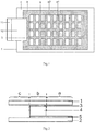
- the color filter substrate 1 includes a display region a, a peripheral black matrix region b and a process reserved blank region c, which are arranged sequentially from inside to outside.
- a bonding line 3 is provided within the peripheral black matrix region b and/or the process reserved blank region c.
- the bonding line 3 is electrically connected to a structure to be bonded 5 on the array substrate 2 through a connection structure 4.
- connection structure 4 may be a metal ball in sealant or a conductive structure such as a conductive adhesive.
- the color filter substrate 1 generally further includes structures such as a black matrix a1 and a color filter layer a2 in the display region a, so as to achieve a color display of the display device.
- a peripheral black matrix is provided within the peripheral black matrix region b so as to prevent light leakage from an edge of the display device.
- the peripheral black matrix and the black matrix a1 in the display region a may be of an identical material and formed simultaneously.
- the process reserved blank region c is used to prevent the structures such as the black matrix a1 and the color filter layer a2 in the display region a on the color filter substrate 1 from being damaged during a cutting process when forming a liquid crystal cell.
- the bonding line 3 may be arranged in the peripheral black matrix region b.
- the bonding line 3 can be extended to the process reserved blank region c, so as to prevent the bonding line 3 from being damaged during the cutting process when forming the liquid crystal cell.
- the display region a may be provided with a transparent conductive common electrode.
- the common electrode is arranged on the black matrix a1 and the color filter layer a2.
- the bonding line 3 and the common electrode may be of an identical material and arranged in an identical layer.
- the material of the common electrode may be indium tin oxide (ITO).
- the display device may further include a sealant 6 which is configured to make the color filter substrate 1 adhere to the array substrate 2.
- the sealant 6 contains a metal ball which is used as the connection structure 4, and the connection structure contains at least one metal ball at a position corresponding to each bonding line 3.
- the metal ball(s) in the sealant 6 may be mixed into the sealant 6 through the following way: placing a certain amount of metal balls into a sealant 6 which is in a sticky state; stirring for a certain period of time at a certain speed and at a suitable temperature, so that a sealant 6 in a sticky state and containing metal balls can be obtained; then coating the sealant 6 in the sticky state onto a peripheral region of the array substrate 2 or the color filter substrate 1; curing the sealant 6 by UV irradiation, so that the sealant 6 in which the metal balls are uniformly distributed is obtained. No metal ball is in contact with each other.
- connection structure 4 includes one metal ball
- the metal ball in one embodiment has a diameter of, for example, 2-5 ⁇ m.
- metal balls in the sealant 6 must be in no contact with each other, so as to avoid connection of two adjacent bonding lines 3 or two adjacent structures to be bonded 5.
- the structure to be bonded 5 on the array substrate 2 may include a gate line and/or a data line, a material of which is usually metal. Since oxidation resistance of metal is poor, thus, as shown in Fig.3 and Fig.4 , in one embodiment of the present disclosure, the structure to be bonded 5 may be provided with a conductive pad 7.
- the conductive pad 7 is of a material of indium tin oxide (ITO).
- ITO indium tin oxide
- the structure to be bonded 5 may include a gate line and a data line; correspondingly, the bonding line 3 includes a gate line bonding line and a data line bonding line.
- the structure to be bonded 5 may also include a gate line; correspondingly, the bonding line 3 includes a gate line bonding line.
- the structure to be bonded 5 may further include a data line; correspondingly, the bonding line 3 includes a data line bonding line.
- the structure to be bonded 5 includes the data line, and the bonding line 3 includes the data line bonding line.
- the conductive pad 7 may include a gate line conductive pad and/or a data line conductive pad.
- the structure to be bonded 5 is a gate line
- the bonding line 3 is a gate line bonding line.
- the conductive pad 7 is a gate line conductive pad, and electrically connected to the gate line via a first via hole 81 in a gate insulation layer 8 arranged on the gate line.
- the structure to be bonded 5 is a data line
- the bonding line 3 is a data line bonding line.
- the conductive pad 7 is a data line conductive pad, and electrically connected to the data line via a second via hole 91 in a passivation layer 9 arranged on the data line.
- the gate line conductive pad arranged on the first via hole 81 is provided with a groove.
- the data line conductive pad arranged on the second via hole 91 is also provided with a groove.
- the groove helps to fix the metal ball, so as to further ensure an electrical connection between the gate line on the array substrate 2 and the gate line bonding line on the color filter substrate 1 at a position right corresponding to the gate line, and an electrical connection between the data line on the array substrate 2 and the data line bonding line on the color filter substrate 1 at a position right corresponding to the data line.
- the display device further includes a flexible circuit board 10 and a printed circuit board 11.
- the bonding line 3 is electrically connected to a driving circuit on the printed circuit board 11 through the flexible circuit board 10.
- one end of the bonding line 3 is electrically connected to the driving circuit of the printed circuit board 11 through the flexible circuit board 10
- the other end of the bonding line 3 is electrically connected to the structure to be bonded 5 through the connection structure 4, so as to enable to transmit a drive signal outputted by the driving circuit on the printed circuit board 11 to the structure to be bonded 5.
- the electrical connection between the bonding line 3 and the driving circuit of the printed circuit board 11 may achieve through the flexible circuit board 10 which has one of the following two structures.
- the flexible circuit board 10 includes a first connecting finger and a second connecting finger, which are arranged on two ends of a same surface of the flexible circuit board 10; the flexible circuit board 10 is bent so that the first connecting finger is electrically connected to the driving circuit on the printed circuit board 11 and the second connecting finger is electrically connected to the bonding line 3, thereby achieving the electrical connection between the bonding line 3 and the driving circuit of the printed circuit board 11.
- the flexible circuit board 10 includes a first connecting finger arranged on one surface of the flexible circuit board 10 and a second connecting finger arranged on the other surface of the flexible circuit board 10; the first connecting finger is electrically connected to the bonding line 3, and the second connecting finger is electrically connected to the driving circuit on the printed circuit board 11; at this point, the electrical connection between the bonding line 3 and the driving circuit of the printed circuit board 11 can be achieved without bending the flexible circuit board 10; as a result, an assembly of the display device is convenient and a space can be saved.
- the present disclosure provides in one embodiment a display device.
- the display device includes an array substrate and a color filter substrate.
- the color filter substrate includes a display region, a peripheral black matrix region and a process reserved blank region which are sequentially arranged from inside to outside.
- a bonding line is provided within the peripheral black matrix region and/or the process reserved blank region and electrically connected to a structure to be bonded on the array substrate through a connection structure. Therefore, the existing regions on the color filter substrate are fully used, thereby avoiding arrangement of the bonding line on the array substrate, so as to enable the display device to have a narrow bezel.
Landscapes
- Physics & Mathematics (AREA)
- Nonlinear Science (AREA)
- Crystallography & Structural Chemistry (AREA)
- General Physics & Mathematics (AREA)
- Chemical & Material Sciences (AREA)
- Mathematical Physics (AREA)
- Optics & Photonics (AREA)
- Engineering & Computer Science (AREA)
- Microelectronics & Electronic Packaging (AREA)
- Devices For Indicating Variable Information By Combining Individual Elements (AREA)
- Power Engineering (AREA)
- Computer Hardware Design (AREA)
- Theoretical Computer Science (AREA)
- Liquid Crystal (AREA)
Applications Claiming Priority (2)
| Application Number | Priority Date | Filing Date | Title |
|---|---|---|---|
| CN201410640405.1A CN104317125A (zh) | 2014-11-13 | 2014-11-13 | 一种显示装置 |
| PCT/CN2015/073345 WO2016074375A1 (fr) | 2014-11-13 | 2015-02-27 | Dispositif d'affichage |
Publications (3)
| Publication Number | Publication Date |
|---|---|
| EP3220192A1 true EP3220192A1 (fr) | 2017-09-20 |
| EP3220192A4 EP3220192A4 (fr) | 2018-06-27 |
| EP3220192B1 EP3220192B1 (fr) | 2019-09-11 |
Family
ID=52372376
Family Applications (1)
| Application Number | Title | Priority Date | Filing Date |
|---|---|---|---|
| EP15748153.2A Active EP3220192B1 (fr) | 2014-11-13 | 2015-02-27 | Dispositif d'affichage |
Country Status (6)
| Country | Link |
|---|---|
| US (1) | US9954012B2 (fr) |
| EP (1) | EP3220192B1 (fr) |
| JP (1) | JP2018501525A (fr) |
| KR (1) | KR101728787B1 (fr) |
| CN (1) | CN104317125A (fr) |
| WO (1) | WO2016074375A1 (fr) |
Families Citing this family (8)
| Publication number | Priority date | Publication date | Assignee | Title |
|---|---|---|---|---|
| CN104317125A (zh) | 2014-11-13 | 2015-01-28 | 合肥鑫晟光电科技有限公司 | 一种显示装置 |
| CN106157818B (zh) * | 2016-09-05 | 2022-06-24 | 京东方科技集团股份有限公司 | 一种柔性显示面板、其制作方法及显示装置 |
| CN106571103A (zh) * | 2016-10-27 | 2017-04-19 | 昆山国显光电有限公司 | 一种邦定结构及其应用 |
| CN108777114B (zh) * | 2018-06-26 | 2021-05-14 | 上海中航光电子有限公司 | 显示面板及其制造方法、显示装置和拼接屏 |
| CN109239991B (zh) | 2018-10-10 | 2021-01-08 | 惠科股份有限公司 | 一种显示面板的制程和显示面板 |
| CN109358459B (zh) * | 2018-11-09 | 2020-11-24 | 惠科股份有限公司 | 一种显示面板、制作方法和显示装置 |
| CN110967878A (zh) * | 2019-10-22 | 2020-04-07 | 武汉华星光电技术有限公司 | 一种窄边框液晶显示面板及其制造方法 |
| CN111755463A (zh) * | 2020-06-24 | 2020-10-09 | 武汉华星光电半导体显示技术有限公司 | 显示面板及显示装置 |
Family Cites Families (24)
| Publication number | Priority date | Publication date | Assignee | Title |
|---|---|---|---|---|
| JPH05165060A (ja) * | 1991-12-17 | 1993-06-29 | Sony Corp | 液晶表示装置 |
| JP3708770B2 (ja) | 1999-12-24 | 2005-10-19 | セイコーエプソン株式会社 | 液晶装置の製造方法 |
| JP2002049034A (ja) | 2000-05-25 | 2002-02-15 | Seiko Epson Corp | 液晶装置、その製造方法および電子機器 |
| JP2001350422A (ja) * | 2000-06-08 | 2001-12-21 | Matsushita Electric Ind Co Ltd | 電子機器用表示装置 |
| US7050131B2 (en) * | 2002-10-17 | 2006-05-23 | Lg.Philips Lcd Co., Ltd. | Liquid crystal display device having black seal pattern and external resin pattern, and method of fabricating the same |
| JP4593161B2 (ja) * | 2004-04-30 | 2010-12-08 | 三菱電機株式会社 | 液晶表示装置 |
| KR20070005236A (ko) * | 2005-07-05 | 2007-01-10 | 삼성전자주식회사 | 액정 표시 장치 |
| KR101146527B1 (ko) * | 2005-11-30 | 2012-05-25 | 엘지디스플레이 주식회사 | 게이트 인 패널 구조 액정표시장치 및 그 제조 방법 |
| CN101359108A (zh) | 2007-07-31 | 2009-02-04 | 北京京东方光电科技有限公司 | 薄膜晶体管液晶显示器面板结构 |
| KR20100019666A (ko) * | 2008-08-11 | 2010-02-19 | 삼성전자주식회사 | 박막 트랜지스터 표시판, 이를 포함하는 액정 표시 장치, 그리고 액정 표시 장치의 제조 방법 |
| CN101676776B (zh) * | 2008-09-16 | 2012-02-29 | 北京京东方光电科技有限公司 | 面板及面板的制造方法 |
| KR20100041165A (ko) * | 2008-10-13 | 2010-04-22 | 삼성전자주식회사 | 표시 장치 및 그를 포함하는 멀티 표시 장치 |
| CN102193236A (zh) * | 2010-03-02 | 2011-09-21 | 京东方科技集团股份有限公司 | 彩膜基板及其制造方法 |
| CN101957522B (zh) * | 2010-09-01 | 2013-03-13 | 友达光电股份有限公司 | 显示面板 |
| CN201909918U (zh) * | 2010-12-30 | 2011-07-27 | 京东方科技集团股份有限公司 | 液晶面板检测装置 |
| JP2012220792A (ja) * | 2011-04-11 | 2012-11-12 | Japan Display East Co Ltd | 液晶表示装置及び液晶表示装置製造方法 |
| KR101356594B1 (ko) * | 2011-11-11 | 2014-02-05 | 엘지디스플레이 주식회사 | 액정표시장치 |
| CN103293736B (zh) * | 2012-09-05 | 2015-12-16 | 上海天马微电子有限公司 | 内嵌式液晶触控面板 |
| CN103293750B (zh) * | 2012-12-14 | 2016-05-11 | 上海天马微电子有限公司 | 一种内嵌式触摸屏彩膜基板及其制造方法 |
| CN103116233B (zh) * | 2013-01-23 | 2016-01-06 | 北京京东方光电科技有限公司 | 一种触摸液晶光栅结构及3d触摸显示装置 |
| KR102077143B1 (ko) * | 2013-05-30 | 2020-02-14 | 삼성디스플레이 주식회사 | 유기 발광 표시 장치 및 그 제조 방법 |
| CN103885221B (zh) * | 2014-04-14 | 2017-05-03 | 深圳市华星光电技术有限公司 | 大板加电线路及其制造方法 |
| CN104317125A (zh) * | 2014-11-13 | 2015-01-28 | 合肥鑫晟光电科技有限公司 | 一种显示装置 |
| CN204203593U (zh) * | 2014-11-13 | 2015-03-11 | 合肥鑫晟光电科技有限公司 | 一种显示装置 |
-
2014
- 2014-11-13 CN CN201410640405.1A patent/CN104317125A/zh active Pending
-
2015
- 2015-02-27 EP EP15748153.2A patent/EP3220192B1/fr active Active
- 2015-02-27 US US14/769,196 patent/US9954012B2/en active Active
- 2015-02-27 JP JP2017544809A patent/JP2018501525A/ja active Pending
- 2015-02-27 KR KR1020157023322A patent/KR101728787B1/ko active Active
- 2015-02-27 WO PCT/CN2015/073345 patent/WO2016074375A1/fr not_active Ceased
Also Published As
| Publication number | Publication date |
|---|---|
| CN104317125A (zh) | 2015-01-28 |
| US20160343741A1 (en) | 2016-11-24 |
| EP3220192A4 (fr) | 2018-06-27 |
| JP2018501525A (ja) | 2018-01-18 |
| WO2016074375A1 (fr) | 2016-05-19 |
| KR20160074438A (ko) | 2016-06-28 |
| KR101728787B1 (ko) | 2017-04-20 |
| US9954012B2 (en) | 2018-04-24 |
| EP3220192B1 (fr) | 2019-09-11 |
Similar Documents
| Publication | Publication Date | Title |
|---|---|---|
| US9954012B2 (en) | Display device | |
| CN103902095B (zh) | 触摸显示装置及其制造方法 | |
| US9907162B2 (en) | Display substrate, display panel and display device | |
| KR101826898B1 (ko) | 표시패널 | |
| US20200042121A1 (en) | Detection device and display device with detection function | |
| US10309616B2 (en) | Display panel for releasing static electricity and display device | |
| CN104412315B (zh) | 显示装置 | |
| JP7183427B2 (ja) | ディスプレイモジュール及びディスプレイ装置 | |
| US10455693B2 (en) | Display device comprising remaining portion of inspection line with cut edge | |
| CN107247373A (zh) | 显示面板和显示装置 | |
| CN106647070A (zh) | 一种显示面板及显示装置 | |
| WO2010058495A1 (fr) | Panneau tactile et dispositif d'affichage l'utilisant | |
| CN105278737A (zh) | 触摸面板 | |
| WO2014208128A1 (fr) | Dispositif d'affichage | |
| US20180203267A1 (en) | Sealant, liquid crystal display panel and liquid crystal display device | |
| US20160282659A1 (en) | Array substrate, method for fabricating the same, and display apparatus | |
| US9864248B2 (en) | Semiconductor device and display device | |
| KR20150105568A (ko) | 표시 장치 | |
| CN102854692B (zh) | 电泳式显示面板 | |
| KR102078640B1 (ko) | 표시장치 및 이의 제조 방법 | |
| KR20110079980A (ko) | 전자종이 패널 및 이의 제조 방법 | |
| CN105549284B (zh) | 显示面板及显示装置 | |
| US20190088682A1 (en) | Array substrate, method for manufacturing the same and display device | |
| CN204203593U (zh) | 一种显示装置 | |
| US20250056980A1 (en) | Display Panel and Preparation Method Therefor, and Display Device |
Legal Events
| Date | Code | Title | Description |
|---|---|---|---|
| PUAI | Public reference made under article 153(3) epc to a published international application that has entered the european phase |
Free format text: ORIGINAL CODE: 0009012 |
|
| STAA | Information on the status of an ep patent application or granted ep patent |
Free format text: STATUS: REQUEST FOR EXAMINATION WAS MADE |
|
| 17P | Request for examination filed |
Effective date: 20150820 |
|
| AK | Designated contracting states |
Kind code of ref document: A1 Designated state(s): AL AT BE BG CH CY CZ DE DK EE ES FI FR GB GR HR HU IE IS IT LI LT LU LV MC MK MT NL NO PL PT RO RS SE SI SK SM TR |
|
| AX | Request for extension of the european patent |
Extension state: BA ME |
|
| DAX | Request for extension of the european patent (deleted) | ||
| A4 | Supplementary search report drawn up and despatched |
Effective date: 20180525 |
|
| RIC1 | Information provided on ipc code assigned before grant |
Ipc: G02F 1/1339 20060101ALI20180518BHEP Ipc: G02F 1/1345 20060101ALI20180518BHEP Ipc: G02F 1/1368 20060101ALI20180518BHEP Ipc: G02F 1/1335 20060101ALI20180518BHEP Ipc: G02F 1/1362 20060101AFI20180518BHEP |
|
| GRAP | Despatch of communication of intention to grant a patent |
Free format text: ORIGINAL CODE: EPIDOSNIGR1 |
|
| STAA | Information on the status of an ep patent application or granted ep patent |
Free format text: STATUS: GRANT OF PATENT IS INTENDED |
|
| INTG | Intention to grant announced |
Effective date: 20190514 |
|
| GRAS | Grant fee paid |
Free format text: ORIGINAL CODE: EPIDOSNIGR3 |
|
| GRAA | (expected) grant |
Free format text: ORIGINAL CODE: 0009210 |
|
| STAA | Information on the status of an ep patent application or granted ep patent |
Free format text: STATUS: THE PATENT HAS BEEN GRANTED |
|
| AK | Designated contracting states |
Kind code of ref document: B1 Designated state(s): AL AT BE BG CH CY CZ DE DK EE ES FI FR GB GR HR HU IE IS IT LI LT LU LV MC MK MT NL NO PL PT RO RS SE SI SK SM TR |
|
| REG | Reference to a national code |
Ref country code: GB Ref legal event code: FG4D |
|
| REG | Reference to a national code |
Ref country code: CH Ref legal event code: EP |
|
| REG | Reference to a national code |
Ref country code: AT Ref legal event code: REF Ref document number: 1179209 Country of ref document: AT Kind code of ref document: T Effective date: 20190915 |
|
| REG | Reference to a national code |
Ref country code: DE Ref legal event code: R096 Ref document number: 602015037811 Country of ref document: DE Ref country code: IE Ref legal event code: FG4D |
|
| REG | Reference to a national code |
Ref country code: NL Ref legal event code: MP Effective date: 20190911 |
|
| REG | Reference to a national code |
Ref country code: LT Ref legal event code: MG4D |
|
| PG25 | Lapsed in a contracting state [announced via postgrant information from national office to epo] |
Ref country code: FI Free format text: LAPSE BECAUSE OF FAILURE TO SUBMIT A TRANSLATION OF THE DESCRIPTION OR TO PAY THE FEE WITHIN THE PRESCRIBED TIME-LIMIT Effective date: 20190911 Ref country code: NO Free format text: LAPSE BECAUSE OF FAILURE TO SUBMIT A TRANSLATION OF THE DESCRIPTION OR TO PAY THE FEE WITHIN THE PRESCRIBED TIME-LIMIT Effective date: 20191211 Ref country code: SE Free format text: LAPSE BECAUSE OF FAILURE TO SUBMIT A TRANSLATION OF THE DESCRIPTION OR TO PAY THE FEE WITHIN THE PRESCRIBED TIME-LIMIT Effective date: 20190911 Ref country code: BG Free format text: LAPSE BECAUSE OF FAILURE TO SUBMIT A TRANSLATION OF THE DESCRIPTION OR TO PAY THE FEE WITHIN THE PRESCRIBED TIME-LIMIT Effective date: 20191211 Ref country code: LT Free format text: LAPSE BECAUSE OF FAILURE TO SUBMIT A TRANSLATION OF THE DESCRIPTION OR TO PAY THE FEE WITHIN THE PRESCRIBED TIME-LIMIT Effective date: 20190911 Ref country code: HR Free format text: LAPSE BECAUSE OF FAILURE TO SUBMIT A TRANSLATION OF THE DESCRIPTION OR TO PAY THE FEE WITHIN THE PRESCRIBED TIME-LIMIT Effective date: 20190911 |
|
| PG25 | Lapsed in a contracting state [announced via postgrant information from national office to epo] |
Ref country code: AL Free format text: LAPSE BECAUSE OF FAILURE TO SUBMIT A TRANSLATION OF THE DESCRIPTION OR TO PAY THE FEE WITHIN THE PRESCRIBED TIME-LIMIT Effective date: 20190911 Ref country code: RS Free format text: LAPSE BECAUSE OF FAILURE TO SUBMIT A TRANSLATION OF THE DESCRIPTION OR TO PAY THE FEE WITHIN THE PRESCRIBED TIME-LIMIT Effective date: 20190911 Ref country code: GR Free format text: LAPSE BECAUSE OF FAILURE TO SUBMIT A TRANSLATION OF THE DESCRIPTION OR TO PAY THE FEE WITHIN THE PRESCRIBED TIME-LIMIT Effective date: 20191212 Ref country code: LV Free format text: LAPSE BECAUSE OF FAILURE TO SUBMIT A TRANSLATION OF THE DESCRIPTION OR TO PAY THE FEE WITHIN THE PRESCRIBED TIME-LIMIT Effective date: 20190911 Ref country code: ES Free format text: LAPSE BECAUSE OF FAILURE TO SUBMIT A TRANSLATION OF THE DESCRIPTION OR TO PAY THE FEE WITHIN THE PRESCRIBED TIME-LIMIT Effective date: 20190911 |
|
| REG | Reference to a national code |
Ref country code: AT Ref legal event code: MK05 Ref document number: 1179209 Country of ref document: AT Kind code of ref document: T Effective date: 20190911 |
|
| PG25 | Lapsed in a contracting state [announced via postgrant information from national office to epo] |
Ref country code: IT Free format text: LAPSE BECAUSE OF FAILURE TO SUBMIT A TRANSLATION OF THE DESCRIPTION OR TO PAY THE FEE WITHIN THE PRESCRIBED TIME-LIMIT Effective date: 20190911 Ref country code: EE Free format text: LAPSE BECAUSE OF FAILURE TO SUBMIT A TRANSLATION OF THE DESCRIPTION OR TO PAY THE FEE WITHIN THE PRESCRIBED TIME-LIMIT Effective date: 20190911 Ref country code: PL Free format text: LAPSE BECAUSE OF FAILURE TO SUBMIT A TRANSLATION OF THE DESCRIPTION OR TO PAY THE FEE WITHIN THE PRESCRIBED TIME-LIMIT Effective date: 20190911 Ref country code: PT Free format text: LAPSE BECAUSE OF FAILURE TO SUBMIT A TRANSLATION OF THE DESCRIPTION OR TO PAY THE FEE WITHIN THE PRESCRIBED TIME-LIMIT Effective date: 20200113 Ref country code: AT Free format text: LAPSE BECAUSE OF FAILURE TO SUBMIT A TRANSLATION OF THE DESCRIPTION OR TO PAY THE FEE WITHIN THE PRESCRIBED TIME-LIMIT Effective date: 20190911 Ref country code: NL Free format text: LAPSE BECAUSE OF FAILURE TO SUBMIT A TRANSLATION OF THE DESCRIPTION OR TO PAY THE FEE WITHIN THE PRESCRIBED TIME-LIMIT Effective date: 20190911 Ref country code: RO Free format text: LAPSE BECAUSE OF FAILURE TO SUBMIT A TRANSLATION OF THE DESCRIPTION OR TO PAY THE FEE WITHIN THE PRESCRIBED TIME-LIMIT Effective date: 20190911 |
|
| PG25 | Lapsed in a contracting state [announced via postgrant information from national office to epo] |
Ref country code: CZ Free format text: LAPSE BECAUSE OF FAILURE TO SUBMIT A TRANSLATION OF THE DESCRIPTION OR TO PAY THE FEE WITHIN THE PRESCRIBED TIME-LIMIT Effective date: 20190911 Ref country code: SK Free format text: LAPSE BECAUSE OF FAILURE TO SUBMIT A TRANSLATION OF THE DESCRIPTION OR TO PAY THE FEE WITHIN THE PRESCRIBED TIME-LIMIT Effective date: 20190911 Ref country code: SM Free format text: LAPSE BECAUSE OF FAILURE TO SUBMIT A TRANSLATION OF THE DESCRIPTION OR TO PAY THE FEE WITHIN THE PRESCRIBED TIME-LIMIT Effective date: 20190911 Ref country code: IS Free format text: LAPSE BECAUSE OF FAILURE TO SUBMIT A TRANSLATION OF THE DESCRIPTION OR TO PAY THE FEE WITHIN THE PRESCRIBED TIME-LIMIT Effective date: 20200224 |
|
| REG | Reference to a national code |
Ref country code: DE Ref legal event code: R097 Ref document number: 602015037811 Country of ref document: DE |
|
| PLBE | No opposition filed within time limit |
Free format text: ORIGINAL CODE: 0009261 |
|
| STAA | Information on the status of an ep patent application or granted ep patent |
Free format text: STATUS: NO OPPOSITION FILED WITHIN TIME LIMIT |
|
| PG2D | Information on lapse in contracting state deleted |
Ref country code: IS |
|
| PG25 | Lapsed in a contracting state [announced via postgrant information from national office to epo] |
Ref country code: DK Free format text: LAPSE BECAUSE OF FAILURE TO SUBMIT A TRANSLATION OF THE DESCRIPTION OR TO PAY THE FEE WITHIN THE PRESCRIBED TIME-LIMIT Effective date: 20190911 Ref country code: IS Free format text: LAPSE BECAUSE OF FAILURE TO SUBMIT A TRANSLATION OF THE DESCRIPTION OR TO PAY THE FEE WITHIN THE PRESCRIBED TIME-LIMIT Effective date: 20200112 |
|
| 26N | No opposition filed |
Effective date: 20200615 |
|
| PG25 | Lapsed in a contracting state [announced via postgrant information from national office to epo] |
Ref country code: SI Free format text: LAPSE BECAUSE OF FAILURE TO SUBMIT A TRANSLATION OF THE DESCRIPTION OR TO PAY THE FEE WITHIN THE PRESCRIBED TIME-LIMIT Effective date: 20190911 |
|
| REG | Reference to a national code |
Ref country code: CH Ref legal event code: PL |
|
| REG | Reference to a national code |
Ref country code: BE Ref legal event code: MM Effective date: 20200229 |
|
| PG25 | Lapsed in a contracting state [announced via postgrant information from national office to epo] |
Ref country code: MC Free format text: LAPSE BECAUSE OF FAILURE TO SUBMIT A TRANSLATION OF THE DESCRIPTION OR TO PAY THE FEE WITHIN THE PRESCRIBED TIME-LIMIT Effective date: 20190911 Ref country code: LU Free format text: LAPSE BECAUSE OF NON-PAYMENT OF DUE FEES Effective date: 20200227 |
|
| PG25 | Lapsed in a contracting state [announced via postgrant information from national office to epo] |
Ref country code: LI Free format text: LAPSE BECAUSE OF NON-PAYMENT OF DUE FEES Effective date: 20200229 Ref country code: CH Free format text: LAPSE BECAUSE OF NON-PAYMENT OF DUE FEES Effective date: 20200229 |
|
| PG25 | Lapsed in a contracting state [announced via postgrant information from national office to epo] |
Ref country code: IE Free format text: LAPSE BECAUSE OF NON-PAYMENT OF DUE FEES Effective date: 20200227 |
|
| PG25 | Lapsed in a contracting state [announced via postgrant information from national office to epo] |
Ref country code: BE Free format text: LAPSE BECAUSE OF NON-PAYMENT OF DUE FEES Effective date: 20200229 |
|
| PG25 | Lapsed in a contracting state [announced via postgrant information from national office to epo] |
Ref country code: TR Free format text: LAPSE BECAUSE OF FAILURE TO SUBMIT A TRANSLATION OF THE DESCRIPTION OR TO PAY THE FEE WITHIN THE PRESCRIBED TIME-LIMIT Effective date: 20190911 Ref country code: MT Free format text: LAPSE BECAUSE OF FAILURE TO SUBMIT A TRANSLATION OF THE DESCRIPTION OR TO PAY THE FEE WITHIN THE PRESCRIBED TIME-LIMIT Effective date: 20190911 Ref country code: CY Free format text: LAPSE BECAUSE OF FAILURE TO SUBMIT A TRANSLATION OF THE DESCRIPTION OR TO PAY THE FEE WITHIN THE PRESCRIBED TIME-LIMIT Effective date: 20190911 |
|
| PG25 | Lapsed in a contracting state [announced via postgrant information from national office to epo] |
Ref country code: MK Free format text: LAPSE BECAUSE OF FAILURE TO SUBMIT A TRANSLATION OF THE DESCRIPTION OR TO PAY THE FEE WITHIN THE PRESCRIBED TIME-LIMIT Effective date: 20190911 |
|
| PGFP | Annual fee paid to national office [announced via postgrant information from national office to epo] |
Ref country code: DE Payment date: 20240219 Year of fee payment: 10 Ref country code: GB Payment date: 20240219 Year of fee payment: 10 |
|
| PGFP | Annual fee paid to national office [announced via postgrant information from national office to epo] |
Ref country code: FR Payment date: 20240221 Year of fee payment: 10 |
|
| REG | Reference to a national code |
Ref country code: DE Ref legal event code: R119 Ref document number: 602015037811 Country of ref document: DE |
|
| GBPC | Gb: european patent ceased through non-payment of renewal fee |
Effective date: 20250227 |
|
| PG25 | Lapsed in a contracting state [announced via postgrant information from national office to epo] |
Ref country code: DE Free format text: LAPSE BECAUSE OF NON-PAYMENT OF DUE FEES Effective date: 20250902 |
|
| PG25 | Lapsed in a contracting state [announced via postgrant information from national office to epo] |
Ref country code: GB Free format text: LAPSE BECAUSE OF NON-PAYMENT OF DUE FEES Effective date: 20250227 |
|
| PG25 | Lapsed in a contracting state [announced via postgrant information from national office to epo] |
Ref country code: FR Free format text: LAPSE BECAUSE OF NON-PAYMENT OF DUE FEES Effective date: 20250228 |