EP3220441B1 - Organische elektrolumineszente materialien und vorrichtungen - Google Patents
Organische elektrolumineszente materialien und vorrichtungen Download PDFInfo
- Publication number
- EP3220441B1 EP3220441B1 EP17169173.6A EP17169173A EP3220441B1 EP 3220441 B1 EP3220441 B1 EP 3220441B1 EP 17169173 A EP17169173 A EP 17169173A EP 3220441 B1 EP3220441 B1 EP 3220441B1
- Authority
- EP
- European Patent Office
- Prior art keywords
- compound
- group
- ligand
- ring
- alkyl
- Prior art date
- Legal status (The legal status is an assumption and is not a legal conclusion. Google has not performed a legal analysis and makes no representation as to the accuracy of the status listed.)
- Active
Links
- 0 C*C(*C(C)=C1*=C)=C1[Al+] Chemical compound C*C(*C(C)=C1*=C)=C1[Al+] 0.000 description 12
- OVCKKPZALATKHI-UHFFFAOYSA-N CC(C)(N(C)C=C1)N1c(c(C)ccc12)c1[o]c1c2nccc1 Chemical compound CC(C)(N(C)C=C1)N1c(c(C)ccc12)c1[o]c1c2nccc1 OVCKKPZALATKHI-UHFFFAOYSA-N 0.000 description 1
- PWHWGURSJKIXKK-INIZCTEOSA-N CC(C)CN([C@@H]1C)C=C[N]1(C)c1c(C)ccc2c1[o]c1ccncc21 Chemical compound CC(C)CN([C@@H]1C)C=C[N]1(C)c1c(C)ccc2c1[o]c1ccncc21 PWHWGURSJKIXKK-INIZCTEOSA-N 0.000 description 1
- WHDMKYNGSXRMLJ-UHFFFAOYSA-N CC(C)N(C1(C)C)C=CN1c1c(C)ccc2c1[o]c1c2nccc1 Chemical compound CC(C)N(C1(C)C)C=CN1c1c(C)ccc2c1[o]c1c2nccc1 WHDMKYNGSXRMLJ-UHFFFAOYSA-N 0.000 description 1
- NJELQPCDELOMIV-UHFFFAOYSA-N CC(C)N(C1(C)C)C=CN1c1c(C)ccc2c1[o]c1ccncc21 Chemical compound CC(C)N(C1(C)C)C=CN1c1c(C)ccc2c1[o]c1ccncc21 NJELQPCDELOMIV-UHFFFAOYSA-N 0.000 description 1
- SJXAHYHUBVVNIB-UHFFFAOYSA-N CCN(C1(C)C)C=CN1c1c(C)ccc2c1[o]c1c2cncc1 Chemical compound CCN(C1(C)C)C=CN1c1c(C)ccc2c1[o]c1c2cncc1 SJXAHYHUBVVNIB-UHFFFAOYSA-N 0.000 description 1
- OPCRKNTWBCLROG-ZDUSSCGKSA-N CCN([C@@H]1C)C=CN1c1c(C)ccc2c1[o]c1c2nccc1 Chemical compound CCN([C@@H]1C)C=CN1c1c(C)ccc2c1[o]c1c2nccc1 OPCRKNTWBCLROG-ZDUSSCGKSA-N 0.000 description 1
- SPFDRQMMZWYASO-UHFFFAOYSA-N CCc(cc1)nc2c1c(ccc(C)c1N3C=CN(CC(C)C)C3(C)C)c1[o]2 Chemical compound CCc(cc1)nc2c1c(ccc(C)c1N3C=CN(CC(C)C)C3(C)C)c1[o]2 SPFDRQMMZWYASO-UHFFFAOYSA-N 0.000 description 1
- RPRWMKDKFJIEPT-UHFFFAOYSA-N CCc(cc1)nc2c1c1ccc(C)c(N3C=CN(C(C)C)C3(C)C)c1[o]2 Chemical compound CCc(cc1)nc2c1c1ccc(C)c(N3C=CN(C(C)C)C3(C)C)c1[o]2 RPRWMKDKFJIEPT-UHFFFAOYSA-N 0.000 description 1
- AEQMNNYQZLEXIM-LBPRGKRZSA-N C[C@@H](N(C)C=C1)N1c1c2[o]c3ccncc3c2ccc1C Chemical compound C[C@@H](N(C)C=C1)N1c1c2[o]c3ccncc3c2ccc1C AEQMNNYQZLEXIM-LBPRGKRZSA-N 0.000 description 1
- SZBXAAJBICLKQG-HNNXBMFYSA-N C[C@@H](N(C1CCCC1)C=C1)N1c1c2[o]c3ccncc3c2ccc1C Chemical compound C[C@@H](N(C1CCCC1)C=C1)N1c1c2[o]c3ccncc3c2ccc1C SZBXAAJBICLKQG-HNNXBMFYSA-N 0.000 description 1
- ZLNCEJJHYSWBKH-LLVKDONJSA-N C[C@H](N(C)c1nccnc11)N1c1ccccc1C Chemical compound C[C@H](N(C)c1nccnc11)N1c1ccccc1C ZLNCEJJHYSWBKH-LLVKDONJSA-N 0.000 description 1
- VOZBMWWMIQGZGM-UHFFFAOYSA-N c(cc1)ccc1-[n]1c(-c(cc2)ccc2-c(cc2)cc3c2c(-c2cc4ccccc4cc2)c(cccc2)c2c3-c2cc3ccccc3cc2)nc2ccccc12 Chemical compound c(cc1)ccc1-[n]1c(-c(cc2)ccc2-c(cc2)cc3c2c(-c2cc4ccccc4cc2)c(cccc2)c2c3-c2cc3ccccc3cc2)nc2ccccc12 VOZBMWWMIQGZGM-UHFFFAOYSA-N 0.000 description 1
- HGSNTAMYYIIOBH-UHFFFAOYSA-N c(cc1)ccc1-c1nc(-c2ccccc2)nc(-[n](c(cccc2)c2c2ccc3c(c4c5)ccc5-c5cc6c(ccc(-c7cc(-c8cccc(-c(cc9)cc%10c9c(cccc9)c9c9c%10cccc9)c8)ccc7)c7)c7c(cccc7)c7c6cc5)c2c3[n]4-c2ccccc2)n1 Chemical compound c(cc1)ccc1-c1nc(-c2ccccc2)nc(-[n](c(cccc2)c2c2ccc3c(c4c5)ccc5-c5cc6c(ccc(-c7cc(-c8cccc(-c(cc9)cc%10c9c(cccc9)c9c9c%10cccc9)c8)ccc7)c7)c7c(cccc7)c7c6cc5)c2c3[n]4-c2ccccc2)n1 HGSNTAMYYIIOBH-UHFFFAOYSA-N 0.000 description 1
- ZPXSBJSLTDIQDY-UHFFFAOYSA-N c(cc12)ccc1-c1ccccc1C2(c(cc1)ccc1-c(cc1)ccc1-[n]1c(cccc2)c2c2c1cccc2)c(cc1)ccc1-c(cc1)ccc1-[n]1c2ccccc2c2c1cccc2 Chemical compound c(cc12)ccc1-c1ccccc1C2(c(cc1)ccc1-c(cc1)ccc1-[n]1c(cccc2)c2c2c1cccc2)c(cc1)ccc1-c(cc1)ccc1-[n]1c2ccccc2c2c1cccc2 ZPXSBJSLTDIQDY-UHFFFAOYSA-N 0.000 description 1
- KIQSZBMICFCEKW-UHFFFAOYSA-N c1ccc2[s]c(c(-c3nc(-c4c5[s]c6ccccc6c5ccc4)ccc3)ccc3)c3c2c1 Chemical compound c1ccc2[s]c(c(-c3nc(-c4c5[s]c6ccccc6c5ccc4)ccc3)ccc3)c3c2c1 KIQSZBMICFCEKW-UHFFFAOYSA-N 0.000 description 1
Images

Classifications
-
- C—CHEMISTRY; METALLURGY
- C07—ORGANIC CHEMISTRY
- C07F—ACYCLIC, CARBOCYCLIC OR HETEROCYCLIC COMPOUNDS CONTAINING ELEMENTS OTHER THAN CARBON, HYDROGEN, HALOGEN, OXYGEN, NITROGEN, SULFUR, SELENIUM OR TELLURIUM
- C07F15/00—Compounds containing elements of Groups 8, 9, 10 or 18 of the Periodic Table
- C07F15/0006—Compounds containing elements of Groups 8, 9, 10 or 18 of the Periodic Table compounds of the platinum group
- C07F15/0033—Iridium compounds
-
- C—CHEMISTRY; METALLURGY
- C09—DYES; PAINTS; POLISHES; NATURAL RESINS; ADHESIVES; COMPOSITIONS NOT OTHERWISE PROVIDED FOR; APPLICATIONS OF MATERIALS NOT OTHERWISE PROVIDED FOR
- C09B—ORGANIC DYES OR CLOSELY-RELATED COMPOUNDS FOR PRODUCING DYES, e.g. PIGMENTS; MORDANTS; LAKES
- C09B57/00—Other synthetic dyes of known constitution
- C09B57/10—Metal complexes of organic compounds not being dyes in uncomplexed form
-
- C—CHEMISTRY; METALLURGY
- C09—DYES; PAINTS; POLISHES; NATURAL RESINS; ADHESIVES; COMPOSITIONS NOT OTHERWISE PROVIDED FOR; APPLICATIONS OF MATERIALS NOT OTHERWISE PROVIDED FOR
- C09K—MATERIALS FOR MISCELLANEOUS APPLICATIONS, NOT PROVIDED FOR ELSEWHERE
- C09K11/00—Luminescent materials, e.g. electroluminescent or chemiluminescent
- C09K11/06—Luminescent materials, e.g. electroluminescent or chemiluminescent containing organic luminescent materials
-
- H—ELECTRICITY
- H10—SEMICONDUCTOR DEVICES; ELECTRIC SOLID-STATE DEVICES NOT OTHERWISE PROVIDED FOR
- H10K—ORGANIC ELECTRIC SOLID-STATE DEVICES
- H10K85/00—Organic materials used in the body or electrodes of devices covered by this subclass
- H10K85/30—Coordination compounds
- H10K85/341—Transition metal complexes, e.g. Ru(II)polypyridine complexes
- H10K85/342—Transition metal complexes, e.g. Ru(II)polypyridine complexes comprising iridium
-
- C—CHEMISTRY; METALLURGY
- C09—DYES; PAINTS; POLISHES; NATURAL RESINS; ADHESIVES; COMPOSITIONS NOT OTHERWISE PROVIDED FOR; APPLICATIONS OF MATERIALS NOT OTHERWISE PROVIDED FOR
- C09K—MATERIALS FOR MISCELLANEOUS APPLICATIONS, NOT PROVIDED FOR ELSEWHERE
- C09K2211/00—Chemical nature of organic luminescent or tenebrescent compounds
- C09K2211/18—Metal complexes
- C09K2211/185—Metal complexes of the platinum group, i.e. Os, Ir, Pt, Ru, Rh or Pd
-
- H—ELECTRICITY
- H10—SEMICONDUCTOR DEVICES; ELECTRIC SOLID-STATE DEVICES NOT OTHERWISE PROVIDED FOR
- H10K—ORGANIC ELECTRIC SOLID-STATE DEVICES
- H10K2101/00—Properties of the organic materials covered by group H10K85/00
- H10K2101/10—Triplet emission
-
- H—ELECTRICITY
- H10—SEMICONDUCTOR DEVICES; ELECTRIC SOLID-STATE DEVICES NOT OTHERWISE PROVIDED FOR
- H10K—ORGANIC ELECTRIC SOLID-STATE DEVICES
- H10K50/00—Organic light-emitting devices
- H10K50/10—OLEDs or polymer light-emitting diodes [PLED]
- H10K50/11—OLEDs or polymer light-emitting diodes [PLED] characterised by the electroluminescent [EL] layers
-
- H—ELECTRICITY
- H10—SEMICONDUCTOR DEVICES; ELECTRIC SOLID-STATE DEVICES NOT OTHERWISE PROVIDED FOR
- H10K—ORGANIC ELECTRIC SOLID-STATE DEVICES
- H10K85/00—Organic materials used in the body or electrodes of devices covered by this subclass
- H10K85/60—Organic compounds having low molecular weight
- H10K85/615—Polycyclic condensed aromatic hydrocarbons, e.g. anthracene
- H10K85/622—Polycyclic condensed aromatic hydrocarbons, e.g. anthracene containing four rings, e.g. pyrene
-
- H—ELECTRICITY
- H10—SEMICONDUCTOR DEVICES; ELECTRIC SOLID-STATE DEVICES NOT OTHERWISE PROVIDED FOR
- H10K—ORGANIC ELECTRIC SOLID-STATE DEVICES
- H10K85/00—Organic materials used in the body or electrodes of devices covered by this subclass
- H10K85/60—Organic compounds having low molecular weight
- H10K85/649—Aromatic compounds comprising a hetero atom
- H10K85/654—Aromatic compounds comprising a hetero atom comprising only nitrogen as heteroatom
-
- H—ELECTRICITY
- H10—SEMICONDUCTOR DEVICES; ELECTRIC SOLID-STATE DEVICES NOT OTHERWISE PROVIDED FOR
- H10K—ORGANIC ELECTRIC SOLID-STATE DEVICES
- H10K85/00—Organic materials used in the body or electrodes of devices covered by this subclass
- H10K85/60—Organic compounds having low molecular weight
- H10K85/649—Aromatic compounds comprising a hetero atom
- H10K85/657—Polycyclic condensed heteroaromatic hydrocarbons
-
- H—ELECTRICITY
- H10—SEMICONDUCTOR DEVICES; ELECTRIC SOLID-STATE DEVICES NOT OTHERWISE PROVIDED FOR
- H10K—ORGANIC ELECTRIC SOLID-STATE DEVICES
- H10K85/00—Organic materials used in the body or electrodes of devices covered by this subclass
- H10K85/60—Organic compounds having low molecular weight
- H10K85/649—Aromatic compounds comprising a hetero atom
- H10K85/657—Polycyclic condensed heteroaromatic hydrocarbons
- H10K85/6572—Polycyclic condensed heteroaromatic hydrocarbons comprising only nitrogen in the heteroaromatic polycondensed ring system, e.g. phenanthroline or carbazole
-
- H—ELECTRICITY
- H10—SEMICONDUCTOR DEVICES; ELECTRIC SOLID-STATE DEVICES NOT OTHERWISE PROVIDED FOR
- H10K—ORGANIC ELECTRIC SOLID-STATE DEVICES
- H10K85/00—Organic materials used in the body or electrodes of devices covered by this subclass
- H10K85/60—Organic compounds having low molecular weight
- H10K85/649—Aromatic compounds comprising a hetero atom
- H10K85/657—Polycyclic condensed heteroaromatic hydrocarbons
- H10K85/6576—Polycyclic condensed heteroaromatic hydrocarbons comprising only sulfur in the heteroaromatic polycondensed ring system, e.g. benzothiophene
Definitions
- the present invention relates to compounds for use as emitters and devices, such as organic light emitting diodes, including the same.
- Opto-electronic devices that make use of organic materials are becoming increasingly desirable for a number of reasons. Many of the materials used to make such devices are relatively inexpensive, so organic opto-electronic devices have the potential for cost advantages over inorganic devices. In addition, the inherent properties of organic materials, such as their flexibility, may make them well suited for particular applications such as fabrication on a flexible substrate. Examples of organic opto-electronic devices include organic light emitting devices (OLEDs), organic phototransistors, organic photovoltaic cells, and organic photodetectors. For OLEDs, the organic materials may have performance advantages over conventional materials. For example, the wavelength at which an organic emissive layer emits light may generally be readily tuned with appropriate dopants.
- OLEDs organic light emitting devices
- the wavelength at which an organic emissive layer emits light may generally be readily tuned with appropriate dopants.
- OLEDs make use of thin organic films that emit light when voltage is applied across the device. OLEDs are becoming an increasingly interesting technology for use in applications such as flat panel displays, illumination, and backlighting. Several OLED materials and configurations are described in U.S. Pat. Nos. 5,844,363 , 6,303,238 , and 5,707,745 .
- phosphorescent emissive molecules is a full color display.
- Industry standards for such a display call for pixels adapted to emit particular colors, referred to as "saturated" colors.
- these standards call for saturated red, green, and blue pixels. Color may be measured using CIE coordinates, which are well known to the art.
- a green emissive molecule is tris(2-phenylpyridine) iridium, denoted Ir(ppy) 3 , which has the following structure:
- organic includes polymeric materials as well as small molecule organic materials that may be used to fabricate organic opto-electronic devices.
- Small molecule refers to any organic material that is not a polymer, and "small molecules” may actually be quite large. Small molecules may include repeat units in some circumstances. For example, using a long chain alkyl group as a substituent does not remove a molecule from the "small molecule” class. Small molecules may also be incorporated into polymers, for example as a pendent group on a polymer backbone or as a part of the backbone. Small molecules may also serve as the core moiety of a dendrimer, which consists of a series of chemical shells built on the core moiety.
- the core moiety of a dendrimer may be a fluorescent or phosphorescent small molecule emitter.
- a dendrimer may be a "small molecule,” and it is believed that all dendrimers currently used in the field of OLEDs are small molecules.
- top means furthest away from the substrate, while “bottom” means closest to the substrate.
- first layer is described as “disposed over” a second layer, the first layer is disposed further away from the substrate. There may be other layers between the first and second layers, unless it is specified that the first layer is "in contact with” the second layer.
- a cathode may be described as “disposed over” an anode, even though there are various organic layers in between.
- solution processible means capable of being dissolved, dispersed, or transported in and/or deposited from a liquid medium, either in solution or suspension form.
- a ligand may be referred to as "photoactive” when it is believed that the ligand directly contributes to the photoactive properties of an emissive material.
- a ligand may be referred to as "ancillary” when it is believed that the ligand does not contribute to the photoactive properties of an emissive material, although an ancillary ligand may alter the properties of a photoactive ligand.
- a first "Highest Occupied Molecular Orbital” (HOMO) or “Lowest Unoccupied Molecular Orbital” (LUMO) energy level is “greater than” or "higher than” a second HOMO or LUMO energy level if the first energy level is closer to the vacuum energy level.
- IP ionization potentials
- a higher HOMO energy level corresponds to an IP having a smaller absolute value (an IP that is less negative).
- a higher LUMO energy level corresponds to an electron affinity (EA) having a smaller absolute value (an EA that is less negative).
- the LUMO energy level of a material is higher than the HOMO energy level of the same material.
- a "higher” HOMO or LUMO energy level appears closer to the top of such a diagram than a "lower” HOMO or LUMO energy level.
- a first work function is "greater than” or “higher than” a second work function if the first work function has a higher absolute value. Because work functions are generally measured as negative numbers relative to vacuum level, this means that a "higher” work function is more negative. On a conventional energy level diagram, with the vacuum level at the top, a “higher” work function is illustrated as further away from the vacuum level in the downward direction. Thus, the definitions of HOMO and LUMO energy levels follow a different convention than work functions.
- the invention relates to compounds and devices as defined in the claims.
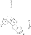
- a compound comprising a ligand L A of Formula I: is provided,
- a first device comprising a first organic light emitting device.
- the first organic light emitting device can include an anode, a cathode, and an organic layer, disposed between the anode and the cathode.
- the organic layer can include a compound comprising a ligand L A of Formula I.
- the first device can be one or more of a consumer product, an electronic component module, an organic light-emitting device, and a lighting panel.
- Formulations containing a compound comprising a ligand L A of Formula I are also provided.
- an OLED comprises at least one organic layer disposed between and electrically connected to an anode and a cathode.
- the anode injects holes and the cathode injects electrons into the organic layer(s).
- the injected holes and electrons each migrate toward the oppositely charged electrode.
- an "exciton” which is a localized electron-hole pair having an excited energy state, is formed.
- Light is emitted when the exciton relaxes via a photoemissive mechanism.
- the exciton may be localized on an excimer or an exciplex. Non-radiative mechanisms, such as thermal relaxation, may also occur, but are generally considered undesirable.
- the initial OLEDs used emissive molecules that emitted light from their singlet states ("fluorescence") as disclosed, for example, in U.S. Pat. No. 4,769,292 . Fluorescent emission generally occurs in a time frame of less than 10 nanoseconds.
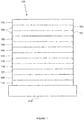
- FIG. 1 shows an organic light emitting device 100.
- Device 100 may include a substrate 110, an anode 115, a hole injection layer 120, a hole transport layer 125, an electron blocking layer 130, an emissive layer 135, a hole blocking layer 140, an electron transport layer 145, an electron injection layer 150, a protective layer 155, a cathode 160, and a barrier layer 170.
- Cathode 160 is a compound cathode having a first conductive layer 162 and a second conductive layer 164.
- Device 100 may be fabricated by depositing the layers described, in order. The properties and functions of these various layers, as well as example materials, are described in more detail in US 7,279,704 at cols. 6-10.
- a flexible and transparent substrate-anode combination is disclosed in U.S. Pat. No. 5,844,363 .
- An example of a p-doped hole transport layer is m-MTDATA doped with F 4 -TCNQ at a molar ratio of 50:1, as disclosed in U.S. Patent Application Publication No. 2003/0230980 .
- Examples of emissive and host materials are disclosed in U.S. Pat. No. 6,303,238 to Thompson et al.
- An example of an n-doped electron transport layer is BPhen doped with Li at a molar ratio of 1:1, as disclosed in U.S. Patent Application Publication No. 2003/0230980 .
- Pat. Nos. 5,703,436 and 5,707,745 disclose examples of cathodes including compound cathodes having a thin layer of metal such as Mg:Ag with an overlying transparent, electrically-conductive, sputter-deposited ITO layer.
- the theory and use of blocking layers is described in more detail in U.S. Pat. No. 6,097,147 and U.S. Patent Application Publication No. 2003/0230980 .
- Examples of injection layers are provided in U.S. Patent Application Publication No. 2004/0174116 .
- a description of protective layers may be found in U.S. Patent Application Publication No. 2004/0174116 .
- FIG. 2 shows an inverted OLED 200.
- the device includes a substrate 210, a cathode 215, an emissive layer 220, a hole transport layer 225, and an anode 230.
- Device 200 may be fabricated by depositing the layers described, in order. Because the most common OLED configuration has a cathode disposed over the anode, and device 200 has cathode 215 disposed under anode 230, device 200 may be referred to as an "inverted" OLED. Materials similar to those described with respect to device 100 may be used in the corresponding layers of device 200.
- FIG. 2 provides one example of how some layers may be omitted from the structure of device 100.
- FIGS. 1 and 2 The simple layered structure illustrated in FIGS. 1 and 2 is provided by way of non-limiting example, and it is understood that embodiments of the invention may be used in connection with a wide variety of other structures.
- the specific materials and structures described are exemplary in nature, and other materials and structures may be used.
- Functional OLEDs may be achieved by combining the various layers described in different ways, or layers may be omitted entirely, based on design, performance, and cost factors. Other layers not specifically described may also be included. Materials other than those specifically described may be used. Although many of the examples provided herein describe various layers as comprising a single material, it is understood that combinations of materials, such as a mixture of host and dopant, or more generally a mixture, may be used. Also, the layers may have various sublayers.
- hole transport layer 225 transports holes and injects holes into emissive layer 220, and may be described as a hole transport layer or a hole injection layer.
- an OLED may be described as having an "organic layer" disposed between a cathode and an anode. This organic layer may comprise a single layer, or may further comprise multiple layers of different organic materials as described, for example, with respect to FIGS. 1 and 2 .
- OLEDs comprised of polymeric materials (PLEDs) such as disclosed in U.S. Pat. No. 5,247,190 to Friend et al.
- PLEDs polymeric materials
- OLEDs having a single organic layer may be used.
- OLEDs may be stacked, for example as described in U.S. Pat. No. 5,707,745 to Forrest et al.
- the OLED structure may deviate from the simple layered structure illustrated in FIGS. 1 and 2 .
- the substrate may include an angled reflective surface to improve out-coupling, such as a mesa structure as described in U.S. Pat. No. 6,091,195 to Forrest et al. , and/or a pit structure as described in U.S. Pat. No. 5,834,893 to Bulovic et al.
- any of the layers of the various embodiments may be deposited by any suitable method.
- preferred methods include thermal evaporation, ink-jet, such as described in U.S. Pat. Nos. 6,013,982 and 6,087,196 , organic vapor phase deposition (OVPD), such as described in U.S. Pat. No. 6,337,102 to Forrest et al. , and deposition by organic vapor jet printing (OVJP), such as described in U.S. Pat. No. 7,431,968 .
- OVPD organic vapor phase deposition
- OJP organic vapor jet printing
- Other suitable deposition methods include spin coating and other solution based processes. Solution based processes are preferably carried out in nitrogen or an inert atmosphere.
- preferred methods include thermal evaporation.
- Preferred patterning methods include deposition through a mask, cold welding such as described in U.S. Pat. Nos. 6,294,398 and 6,468,819 , and patterning associated with some of the deposition methods such as ink-jet and OVJD. Other methods may also be used.
- the materials to be deposited may be modified to make them compatible with a particular deposition method.
- substituents such as alkyl and aryl groups, branched or unbranched, and preferably containing at least 3 carbons, may be used in small molecules to enhance their ability to undergo solution processing. Substituents having 20 carbons or more may be used, and 3-20 carbons is a preferred range. Materials with asymmetric structures may have better solution processibility than those having symmetric structures, because asymmetric materials may have a lower tendency to recrystallize. Dendrimer substituents may be used to enhance the ability of small molecules to undergo solution processing.
- Devices fabricated in accordance with embodiments of the present invention may further optionally comprise a barrier layer.
- a barrier layer One purpose of the barrier layer is to protect the electrodes and organic layers from damaging exposure to harmful species in the environment including moisture, vapor and/or gases, etc.
- the barrier layer may be deposited over, under or next to a substrate, an electrode, or over any other parts of a device including an edge.
- the barrier layer may comprise a single layer, or multiple layers.
- the barrier layer may be formed by various known chemical vapor deposition techniques and may include compositions having a single phase as well as compositions having multiple phases. Any suitable material or combination of materials may be used for the barrier layer.
- the barrier layer may incorporate an inorganic or an organic compound or both.
- the preferred barrier layer comprises a mixture of a polymeric material and a non-polymeric material as described in U.S. Pat. No. 7,968,146 , PCT Pat. Application Nos. PCT/US2007/023098 (published as WO 2008/057394 A1 ) and PCT/US2009/042829 (published as WO 2010/011390 A2 ).
- the aforesaid polymeric and non-polymeric materials comprising the barrier layer should be deposited under the same reaction conditions and/or at the same time.
- the weight ratio of polymeric to non-polymeric material may be in the range of 95:5 to 5:95.
- the polymeric material and the non-polymeric material may be created from the same precursor material.
- the mixture of a polymeric material and a non-polymeric material consists essentially of polymeric silicon and inorganic silicon.
- Devices fabricated in accordance with embodiments of the invention can be incorporated into a wide variety of electronic component modules (or units) that can be incorporated into a variety of electronic products or intermediate components. Examples of such electronic products or intermediate components include display screens, lighting devices such as discrete light source devices or lighting panels, etc. that can be utilized by the end-user product manufacturers. Such electronic component modules can optionally include the driving electronics and/or power source(s). Devices fabricated in accordance with embodiments of the invention can be incorporated into a wide variety of consumer products that have one or more of the electronic component modules (or units) incorporated therein. Such consumer products would include any kind of products that include one or more light source(s) and/or one or more of some type of visual displays.
- Some examples of such consumer products include flat panel displays, computer monitors, medical monitors, televisions, billboards, lights for interior or exterior illumination and/or signaling, heads-up displays, fully or partially transparent displays, flexible displays, laser printers, telephones, cell phones, tablets, phablets, personal digital assistants (PDAs), laptop computers, digital cameras, camcorders, viewfinders, micro-displays, 3-D displays, vehicles, a large area wall, theater or stadium screen, or a sign.
- PDAs personal digital assistants
- Various control mechanisms may be used to control devices fabricated in accordance with the present invention, including passive matrix and active matrix. Many of the devices are intended for use in a temperature range comfortable to humans, such as 18 degrees C to 30 degrees C, and more preferably at room temperature (20-25 degrees C), but could be used outside this temperature range, for example, from -40 degrees C to + 80 degrees C.
- the materials and structures described herein may have applications in devices other than OLEDs.
- other opto-electronic devices such as organic solar cells and organic photodetectors may employ the materials and structures.
- organic devices such as organic transistors, may employ the materials and structures.
- halo include fluorine, chlorine, bromine, and iodine.
- alkyl as used herein contemplates both straight and branched chain alkyl radicals.
- Preferred alkyl groups are those containing from one to fifteen carbon atoms and include methyl, ethyl, propyl, isopropyl, butyl, isobutyl, tert-butyl, and the like. Additionally, the alkyl group may be optionally substituted.
- cycloalkyl as used herein contemplates cyclic alkyl radicals.
- Preferred cycloalkyl groups are those containing 3 to 7 carbon atoms and include cyclopropyl, cyclopentyl, cyclohexyl, and the like. Additionally, the cycloalkyl group may be optionally substituted.
- alkenyl as used herein contemplates both straight and branched chain alkene radicals.
- Preferred alkenyl groups are those containing two to fifteen carbon atoms. Additionally, the alkenyl group may be optionally substituted.
- alkynyl as used herein contemplates both straight and branched chain alkyne radicals. Preferred alkynyl groups are those containing two to fifteen carbon atoms. Additionally, the alkynyl group may be optionally substituted.
- aralkyl or "arylalkyl” as used herein are used interchangeably and contemplate an alkyl group that has as a substituent an aromatic group. Additionally, the aralkyl group may be optionally substituted.
- heterocyclic group contemplates aromatic and non-aromatic cyclic radicals.
- Hetero-aromatic cyclic radicals also means heteroaryl.
- Preferred hetero-non-aromatic cyclic groups are those containing 3 or 7 ring atoms which includes at least one hetero atom, and includes cyclic amines such as morpholino, piperdino, pyrrolidino, and the like, and cyclic ethers, such as tetrahydrofuran, tetrahydropyran, and the like. Additionally, the heterocyclic group may be optionally substituted.
- aryl or "aromatic group” as used herein contemplate single-ring groups and polycyclic ring systems.
- the polycyclic rings may have two or more rings in which two carbons are common to two adjoining rings (the rings are "fused") wherein at least one of the rings is aromatic, e.g., the other rings can be cycloalkyls, cycloalkenyls, aryl, heterocycles, and/or heteroaryls. Additionally, the aryl group may be optionally substituted.
- heteroaryl as used herein contemplates single-ring hetero-aromatic groups that may include from one to three heteroatoms, for example, pyrrole, furan, thiophene, imidazole, oxazole, thiazole, triazole, pyrazole, pyridine, pyrazine and pyrimidine, and the like.
- heteroaryl also includes polycyclic hetero-aromatic systems having two or more rings in which two atoms are common to two adjoining rings (the rings are "fused") wherein at least one of the rings is a heteroaryl, e.g., the other rings can be cycloalkyls, cycloalkenyls, aryl, heterocycles, and/or heteroaryls. Additionally, the heteroaryl group may be optionally substituted.
- alkyl, cycloalkyl, alkenyl, alkynyl, aralkyl, heterocyclic group, aryl, and heteroaryl may be optionally substituted with one or more substituents selected from the group consisting of hydrogen, deuterium, halogen, alkyl, cycloalkyl, heteroalkyl, arylalkyl, alkoxy, aryloxy, amino, cyclic amino, silyl, alkenyl, cycloalkenyl, heteroalkenyl, alkynyl, aryl, heteroaryl, acyl, carbonyl, carboxylic acid, ether, ester, nitrile, isonitrile, sulfanyl, sulfinyl, sulfonyl, phosphino, and combinations thereof.
- substituted indicates that a substituent other than H is bonded to the relevant position, such as carbon.
- substituent other than H such as carbon.
- R 1 is mono-substituted
- one R 1 must be other than H.
- R 1 is di-substituted
- two of R 1 must be other than H.
- R 1 is hydrogen for all available positions.
- aza-dibenzofuran i.e. aza-dibenzofuran, aza-dibenzothiophene, etc.
- azatriphenylene encompasses both dibenzo[ f , h ]quinoxaline and dibenzo[ f,h ]quinoline.
- the compounds described herein are metal complexes containing an azadibenzofuranyl imidazole carbene ligand.
- the introduction of the azadibenzofuran moiety can lower the LUMO of the complex compared to dibenzofuran containing complexes, resulting in better device stability.
- the rigidity of the ligand containing the azadibenzofuran moiety makes the emission spectrum narrower, which is desirable for more saturated colors.
- a compound comprising a ligand L A of Formula I: is disclosed.
- the compound has the formula M(L A ) m (L B ) n of the structure:
- M is selected from the group consisting of Ir, Rh, Re, Ru, Os, Pt, Au, and Cu. In some embodiments, M is Ir.
- X 1 is O.
- M is coordinated to ring B through a M-C bond.
- only one of A 1 , A 2 , A 3 , A 4 , A 5 , A 6 , A 7 , and A 8 is nitrogen.
- each one of A 1 , A 2 , A 3 , and A 4 is carbon.
- each one of A 1 , A 2 , A 3 , and A 4 is carbon, and exactly one of A 5 , A 6 , A 7 , and A 8 is nitrogen.
- only two of A 1 , A 2 , A 3 , A 4 , A 5 , A 6 , A 7 , and A 8 are nitrogen.
- each one of A 1 , A 2 , A 3 , and A 4 is carbon, and exactly two of A 5 , A 6 , A 7 , and A 8 are nitrogen.
- R 2 forms a phenyl or pyridyl ring fused to ring A.
- Ring A is selected from the group consisting of:
- the ligand L A is where R 3 is selected from the group consisting of hydrogen, deuterium, halide, alkyl, cycloalkyl, heteroalkyl, arylalkyl, alkoxy, aryloxy, amino, silyl, alkenyl, cycloalkenyl, heteroalkenyl, alkynyl, aryl, heteroaryl, acyl, carbonyl, carboxylic acids, ester, nitrile, isonitrile, sulfanyl, sulfinyl, sulfonyl, phosphino, and combinations thereof.
- the compound is selected from the group consisting of and
- the compound is selected from the group consisting of and
- m is 1.
- R 1 is selected from the group consisting of hydrogen, deuterium, alkyl, cycloalkyl, and combinations thereof. In some embodiments, R 1 is selected from the group consisting of methyl, ethyl, isopropyl, isobutyl, cyclopentyl and partially or fully deuterated variations thereof.
- R 2 is selected from the group consisting of hydrogen, a phenyl ring fused to ring A, and a pyridyl ring fused to ring A.
- R 3 is alkyl or cycloalkyl. In some embodiments, R 3 is aryl or substituted aryl.
- R 3 is selected from the group consisting of: methyl, ethyl, propyl, 1-methylethyl, butyl, 1-methylpropyl, 2-methylpropyl, pentyl, 1-methylbutyl, 2-methylbutyl, 3-methylbutyl, 1,1-dimethylpropyl, 1,2-dimethylpropyl, 2,2-dimethylpropyl, cyclopentyl, and cyclohexyl, wherein each group is optionally partially or fully deuterated.
- R 5 is selected from the group consisting of alkyl, cycloalkyl, aryl and substituted aryl.
- R 7 is a 2,6-disubstituted aryl.
- R 7 is a 2,6-disubstituted phenyl, substituted with an alkyl selected from the group consisting of methyl, ethyl, isopropyl, isobutyl, and partially or fully deuterated variations thereof.
- R 7 comprises at least one chemical group selected from the group consisting of carbazole, dibenzothiophene, dibenzofuran, and fluorine.
- Y 5 , Y 6 , Y 7 , and Y 8 comprise carbon, only one of Y 1 , Y 2 , Y 3 , Y 4 is nitrogen. In some embodiments, Y 2 is nitrogen.
- R 8 is selected from the group consisting of hydrogen, deuterium, halide, alkyl, cycloalkyl, and combinations thereof. In some embodiments, R 8 is selected from the group consisting of methyl, ethyl, isopropyl, isobutyl, and partially or fully deuterated variations thereof. In some embodiments, adjacent R 8 substituents are joined together with Ring C to form dibenzofuran, azadibenzofuran, dibenzothiophene, or azadibenzothiophene.
- R 9 is selected from the group consisting of hydrogen, deuterium, alkyl, cycloalkyl, and combinations thereof. In some embodiments, R 9 is selected from the group consisting of methyl, ethyl, isopropyl, isobutyl, deuterated variations thereof, phenyl, alkyl substituted phenyl, pyridyl, alkyl substituted pyridyl, fused phenyl, and alkyl substituted fused phenyl.
- the ligand L A is: where: R 10 is selected from the group consisting of of hydrogen, deuterium, halide, alkyl, cycloalkyl, heteroalkyl, arylalkyl, alkoxy, aryloxy, amino, silyl, alkenyl, cycloalkenyl, heteroalkenyl, alkynyl, aryl, heteroaryl, acyl, carbonyl, carboxylic acids, ester, nitrile, isonitrile, sulfanyl, sulfinyl, sulfonyl, phosphino, and combinations thereof.
- ligand L A is N-(2-aminoethyl)-2-aminoethyl-N-(2-aminoethyl)-2-aminoethyl-N-(2-aminoethyl)-2-aminoethyl-N-(2-aminoethyl)-2-aminoethyl-N-(2-aminoethyl)-2-aminoethyl-N-(2-aminoethyl)-2-aminoethyl-N-(2-aminoethyl)-2-aminoethyl-N-(2-aminoethyl)-2-aminoethyl-N-(2-aminoethyl)-2-aminoethyl-N-(2-aminoethyl)-2-aminoethyl-N-(2-aminoethyl)-2-aminoethyl-N
- R 10 is selected from the group consisting of hydrogen, deuterium, alkyl, and combinations thereof. In some embodiments, R 10 is alkyl. In some embodiments, R 10 is cycloalkyl. In some embodiments, R 10 is selected from the group consisting of methyl, ethyl, propyl, 1-methylethyl, butyl, 1-methylpropyl, 2-methylpropyl, pentyl, 1-methylbutyl, 2-methylbutyl, 3-methylbutyl, 1,1-dimethylpropyl, 1,2-dimethylpropyl, 2,2-dimethylpropyl, cyclopentyl, cyclohexyl, partially or fully deuterated variants thereof, and combinations thereof.
- L A is selected from the group consisting of:
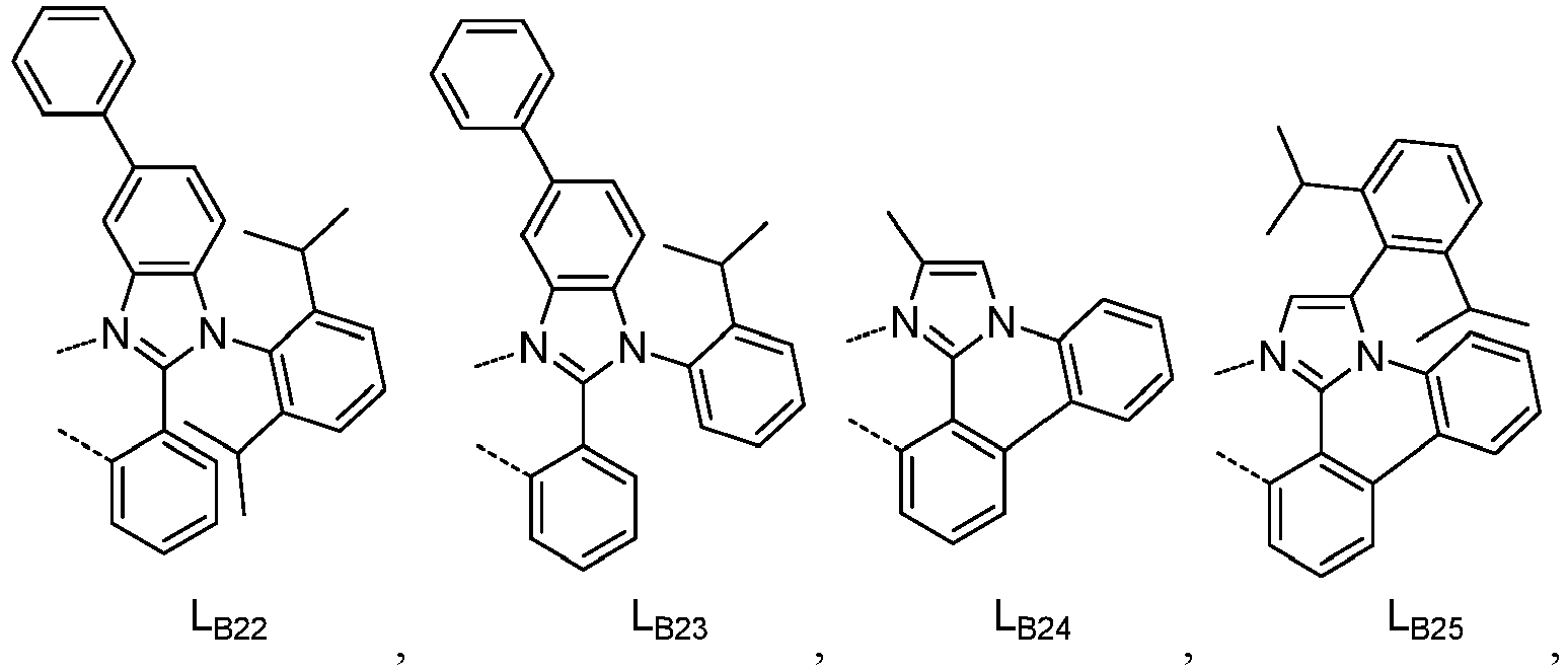
- L B is selected from the group consisting of:
- L A1 to L A80 have the definitions herein
- L B1 to L B76 have the definitions herein
- the compound can be an emissive dopant.
- the compound can produce emissions via phosphorescence, fluorescence, thermally activated delayed fluorescence, i.e., TADF (also referred to as E-type delayed fluorescence), triplet-triplet annihilation, or combinations of these processes.
- TADF thermally activated delayed fluorescence
- a first device includes a first organic light emitting device, that includes an anode, a cathode, and an organic layer disposed between the anode and the cathode.
- the organic layer can include a compound comprising a ligand L A of Formula I and its variants as described herein.
- the organic layer includes a host and a phosphorescent dopant.
- the first device can be one or more of a a consumer product, an electronic component module, an organic light-emitting device, and a lighting panel.
- the organic layer can be an emissive layer and the compound can be an emissive dopant in some embodiments, while the compound can be a non-emissive dopant in other embodiments.
- the organic layer can also include a host.
- the host can include a metal complex.
- n can range from 1 to 10; and Ar 1 and Ar 2 can be independently selected from the group consisting of benzene, biphenyl, naphthalene, triphenylene, carbazole, and heteroaromatic analogs thereof.
- the host can be a compound comprising at least one chemical group selected from the group consisting of triphenylene, carbazole, dibenzothiphene, dibenzofuran, dibenzoselenophene, azatriphenylene, azacarbazole, aza-dibenzothiophene, aza-dibenzofuran, and aza-dibenzoselenophene.
- the host can include a metal complex.
- the host can be a specific compound selected from the group consisting of: and combinations thereof.
- a formulation that comprises a compound comprising a ligand L A of Formula I, and its variations described herein, is described.
- the formulation can include one or more components selected from the group consisting of a solvent, a host, a hole injection material, hole transport material, and an electron transport layer material, disclosed herein.
- the materials described herein as useful for a particular layer in an organic light emitting device may be used in combination with a wide variety of other materials present in the device.
- emissive dopants disclosed herein may be used in conjunction with a wide variety of hosts, transport layers, blocking layers, injection layers, electrodes and other layers that may be present.
- the materials described or referred to below are non-limiting examples of materials that may be useful in combination with the compounds disclosed herein, and one of skill in the art can readily consult the literature to identify other materials that may be useful in combination.
- a hole injecting/transporting material to be used in the present invention is not particularly limited, and any compound may be used as long as the compound is typically used as a hole injecting/transporting material.
- the material include, but not limit to: a phthalocyanine or porphyrin derivative; an aromatic amine derivative; an indolocarbazole derivative; a polymer containing fluorohydrocarbon; a polymer with conductivity dopants; a conducting polymer, such as PEDOT/PSS; a self-assembly monomer derived from compounds such as phosphonic acid and silane derivatives; a metal oxide derivative, such as MoO x ; a p-type semiconducting organic compound, such as 1,4,5,8,9,12-Hexaazatriphenylenehexacarbonitrile; a metal complex, and a cross-linkable compound.
- aromatic amine derivatives used in HIL or HTL include, but not limit to the following general structures:
- Each of Ar 1 to Ar 9 is selected from the group consisting of aromatic hydrocarbon cyclic compounds such as benzene, biphenyl, triphenyl, triphenylene, naphthalene, anthracene, phenalene, phenanthrene, fluorene, pyrene, chrysene, perylene, and azulene; the group consisting of aromatic heterocyclic compounds such as dibenzothiophene, dibenzofuran, dibenzoselenophene, furan, thiophene, benzofuran, benzothiophene, benzoselenophene, carbazole, indolocarbazole, pyridylindole, pyrrolodipyridine, pyrazole, imidazole, triazole, oxazole, thiazole, oxadiazole, oxatriazole, dioxazole, thiadiazole, pyridine, pyridazine
- each Ar is further substituted by a substituent selected from the group consisting of hydrogen, deuterium, halide, alkyl, cycloalkyl, heteroalkyl, arylalkyl, alkoxy, aryloxy, amino, silyl, alkenyl, cycloalkenyl, heteroalkenyl, alkynyl, aryl, heteroaryl, acyl, carbonyl, carboxylic acids, ester, nitrile, isonitrile, sulfanyl, sulfinyl, sulfonyl, phosphino, and combinations thereof.
- a substituent selected from the group consisting of hydrogen, deuterium, halide, alkyl, cycloalkyl, heteroalkyl, arylalkyl, alkoxy, aryloxy, amino, silyl, alkenyl, cycloalkenyl, heteroalkenyl, alkynyl, aryl, heteroaryl, acy
- Ar 1 to Ar 9 is independently selected from the group consisting of: wherein k is an integer from 1 to 20; X 101 to X 108 is C (including CH) or N; Z 101 is NAr 1 , O, or S; Ar 1 has the same group defined above.
- metal complexes used in HIL or HTL include, but not limit to the following general formula: wherein Met is a metal, which can have an atomic weight greater than 40; (Y 101 -Y 102 ) is a bidentate ligand, Y 101 and Y 102 are independently selected from C, N, O, P, and S; L 101 is an ancillary ligand; k' is an integer value from 1 to the maximum number of ligands that may be attached to the metal; and k'+k" is the maximum number of ligands that may be attached to the metal.
- (Y 101 -Y 102 ) is a 2-phenylpyridine derivative. In another aspect, (Y 101 -Y 102 ) is a carbene ligand. In another aspect, Met is selected from Ir, Pt, Os, and Zn. In a further aspect, the metal complex has a smallest oxidation potential in solution vs. Fc + /Fc couple less than about 0.6 V.
- the light emitting layer of the organic EL device of the present invention preferably contains at least a metal complex as light emitting material, and may contain a host material using the metal complex as a dopant material.
- the host material are not particularly limited, and any metal complexes or organic compounds may be used as long as the triplet energy of the host is larger than that of the dopant. While the Table below categorizes host materials as preferred for devices that emit various colors, any host material may be used with any dopant so long as the triplet criteria is satisfied.
- Examples of metal complexes used as host are preferred to have the following general formula: wherein Met is a metal; (Y 103 -Y 104 ) is a bidentate ligand, Y 103 and Y 104 are independently selected from C, N, O, P, and S; L 101 is an another ligand; k' is an integer value from 1 to the maximum number of ligands that may be attached to the metal; and k'+k" is the maximum number of ligands that may be attached to the metal.
- the metal complexes are: wherein (O-N) is a bidentate ligand, having metal coordinated to atoms O and N.
- Met is selected from Ir and Pt.
- (Y 103 -Y 104 ) is a carbene ligand.
- organic compounds used as host are selected from the group consisting of aromatic hydrocarbon cyclic compounds such as benzene, biphenyl, triphenyl, triphenylene, naphthalene, anthracene, phenalene, phenanthrene, fluorene, pyrene, chrysene, perylene, and azulene; the group consisting of aromatic heterocyclic compounds such as dibenzothiophene, dibenzofuran, dibenzoselenophene, furan, thiophene, benzofuran, benzothiophene, benzoselenophene, carbazole, indolocarbazole, pyridylindole, pyrrolodipyridine, pyrazole, imidazole, triazole, oxazole, thiazole, oxadiazole, oxatriazole, dioxazole, thiadiazole, pyridine, pyridazine,
- each group is further substituted by a substituent selected from the group consisting of hydrogen, deuterium, halide, alkyl, cycloalkyl, heteroalkyl, arylalkyl, alkoxy, aryloxy, amino, silyl, alkenyl, cycloalkenyl, heteroalkenyl, alkynyl, aryl, heteroaryl, acyl, carbonyl, carboxylic acids, ester, nitrile, isonitrile, sulfanyl, sulfinyl, sulfonyl, phosphino, and combinations thereof.
- a substituent selected from the group consisting of hydrogen, deuterium, halide, alkyl, cycloalkyl, heteroalkyl, arylalkyl, alkoxy, aryloxy, amino, silyl, alkenyl, cycloalkenyl, heteroalkenyl, alkynyl, aryl, heteroaryl, acy
- the host compound contains at least one of the following groups in the molecule: wherein R 101 to R 107 is independently selected from the group consisting of hydrogen, deuterium, halide, alkyl, cycloalkyl, heteroalkyl, arylalkyl, alkoxy, aryloxy, amino, silyl, alkenyl, cycloalkenyl, heteroalkenyl, alkynyl, aryl, heteroaryl, acyl, carbonyl, carboxylic acids, ester, nitrile, isonitrile, sulfanyl, sulfinyl, sulfonyl, phosphino, and combinations thereof, when it is aryl or heteroaryl, it has the similar definition as Ar's mentioned above.
- k is an integer from 0 to 20 or 1 to 20;
- k'" is an integer from 0 to 20.
- X 101 to X 108 is selected from C (including CH) or N.
- Z 101 and Z 102 is selected from NR 101 , O, or S.
- a hole blocking layer may be used to reduce the number of holes and/or excitons that leave the emissive layer.
- the presence of such a blocking layer in a device may result in substantially higher efficiencies as compared to a similar device lacking a blocking layer.
- a blocking layer may be used to confine emission to a desired region of an OLED.
- compound used in HBL contains the same molecule or the same functional groups used as host described above.
- compound used in HBL contains at least one of the following groups in the molecule: wherein k is an integer from 1 to 20; L 101 is an another ligand, k' is an integer from 1 to 3.
- Electron transport layer may include a material capable of transporting electrons. Electron transport layer may be intrinsic (undoped), or doped. Doping may be used to enhance conductivity. Examples of the ETL material are not particularly limited, and any metal complexes or organic compounds may be used as long as they are typically used to transport electrons.
- compound used in ETL contains at least one of the following groups in the molecule: wherein R 101 is selected from the group consisting of hydrogen, deuterium, halide, alkyl, cycloalkyl, heteroalkyl, arylalkyl, alkoxy, aryloxy, amino, silyl, alkenyl, cycloalkenyl, heteroalkenyl, alkynyl, aryl, heteroaryl, acyl, carbonyl, carboxylic acids, ester, nitrile, isonitrile, sulfanyl, sulfinyl, sulfonyl, phosphino, and combinations thereof, when it is aryl or heteroaryl, it has the similar definition as Ar's mentioned above.
- Ar 1 to Ar 3 has the similar definition as Ar's mentioned above.
- k is an integer from 1 to 20.
- X 101 to X 108 is selected from C (including CH) or N.
- the metal complexes used in ETL contains, but not limit to the following general formula: wherein (O-N) or (N-N) is a bidentate ligand, having metal coordinated to atoms O, N or N, N; L 101 is another ligand; k' is an integer value from 1 to the maximum number of ligands that may be attached to the metal.
- the hydrogen atoms can be partially or fully deuterated.
- any specifically listed substituent such as, without limitation, methyl, phenyl, pyridyl, etc. encompasses undeuterated, partially deuterated, and fully deuterated versions thereof.
- classes of substituents such as, without limitation, alkyl, aryl, cycloalkyl, heteroaryl, etc. also encompass undeuterated, partially deuterated, and fully deuterated versions thereof.
- hole injection materials In addition to and/or in combination with the materials disclosed herein, many hole injection materials, hole transporting materials, host materials, dopant materials, exciton/hole blocking layer materials, electron transporting and electron injecting materials may be used in an OLED.
- Non-limiting examples of the materials that may be used in an OLED in combination with materials disclosed herein are listed in Table A below. Table A lists non-limiting classes of materials, non-limiting examples of compounds for each class, and references that disclose the materials. TABLE A MATERIAL EXAMPLES OF MATERIAL PUBLICATIONS Hole injection materials Phthalocyanine and porphyrin compounds Appl. Phys. Lett. 69, 2160 (1996 ) Starburst triarylamines J. Lumin.
- Compound 963 were compared against Comparative Compound 1.
- a 5% doped PMMA film of Comparative Compound 1 exhibited a 56% PLQY
- a 5% doped PMMA film of Compound 963 exhibited a PLQY of 86%, which is much higher than that of the comparative compound. It is advantageous to have higher PLQY as an emitter in the OLED device.
Landscapes
- Chemical & Material Sciences (AREA)
- Organic Chemistry (AREA)
- Engineering & Computer Science (AREA)
- Materials Engineering (AREA)
- Crystallography & Structural Chemistry (AREA)
- Inorganic Chemistry (AREA)
- Electroluminescent Light Sources (AREA)
Claims (13)
- Eine Verbindung umfassend einen Liganden LA gemäß Formel I:
 wobei jedes A1, A2, A3, A4, A5, A6, A7 und A8 unabhängig Kohlenstoff oder Stickstoff ist;wobei mindestens eines von A1, A2, A3, A4, A5, A6, A7 und A8 Stickstoff ist;wobei X1 ausgewählt ist aus der Gruppe bestehend aus O, S und Se;wobei Ring A mittels einer N-C Bindung an Ring B gebunden ist;wobei Ring A ausgewählt ist aus der Gruppe bestehend aus:
 wobei die Wellenlinie die Bindung an Ring B anzeigt;wobei R3 ausgewählt ist aus der Gruppe bestehend aus Wasserstoff, Deuterium, Halogen, Alkyl, Cycloalkyl, Heteroalkyl, Arylalkyl, Alkoxy, Aryloxy, Amino, Silyl, ,Alkenyl, Cycloalkenyl, Heteroalkenyl, Alkinyl, Aryl, Heteroaryl, Acyl, Carbonyl, Carbonsäuren, Ester, Nitril, Isonitril, Sulfanyl,Sulfinyl, Sulfonyl, Phosphino, und deren Kombinationen;wobei R1 für mono-, di-, tri-, oder tetra-Substitutionen, oder keine Substitution steht;wobei beliebige benachbarte Substitutionen aus R1 gegebenenfalls miteinander verbunden sind um einen Ring zu bilden;wobei R1 ausgewählt ist aus der Gruppe bestehend aus Wasserstoff, Deuterium, Halogen, Alkyl, Cycloalkyl, Heteroalkyl, Arylalkyl, Alkoxy, Aryloxy, Amino, Silyl, ,Alkenyl, Cycloalkenyl, Heteroalkenyl, Alkinyl, Aryl, Heteroaryl, Acyl, Carbonyl, Carbonsäuren, Ester, Nitril, Isonitril, Sulfanyl,Sulfinyl, Sulfonyl, Phosphino, und deren Kombinationen;wobei der Ligand LA an ein Metall M koordiniert ist;wobei M an Ring A über eine Metallcarbenbindung koordiniert ist; undwobei der Ligand LA gegebenenfalls mit anderen Liganden verknüpft ist um einen tridentaten, tetradentaten, pentadentaten oder hexadentaten Liganden zu umfassen.
 - Die Verbindung nach Anspruch 1, wobei die Verbindung die Formel M(LA)m(LB), aufweist, mit folgender Struktur:
 wobei LB ein von LA verschiedener Ligand ist;wobei m eine ganze Zahl von 1 zur maximalen Zahl der Liganden, die an das Metall M koordiniert sein können; undm+n die maximale Zahl an Liganden ist, die an das Metall M koordiniert sein kann.
 - Die Verbindung nach Anspruch 1, wobei M ausgewählt ist aus der Gruppe bestehend aus Ir, Rh, Re, Ru, Os, Pt, Au, und Cu.
- Die Verbindung nach einem der Ansprüche bis 3, wobei M an Ring B über eine M-C Bindung koordiniert ist.
- Die Verbindung nach einem der Ansprüche bis 4, wobei nur einer von A1, A2, A3, A4, A5, A6, A7, and A8 Stickstoff ist, und/oder jeder von A1, A2, A3 und A4 Kohlenstoff ist.
- Die Verbindung nach Anspruch 1, wobei der Ligand LA ist:

- Die Verbindung nach Anspruch 6, wobei der Ligand LA ist:

- Die Verbindung nach Anspruch 6 oder 7, wobei R10 ausgewählt ist aus der Gruppe bestehend aus Wasserstoff, Deuterium, Alkyl, Cycloalkyl, teilweise oder vollständig deuterierte Varianten davon, insbesondere Methyl, Ethyl, Propyl, 1-Methylethyl, Butyl, 1-Methylpropyl, 2-Methylpropyl, Pentyl, 1-Methylbutyl, 2-Methylbutyl, 3-Methylbutyl, 1,1-Dimethylpropyl, 1,2-Dimethylpropyl, 2,2-Dimethylpropyl, Cyclopentyl, Cyclohexyl, teilweise oder vollständig deuterierte Varianten davon, und Kombinationen davon.
- Die Verbindung nach Anspruch 2, wobei LB ausgewählt ist aus der Gruppe bestehend aus:




- Eine erste Vorrichtung umfassend eine erste organische Licht emittierende Vorrichtung, wobei die erste organische Licht emittierende Vorrichtung umfasst:eine Anode;eine Kathode; undeine organische Schicht, angeordnet zwischen der Anode und der Kathode, umfassend eine Verbindung wie in einem der vorhergehenden Ansprüche definiert.
- Die erste Vorrichtung nach Anspruch 10, wobei die erste Vorrichtung ausgewählt ist aus der Gruppe bestehend aus einem Konsumentenprodukt, einem elektronischen Komponentenmodul, einer organischen Licht emittierenden Vorrichtung, und einer Lichtleiste.
- Die erste Vorrichtung nach Anspruch 10 oder 11, wobei die organische Schicht eine emittierende Schicht und die Verbindung ein emittierender Dotierstoff oder ein nicht emittierender Dotierstoff ist.
- Eine Formulierung umfassend eine Verbindung wie in einem der Ansprüche bis 9 definiert.
Applications Claiming Priority (5)
| Application Number | Priority Date | Filing Date | Title |
|---|---|---|---|
| US201361904530P | 2013-11-15 | 2013-11-15 | |
| US201361907450P | 2013-11-22 | 2013-11-22 | |
| US14/521,257 US9905784B2 (en) | 2013-11-15 | 2014-10-22 | Organic electroluminescent materials and devices |
| US14/521,281 US10033000B2 (en) | 2013-11-15 | 2014-10-22 | Organic electroluminescent materials and devices |
| EP14003750.8A EP2874192B1 (de) | 2013-11-15 | 2014-11-06 | Organische elektrolumineszente Materialien und Vorrichtungen |
Related Parent Applications (1)
| Application Number | Title | Priority Date | Filing Date |
|---|---|---|---|
| EP14003750.8A Division EP2874192B1 (de) | 2013-11-15 | 2014-11-06 | Organische elektrolumineszente Materialien und Vorrichtungen |
Publications (2)
| Publication Number | Publication Date |
|---|---|
| EP3220441A1 EP3220441A1 (de) | 2017-09-20 |
| EP3220441B1 true EP3220441B1 (de) | 2020-04-22 |
Family
ID=51867985
Family Applications (4)
| Application Number | Title | Priority Date | Filing Date |
|---|---|---|---|
| EP17168434.3A Withdrawn EP3220440A1 (de) | 2013-11-15 | 2014-11-05 | Organische elektrolumineszente materialien und vorrichtungen |
| EP14003725.0A Active EP2874195B1 (de) | 2013-11-15 | 2014-11-05 | Organische elektrolumineszente Materialien und Vorrichtungen |
| EP17169173.6A Active EP3220441B1 (de) | 2013-11-15 | 2014-11-06 | Organische elektrolumineszente materialien und vorrichtungen |
| EP14003750.8A Active EP2874192B1 (de) | 2013-11-15 | 2014-11-06 | Organische elektrolumineszente Materialien und Vorrichtungen |
Family Applications Before (2)
| Application Number | Title | Priority Date | Filing Date |
|---|---|---|---|
| EP17168434.3A Withdrawn EP3220440A1 (de) | 2013-11-15 | 2014-11-05 | Organische elektrolumineszente materialien und vorrichtungen |
| EP14003725.0A Active EP2874195B1 (de) | 2013-11-15 | 2014-11-05 | Organische elektrolumineszente Materialien und Vorrichtungen |
Family Applications After (1)
| Application Number | Title | Priority Date | Filing Date |
|---|---|---|---|
| EP14003750.8A Active EP2874192B1 (de) | 2013-11-15 | 2014-11-06 | Organische elektrolumineszente Materialien und Vorrichtungen |
Country Status (1)
| Country | Link |
|---|---|
| EP (4) | EP3220440A1 (de) |
Families Citing this family (4)
| Publication number | Priority date | Publication date | Assignee | Title |
|---|---|---|---|---|
| CN117447526A (zh) * | 2018-09-15 | 2024-01-26 | 北京夏禾科技有限公司 | 含有氟取代的金属配合物 |
| CN110981895B (zh) * | 2018-12-17 | 2023-08-25 | 广州华睿光电材料有限公司 | 过渡金属配合物、聚合物、混合物、组合物及有机电子器件 |
| KR102687414B1 (ko) * | 2021-07-29 | 2024-07-22 | 엘지디스플레이 주식회사 | 유기금속 화합물 및 이를 포함하는 유기발광소자 |
| WO2023142983A1 (zh) * | 2022-01-27 | 2023-08-03 | 浙江光昊光电科技有限公司 | 一种氮杂卡宾碳自由基分子,包含其的混合物和组合物,及其在有机电子器件中的应用 |
Family Cites Families (23)
| Publication number | Priority date | Publication date | Assignee | Title |
|---|---|---|---|---|
| US4769292A (en) | 1987-03-02 | 1988-09-06 | Eastman Kodak Company | Electroluminescent device with modified thin film luminescent zone |
| GB8909011D0 (en) | 1989-04-20 | 1989-06-07 | Friend Richard H | Electroluminescent devices |
| US5703436A (en) | 1994-12-13 | 1997-12-30 | The Trustees Of Princeton University | Transparent contacts for organic devices |
| US5707745A (en) | 1994-12-13 | 1998-01-13 | The Trustees Of Princeton University | Multicolor organic light emitting devices |
| US5844363A (en) | 1997-01-23 | 1998-12-01 | The Trustees Of Princeton Univ. | Vacuum deposited, non-polymeric flexible organic light emitting devices |
| US5834893A (en) | 1996-12-23 | 1998-11-10 | The Trustees Of Princeton University | High efficiency organic light emitting devices with light directing structures |
| US6013982A (en) | 1996-12-23 | 2000-01-11 | The Trustees Of Princeton University | Multicolor display devices |
| US6091195A (en) | 1997-02-03 | 2000-07-18 | The Trustees Of Princeton University | Displays having mesa pixel configuration |
| US6303238B1 (en) | 1997-12-01 | 2001-10-16 | The Trustees Of Princeton University | OLEDs doped with phosphorescent compounds |
| US6337102B1 (en) | 1997-11-17 | 2002-01-08 | The Trustees Of Princeton University | Low pressure vapor phase deposition of organic thin films |
| US6087196A (en) | 1998-01-30 | 2000-07-11 | The Trustees Of Princeton University | Fabrication of organic semiconductor devices using ink jet printing |
| US6097147A (en) | 1998-09-14 | 2000-08-01 | The Trustees Of Princeton University | Structure for high efficiency electroluminescent device |
| US6294398B1 (en) | 1999-11-23 | 2001-09-25 | The Trustees Of Princeton University | Method for patterning devices |
| US7071615B2 (en) | 2001-08-20 | 2006-07-04 | Universal Display Corporation | Transparent electrodes |
| US7431968B1 (en) | 2001-09-04 | 2008-10-07 | The Trustees Of Princeton University | Process and apparatus for organic vapor jet deposition |
| US20030230980A1 (en) | 2002-06-18 | 2003-12-18 | Forrest Stephen R | Very low voltage, high efficiency phosphorescent oled in a p-i-n structure |
| US7279704B2 (en) | 2004-05-18 | 2007-10-09 | The University Of Southern California | Complexes with tridentate ligands |
| US7534505B2 (en) * | 2004-05-18 | 2009-05-19 | The University Of Southern California | Organometallic compounds for use in electroluminescent devices |
| US7491823B2 (en) * | 2004-05-18 | 2009-02-17 | The University Of Southern California | Luminescent compounds with carbene ligands |
| DE102004057072A1 (de) * | 2004-11-25 | 2006-06-01 | Basf Ag | Verwendung von Übergangsmetall-Carbenkomplexen in organischen Licht-emittierenden Dioden (OLEDs) |
| US7968146B2 (en) | 2006-11-01 | 2011-06-28 | The Trustees Of Princeton University | Hybrid layers for use in coatings on electronic devices or other articles |
| KR101933734B1 (ko) * | 2011-06-08 | 2018-12-28 | 유니버셜 디스플레이 코포레이션 | 헤테로렙틱 이리듐 카르벤 착물 및 이를 사용한 발광 디바이스 |
| US8692241B1 (en) * | 2012-11-08 | 2014-04-08 | Universal Display Corporation | Transition metal complexes containing triazole and tetrazole carbene ligands |
-
2014
- 2014-11-05 EP EP17168434.3A patent/EP3220440A1/de not_active Withdrawn
- 2014-11-05 EP EP14003725.0A patent/EP2874195B1/de active Active
- 2014-11-06 EP EP17169173.6A patent/EP3220441B1/de active Active
- 2014-11-06 EP EP14003750.8A patent/EP2874192B1/de active Active
Non-Patent Citations (1)
| Title |
|---|
| None * |
Also Published As
| Publication number | Publication date |
|---|---|
| EP3220441A1 (de) | 2017-09-20 |
| EP2874195A3 (de) | 2015-07-08 |
| EP2874195B1 (de) | 2017-05-03 |
| EP2874192A3 (de) | 2015-07-08 |
| EP3220440A1 (de) | 2017-09-20 |
| EP2874195A2 (de) | 2015-05-20 |
| EP2874192B1 (de) | 2017-05-10 |
| EP2874192A2 (de) | 2015-05-20 |
Similar Documents
| Publication | Publication Date | Title |
|---|---|---|
| JP7631417B2 (ja) | 有機エレクトロルミネセンス材料及びデバイス | |
| KR102445067B1 (ko) | 유기 전계발광 재료 및 디바이스 | |
| KR102702213B1 (ko) | 유기 전계발광 물질 및 디바이스 | |
| EP2982729B1 (de) | Organische elektrolumineszente materialien und vorrichtungen | |
| EP2891659B1 (de) | Organische elektrolumineszente Materialien und Vorrichtungen | |
| EP2927234B1 (de) | Organische elektrolumineszente materialien und vorrichtungen | |
| EP2933259B1 (de) | Organische elektrolumineszente materialien und vorrichtungen | |
| EP3007244B1 (de) | Organische elektrolumineszente materialien und vorrichtungen | |
| EP2711999B1 (de) | Elektrolumineszenzelement | |
| US9847498B2 (en) | Organic electroluminescent materials and devices | |
| EP3473634A1 (de) | Heteroleptische iridium-carben-komplexe und lichtemittierende vorrichtung zur verwendung davon | |
| EP3447053B1 (de) | Organische elektrolumineszente materialien und vorrichtungen | |
| EP3001480B1 (de) | Organische elektrolumineszente materialien und vorrichtungen | |
| EP3061763B1 (de) | Organische elektrolumineszente materialien und vorrichtungen | |
| EP2711408B1 (de) | Organische Verbindungen mit BN-Heterozyklen | |
| EP2769982B1 (de) | Deuterierte heteroleptische Iridium-Komplexe als phosphoreszierendes Material in OLEDS | |
| EP3220441B1 (de) | Organische elektrolumineszente materialien und vorrichtungen | |
| EP2963038B1 (de) | Organische elektrolumineszente materialien und vorrichtungen |
Legal Events
| Date | Code | Title | Description |
|---|---|---|---|
| PUAI | Public reference made under article 153(3) epc to a published international application that has entered the european phase |
Free format text: ORIGINAL CODE: 0009012 |
|
| STAA | Information on the status of an ep patent application or granted ep patent |
Free format text: STATUS: REQUEST FOR EXAMINATION WAS MADE |
|
| 17P | Request for examination filed |
Effective date: 20170503 |
|
| AC | Divisional application: reference to earlier application |
Ref document number: 2874192 Country of ref document: EP Kind code of ref document: P |
|
| AK | Designated contracting states |
Kind code of ref document: A1 Designated state(s): AL AT BE BG CH CY CZ DE DK EE ES FI FR GB GR HR HU IE IS IT LI LT LU LV MC MK MT NL NO PL PT RO RS SE SI SK SM TR |
|
| STAA | Information on the status of an ep patent application or granted ep patent |
Free format text: STATUS: EXAMINATION IS IN PROGRESS |
|
| 17Q | First examination report despatched |
Effective date: 20190903 |
|
| GRAP | Despatch of communication of intention to grant a patent |
Free format text: ORIGINAL CODE: EPIDOSNIGR1 |
|
| STAA | Information on the status of an ep patent application or granted ep patent |
Free format text: STATUS: GRANT OF PATENT IS INTENDED |
|
| INTG | Intention to grant announced |
Effective date: 20191220 |
|
| RAP1 | Party data changed (applicant data changed or rights of an application transferred) |
Owner name: UNIVERSAL DISPLAY CORPORATION |
|
| GRAS | Grant fee paid |
Free format text: ORIGINAL CODE: EPIDOSNIGR3 |
|
| GRAA | (expected) grant |
Free format text: ORIGINAL CODE: 0009210 |
|
| STAA | Information on the status of an ep patent application or granted ep patent |
Free format text: STATUS: THE PATENT HAS BEEN GRANTED |
|
| AC | Divisional application: reference to earlier application |
Ref document number: 2874192 Country of ref document: EP Kind code of ref document: P |
|
| AK | Designated contracting states |
Kind code of ref document: B1 Designated state(s): AL AT BE BG CH CY CZ DE DK EE ES FI FR GB GR HR HU IE IS IT LI LT LU LV MC MK MT NL NO PL PT RO RS SE SI SK SM TR |
|
| REG | Reference to a national code |
Ref country code: CH Ref legal event code: EP |
|
| REG | Reference to a national code |
Ref country code: DE Ref legal event code: R096 Ref document number: 602014064359 Country of ref document: DE |
|
| REG | Reference to a national code |
Ref country code: IE Ref legal event code: FG4D |
|
| REG | Reference to a national code |
Ref country code: AT Ref legal event code: REF Ref document number: 1261314 Country of ref document: AT Kind code of ref document: T Effective date: 20200515 |
|
| REG | Reference to a national code |
Ref country code: LT Ref legal event code: MG4D |
|
| REG | Reference to a national code |
Ref country code: NL Ref legal event code: MP Effective date: 20200422 |
|
| PG25 | Lapsed in a contracting state [announced via postgrant information from national office to epo] |
Ref country code: NO Free format text: LAPSE BECAUSE OF FAILURE TO SUBMIT A TRANSLATION OF THE DESCRIPTION OR TO PAY THE FEE WITHIN THE PRESCRIBED TIME-LIMIT Effective date: 20200722 Ref country code: IS Free format text: LAPSE BECAUSE OF FAILURE TO SUBMIT A TRANSLATION OF THE DESCRIPTION OR TO PAY THE FEE WITHIN THE PRESCRIBED TIME-LIMIT Effective date: 20200822 Ref country code: GR Free format text: LAPSE BECAUSE OF FAILURE TO SUBMIT A TRANSLATION OF THE DESCRIPTION OR TO PAY THE FEE WITHIN THE PRESCRIBED TIME-LIMIT Effective date: 20200723 Ref country code: FI Free format text: LAPSE BECAUSE OF FAILURE TO SUBMIT A TRANSLATION OF THE DESCRIPTION OR TO PAY THE FEE WITHIN THE PRESCRIBED TIME-LIMIT Effective date: 20200422 Ref country code: SE Free format text: LAPSE BECAUSE OF FAILURE TO SUBMIT A TRANSLATION OF THE DESCRIPTION OR TO PAY THE FEE WITHIN THE PRESCRIBED TIME-LIMIT Effective date: 20200422 Ref country code: LT Free format text: LAPSE BECAUSE OF FAILURE TO SUBMIT A TRANSLATION OF THE DESCRIPTION OR TO PAY THE FEE WITHIN THE PRESCRIBED TIME-LIMIT Effective date: 20200422 Ref country code: PT Free format text: LAPSE BECAUSE OF FAILURE TO SUBMIT A TRANSLATION OF THE DESCRIPTION OR TO PAY THE FEE WITHIN THE PRESCRIBED TIME-LIMIT Effective date: 20200824 Ref country code: NL Free format text: LAPSE BECAUSE OF FAILURE TO SUBMIT A TRANSLATION OF THE DESCRIPTION OR TO PAY THE FEE WITHIN THE PRESCRIBED TIME-LIMIT Effective date: 20200422 |
|
| REG | Reference to a national code |
Ref country code: AT Ref legal event code: MK05 Ref document number: 1261314 Country of ref document: AT Kind code of ref document: T Effective date: 20200422 |
|
| PG25 | Lapsed in a contracting state [announced via postgrant information from national office to epo] |
Ref country code: BG Free format text: LAPSE BECAUSE OF FAILURE TO SUBMIT A TRANSLATION OF THE DESCRIPTION OR TO PAY THE FEE WITHIN THE PRESCRIBED TIME-LIMIT Effective date: 20200722 Ref country code: HR Free format text: LAPSE BECAUSE OF FAILURE TO SUBMIT A TRANSLATION OF THE DESCRIPTION OR TO PAY THE FEE WITHIN THE PRESCRIBED TIME-LIMIT Effective date: 20200422 Ref country code: RS Free format text: LAPSE BECAUSE OF FAILURE TO SUBMIT A TRANSLATION OF THE DESCRIPTION OR TO PAY THE FEE WITHIN THE PRESCRIBED TIME-LIMIT Effective date: 20200422 Ref country code: LV Free format text: LAPSE BECAUSE OF FAILURE TO SUBMIT A TRANSLATION OF THE DESCRIPTION OR TO PAY THE FEE WITHIN THE PRESCRIBED TIME-LIMIT Effective date: 20200422 |
|
| PG25 | Lapsed in a contracting state [announced via postgrant information from national office to epo] |
Ref country code: AL Free format text: LAPSE BECAUSE OF FAILURE TO SUBMIT A TRANSLATION OF THE DESCRIPTION OR TO PAY THE FEE WITHIN THE PRESCRIBED TIME-LIMIT Effective date: 20200422 |
|
| REG | Reference to a national code |
Ref country code: DE Ref legal event code: R097 Ref document number: 602014064359 Country of ref document: DE |
|
| PG25 | Lapsed in a contracting state [announced via postgrant information from national office to epo] |
Ref country code: AT Free format text: LAPSE BECAUSE OF FAILURE TO SUBMIT A TRANSLATION OF THE DESCRIPTION OR TO PAY THE FEE WITHIN THE PRESCRIBED TIME-LIMIT Effective date: 20200422 Ref country code: EE Free format text: LAPSE BECAUSE OF FAILURE TO SUBMIT A TRANSLATION OF THE DESCRIPTION OR TO PAY THE FEE WITHIN THE PRESCRIBED TIME-LIMIT Effective date: 20200422 Ref country code: SM Free format text: LAPSE BECAUSE OF FAILURE TO SUBMIT A TRANSLATION OF THE DESCRIPTION OR TO PAY THE FEE WITHIN THE PRESCRIBED TIME-LIMIT Effective date: 20200422 Ref country code: DK Free format text: LAPSE BECAUSE OF FAILURE TO SUBMIT A TRANSLATION OF THE DESCRIPTION OR TO PAY THE FEE WITHIN THE PRESCRIBED TIME-LIMIT Effective date: 20200422 Ref country code: IT Free format text: LAPSE BECAUSE OF FAILURE TO SUBMIT A TRANSLATION OF THE DESCRIPTION OR TO PAY THE FEE WITHIN THE PRESCRIBED TIME-LIMIT Effective date: 20200422 Ref country code: RO Free format text: LAPSE BECAUSE OF FAILURE TO SUBMIT A TRANSLATION OF THE DESCRIPTION OR TO PAY THE FEE WITHIN THE PRESCRIBED TIME-LIMIT Effective date: 20200422 Ref country code: CZ Free format text: LAPSE BECAUSE OF FAILURE TO SUBMIT A TRANSLATION OF THE DESCRIPTION OR TO PAY THE FEE WITHIN THE PRESCRIBED TIME-LIMIT Effective date: 20200422 Ref country code: ES Free format text: LAPSE BECAUSE OF FAILURE TO SUBMIT A TRANSLATION OF THE DESCRIPTION OR TO PAY THE FEE WITHIN THE PRESCRIBED TIME-LIMIT Effective date: 20200422 |
|
| PG25 | Lapsed in a contracting state [announced via postgrant information from national office to epo] |
Ref country code: PL Free format text: LAPSE BECAUSE OF FAILURE TO SUBMIT A TRANSLATION OF THE DESCRIPTION OR TO PAY THE FEE WITHIN THE PRESCRIBED TIME-LIMIT Effective date: 20200422 Ref country code: SK Free format text: LAPSE BECAUSE OF FAILURE TO SUBMIT A TRANSLATION OF THE DESCRIPTION OR TO PAY THE FEE WITHIN THE PRESCRIBED TIME-LIMIT Effective date: 20200422 |
|
| PLBE | No opposition filed within time limit |
Free format text: ORIGINAL CODE: 0009261 |
|
| STAA | Information on the status of an ep patent application or granted ep patent |
Free format text: STATUS: NO OPPOSITION FILED WITHIN TIME LIMIT |
|
| 26N | No opposition filed |
Effective date: 20210125 |
|
| PG25 | Lapsed in a contracting state [announced via postgrant information from national office to epo] |
Ref country code: SI Free format text: LAPSE BECAUSE OF FAILURE TO SUBMIT A TRANSLATION OF THE DESCRIPTION OR TO PAY THE FEE WITHIN THE PRESCRIBED TIME-LIMIT Effective date: 20200422 |
|
| PG25 | Lapsed in a contracting state [announced via postgrant information from national office to epo] |
Ref country code: MC Free format text: LAPSE BECAUSE OF FAILURE TO SUBMIT A TRANSLATION OF THE DESCRIPTION OR TO PAY THE FEE WITHIN THE PRESCRIBED TIME-LIMIT Effective date: 20200422 |
|
| REG | Reference to a national code |
Ref country code: CH Ref legal event code: PL |
|
| GBPC | Gb: european patent ceased through non-payment of renewal fee |
Effective date: 20201106 |
|
| PG25 | Lapsed in a contracting state [announced via postgrant information from national office to epo] |
Ref country code: LU Free format text: LAPSE BECAUSE OF NON-PAYMENT OF DUE FEES Effective date: 20201106 |
|
| REG | Reference to a national code |
Ref country code: BE Ref legal event code: MM Effective date: 20201130 |
|
| PG25 | Lapsed in a contracting state [announced via postgrant information from national office to epo] |
Ref country code: LI Free format text: LAPSE BECAUSE OF NON-PAYMENT OF DUE FEES Effective date: 20201130 Ref country code: CH Free format text: LAPSE BECAUSE OF NON-PAYMENT OF DUE FEES Effective date: 20201130 |
|
| PG25 | Lapsed in a contracting state [announced via postgrant information from national office to epo] |
Ref country code: FR Free format text: LAPSE BECAUSE OF NON-PAYMENT OF DUE FEES Effective date: 20201130 Ref country code: IE Free format text: LAPSE BECAUSE OF NON-PAYMENT OF DUE FEES Effective date: 20201106 |
|
| PG25 | Lapsed in a contracting state [announced via postgrant information from national office to epo] |
Ref country code: GB Free format text: LAPSE BECAUSE OF NON-PAYMENT OF DUE FEES Effective date: 20201106 |
|
| PG25 | Lapsed in a contracting state [announced via postgrant information from national office to epo] |
Ref country code: TR Free format text: LAPSE BECAUSE OF FAILURE TO SUBMIT A TRANSLATION OF THE DESCRIPTION OR TO PAY THE FEE WITHIN THE PRESCRIBED TIME-LIMIT Effective date: 20200422 Ref country code: MT Free format text: LAPSE BECAUSE OF FAILURE TO SUBMIT A TRANSLATION OF THE DESCRIPTION OR TO PAY THE FEE WITHIN THE PRESCRIBED TIME-LIMIT Effective date: 20200422 Ref country code: CY Free format text: LAPSE BECAUSE OF FAILURE TO SUBMIT A TRANSLATION OF THE DESCRIPTION OR TO PAY THE FEE WITHIN THE PRESCRIBED TIME-LIMIT Effective date: 20200422 |
|
| PG25 | Lapsed in a contracting state [announced via postgrant information from national office to epo] |
Ref country code: MK Free format text: LAPSE BECAUSE OF FAILURE TO SUBMIT A TRANSLATION OF THE DESCRIPTION OR TO PAY THE FEE WITHIN THE PRESCRIBED TIME-LIMIT Effective date: 20200422 |
|
| PG25 | Lapsed in a contracting state [announced via postgrant information from national office to epo] |
Ref country code: BE Free format text: LAPSE BECAUSE OF NON-PAYMENT OF DUE FEES Effective date: 20201130 |
|
| REG | Reference to a national code |
Ref country code: DE Ref legal event code: R079 Ref document number: 602014064359 Country of ref document: DE Free format text: PREVIOUS MAIN CLASS: H01L0051540000 Ipc: H10K0085000000 |
|
| P01 | Opt-out of the competence of the unified patent court (upc) registered |
Effective date: 20230427 |
|
| PG25 | Lapsed in a contracting state [announced via postgrant information from national office to epo] |
Ref country code: IS Free format text: LAPSE BECAUSE OF NON-PAYMENT OF DUE FEES Effective date: 20200822 |
|
| PGFP | Annual fee paid to national office [announced via postgrant information from national office to epo] |
Ref country code: DE Payment date: 20251128 Year of fee payment: 12 |