EP3220628A1 - Détecteur optique - Google Patents
Détecteur optique Download PDFInfo
- Publication number
- EP3220628A1 EP3220628A1 EP15861720.9A EP15861720A EP3220628A1 EP 3220628 A1 EP3220628 A1 EP 3220628A1 EP 15861720 A EP15861720 A EP 15861720A EP 3220628 A1 EP3220628 A1 EP 3220628A1
- Authority
- EP
- European Patent Office
- Prior art keywords
- photosensitive
- signal
- detector
- detection circuits
- element area
- Prior art date
- Legal status (The legal status is an assumption and is not a legal conclusion. Google has not performed a legal analysis and makes no representation as to the accuracy of the status listed.)
- Withdrawn
Links
- 230000003287 optical effect Effects 0.000 title description 5
- 238000001514 detection method Methods 0.000 claims abstract description 47
- 239000003990 capacitor Substances 0.000 claims abstract description 26
- 238000006243 chemical reaction Methods 0.000 claims abstract description 20
- 238000012545 processing Methods 0.000 claims abstract description 12
- 238000005070 sampling Methods 0.000 claims description 24
- 230000000875 corresponding effect Effects 0.000 claims description 9
- 230000002596 correlated effect Effects 0.000 claims description 5
- 238000003860 storage Methods 0.000 claims description 2
- 239000000523 sample Substances 0.000 description 15
- 230000015654 memory Effects 0.000 description 11
- 238000009792 diffusion process Methods 0.000 description 10
- 238000005259 measurement Methods 0.000 description 10
- 238000010586 diagram Methods 0.000 description 9
- 238000000034 method Methods 0.000 description 9
- 230000003071 parasitic effect Effects 0.000 description 7
- 238000009825 accumulation Methods 0.000 description 6
- 238000012546 transfer Methods 0.000 description 6
- 230000003247 decreasing effect Effects 0.000 description 5
- 238000011481 absorbance measurement Methods 0.000 description 4
- 238000004458 analytical method Methods 0.000 description 4
- 238000004364 calculation method Methods 0.000 description 3
- 230000002950 deficient Effects 0.000 description 3
- 238000004519 manufacturing process Methods 0.000 description 3
- 238000010521 absorption reaction Methods 0.000 description 2
- 230000000694 effects Effects 0.000 description 2
- 230000010354 integration Effects 0.000 description 2
- 239000004065 semiconductor Substances 0.000 description 2
- 239000002904 solvent Substances 0.000 description 2
- FBOUIAKEJMZPQG-AWNIVKPZSA-N (1E)-1-(2,4-dichlorophenyl)-4,4-dimethyl-2-(1,2,4-triazol-1-yl)pent-1-en-3-ol Chemical compound C1=NC=NN1/C(C(O)C(C)(C)C)=C/C1=CC=C(Cl)C=C1Cl FBOUIAKEJMZPQG-AWNIVKPZSA-N 0.000 description 1
- 238000012935 Averaging Methods 0.000 description 1
- YZCKVEUIGOORGS-OUBTZVSYSA-N Deuterium Chemical compound [2H] YZCKVEUIGOORGS-OUBTZVSYSA-N 0.000 description 1
- 238000010276 construction Methods 0.000 description 1
- 229910052805 deuterium Inorganic materials 0.000 description 1
- 238000009826 distribution Methods 0.000 description 1
- 239000007788 liquid Substances 0.000 description 1
- 239000002245 particle Substances 0.000 description 1
- 238000012552 review Methods 0.000 description 1
- 239000012488 sample solution Substances 0.000 description 1
- 239000000758 substrate Substances 0.000 description 1
Images


Classifications
-
- G—PHYSICS
- G01—MEASURING; TESTING
- G01J—MEASUREMENT OF INTENSITY, VELOCITY, SPECTRAL CONTENT, POLARISATION, PHASE OR PULSE CHARACTERISTICS OF INFRARED, VISIBLE OR ULTRAVIOLET LIGHT; COLORIMETRY; RADIATION PYROMETRY
- G01J1/00—Photometry, e.g. photographic exposure meter
- G01J1/42—Photometry, e.g. photographic exposure meter using electric radiation detectors
- G01J1/44—Electric circuits
- G01J1/46—Electric circuits using a capacitor
-
- G—PHYSICS
- G01—MEASURING; TESTING
- G01J—MEASUREMENT OF INTENSITY, VELOCITY, SPECTRAL CONTENT, POLARISATION, PHASE OR PULSE CHARACTERISTICS OF INFRARED, VISIBLE OR ULTRAVIOLET LIGHT; COLORIMETRY; RADIATION PYROMETRY
- G01J3/00—Spectrometry; Spectrophotometry; Monochromators; Measuring colours
- G01J3/28—Investigating the spectrum
- G01J3/2803—Investigating the spectrum using photoelectric array detector
-
- H—ELECTRICITY
- H04—ELECTRIC COMMUNICATION TECHNIQUE
- H04N—PICTORIAL COMMUNICATION, e.g. TELEVISION
- H04N25/00—Circuitry of solid-state image sensors [SSIS]; Control thereof
- H04N25/60—Noise processing, e.g. detecting, correcting, reducing or removing noise
- H04N25/616—Noise processing, e.g. detecting, correcting, reducing or removing noise involving a correlated sampling function, e.g. correlated double sampling [CDS] or triple sampling
-
- H—ELECTRICITY
- H04—ELECTRIC COMMUNICATION TECHNIQUE
- H04N—PICTORIAL COMMUNICATION, e.g. TELEVISION
- H04N25/00—Circuitry of solid-state image sensors [SSIS]; Control thereof
- H04N25/70—SSIS architectures; Circuits associated therewith
- H04N25/76—Addressed sensors, e.g. MOS or CMOS sensors
- H04N25/766—Addressed sensors, e.g. MOS or CMOS sensors comprising control or output lines used for a plurality of functions, e.g. for pixel output, driving, reset or power
-
- H—ELECTRICITY
- H04—ELECTRIC COMMUNICATION TECHNIQUE
- H04N—PICTORIAL COMMUNICATION, e.g. TELEVISION
- H04N25/00—Circuitry of solid-state image sensors [SSIS]; Control thereof
- H04N25/70—SSIS architectures; Circuits associated therewith
- H04N25/76—Addressed sensors, e.g. MOS or CMOS sensors
- H04N25/77—Pixel circuitry, e.g. memories, A/D converters, pixel amplifiers, shared circuits or shared components
- H04N25/778—Pixel circuitry, e.g. memories, A/D converters, pixel amplifiers, shared circuits or shared components comprising amplifiers shared between a plurality of pixels, i.e. at least one part of the amplifier must be on the sensor array itself
-
- H—ELECTRICITY
- H04—ELECTRIC COMMUNICATION TECHNIQUE
- H04N—PICTORIAL COMMUNICATION, e.g. TELEVISION
- H04N25/00—Circuitry of solid-state image sensors [SSIS]; Control thereof
- H04N25/70—SSIS architectures; Circuits associated therewith
- H04N25/76—Addressed sensors, e.g. MOS or CMOS sensors
- H04N25/78—Readout circuits for addressed sensors, e.g. output amplifiers or A/D converters
-
- G—PHYSICS
- G01—MEASURING; TESTING
- G01J—MEASUREMENT OF INTENSITY, VELOCITY, SPECTRAL CONTENT, POLARISATION, PHASE OR PULSE CHARACTERISTICS OF INFRARED, VISIBLE OR ULTRAVIOLET LIGHT; COLORIMETRY; RADIATION PYROMETRY
- G01J1/00—Photometry, e.g. photographic exposure meter
- G01J1/42—Photometry, e.g. photographic exposure meter using electric radiation detectors
- G01J1/44—Electric circuits
- G01J2001/4446—Type of detector
- G01J2001/446—Photodiode
Definitions
- the present invention relates to a photodetector, and particularly, to a photodetector used in an analyzing devices, such as a spectrophotometer.
- Photodetectors are used in analyzing devices in a wide range of fields, such as a spectrophotometer or liquid chromatograph.
- a spectrophotometer for example, a beam of white light emitted from a deuterium lamp (D2 light source) is cast into a sample cell, and the light which has transmitted through the sample cell is separated into a range of wavelengths by a wavelength-dispersing element (e.g. a diffraction grating) and detected by a photodetector.
- D2 light source deuterium lamp
- a wavelength-dispersing element e.g. a diffraction grating
- a beam of white light is cast into a sample cell containing only the solvent to be used for dissolving the sample, and the transmitted light exiting from the sample cell is subjected to a measurement to obtain a reference signal. Subsequently, with the sample solution contained in the sample cell, the measurement of the transmitted light is similarly performed to obtain a sample signal. Based on the difference between the sample signal and the reference signal, the amount of absorption by the sample is calculated, and the sample concentration is determined.
- a PD detector includes a photodiode (PD) 101 and a detection circuit.
- the detection circuit has a capacitor 102, amplifier 103, analog-to-digital (A/D) converter 104 and other elements (for example, see Non-Patent Literature 1).
- the PD 101 converts incident light into electrons by photoelectric conversion and provides those electrons as photocurrent.
- the photocurrent accumulated in the capacitor 102 during the sampling period is converted into voltage, which is further converted into a digital value by the A/D converter and sent to an external system.
- the measurable range (dynamic range) of the detector can be widened by decreasing the voltage value relative to the number of incident electrons (conversion gain) by increasing the integral capacitance of the capacitor 102.
- the amount of light incident on the detector may change by approximately 1000 times depending on the wavelength, due to such factors as the wavelength-intensity distribution of the light source used as well as the absorption characteristics of the sample, solvent and sample cell. Accordingly, a photodetector used in an absorbance measurement should be configured with a sufficiently wide measurable range so that it can detect a wide range of intensities of light and thereby enable accurate determination of the sample concentration.
- conventionally used PD detectors have the following problem if the measurable range is widened to increase the upper limit of the amount of incident light.
- the PD 101 converts incident light into electrons by photoelectric conversion and provides those electrons as photocurrent.
- the photocurrent is accumulated for each predetermined length of sampling period. The accumulated photocurrent is converted into voltage and sent to an external system.
- I the photocurrent
- C the integral capacitance of the capacitor 102
- ⁇ t the length of the sampling period
- M the number of photoelectrons generated in the PD 101
- M may also be expressed as the product of the number of photons incident on the PD 101 and the quantum efficiency ⁇ of the PD 101.
- the kinds of noise in the detector are roughly divided into an optical shot noise which statistically occurs depending on the amount of incident light, and an electrical noise which occurs in the electrical circuits of the detector (for example, see Non-Patent Literature 2).
- an optical shot noise which results from dark current is not considered in the present description.
- the magnitude of the optical shot noise is expressed by the square root of the amount of incident light, whereas the magnitude of the electrical noise is independent of the amount of incident light.
- the electrical noise expressed as a voltage value V n can be converted into the number of electrons M n by equations (2) and (3), where Q n in equation (2) is the amount of noise charges:
- the signal-to-noise (S/N) ratio of the detector can be expressed by equation (4) using the number of incident electrons M and the magnitude of the electrical noise converted into the number of electrons M n .
- the first term in the root symbol in the denominator of equation (4) corresponds to the optical shot noise.
- the second term corresponds to the electrical noise.
- S N M M + M n 2
- the problem to be solved by the present invention is to provide a photodetector which ensures a high S/N ratio regardless of the amount of incident light while allowing the measurable range to be widened.
- the photodetector according to the present invention developed for solving the previously described problem includes:
- the photoelectric conversion elements are photodiodes.
- the signal processing section may include: an analog-to-digital converter for converting a signal produced by each of the plurality of detection circuits into a digital signal; a digital memory for storing digital signals produced by the analog-to-digital converter; a multiplexer for sequentially reading digital signals from the digital memory; and a digital computing unit for totaling the digital signals sequentially read by the multiplexer.
- the photodetector according to the present invention may have a plurality of photosensitive elements.
- each of the photosensitive elements may be constructed in the previously described manner.
- each photosensitive element has a single photoelectric conversion element and a single detection circuit for processing output signals of the photoelectric conversion element.
- each photosensitive element has a plurality of combinations of photoelectric conversion elements and detection circuits, with each combination having one photoelectric conversion element and one detection circuit.
- conventional photodetectors have the problem that increasing the integral capacitance of the capacitor in the detection circuit in order to widen the dynamic range causes an increase in the number of noise electrons and lowers the S/N ratio.
- the dynamic range can be widened by simply increasing the number of combinations of the photoelectric conversion elements and detection circuits; there is no need to increase the integral capacitance of the capacitor in the detection circuit. Accordingly, it is possible to ensure a high S/N ratio while widening the measurable range.
- the signal transport from the photoelectric conversion element to the capacitor in the detection circuit is carried out by an electric current. Therefore, if the wiring distance between these two elements is long, a high parasitic capacitance occurs. Similarly to the integral capacitance of the capacitor, this parasitic capacitance also constitutes a factor which increases the number of noise electrons M n expressed by equation (3).
- At least the capacitor in the detection circuit should preferably be located within the photosensitive-element area. This arrangement reduces the wiring distance from the photoelectric conversion element to the capacitor and minimizes an increase in the amount of noise electrons.
- the photodetector according to the present invention may also be configured so that the signal processing section totals output signals produced by the plurality of detection circuits for each of a plurality of sub-periods set by dividing the sampling period, and provides the total signal at intervals of the sampling period.
- the dynamic range can be widened by K ⁇ L times, without increasing the integral capacitance, by reading an output signal in each segment of time, totaling the read output signals, and providing the total signal as the output signal for one photosensitive element and one sampling period.
- the photodetector according to any of the present embodiments is a photodiode (PD) detector having a plurality of photosensitive elements and is intended to be used as a detector in an analyzing device.
- PD photodiode
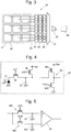
- Fig. 2 shows a partial configuration corresponding to one photosensitive element in the PD detector 10 of the present embodiment.
- the photosensitive-element area 11 has a size of 10 mm ⁇ 10 mm and is divided into 100 (10 ⁇ 10) photosensitive sub-element areas 12 (although Fig. 2 shows only nine of them), with one photodiode placed in each photosensitive sub-element area 12.
- the photodiode in each photosensitive sub-element area 12 is connected through one of the independently provided signal-reading lines 13 to one of the detection circuits 14 placed outside the photosensitive-element area 11.
- Each of the detection circuits 14 is an integrator circuit including a capacitor 102 and amplifier 103, as in the conventional PD detector already illustrated with reference to Fig. 1 .
- Each detection circuit 14 has an analog-to-digital (A/D) converter 15 and digital memory 16 connected in series.
- the numbers of the detection circuits 14, A/D converters 15 and digital memories 16 are the same as that of the photosensitive sub-element areas 12 (i.e. 100), although only nine of each of these elements are shown.
- the signals stored in the 100 digital memories 16 are sequentially read by a multiplexer 17 and sent to a digital computing unit 19 through the output port of a high-speed digital output circuit 18 connected to the multiplexer 17.
- the digital computing unit 19 totals the 100 output signals and provides the total signal as the output signal for one photosensitive element at predetermined intervals of sampling time.
- the S/N ratio of the photodetector in the present embodiment under specific measurement conditions is hereinafter described.
- the accumulation time (which corresponds to the sampling period) is 10 ms.
- the maximum number of photons incident on the photosensitive-element area 11 during the accumulation time is 2 ⁇ 10 9 .
- the maximum value of the voltage in the detection circuit 14 (the voltage value produced upon incidence of the maximum number of photons) is 10 V.
- the electrical noise is 100 ⁇ V.
- the maximum number of electrons generated within each photosensitive sub-element area 12 is 10 7 . Accordingly, the integral capacitance C of each capacitor 102 can be decreased to 0.16 pF.
- K is the number of photosensitive sub-element areas 12 in the photosensitive-element area 11, which is 100 in the present configuration example.
- Parameter m is the number of electrons generated in the photodiode placed in the sub-element area.
- the S/N ratio calculated by equation (8) is 707, which is much higher than the S/N ratio of the conventional PD detector, i.e. 99.5.
- K • m n 2 representing the electrical noise in equation (8) has a value of 10 6 .
- the photodiode is in the form of a package and mounted on a printed circuit board along with the integrator circuit having an analog IC and capacitor, the number of noise electrons increases due to the parasitic capacitance of the package of the photodiode and/or analog IC as well as the parasitic capacitance due to the wiring on the printed circuit. Since these parasitic capacitances are also on the order of pF, it is practically difficult to construct an integration amplifier having a high gain as obtained by the previously described calculation. Accordingly, at least the portion of the integration amplifier in the detection circuit should preferably be integrally formed on the same semiconductor integrated circuit board as the photodiode.
- a device having such a configuration and manufactured by a CMOS process which is capable of micro-wiring is hereinafter described as the second embodiment.
- CMOS devices are operated at a low supply voltage. Therefore, in many cases, it is impossible to handle a high voltage of 10 V within the device, as in the first embodiment. Accordingly, the following description deals with an example in which the upper limit of the voltage that can be handled within the device is 1 V, while the electrical noise is the same as in the previous case, i.e. 100 ⁇ V.
- Fig. 3 is a partial configuration diagram corresponding to one photosensitive element in the PD detector 20 of the second embodiment.
- This detector has a similar configuration to that of the PD detector 10 of the first embodiment.
- the detection circuit in the second embodiment is included in each photosensitive sub-element area 22, as shown in Fig. 4 .
- a correlated double sampling circuit (CDS circuit) 24 is placed between the detection circuit and the A/D converter 25.
- CDS circuit correlated double sampling circuit
- the elements arranged within the photosensitive sub-element area 22 are as follows: a photodiode 31; a transfer transistor 32, provided at the end of a signal-reading line connected to the photodiode 31, for transferring photocharges; a floating diffusion 33, connected to the photodiode 31 via the transfer transistor 32, for temporarily accumulating photocharges and converting those charges into a voltage signal; a reset transistor 34 for removing electric charges accumulated in the floating diffusion 33; and a source follower amplifier 35 formed by two cascade-arranged transistors 351 and 352, for providing, as a voltage signal, the electric charges accumulated in the floating diffusion 33.
- Power sources V DD are connected to the reset transistor 34 and the transistor 351, respectively.
- a constant voltage (bias voltage) V BIAS is connected to the gate of the transistor 352.
- Drive lines (not shown) for supplying control signals ⁇ T and ⁇ R are connected to the gate of the transfer transistor 32 and that of the reset transistor 34, respectively. Based on the control signals supplied through these drive lines, the intensity of the light incident on the photodiode 31 is detected at predetermined intervals of sampling time.
- the S/N ratio in the configuration of the second embodiment is hereinafter calculated under the same conditions as in the first embodiment except that the upper limit of the voltage is 1 V.
- the detection circuit is located within the photosensitive sub-element area 22 as shown in Fig. 4 , a high conversion gain can be achieved by reducing the influence of the parasitic capacitance due to the wiring.
- the accumulation of the photocurrent in the second embodiment is performed within the photosensitive sub-element area 22.
- the photoelectrons generated in the photodiode 31 during the accumulation time (sampling period) are electrically transferred through the reading gate (transfer transistor 32) into the diffusion layer of the floating diffusion (FD) and converted into voltage through the capacitance of the diffusion layer.
- a configuration having a low capacitance of 16 fF can be embodied.
- Equation (9) shows that the lower the integral capacitance C is, the higher the reset noise becomes.
- the reset noise is 509 ⁇ V, which is more than five times as high as the electrical noise.
- a correlated double sampling circuit (CDS circuit) 24 as shown in Fig, 5 is provided.
- the CDS circuit 24 includes two selection transistors 361 and 362, two capacitors 371 and 372, as well as a differential amplifier 38.
- the reset noise can be removed by sampling the voltage at the point in time where the floating diffusion is reset as well as the voltage at the point in time after the photoelectrons are transferred to the floating diffusion, and computing the difference between the two voltages.
- the output signals from the CDS circuits 24 are converted into digital signals by the A/D converters 25. After being stored in the digital memories 26, those signals are sequentially read by the multiplexer 27 and sent to the digital computing unit 29 through the output port of the high-speed digital output circuit 28.
- the digital computing unit 29 totals the output signals from all photosensitive sub-element areas 22 and provides the total signal as the output signal for one photosensitive element.
- Fig. 6 is a graph comparing the S/N ratio of the PD detector 20 of the second embodiment with that of a conventional PD detector. As shown in this graph, by using the PD detector 20 of the second embodiment, it is possible to increase the S/N ratio to a level which is higher than that of the conventional PD detector by more than one order of magnitude and closer to the level of an ideal detector (i.e. a PD detector in which no electrical noise occurs).
- Fig. 7 shows the configuration of a PD detector 40 of the third embodiment.
- this PD detector 40 seven photosensitive-element areas 41 are arrayed in the vertical direction in the figure, with each photosensitive-element area 41 divided into 1000 photosensitive sub-element areas 42 in the horizontal direction (although only seven of them are shown in the figure).
- the photosensitive-element area 41 has a size of 2.5 ⁇ m ⁇ 2.5 mm, while each photosensitive sub-element area 42 has a size of 2.5 ⁇ m ⁇ 2.5 ⁇ m.
- Each photosensitive-element area 41 is provided with one signal-reading line 43, which is shared by the photosensitive sub-element areas 42 included in the photosensitive-element area 41 concerned.
- a CDS circuit 44, A/D converter 45 and digital memory 46 corresponding to each photosensitive element are provided at the end of the signal-reading line 43, along with a multiplexer 47 for sequentially reading the signals stored in the digital memories 46, as well as a high-speed digital output circuit 48 and digital computing unit 49.
- the plurality of detection circuits (capacitors) (photosensitive sub-element areas 42) in the photosensitive-element areas 41 are organized into one or more groups, while the signal processing section has one A/D converter 45 and one digital memory 46 (signal storage section) for each group.
- the digital computing unit 49 performs appropriate operations according to the purpose of the analysis, such as averaging the signals detected by the detection circuits corresponding to the photosensitive-element areas 41 or calculating a difference between those signals.
- the digital computing unit 49 may also be configured to calculate a difference in the signal continuously produced from the same photosensitive element over a period of time based on analysis conditions specified by an analysis operator on a separate control device.
- a specific configuration is as follows: An output signal corresponding to only the background light is initially acquired in the first accumulation period. Subsequently, in each accumulation period, an output signal corresponding to the sum of the background light and measurement light is acquired, and the former output signal is subtracted from the latter. The result of this calculation is sent to an external system as the output signal corresponding to the measurement light.
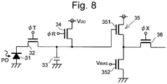
- Fig. 8 is a circuit configuration diagram in the photosensitive sub-element area 42. As with the circuit described in the second embodiment using Fig. 3 , this circuit includes a photodiode 31, transfer transistor 32 for transferring photocharges, floating diffusion 33, reset transistor 34, as well as a source follower amplifier 35 formed by two transistors 351 and 352. In addition, a selection gate 36 is placed behind the source follower amplifier 35.
- the predetermined interval of sampling time at which the digital computing unit 49 provides an output signal obtained by totaling the signals from the photosensitive elements is divided (i.e. frequency-divided) into sub-periods (e.g. 1000 sub-periods), while the selection gates 36 in the 1000 photosensitive sub-element areas 42 are sequentially supplied with control signal ⁇ X (a signal which indicates the sub-period) through their respective gate terminals.
- control signal ⁇ X a signal which indicates the sub-period
- the photocurrents produced by the 1000 photodiodes 31 belonging to the same photosensitive-element area 41 are sequentially read from one photosensitive sub-element area 42 in each sub-period, and temporarily stored in the digital memories 46.
- the stored signals are totaled by the digital computing unit 49 at the predetermined intervals of sampling time and provided as the output signal.
- the term representing the electronical noise in the third embodiment has a larger value than in the second embodiment, this value can be appropriately decreased by increasing the number of divisions of the photosensitive-element area 41.
- each photosensitive element is provided with one signal-reading line 43 and other related elements. It is also possible to adopt a different configuration. For example, the number of divisions of the sampling period can be decreased to one half of the number of photosensitive sub-element areas by dividing the photosensitive sub-element areas 42 arranged within each photosensitive-element area 41 into two groups and providing each group with one signal-reading line 43 and other related elements.
- the configurations described in the previous embodiments not only increase the S/N ratio by decreasing the magnitude of the electrical noise but also improve the yield rate of the chip-manufacturing process.
- the circuit wiring is formed on a semiconductor substrate by mask-pattern projection. In this process, foreign matters (e.g. particles) may adhere to the wafer surface. If this occurs, the desired circuit wiring cannot be formed, and a spot region in which the dark current or leak current specifically increases is formed. If such a spot region is formed in one of the photosensitive elements in a conventional PD array detector, the entire array detector will be treated as a defective product due to that single photosensitive element, since each photosensitive element has only one combination of the PD and the detection circuit inside.
- the photosensitive-element area is divided into a plurality of photosensitive sub-element areas, with each photosensitive sub-element area having a PD and detection circuit arranged for it. Even if a spot region has occurred in one of the L divisions of the photosensitive-element area, a correct output signal can still be obtained by converting the L -1 available detection signals into L signals or by performing a computing process for estimating the signal value at the spot region from the detection signals obtained at the photosensitive sub-element areas adjacent to the spot region. Accordingly, the array detector will not be treated as a defective product, so that the yield rate will be improved.
- the digital computing unit 49 can be configured to disregard a specific photosensitive sub-element area and perform a computing process using only the output signals from the other photosensitive sub-element areas.
- any of the previous embodiments is a mere example and can be appropriately changed without departing from the spirit of the present invention.
- the A/D converters are provided so as to read signals at high speeds. However, those A/D converters are unnecessary in the case where the voltage signals are processed in analog form.
- the number of divisions of the photosensitive-element area in each embodiment is also a mere example and may be appropriately changed.
- the configuration in any of the embodiments is applicable in any type of array detector having a plurality of photosensitive-element areas arranged in a one-dimensional or two-dimensional form.
- the computing processes performed by the digital computing unit described in the third embodiment are also mere examples; for example, the digital computing unit may be configured to perform an appropriate computing process according to the content of the analysis using an analyzing device which includes a PD detector according to one of the previous embodiments.
- the equations which do not take into account the influence of the shot noise resulting from the dark current (which is hereinafter called the "dark-current shot noise") were used to calculate the S/N ratio.
- the dark-current shot noise A case in which the dark-current shot noise is considered is hereinafter described.
Landscapes
- Engineering & Computer Science (AREA)
- Multimedia (AREA)
- Signal Processing (AREA)
- Physics & Mathematics (AREA)
- Spectroscopy & Molecular Physics (AREA)
- General Physics & Mathematics (AREA)
- Power Engineering (AREA)
- Photometry And Measurement Of Optical Pulse Characteristics (AREA)
- Solid State Image Pick-Up Elements (AREA)
- Transforming Light Signals Into Electric Signals (AREA)
Applications Claiming Priority (2)
| Application Number | Priority Date | Filing Date | Title |
|---|---|---|---|
| JP2014235966 | 2014-11-20 | ||
| PCT/JP2015/069693 WO2016080016A1 (fr) | 2014-11-20 | 2015-07-08 | Détecteur optique |
Publications (2)
| Publication Number | Publication Date |
|---|---|
| EP3220628A1 true EP3220628A1 (fr) | 2017-09-20 |
| EP3220628A4 EP3220628A4 (fr) | 2017-10-18 |
Family
ID=56013581
Family Applications (1)
| Application Number | Title | Priority Date | Filing Date |
|---|---|---|---|
| EP15861720.9A Withdrawn EP3220628A4 (fr) | 2014-11-20 | 2015-07-08 | Détecteur optique |
Country Status (5)
| Country | Link |
|---|---|
| US (1) | US20170336254A1 (fr) |
| EP (1) | EP3220628A4 (fr) |
| JP (1) | JPWO2016080016A1 (fr) |
| CN (1) | CN107005664A (fr) |
| WO (1) | WO2016080016A1 (fr) |
Cited By (1)
| Publication number | Priority date | Publication date | Assignee | Title |
|---|---|---|---|---|
| US11604146B2 (en) | 2017-09-19 | 2023-03-14 | Beckman Coulter, Inc. | Analog light measuring and photon counting with a luminometer system for assay reactions in chemiluminescence measurements |
Families Citing this family (2)
| Publication number | Priority date | Publication date | Assignee | Title |
|---|---|---|---|---|
| WO2019102636A1 (fr) | 2017-11-24 | 2019-05-31 | 浜松ホトニクス株式会社 | Dispositif de comptage de photons et procédé de comptage de photons |
| CN110278396B (zh) * | 2018-03-16 | 2024-07-12 | 松下知识产权经营株式会社 | 摄像装置 |
Family Cites Families (18)
| Publication number | Priority date | Publication date | Assignee | Title |
|---|---|---|---|---|
| JPH07306133A (ja) * | 1994-03-14 | 1995-11-21 | Hitachi Electron Eng Co Ltd | 微粒子検出器 |
| JP4007716B2 (ja) * | 1999-04-20 | 2007-11-14 | オリンパス株式会社 | 撮像装置 |
| US6437325B1 (en) * | 1999-05-18 | 2002-08-20 | Advanced Research And Technology Institute, Inc. | System and method for calibrating time-of-flight mass spectra |
| JP3774597B2 (ja) * | 1999-09-13 | 2006-05-17 | キヤノン株式会社 | 撮像装置 |
| US6914227B2 (en) * | 2001-06-25 | 2005-07-05 | Canon Kabushiki Kaisha | Image sensing apparatus capable of outputting image by converting resolution by adding and reading out a plurality of pixels, its control method, and image sensing system |
| JP3904111B2 (ja) * | 2002-06-04 | 2007-04-11 | ソニー株式会社 | 固体撮像装置及びその信号処理方法 |
| JP4689620B2 (ja) * | 2004-11-02 | 2011-05-25 | パナソニック株式会社 | イメージセンサ |
| WO2008106587A1 (fr) * | 2007-02-28 | 2008-09-04 | Stoneridge, Inc. | Dispositif de filtration destiné à être utilisé avec un système de récupération de vapeur de carburant |
| JP4931238B2 (ja) * | 2007-08-14 | 2012-05-16 | キヤノン株式会社 | 撮像装置及びその駆動方法 |
| WO2009031302A1 (fr) * | 2007-09-05 | 2009-03-12 | Tohoku University | Élément d'imagerie à semi-conducteurs et son procédé d'excitation |
| JP4500862B2 (ja) * | 2008-04-11 | 2010-07-14 | キヤノン株式会社 | 固体撮像装置の駆動方法 |
| JP4661912B2 (ja) * | 2008-07-18 | 2011-03-30 | ソニー株式会社 | 固体撮像素子およびカメラシステム |
| JP2010078338A (ja) * | 2008-09-24 | 2010-04-08 | Toshiba Corp | X線検出器 |
| JP2010212536A (ja) * | 2009-03-12 | 2010-09-24 | Sony Corp | 固体撮像装置の製造方法 |
| JP5511541B2 (ja) * | 2010-06-24 | 2014-06-04 | キヤノン株式会社 | 固体撮像装置及び固体撮像装置の駆動方法 |
| JP5991045B2 (ja) * | 2012-06-28 | 2016-09-14 | 住友電気工業株式会社 | 半導体装置 |
| JP2014049727A (ja) * | 2012-09-04 | 2014-03-17 | Canon Inc | 固体撮像装置 |
| JP6164867B2 (ja) * | 2013-02-21 | 2017-07-19 | キヤノン株式会社 | 固体撮像装置、その制御方法、および制御プログラム |
-
2015
- 2015-07-08 EP EP15861720.9A patent/EP3220628A4/fr not_active Withdrawn
- 2015-07-08 CN CN201580063631.0A patent/CN107005664A/zh not_active Withdrawn
- 2015-07-08 WO PCT/JP2015/069693 patent/WO2016080016A1/fr not_active Ceased
- 2015-07-08 US US15/528,188 patent/US20170336254A1/en not_active Abandoned
- 2015-07-08 JP JP2016560079A patent/JPWO2016080016A1/ja active Pending
Cited By (2)
| Publication number | Priority date | Publication date | Assignee | Title |
|---|---|---|---|---|
| US11604146B2 (en) | 2017-09-19 | 2023-03-14 | Beckman Coulter, Inc. | Analog light measuring and photon counting with a luminometer system for assay reactions in chemiluminescence measurements |
| US11754504B2 (en) | 2017-09-19 | 2023-09-12 | Beckman Coulter, Inc. | System for analog light measuring and photon counting in chemiluminescence measurements |
Also Published As
| Publication number | Publication date |
|---|---|
| EP3220628A4 (fr) | 2017-10-18 |
| US20170336254A1 (en) | 2017-11-23 |
| JPWO2016080016A1 (ja) | 2017-07-13 |
| WO2016080016A1 (fr) | 2016-05-26 |
| CN107005664A (zh) | 2017-08-01 |
Similar Documents
| Publication | Publication Date | Title |
|---|---|---|
| US9121955B2 (en) | Single photon counting detector system having improved counter architecture | |
| CN108139268B (zh) | 光学脉冲检测装置、光学脉冲检测方法、辐射计数装置和生物测试装置 | |
| US10063784B2 (en) | Imaging apparatus, an electronic device, and imaging method to uniformize distribution of incident light, and a photostimulated luminescence detection scanner | |
| US11828653B2 (en) | Spectrometric device and spectrometric method | |
| Köklü et al. | Characterization of standard CMOS compatible photodiodes and pixels for lab-on-chip devices | |
| US20100025588A1 (en) | Determining diffusion length of minority carriers using luminescence | |
| CN104237926A (zh) | 光探测器和计算断层摄影装置 | |
| US20130214134A1 (en) | Photon detector | |
| Bonanno et al. | Characterization measurements methodology and instrumental set-up optimization for new SiPM detectors—Part II: Optical tests | |
| Finger et al. | Interpixel capacitance in large format CMOS hybrid arrays | |
| EP3220628A1 (fr) | Détecteur optique | |
| Greulich et al. | Contactless measurement of current-voltage characteristics for silicon solar cells | |
| Greffe et al. | Characterization of low light performance of a complementary metal-oxide semiconductor sensor for ultraviolet astronomical applications | |
| Apergis et al. | High-precision photometry with a scientific CMOS camera: I lab testing of the Marana camera | |
| CN118089942A (zh) | 一种基于半导体光电二极管的计算型光谱仪光谱重构的优化方法 | |
| US11665441B2 (en) | Detector, methods for operating a detector and detector pixel circuit | |
| US10129494B2 (en) | Imaging device, and solid-state image sensor | |
| Treis et al. | Advancements in DEPMOSFET device developments for XEUS | |
| WO2025030313A1 (fr) | Détecteurs de rayonnement à transistors à oxyde d'indium-zinc | |
| US20250258039A1 (en) | Spectroscopy device, raman spectroscopic measurement device, and spectroscopy method | |
| US20250189453A1 (en) | Spectroscopic device, raman spectroscopic measurement device, and spectroscopic method | |
| Poklonskaya et al. | Line sensor for fast, time-resolved spectroscopy measurements | |
| Labusov et al. | Measuring the quantum efficiency of multielement photodetectors in the spectral range between 180 and 800 nm | |
| Gasparian et al. | Advances in InGaAs multielement linear arrays | |
| Pike et al. | Comparison of proton damage effects in standard and enhanced depletion CMOS image sensors |
Legal Events
| Date | Code | Title | Description |
|---|---|---|---|
| PUAI | Public reference made under article 153(3) epc to a published international application that has entered the european phase |
Free format text: ORIGINAL CODE: 0009012 |
|
| 17P | Request for examination filed |
Effective date: 20170616 |
|
| AK | Designated contracting states |
Kind code of ref document: A1 Designated state(s): AL AT BE BG CH CY CZ DE DK EE ES FI FR GB GR HR HU IE IS IT LI LT LU LV MC MK MT NL NO PL PT RO RS SE SI SK SM TR |
|
| AX | Request for extension of the european patent |
Extension state: BA ME |
|
| A4 | Supplementary search report drawn up and despatched |
Effective date: 20170918 |
|
| RIC1 | Information provided on ipc code assigned before grant |
Ipc: H04N 5/378 20110101ALI20170912BHEP Ipc: H04N 5/3745 20110101ALI20170912BHEP Ipc: H04N 5/357 20110101ALI20170912BHEP Ipc: G01J 1/42 20060101AFI20170912BHEP Ipc: G01J 1/46 20060101ALI20170912BHEP |
|
| DAV | Request for validation of the european patent (deleted) | ||
| DAX | Request for extension of the european patent (deleted) | ||
| 17Q | First examination report despatched |
Effective date: 20180705 |
|
| STAA | Information on the status of an ep patent application or granted ep patent |
Free format text: STATUS: THE APPLICATION IS DEEMED TO BE WITHDRAWN |
|
| 18D | Application deemed to be withdrawn |
Effective date: 20190116 |